US12237765B2 - DC-DC transformer with inductor for the facilitation of adiabatic inter-capacitor charge transport - Google Patents
DC-DC transformer with inductor for the facilitation of adiabatic inter-capacitor charge transport Download PDFInfo
- Publication number
- US12237765B2 US12237765B2 US18/194,861 US202318194861A US12237765B2 US 12237765 B2 US12237765 B2 US 12237765B2 US 202318194861 A US202318194861 A US 202318194861A US 12237765 B2 US12237765 B2 US 12237765B2
- Authority
- US
- United States
- Prior art keywords
- terminal
- voltage
- charge pump
- regulator
- switches
- Prior art date
- Legal status (The legal status is an assumption and is not a legal conclusion. Google has not performed a legal analysis and makes no representation as to the accuracy of the status listed.)
- Active
Links
Images


Classifications
-
- H—ELECTRICITY
- H02—GENERATION; CONVERSION OR DISTRIBUTION OF ELECTRIC POWER
- H02M—APPARATUS FOR CONVERSION BETWEEN AC AND AC, BETWEEN AC AND DC, OR BETWEEN DC AND DC, AND FOR USE WITH MAINS OR SIMILAR POWER SUPPLY SYSTEMS; CONVERSION OF DC OR AC INPUT POWER INTO SURGE OUTPUT POWER; CONTROL OR REGULATION THEREOF
- H02M1/00—Details of apparatus for conversion
- H02M1/0095—Hybrid converter topologies, e.g. NPC mixed with flying capacitor, thyristor converter mixed with MMC or charge pump mixed with buck
-
- H—ELECTRICITY
- H02—GENERATION; CONVERSION OR DISTRIBUTION OF ELECTRIC POWER
- H02M—APPARATUS FOR CONVERSION BETWEEN AC AND AC, BETWEEN AC AND DC, OR BETWEEN DC AND DC, AND FOR USE WITH MAINS OR SIMILAR POWER SUPPLY SYSTEMS; CONVERSION OF DC OR AC INPUT POWER INTO SURGE OUTPUT POWER; CONTROL OR REGULATION THEREOF
- H02M1/00—Details of apparatus for conversion
- H02M1/0067—Converter structures employing plural converter units, other than for parallel operation of the units on a single load
-
- H—ELECTRICITY
- H02—GENERATION; CONVERSION OR DISTRIBUTION OF ELECTRIC POWER
- H02M—APPARATUS FOR CONVERSION BETWEEN AC AND AC, BETWEEN AC AND DC, OR BETWEEN DC AND DC, AND FOR USE WITH MAINS OR SIMILAR POWER SUPPLY SYSTEMS; CONVERSION OF DC OR AC INPUT POWER INTO SURGE OUTPUT POWER; CONTROL OR REGULATION THEREOF
- H02M3/00—Conversion of DC power input into DC power output
- H02M3/02—Conversion of DC power input into DC power output without intermediate conversion into AC
- H02M3/04—Conversion of DC power input into DC power output without intermediate conversion into AC by static converters
- H02M3/06—Conversion of DC power input into DC power output without intermediate conversion into AC by static converters using resistors or capacitors, e.g. potential divider
- H02M3/07—Conversion of DC power input into DC power output without intermediate conversion into AC by static converters using resistors or capacitors, e.g. potential divider using capacitors charged and discharged alternately by semiconductor devices with control electrode, e.g. charge pumps
- H02M3/073—Charge pumps of the Schenkel-type
-
- H—ELECTRICITY
- H02—GENERATION; CONVERSION OR DISTRIBUTION OF ELECTRIC POWER
- H02M—APPARATUS FOR CONVERSION BETWEEN AC AND AC, BETWEEN AC AND DC, OR BETWEEN DC AND DC, AND FOR USE WITH MAINS OR SIMILAR POWER SUPPLY SYSTEMS; CONVERSION OF DC OR AC INPUT POWER INTO SURGE OUTPUT POWER; CONTROL OR REGULATION THEREOF
- H02M3/00—Conversion of DC power input into DC power output
- H02M3/02—Conversion of DC power input into DC power output without intermediate conversion into AC
- H02M3/04—Conversion of DC power input into DC power output without intermediate conversion into AC by static converters
- H02M3/10—Conversion of DC power input into DC power output without intermediate conversion into AC by static converters using discharge tubes with control electrode or semiconductor devices with control electrode
- H02M3/145—Conversion of DC power input into DC power output without intermediate conversion into AC by static converters using discharge tubes with control electrode or semiconductor devices with control electrode using devices of a triode or transistor type requiring continuous application of a control signal
- H02M3/155—Conversion of DC power input into DC power output without intermediate conversion into AC by static converters using discharge tubes with control electrode or semiconductor devices with control electrode using devices of a triode or transistor type requiring continuous application of a control signal using semiconductor devices only
- H02M3/156—Conversion of DC power input into DC power output without intermediate conversion into AC by static converters using discharge tubes with control electrode or semiconductor devices with control electrode using devices of a triode or transistor type requiring continuous application of a control signal using semiconductor devices only with automatic control of output voltage or current, e.g. switching regulators
- H02M3/158—Conversion of DC power input into DC power output without intermediate conversion into AC by static converters using discharge tubes with control electrode or semiconductor devices with control electrode using devices of a triode or transistor type requiring continuous application of a control signal using semiconductor devices only with automatic control of output voltage or current, e.g. switching regulators including plural semiconductor devices as final control devices for a single load
- H02M3/1584—Conversion of DC power input into DC power output without intermediate conversion into AC by static converters using discharge tubes with control electrode or semiconductor devices with control electrode using devices of a triode or transistor type requiring continuous application of a control signal using semiconductor devices only with automatic control of output voltage or current, e.g. switching regulators including plural semiconductor devices as final control devices for a single load with a plurality of power processing stages connected in parallel
-
- Y—GENERAL TAGGING OF NEW TECHNOLOGICAL DEVELOPMENTS; GENERAL TAGGING OF CROSS-SECTIONAL TECHNOLOGIES SPANNING OVER SEVERAL SECTIONS OF THE IPC; TECHNICAL SUBJECTS COVERED BY FORMER USPC CROSS-REFERENCE ART COLLECTIONS [XRACs] AND DIGESTS
- Y02—TECHNOLOGIES OR APPLICATIONS FOR MITIGATION OR ADAPTATION AGAINST CLIMATE CHANGE
- Y02B—CLIMATE CHANGE MITIGATION TECHNOLOGIES RELATED TO BUILDINGS, e.g. HOUSING, HOUSE APPLIANCES OR RELATED END-USER APPLICATIONS
- Y02B70/00—Technologies for an efficient end-user side electric power management and consumption
- Y02B70/10—Technologies improving the efficiency by using switched-mode power supplies [SMPS], i.e. efficient power electronics conversion e.g. power factor correction or reduction of losses in power supplies or efficient standby modes
Definitions
- This disclosure relates to power conversion, and in particular, to DC power conversion.
- a known power converter is obtained by placing a regulator in series with a charge pump.
- An example of such a regulator operates by switching an inductor into one state and into a second state according to some switch duty cycle.
- the inductor in this regulator performs two functions. One is to control the output voltage of the converter. The other is to promote adiabatic charge transfer among the capacitors within the charge pump.
- the invention is based on the recognition that the regulator's dual function of regulation and promoting adiabatic charge transfer can be carried out by different components.
- the invention includes reducing the functionality of a component that has always been used to carry out two functions and relocating it so that it can no longer carry out one of those functions.
- a new circuit component is added to carry out the function that used to be carried out by the existing component. The invention thus achieves a more complex circuit with an additional component that was not needed in the prior art.
- the invention also reduces the die area required for the circuit by increasing the number of components that have to be placed on the die.
- the invention described herein also fills in certain holes in the performance of the overall power converter and makes it possible to carry out more of the voltage transformation within the charge pump, where it can be done most efficiently.
- one or more arrangements of a power converter are made up of a combination of an interconnection of sections, including at least a “voltage transformer,” a “magnetic filter,” and a “current regulator,” wherein these denotations have no further implicit connotations.
- the power converter has terminals that include a first pair of terminals and a second pair of terminals, also referred to as the “controller” pair of terminals.
- an operating power converter controls a voltage measured between the controlled pair of terminals.
- the power converter accepts power at the first pair of terminals from a power source (e.g., an unregulated voltage source), referred to as the “powered” pair of terminals, and provides power at a controlled voltage at the second pair of terminals (e.g., to a substantially resistive load), referred to as the “load” pair of terminals.
- a power source e.g., an unregulated voltage source
- the second pair of terminals e.g., to a substantially resistive load
- the voltage transformer which is not to be confused with a conventional magnetic core alternating current “transformer,” has a least three terminals and comprises a switched arrangement of capacitors.
- sequential operation of switches in the voltage transformer causes a voltage transformation, generally by a rational multiple, between a first pair of terminals of the voltage transformer and a second pair of terminals of the voltage transformer.
- one pair of terminals is associated with a higher voltage than the other pair.
- These pairs of terminals are hereinafter referred to as the “high voltage” pair of terminals and the “low voltage” pair of terminals, respectively.
- the sequential operation of the switches causes charge to transfer between capacitors of the voltage transformer.
- the rate of charge transfer is constrained by a current through at least one of the terminals of the voltage transformer. This terminal will be referred to as a “charge transfer rate constraint” terminal.
- the voltage transformer When the rate of charge transfer between capacitors in at least one capacitor of the voltage transformer is constrained for at least some of the time, for example, by the current at the charge transfer rate constraint terminals, the voltage transformer is deemed to be “adiabatic.” If at least some but not necessarily all of the charge transfers are controlled, the voltage transformer is termed “partially adiabatic.” Otherwise the voltage transformer is “fully adiabatic.”
- the magnetic filter comprises two terminals coupled in a circuit path without any switching activity.
- the magnetic filter opposes changes in the current flowing through at least one of the terminals, hereinafter referred to as the “filtered terminal(s)” of the magnetic filter, and generally maintains a substantially constant current through the filtered terminal(s) during steady state operation of the power converter.
- the circuit path joining the terminals includes a passive inductor. In any case, because the path between the two terminals does not require a switch, there is no switch on the path that must be sized or selected to accommodate the maximum voltage or current that may be present on the path during operation.
- the current regulator has at least two terminals and comprises a switched arrangement of at least one inductor.
- controlled sequential operation of one or more switches of the current regulator controls current flow through a least one of the terminals, hereinafter referred to as a “controlled terminal,” of the current regulator.
- the current regulator may regulate current flow, the regulation of current flow may be based on the output voltage (e.g., a time average voltage), which may be measured between a pair of terminals of the current regulator, or between other terminals within or at the interface of the power converter.
- a common feature of a number of embodiments is that the arrangement of the voltage transformer, magnetic filter, and current regulator of the power converter is that a filtered terminal of the magnetic filter is directly coupled (i.e., without intervening switches) to a first terminal of the voltage transformer, with this first terminal being a charge transfer control terminal.
- the magnetic filter is so coupled to a low voltage pair of terminals, recognizing that generally, the magnitude of current flow is higher at the low voltage terminals that at the high voltage terminals of the voltage transformer.
- the controlled terminal of the current regulator is directly coupled (i.e., without intervening switches) to a second terminal (different than the first terminal) of the voltage transformer.
- the second terminal may be, but is not necessarily, a charge transfer rate control terminal of the voltage transformer.
- the current regulator is coupled to multiple terminals of the voltage transformer, or to multiple separate voltage transformer sections of the power converter. In other examples, multiple current regulators, or current regulators having multiple separate controlled terminals, are coupled to multiple terminals of the voltage transformer or to multiple separate voltage transformers.
- the current regulator is controlled to achieve a controlled voltage at the controlled terminals of the power converter.
- a number of configurations of the voltage transformer, magnetic filter, and current regulator can be grouped into (possibly overlapping) classes referred to as “series,” “sigma,” and “pseudo series,” without connoting any particular attributes by these names.
- the series class of configurations includes configurations in which the current regulator, the voltage transformer, and the magnetic filter are connected in series between the first pair and the second pair of terminals of the power converter.
- the magnetic filter is coupled to a controlled/load terminals of the power converter, and the current regulator is coupled to a powered terminal of the regulator.
- the magnetic filter is coupled to a powered terminal of the power converter and the current regulator is coupled to a controlled terminal of the power converter.
- the sigma class and the pseudo series class of configurations include configurations in which one controlled terminal of the current regulator is coupled to a controlled terminal of the power converter.
- the voltage transformer is also coupled to the same (or potentially a different) controlled terminal of the power converter via the magnetic filter such that the magnetic filter provides a path from a charge transfer rate control terminal of the voltage transformer to the controlled terminal.
- another terminal of the current regulator is coupled to the voltage transformer, such that in operation, control of the current regulator affects a voltage on the first pair or the second pair of terminals of the voltage transformer.
- a terminal of the first pair of terminals of the voltage transformer is coupled via the magnetic filter to a controlled terminal of the power converter to which a controlled terminal of the current regulator is also coupled, then another terminal of the current regulator is coupled to a terminal of the second pair of terminals of the voltage transformer.
- the sigma class of configurations includes configurations in which there exists a path from a terminal of the first pair of terminals of the power converter to a terminal of the second pair of terminals of the power converter that passes through the current regulator without passing through the voltage transformer.
- the pseudo series class of configurations includes configurations in which the voltage transformer is coupled to a controlled terminal of the power converter through a first path that passes via the magnetic filter but not the current regulator, as well as via a second path that that passes via the current regulator but not the magnetic filter.
- An advantage of at least some configurations of the sigma and the pseudo parallel classes is that some of the power flow through the power converter passes through the magnetic filter but not the current regulator. Because the magnetic filter does not introduce a switch on power flow path though the magnetic filter, power losses (e.g., resistive and capacitive losses in a switch) are reduced and overall efficiency of the power converter is improved.
- An advantage of at least some configurations of any of the classes are that the number or range of combinations of terminal voltages supported by the power converted can be increases as compared to other configurations that are affected by limitations on voltage differences between pair of its terminals of the current regulator that differ by less than a threshold voltage.
- Another advantage of at least some configurations is that voltage or current handling requirements of switches of the voltage transformed and/or the current regulator can be reduced as compared to other configurations. These reduced requirements can result in physically smaller semiconductor devices, which can reduce the size of an integrated circuit implementation of some or all of the power converter.
- the invention features a power converter that transforms a first voltage at a first power-converter terminal into a second voltage at a second power-converter terminal.
- the power converter includes a switching network in which switches that operate at a common frequency and duty cycle interconnect certain circuit elements. These circuit elements include a magnetic filter and capacitors.
- the magnetic filter includes first and second magnetic-filter terminals, with the second magnetic-filter terminal being maintained at the second voltage. When connected to the capacitors by a switch from the switching network, the magnetic filter imposes a constraint upon inter-capacitor charge transfer between the capacitors.
- states include at least first, second, and third states.
- the first magnetic-filter terminal couples to the capacitor network.
- the second state which occurs between the first and third states, the switches ground the first magnetic-filter terminal is grounded
- Embodiments include those in which the the capacitors and the switching network cooperate to define a single-phase charge pump and those in which they cooperate to define a multi-phase charge pump.
- the first magnetic-filter terminal couples to a node, a cathode of a first capacitor connects to the node, and an anode of a second capacitor connects to the node.
- cathodes of the first and second capacitors connect to each other and the first magnetic-filter terminal connects to an anode of one of the first and second capacitors.
- the switching network executes a cycle that begins with a transition out of the fourth state and ends with a transition into the fourth state.
- the cycle consists of four transitions between states and those in which the cycle consists of only three transitions between states.
- the switching network comprises a stabilizing switch that connects a stabilizing capacitor to the first magnetic-filter terminal and disconnects the stabilizing capacitor from the first magnetic-filter terminal.
- a stabilizing switch that connects a stabilizing capacitor to the first magnetic-filter terminal and disconnects the stabilizing capacitor from the first magnetic-filter terminal.
- the second magnetic-filter terminal connects to capacitor.
- the switching network comprises a first switch.
- This first switch connects the first magnetic-filter terminal to the capacitor network and disconnects the first magnetic-filter terminal from the capacitor network.
- embodiments that also include a second switch.
- This second switch connects the first magnetic-filter terminal to ground when the first switch has disconnected the first magnetic-filter terminal from the capacitor network. The the second switch is open otherwise.
- the switching network comprises a first switch.
- the first switch transitions between first and second states.
- the first state connects the first magnetic-filter terminal to ground.
- the second state disconnects the first magnetic-filter terminal from ground.
- the magnetic filter is a constituent of an LC circuit connected to the capacitor network.
- the capacitor network and the switching network cooperate to define a two-phase charge pump.
- Some embodiments include a controller for controlling operation of the regulator based on an output of the power converter. Others include a clock configured to provide a clock signal to either the regulator or the charge pump.
- control system configured to control operation of the power converter based on a measured output of the power converter.
- controllers to control the regulator
- controllers to control the charge pump
- clock signal input that can receive a clock signal
- the controller has digital inputs
- the controller has analog inputs
- the invention features an apparatus that includes switches that interconnect capacitors of a charge pump that connects to a first terminal of a power converter that comprises the charge pump and a regulator.
- a first power path connects the power converter to a first terminal of a magnetic filter and a second power path connects the power converter to a second terminal of the magnetic filter and to a second terminal of the power converter.
- the first power path couples the charge pump to the magnetic filter and the magnetic filter imposes a constraint in inter-capacitor charge transport within the charge pump and wherein a third power path connects the charge pump to the regulator.
- the first power path couples the regulator to the magnetic filter and a third power path connects the charge pump to the regulator.
- Embodiments include those in which the charge pump and the regulator share a common ground and those in which the charge pump has a fixed reference potential and the regulator has a floating reference potential or vice versa.
- charge pumps and regulators can be used.
- charge pumps and regulators can be used.
- those that have a multi-phase charge pump those that have a single-phase charge pump, those that have a multi-stage charge pump, those have a two-phase charge pump, those that have a resonant power converter, those that have a switch mode power converter, those that have a buck converter, those that have a bidirectional regulator, and those that a multi-phase regulator.
- the charge pump comprises capacitors interconnected by sets of switches. During operation, switches in the first set are opposite in state to switches in the second set.
- the charge pump is a reconfigurable charge pump.
- the regulator is configured to transition from providing a first voltage to providing a second voltage during reconfiguration of the charge pump.
- the invention features an apparatus for power transformation.
- Such an apparatus includes a power converter having a charge pump, a first regulator that regulates the power provided by the power converter, and a magnetic filter connected to a terminal of the charge pump.
- the particular terminal to which the magnetic filter is connected is selected to facilitate causing a constraint in inter-capacitor charge transport within the charge pump.
- the invention features a power converter that has switches that cause it to carry out cycles of operation.
- Each cycle of operation comprises connecting a first capacitor network to a first terminal of a magnetic filter, disconnecting the first capacitor network from said first terminal, connecting a second capacitor network to the first terminal, and disconnecting the second capacitor network from said first terminal to end said cycle, wherein disconnecting the first terminal comprises grounding the first terminal.
- connecting the first capacitor network comprises connecting a cathode of a first capacitor to an anode of a second capacitor, connecting the cathode to the first terminal, and connecting the anode to the first terminal.
- the invention features a non-transitory computer-readable medium that stores a data structure that is to be operated upon by a program executable on a computer system, wherein, when operated upon by such a program, the data structure causes at least a portion of a process for fabricating an integrated circuit that includes circuitry described by the data structure, wherein the circuitry described by the data structure includes a switching network that has been configured to be used with a power converter that comprises the components described above.
- FIG. 1 shows one embodiment of a power converter
- FIG. 2 shows a switched-capacitor charge pump for use with a power converter such as that shown in FIG. 1 ;
- FIG. 3 A shows terminals that connect to the various capacitor networks that will be formed and unformed as the charge pump of FIG. 2 transitions through its various states;
- FIG. 3 B shows a first capacitor network corresponding to a first configuration of switches for the charge pump of FIG. 2 ;
- FIG. 3 C shows a second capacitor network corresponding to a second configuration of switches for the charge pump of FIG. 2 ;
- FIG. 4 shows a block diagram of the 4-terminal charge pump of FIG. 2 ;
- FIG. 6 A shows the components of a typical regulator that can be used in a power converter such as that shown in FIG. 1 ;
- FIG. 8 shows an embodiment in which a diode is used to conduct current in a magnetic filter that has no place to go during the dead time of the charge pump
- FIG. 9 shows the power converter of FIG. 1 but with parallel charge pumps and parallel magnetic filters.
- FIG. 14 A shows a circuit that implements the bifurcated power path of FIG. 13 , with the input voltage split so that the voltage presented to the regulator is twice that presented to the charge pump;
- FIG. 15 A shows another embodiment having a bifurcated power path through a power converter
- FIG. 15 B shows a circuit that implements the bifurcated power path of FIG. 15 A ;
- FIG. 16 A shows an isolated charge pump that is suitable for use with the architecture shown in FIG. 15 A ;
- FIG. 16 B shows a single-phase implementation of the isolated charge pump shown in FIG. 16 A ;
- FIG. 16 C shows a two-phase implementation of the isolated charge pump shown in FIG. 16 A ;
- FIGS. 17 A- 17 D show variants of the architecture shown in FIG. 15 A ;
- FIGS. 18 A- 18 C show circuit topologies having bifurcated power paths with grounded charge pumps.
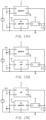
- FIGS. 19 A- 19 C show circuit topologies similar to those in FIGS. 18 A- 18 C except with grounded regulators instead of charge pumps.
- FIG. 20 shows a power converter that shows features common to the embodiments of FIGS. 1 , 12 , 13 , and 15 A ;
- FIG. 21 A shows a regulated charge pump
- FIGS. 21 B- 21 C show the switch configurations and network states for the regulated charge pump of FIG. 21 A ;
- FIG. 22 A shows a regulated charge pump of FIG. 21 A with a switch having been eliminated
- FIG. 22 B shows the switch configurations for the regulated charge pump of FIG. 22 A ;
- FIG. 23 A shows the regulated charge pump of FIG. 22 A with a stabilizing capacitor
- FIGS. 23 B- 23 C show the switch configurations and network states for the regulated charge pump of FIG. 23 A ;
- FIG. 24 A shows a regulated charge pump in which both switches of the regulator have been removed
- FIG. 24 B shows the switch configurations for the regulated charge pump of FIG. 24 A ;
- FIGS. 25 A- 26 B show, for the regulated charge pump of FIG. 24 A , additional switch configurations and network states in which there are only three states and configurations needed to operate the charge pump;
- FIG. 27 A is a two-phase implementation of the regulated charge pump of FIG. 24 A ;
- FIG. 27 B shows the network states for the regulated charge pump of FIG. 27 A .
- a charge pump has a high-voltage terminal and a low-voltage terminal. Because of conservation of energy, the high-voltage terminal is associated with a lower current, whereas the low-voltage terminal is associated with a higher current.
- the regulator can, in principle, be placed at either end.
- the operational disadvantage arises from the fact that charge pumps are generally more efficient at executing a voltage transformation than regulators. Although the regulator can also transform voltage, it is not particularly efficient at doing so. Where it excels is in providing fine control over voltage and suppressing current ripple. Thus, when a power converter is asked to transform a first voltage into a second voltage, it is preferable that the charge pump carry out as much of the voltage transformation as possible, and that the regulator do as little of the voltage transformation as possible.
- the first constraint is that charge pumps are designed around a particular integer ratio, n/m.
- V in the output voltage V out of a charge pump is V in *(n/m). This ratio is fixed for a particular configuration of the charge pump.
- the regulator's functions is to bridge the gap between the overall factor required to reach a target value of voltage and the factor (n/m) that the charge pump contributes.
- the second constraint that arises in known designs is that a minimum voltage margin must exist between the input and output of the regulator. If the regulator is placed at the low-voltage terminal of the charge pump, it is quite possible that the voltage at the output of the charge pump and the target voltage will differ by less than this minimum voltage margin.
- the desired power converter output is 1.0 volt
- V in is 4.2 volts
- one can use a charge pump designed with m/n 3 to maintain 1.4 volts at the low voltage output. Although this slightly exceeds the target voltage, the regulator is intended to bridge the gap between the 1.4 volts and the desired 1.0 volts. This is desirable because a large fraction of the required voltage transformation will have been carried out by the more efficient charge pump.
- a power converter 10 transforms a first voltage V 1 into a second voltage V 2 .
- the power converter 10 includes a regulator 12 and a 3-terminal charge pump 14 in series.
- the 3-terminal charge pump 14 has a first CP-terminal 16 , a second CP-terminal 18 , and a third CP-terminal 17 .
- a regulator controller 13 connected to a regulator-control output 132 controls the switching activity of the regulator 12 based at least in part on feedback from a feedback line 144 connected to the second voltage V 2 .
- the regulator controller 13 can, however, rely on other inputs such as a feed-forward line 141 , a first intermediate feedback line 142 , and a second intermediate feedback line 143 .
- a regulator-control input 131 which can be a digital input or an analog input, enables one to enter a set point for operation of the regulator 12 .
- a charge-pump controller 15 that is connected to a charge-pump-control output 152 controls the switching activity of the 3-terminal charge pump 14 .
- a charge-pump-control input 151 which can be a digital input or an analog input, enables one to enter a set point for operation of the 3-terminal charge pump 14 .
- the power converter 10 further includes a clock 145 connected to both the charge-pump controller 15 and the regulator controller 13 to ensure that switches open and close at the correct time and in synchrony.
- the regulator controller 13 the charge-pump controller 15 , and the clock 145 have been omitted from certain figures. However, it is understood that they are always implicitly present.
- the regulator 12 maintains the first CP-terminal 16 at a high voltage, but has a low current passing through it.
- the second CP-terminal 18 is maintained at a relatively low voltage by the action of the 3-terminal charge pump 14 .
- Both the first and second CP-terminals 16 , 18 share a common ground reference at the third CP-terminal 17 .
- the voltage at the second CP-terminal 18 is V h *(m/n) where m/n is the defining voltage transformation ratio of the particular charge pump.
- the second CP-terminal 18 will, however, also have a higher current passing through it. In the ideal case, with no loss, the power entering the 3-terminal charge pump 14 should be equal to the power leaving the 3-terminal charge pump 14 . This means that the product of high current and low voltage at the second CP-terminal 18 should be equal to the product of high voltage and low current at the first CP-terminal 16 .
- the 3-terminal charge pump 14 can be implemented using many different charge pump topologies such as Ladder, Dickson, Series-Parallel, Fibonacci, and Doubler. Some of these topologies can be configured such that the ground reference associated with the first CP-terminal 16 and the ground reference associated with the second CP-terminal 18 are different, resulting in a 4-terminal charge pump 74 with four terminals.
- charge pump topologies such as Ladder, Dickson, Series-Parallel, Fibonacci, and Doubler.
- FIG. 2 illustrates a 4-terminal charge pump 74 that is a two-phase variant of the Dickson charge pump, also known as a cascade multiplier.
- the 4-terminal charge pump 74 also includes fourth and fifth CP-terminals 116 , 118 .
- the first and second CP-terminals 16 , 18 in the 4-terminal charge pump 74 do not share a common ground reference. Instead, the first CP-terminal 16 has its own ground reference at the fourth CP-terminal 116 and the second CP-terminal 18 has its own ground reference at the fifth CP-terminal 118 .
- the 4-terminal charge pump 74 features a switching network that causes between first and second states.
- a switched-capacitor network 21 inside of the 4-terminal charge pump 74 alternates between first and second states depending on which of these switches are open and which ones are closed.
- a first switch configuration causes the switched-capacitor network 21 to transition from the first state to the second state.
- a second switch configuration causes the switched-capacitor network 21 to transition from the second state to the first state.
- Charge pumping action arises as a result of the switches causing the switched-capacitor network 21 to switch between these states.
- switches In operation, different amounts of current will flow through different switches. It is therefore useful to size the switches in a manner appropriate to the currents that will be flowing through them. For example, the switches connected to the second and fifth CP-terminals 18 , 118 carry more current then the other switches in FIG. 2 . By making these switches larger than the other switches one avoids the need to have unnecessarily large switches and thus results in a smaller circuit footprint. This also avoids unnecessary additional capacitive losses, which are proportional to the size of the switch.
- FIG. 3 A shows the terminals that will connect to a switched-capacitor network 21 of the 4-terminal charge pump 74 .
- the 4-terminal charge pump 74 is constantly transitioning between states, each of which is a different capacitor network.
- the switched-capacitor network 21 shown in FIG. 2 will only be shown in one state or the other. As a result, the proliferation of switches shown in FIG. 2 will no longer need to be shown.
- the switched-capacitor network 21 is shown as a blank screen in FIG. 3 A . Either a first state 21 A or a second state 21 B will be projected into this blank screen. The actual switched capacitor network that exists in FIG. 3 A will depend on exactly when one looks at it. Sometimes, the switched-capacitor network 21 will be in its first state 21 A, as shown in FIG. 3 B , and sometimes it will be in its second state 21 B, as shown in FIG. 3 C .
- the first and second states 21 A, 21 B are essentially symmetric. Although the topology appears the same, a close examination of FIGS. 3 B and 3 C will reveal that the capacitors have switched places. This switching places is what the switches shown in FIG. 2 accomplish.
- a first charge-transport path, between the fifth CP-terminal 118 and the second CP-terminal 18 carries a first current, i P .
- This first charge-transport path carries the highest current.
- a second charge-transport path between the first CP-terminal 16 and the second CP-terminal 18 carries a second current, i H .
- a third charge-transport path between the fifth CP-terminal 118 and the fourth CP-terminal 116 carries a third current, i L .
- the current present at the second CP-terminal 18 is thus the sum (i P +i H ). This is approximately equal to N*i H , where N depends on the topology of the switched-capacitor network 21 . In this embodiment, the grounds are not completely isolated because there is a charge-transport path between them.
- the 3-terminal charge pump 14 can be created from the 4-terminal charge pump 74 by shorting the fourth CP-terminal 116 to the second CP-terminal 18 and by shorting the fifth CP-terminal 118 to the third CP-terminal 17 of the 3-terminal charge pump 14 .
- a block diagram of the resulting charge pump is shown in FIG. 5 .
- a first charge-transport path, between the third CP-terminal 17 and the second CP-terminal 18 carries a first current, i P +i L .
- This first charge-transport path carries the highest current.
- a second charge-transport path between the first CP-terminal 16 and the second CP-terminal 18 carries a second current, i H .
- the current present at the second CP-terminal 18 is thus the sum (i P +i H +i L ). This is approximately equal to (N+1)i H , wherein N depends on the topology of the switched-capacitor network 21 .
- the regulator 12 is placed between the first voltage V 1 to be transformed and the first CP-terminal 16 of the 3-terminal charge pump 14 . This hinders the regulator's ability to promote adiabatic inter-capacitor charge transport among the capacitors in the 3-terminal charge pump 14 . To improve this ability, it is preferable to connect the regulator 12 to the second CP-terminal 18 .
- FIGS. 3 B- 3 C The desirability of placing the regulator 12 at the second CP-terminal 18 is apparent from FIGS. 3 B- 3 C .
- An examination of the network topology reveals that an inductor coupled to the second CP-terminal 18 would be coupled to all capacitors in the switched-capacitor network 21 . Therefore, it will be able to influence all three charge-transport paths simultaneously.
- an inductor coupled to the first CP-terminal 16 will only be able to affect the second charge-transport path between the first CP-terminal 16 and the second CP-terminal 18 .
- the second charge-transport path does not carry nearly as much current as the first charge-transport path between the fifth CP-terminal 118 and the second CP-terminal 18 . Thus, to reduce loss, it is more important to influence the first charge transport path.
- the regulator 12 has been partially side-lined. It can still regulate the current at the second CP-terminal 18 . But it has lost its ability to promote adiabatic inter-capacitor charge transport.
- a switch 20 periodically connects an inductor 22 into a first state and into a second state according to a duty cycle.
- This switch 20 ultimately bears the full brunt of the current passing through the regulator 12 .
- practical switches 20 are implemented with semiconductor materials, there is some risk that the switch 20 will overheat.
- the heat produced in a bulk material is the product of resistivity and current density, one way to reduce excessive heating of a semiconductor switch 20 so that it can accommodate large amounts of current is to simply spread the current over a larger area of semiconductor material, thus lowering the current density.
- FIGS. 6 B- 6 D which features a boost converter in FIG. 6 B , a boost-buck converter in FIG. 6 C , and a Flyback converter in FIG. 6 D .
- FIGS. 6 B- 6 D These regulators are somewhat different in topology, they all feature a switch 20 that modulates an inductor 22 (or transformer).
- Suitable regulators include Flyback converters, quasi-resonant Flyback converters, active-clamp Flyback converters, interleaved Flyback converters, Cuk converters, SEPIC converters, resonant converters, multi-level converters, Forward converters, two-switch Forward converters, active-clamp Forward converters, interleaved Forward converters, multi-Resonant Forward converters, Half-Bridge converters, asymmetric Half-Bridge converters, multi-resonant Half-Bridge converters, LLC resonant Half-Bridge converters, and Full-Bridge converters.
- Flyback converters quasi-resonant Flyback converters, active-clamp Flyback converters, interleaved Flyback converters, Cuk converters, SEPIC converters, resonant converters, multi-level converters, Forward converters, two-switch Forward converters, active-clamp Forward converters, interleaved Forward converters, multi-Resonant Forward converters, Half-Bridge converter
- the switch 20 needs only to accommodate a smaller current than it would have had to accommodate had it been connected to the second CP-terminal 18 .
- the switch 20 may need to be designed to accommodate the high voltage at the first CP-terminal 16 .
- this trade-off is usually favorable in most designs.
- Another advantage of connecting the regulator 12 to the first CP-terminal 16 is that the inductor 22 does not need as large of an inductance as it would have had it been connected to the second CP-terminal 18 . This reduces the dc resistance of the inductor 22 and thus reduces energy losses associated with the current through the inductor 22 .
- Adiabatic inter-capacitor charge transport remains desirable no matter where the regulator 12 is placed. With the inductor 22 within the regulator 12 no longer available for this purpose, it is necessary to add another component to the power converter 10 . This results in an increase in the component count and a resultant increase in circuit complexity.
- the illustrated embodiment in FIG. 1 features a magnetic filter 24 that is connected to the second CP-terminal 18 .
- the magnetic filter 24 includes an inductor that tends to promote adiabatic inter-capacitor charge transport within the 3-terminal charge pump 14 .
- the switches shown in FIG. 2 will transition between states at some switching frequency. It is desirable that, in order to reduce loss, the charge pump 14 operate adiabatically at that switching frequency. One way to ensure that this is the case is to choose the resistances of the switches such that they are so large that the RC time constant of the charge transfer between the capacitors is similar if not longer than the switching frequency. Unfortunately, this increases the resistive losses.
- the magnetic filter 24 allows us to reduce the resistance of the switches without incurring substantial redistribution loss and thereby operate adiabatically. Therefore, the switches can be optimally sized for the highest efficiency without worrying about redistribution loss. The optimal size for each switch is chosen by balancing the resistive and capacitive losses in each switch at a given switching frequency and at a given current.
- the first voltage V 1 shown in FIG. 1 it is possible for the first voltage V 1 shown in FIG. 1 to fluctuate considerably. There may be times, for example, where the voltage drops enough so that the voltage across the regulator 12 is insufficient for proper operation. This requires reducing the voltage transformation ratio of the 3-terminal charge pump 14 , thus providing enough slack voltage for the regulator 12 to work with.
- Such dynamic reconfiguration can be carried out using charge pumps, such as those described in U.S. Pat. No. 8,817,501.
- the capacitor voltages are set by whatever is present at the second CP-terminal 18 .
- An example of such a configuration is the one shown in FIGS. 3 A- 3 C , where it is apparent that the voltage across the capacitors is a function of the voltage between the second CP-terminal 18 and the third CP-terminal 17 .
- a dynamic reconfiguration may draw considerable current through the first CP-terminal 16 as the charge pump begins to operate in its new configuration.
- FIG. 7 A shows one implementation of the magnetic filter 24 that features a first inductor 26 and, optionally, a capacitor 28 .
- FIG. 7 B shows an alternative magnetic filter 24 that features an a second inductor 27 in addition to the first inductor 26 and the capacitor 28 .
- This embodiment of the magnetic filter 24 is a third order low pass filter and therefore, more effective than the magnetic filter 24 in FIG. 7 A at attenuating high frequencies.
- a charge pump is constantly opening and closing one or more switches. It is important, particularly when an inductor is present in a circuit, that whenever a switch is opened, current flowing in the circuit have someplace to go. Otherwise it may damage the switch.
- this dead-time interval is a practical necessity because switches do not transition instantaneously. Thus, it is necessary to provide a margin to avoid the undesirable result of having switches closed at the same time.
- a magnetic filter 24 connected to the second CP-terminal 18 in a power converter 10 is modified to include a circuit element to safely shunt current that would otherwise have no place during the dead-time of the 3-terminal charge pump 14 .
- a shunt diode 29 is used to direct such current.
- a shunt capacitor can be connected to ground to temporarily store excess charge during that interval and to release it once the switches have been properly reconnected.
- a switch is placed in series with the shunt capacitor so that the shunt capacitor can be disconnected from the circuit when it is not needed. This avoids having the shunt capacitor interfere with circuit operation.
- FIG. 9 shows a variant of the power converter 10 in FIG. 1 in which the output of a regulating circuit 12 connects to multiple 3-terminal charge pumps 14 in parallel.
- Each 3-terminal charge pump 14 has a corresponding magnetic filter 24 at its second CP-terminal 18 .
- the outputs of each magnetic filter 24 are then combined at a common node, which is a second voltage V 2 of a power converter 10 .
- FIG. 10 shows a variant of the embodiment in FIG. 9 in which the magnetic filters are constructed using a coupled inductor 26 .
- the coupled inductor 26 is constructed by having two windings sharing a common core.
- FIG. 10 The idea of a coupled inductor as shown in FIG. 10 can also be used in the regulator 12 . This is shown in FIG. 11 , in which a regulator 12 such as that shown in FIG. 6 A is opened up to reveal a coupled inductor 22 shared by two switches 20 .
- FIG. 12 illustrates yet another embodiment in which a regulator 12 , a 4-terminal charge pump 74 , and a magnetic filter 24 are connected in series.
- the 4-terminal charge pump 74 is used instead of the 3-terminal charge pump 14 .
- This 4-terminal charge pump 74 is a four-terminal charge pump, rather than a three-terminal charge pump 14 as shown in FIG. 1 . Since there are more terminals, there are more options for interconnection. For example, in the particular example shown, as a result of the orientation of the grounds, the first and second voltages V 1 , V 2 are of opposite polarity. This provides a simple way to change the polarity of an input voltage without having any additional stages (e.g, a polarity inverting stage).
- the power path is bifurcated within the power converter so that some of the power bypasses the regulator 12 altogether.
- FIG. 13 shows one embodiment that achieves a bifurcated power path, one of which carries more power than the other.
- a first power path 30 and a second power path 32 traverse the power converter 10 .
- the heavier line on the second power path 32 indicates that it carries the higher of the two powers.
- the lighter line on the first power path 30 indicates that this path carries the lower of the two powers.
- the second power path 32 carries power that goes through the 3-terminal charge pump 14 . Meanwhile, the first power path 30 passes through the regulator 12 , bypassing the 3-terminal charge pump 14 in the process. Because the 3-terminal charge pump 14 is more efficient at executing a voltage transformation, it is desirable for most of the power to use the second power path 32 .
- An additional advantage to a bifurcated power path is that the regulator 12 can be used to provide an additive offset to the voltage difference across the first CP-terminal 16 and third CP-terminal 17 of the 3-terminal charge pump 14 .
- the regulator 12 can be used to provide an additive offset to the voltage difference across the first CP-terminal 16 and third CP-terminal 17 of the 3-terminal charge pump 14 .
- there is an extra degree of freedom available for controlling the voltage at the output of the power converter 10 This provides greater flexibility and thus fewer voltage ranges at which the power converter 10 will not be able to provide a desired output voltage.
- the voltage at an output 83 of the regulator 12 is the same as that at the output 38 of the magnetic filter 24 . This is achieved by connecting the ground terminal 86 of the regulator 12 to the first CP-terminal 16 of the 3-terminal charge pump 14 . The output 83 of the regulator 12 that was connected to the first CP-terminal 16 in FIG. 1 is then connected to the output 38 of the magnetic filter 24 instead.
- FIG. 14 A shows an exemplary circuit that uses the configuration of FIG. 13 to transform a 12-volt input voltage into a 1-volt output at a load 40 .
- a 4-volt input is provided at the first CP-terminal 16 of the 3-terminal charge pump 14 .
- the 3-terminal charge pump 14 being a 4:1 charge pump, outputs 1 volt at its second CP-terminal 18 .
- the remaining 8 volts is presented across the input terminal 81 and ground terminal 86 of the regulator 12 , which presents ⁇ 3 volts at the output 83 of regulator 12 .
- this ⁇ 3 volts is measured relative to the ground of the regulator 12 , which is not the same as that of the 3-terminal charge pump 14 .
- the ground terminal 86 of the regulator 12 is connected to the first CP-terminal 16 of the 3-terminal charge pump 14 , it too must be at 4 volts. Therefore, the voltage measured at the output 83 of the regulator 12 would actually be 1 volt (i.e. 4-3) when measured relative to the ground of the 3-terminal charge pump 14 .
- the voltage at the output 83 of the regulator 12 and the output 38 of the magnetic filter 24 will be the same at the load 40 , as they should be.
- FIG. 14 B shows the circuit of FIG. 14 A being used to transform a 12-volt input voltage into a 2-volt output at a load 40 .
- the voltage presented to the regulator 12 is half that presented to the 3-terminal charge pump 14 instead of the other way around.
- an 8-volt input is provided at the first CP-terminal 16 of the 3-terminal charge pump 14 .
- the 3-terminal charge pump 14 being a 4:1 charge pump, outputs 2 volts at its second CP-terminal 18 as required.
- the remaining 4 volts is presented across the input terminal 81 and ground terminal 86 of the regulator 12 , which presents ⁇ 6 volts at the output 83 of the regulator 12 .
- this ⁇ 6 volts is measured relative to the ground of the regulator 12 , which is not the same as that of the 3-terminal charge pump 14 .
- the ground terminal 86 of the regulator 12 is connected to the first CP-terminal 16 of the 3-terminal charge pump 14 , it too must be at 8 volts. Therefore, the voltage measured at the output 83 of the regulator 12 would actually be 2 volts (i.e. 8-6) when measured relative to the ground of the 3-terminal charge pump 14 .
- the voltages at the output 83 of the regulator 12 and the output 38 of the magnetic filter 24 at the load 40 will be the same, as they should be.
- FIG. 15 shows such an architecture.
- the first power path 30 starts at the fourth CP-terminal 116 and leads to the input terminal 81 of the regulator 12 while the second power path 32 starts at the second CP-terminal 18 and leads to a magnetic filter 24 .
- the bulk of the power goes through the second power path 32 .
- This configuration is advantageous because the regulator 12 no longer has to bear the brunt of carrying all the power that goes through the power converter 10 .
- the output 83 of the regulator 12 and the output 38 of the magnetic filter 24 meet at a common node, a second voltage V 2 of the power converter 10 , to which a load 40 will be connected.
- FIG. 15 B is an implementation of the embodiment shown in FIG. 15 A .
- the configuration shown is analogous to that shown in FIG. 14 B except that in FIG. 15 B , it is the regulator that is grounded and the charge pump that floats.
- Embodiments of the type shown in FIG. 15 A require that the regulator 12 and 4-terminal charge pump 74 have separate grounds. This requires a fully-isolated version of the 4-terminal charge pump 74 , an example of which is shown in FIG. 16 A .
- the fully-isolated version of the 4-terminal charge pump 74 shown in FIG. 16 A transitions between a first state and a second state.
- first state switches in a first switch-set 1 open and switches in a second switch-set 2 close.
- second state switches in the second switch-set 2 open and switches in the first switch-set 1 close.
- a coupling capacitor C C that stores charge sufficient for maintaining the voltage across the first CP-terminal 16 and the fourth CP-terminal 116 . Then, when the charge pump 74 transitions into its second state, the coupling capacitor C c presents its maintained voltage to the 3-terminal charge pump 14 contained within the 4-terminal charge pump 74 .
- This method will work for any type of charge pump topology, two examples of which are shown in FIGS. 16 B and 16 C .
- FIG. 16 B shows the architecture of the charge pump 74 in FIG. 16 A in use with a cascade multiplier type similar to the charge pump in FIGS. 3 A- 3 C , the difference being that the voltage transformation ratio is different and the number of phases is different.
- FIG. 16 C is a two-phase version of the 4-terminal charge pump 74 in FIG. 16 B .
- this implementation can draw continuous input current. This results in the ability to reduce the size of first and second DC capacitors C DC1 , C DC2 in FIG. 15 B .
- FIGS. 16 B and 16 C have switch pairs with switches that belong to the same switch set and that are in series.
- the embodiment in FIG. 16 B has one such switch pair between the coupling capacitor C c and pump capacitor C 1 . Since the switches in each of these switch pairs belong to the first switch-set 1 , they always open and close together. Thus, it is possible to eliminate additional switches by merging the switches in each switch pair.
- the embodiment in FIG. 16 C has two such switch pairs in a similar location, but were merged in the figure.
- FIGS. 17 A- 17 D show four possible variants of configurations for the architecture of FIG. 15 . These differ in whether or not they use a magnetic filter 24 at all, and if so, which charge-pump terminal is connected to it.
- a first configuration 42 shown in FIG. 17 A , the regulator 12 is connected to the second CP-terminal 18 of the 4-terminal charge pump 74 , while the magnetic filter 24 is connected to the fourth CP-terminal 116 of the 4-terminal charge pump 74 .
- a suitable regulator for this configuration is a boost converter.
- a second configuration 44 shown in FIG. 17 B , is the converse of the first configuration 42 .
- This second configuration 44 is particularly advantageous because most of the current flows through the second CP-terminal 18 .
- the regulator 12 is placed at the lower current terminal, and therefore accrues all the advantages associated with such placement as already discussed.
- a third configuration 46 shown in FIG. 17 C , dispenses with a magnetic filter 24 altogether and just has a regulator 12 connected to the second and fourth CP-terminals 18 , 116 of the 4-terminal charge pump 74 .
- a fourth configuration 48 shown in FIG. 17 D , also dispenses with the magnetic filter 24 but uses a separate regulator 12 at the second and fourth CP-terminals 18 , 116 .
- This fourth configuration offers considerable flexibility since the duty cycles of each regulator 12 can be controlled independently of each other.
- first and second configurations 42 , 44 shown in FIGS. 17 A and 17 B , offer a combination of additive and multiplicative control over the second voltage V 2 .
- the second voltage V 2 is given by the product of the first voltage V 1 and (1+N/(1 ⁇ D)).
- the second voltage V 2 is given by the product of the first voltage V 1 and (N+11(1 ⁇ D)). This provides greater flexibility because the additive and multiplicative control is decoupled.
- the fourth configuration 48 shown in FIG. 17 D , provides greater flexibility in control because of the presence of another degree of freedom.
- the second voltage V 2 is given by the product of the first voltage V 1 and ((1/(1 ⁇ D2))+(N1(1 ⁇ D1))), where D1 and D2 are duty cycles for the two regulators shown in the FIG. 17 D .
- circuits described above are representative of a variety of topologies that provide parallel power paths. However, many others are shown in FIGS. 18 A- 18 C and FIGS. 19 A- 19 C .
- FIGS. 18 A- 18 C show three topologies in which the 4-terminal charge pump 74 has a ground that is separate from that of the regulator 12 .
- the terms “down” and “up” indicate the direction of voltage transformation. Thus, a circuit element identified by “down” will have its output be at a lower voltage than its input. In contrast, a circuit element identified by “up” will have its output be at a higher voltage than its input.
- FIGS. 19 A- 19 C show topologies in which the regulator 12 , rather than the 3-terminal charge pump 14 , has been isolated. These topologies require a regulator that incorporates a transformer, such as a flyback converter. As was the case with FIGS. 18 A- 18 C , the regulator and charge pump can work in tandem or in opposite directions.
- FIG. 20 consolidates and summarizes the embodiments shown in FIGS. 1 , 12 , 13 , and 15 A, and in particular, draws attention to the fundamental modularity of the concepts described herein.
- the three general classes of components described herein, namely the regulator 12 (either isolated or non-isolated versions are applicable), the 4-terminal charge pump 74 (either isolated or non-isolated versions are applicable), and the magnetic filter 24 can be mixed and matched in various ways to achieve a variety of technical goals. What the embodiments have in common however is the ability to split the task of regulation from the task of promoting adiabatic charge transfer within the 3-terminal charge pump 14 .
- the circuit topologies described herein thus enable one to eliminate the large switch associated with having a regulator connected to a terminal of a charge pump that has a low voltage and a high current. Instead, an inductor replaces the regulator.
- the inductor is able to carry out one of the regulator's functions in the prior art, namely that of facilitating adiabatic inter-capacitor charge transport within the charge pump. However, it was precisely this function that pinned the regulator to the low-voltage second CP-terminal 18 of the charge pump.
- the regulator was pinned to the second CP-terminal 18 resulted in a great many technical problems, including the introduction of dead zones that may be inconveniently located, and the need to allocate a great deal of die space to the oversized switches that were necessary at that location. Having been liberated from its location at the second CP-terminal 18 of the charge pump, the regulator can now be placed in a variety of other locations. This, in turn, enables the circuit designer to adjust the locations of the dead zones of operation based on the requirements of the power converter. It also results in the ability to use a more modestly sized switch in the regulator, and to thereby save considerable die space.
- the regulator 12 connects to the first CP-terminal 16 of the 3-terminal charge pump 14 . This means that less current will flow through the switch 20 in the regulator 12 . As a result, it is possible to reduce the size of the switch 20 . However, these embodiments have the disadvantage of still having a switch size greater than zero.
- the power path is bifurcated so that the majority of the current bypasses the regulator 12 , and hence the switch 20 , altogether.
- This approach also permits making the switch 20 smaller.
- this approach suffers from the disadvantage that some current still goes through the switch 20 .
- the switch size is reduced to zero, effectively eliminating the problem altogether, but without giving up the regulating function of the regulator 12 .
- the resulting circuit which is referred to as a “regulated charge pump,” minimizes loss due to the switch 20 by causing the 3-terminal charge pump 14 and regulator 12 to share common switch set, none of which will carry the full brunt of all the current that passes through the power converter 10 .
- FIG. 21 A shows a buck converter 12 and a 3-terminal charge pump 14 that have been merged to create a first regulated charge pump 41 .
- the first regulated charge pump 41 still has the switch 20 that was originally in the regulator 12 .
- This switch 20 carries considerable current.
- Operation of the first regulated charge pump 41 includes cycling the circuit through a first set of network states 51 using a first set of switch configurations 61 , as shown in FIGS. 21 B- 21 C .
- a disadvantage of the first regulated charge pump 41 is therefore that the switch 20 is still present.
- a second regulated charge pump 42 shown in FIG. 22 A , eliminates the switch 20 .
- the functionality of the switch 20 has been incorporated into the 3-terminal charge pump 14 .
- Operation of this second regulated charge pump 42 includes attaining the same first set of network states 51 but using a different, second set of switch configurations 62 , shown in FIG. 22 B .
- a disadvantage of the second regulated charge pump 42 is that all switches must run at the same frequency. This can be inconvenient because the capacitors and the inductor tend to have different energy densities. However, for cases in which the current is quite high, the advantage associated with eliminating the switch 20 can outweigh this disadvantage.
- a third regulated charge pump 43 shown in FIG. 23 A , introduces a stabilizing capacitor 94 and a stabilizing switch 96 .
- the loss arising from the stabilizing switch 96 is minimal because only a small amount of current has to flow into the stabilizing capacitor 94 .
- Operation of this third regulated charge pump 43 involves cycling through a second set of network states 53 using a third set of switch configurations 63 , as shown in FIGS. 23 B- 23 C .
- the fourth regulated charge pump 44 can also be operated by cycling through three network states instead of four. This reduces switching loss associated with each switch transition because there are fewer switch transitions per cycle.
- the two alternatives are represented by third and fourth sets of network states 58 , 59 , each of which consists of three rather than four states, and corresponding fifth and sixth sets of three switch configurations 68 , 69 , as shown in FIGS. 25 A- 26 B .
- the technique used to eliminate both switches from the regulator 12 that was used in connection with the fourth regulated charge pump 44 , shown in FIG. 24 A , can be used to implement a two-phase version, which is the fifth regulated charge pump 45 shown in FIG. 27 A .
- Operation of this fifth regulated charge pump 45 involves cycling through a fifth set of network states 55 using the fourth set of switch configurations 64 , as shown in FIG. 27 B and FIG. 24 B , respectively.
- a computer accessible storage medium includes a database representative of one or more components of the converter.
- the database may include data representative of a switching network that has been optimized to promote low-loss operation of a charge pump.
- a computer accessible storage medium may include any non-transitory storage media accessible by a computer during use to provide instructions and/or data to the computer.
- a computer accessible storage medium may include storage media such as magnetic or optical disks and semiconductor memories.
- a database representative of the system may be a database or other data structure that can be read by a program and used, directly or indirectly, to fabricate the hardware comprising the system.
- the database may be a behavioral-level description or register-transfer level (RTL) description of the hardware functionality in a high level design language (HDL) such as Verilog or VHDL.
- the description may be read by a synthesis tool that may synthesize the description to produce a netlist comprising a list of gates from a synthesis library.
- the netlist comprises a set of gates that also represent the functionality of the hardware comprising the system.
- the netlist may then be placed and routed to produce a data set describing geometric shapes to be applied to masks.
- the masks may then be used in various semiconductor fabrication steps to produce a semiconductor circuit or circuits corresponding to the system.
- the database may itself be the netlist (with or without the synthesis library) or the data set.
Landscapes
- Engineering & Computer Science (AREA)
- Power Engineering (AREA)
- Dc-Dc Converters (AREA)
Abstract
Description
Claims (20)
Priority Applications (2)
| Application Number | Priority Date | Filing Date | Title |
|---|---|---|---|
| US18/194,861 US12237765B2 (en) | 2015-03-13 | 2023-04-03 | DC-DC transformer with inductor for the facilitation of adiabatic inter-capacitor charge transport |
| US19/031,219 US20250167678A1 (en) | 2015-03-13 | 2025-01-17 | Dc-dc transformer with inductor for the facilitation of adiabatic inter-capacitor charge transport |
Applications Claiming Priority (6)
| Application Number | Priority Date | Filing Date | Title |
|---|---|---|---|
| US201562132934P | 2015-03-13 | 2015-03-13 | |
| PCT/US2016/021920 WO2016149063A1 (en) | 2015-03-13 | 2016-03-11 | Dc-dc transformer with inductor for the facilitation of adiabatic inter-capacitor charge transport |
| US16/260,343 US10715036B2 (en) | 2015-03-13 | 2019-01-29 | DC-DC transformer with inductor for the facilitation of adiabatic inter-capacitor charge transport |
| US16/897,187 US11329552B2 (en) | 2015-03-13 | 2020-06-09 | DC-DC transformer with inductor for the facilitation of adiabatic inter-capacitor charge transport |
| US17/658,193 US11646657B2 (en) | 2015-03-13 | 2022-04-06 | DC-DC transformer with inductor for the facilitation of adiabatic inter-capacitor charge transport |
| US18/194,861 US12237765B2 (en) | 2015-03-13 | 2023-04-03 | DC-DC transformer with inductor for the facilitation of adiabatic inter-capacitor charge transport |
Related Parent Applications (1)
| Application Number | Title | Priority Date | Filing Date |
|---|---|---|---|
| US17/658,193 Continuation US11646657B2 (en) | 2015-03-13 | 2022-04-06 | DC-DC transformer with inductor for the facilitation of adiabatic inter-capacitor charge transport |
Related Child Applications (1)
| Application Number | Title | Priority Date | Filing Date |
|---|---|---|---|
| US19/031,219 Continuation US20250167678A1 (en) | 2015-03-13 | 2025-01-17 | Dc-dc transformer with inductor for the facilitation of adiabatic inter-capacitor charge transport |
Publications (2)
| Publication Number | Publication Date |
|---|---|
| US20240030813A1 US20240030813A1 (en) | 2024-01-25 |
| US12237765B2 true US12237765B2 (en) | 2025-02-25 |
Family
ID=56919283
Family Applications (6)
| Application Number | Title | Priority Date | Filing Date |
|---|---|---|---|
| US15/557,970 Active US10193441B2 (en) | 2015-03-13 | 2016-03-11 | DC-DC transformer with inductor for the facilitation of adiabatic inter-capacitor charge transport |
| US16/260,343 Active US10715036B2 (en) | 2015-03-13 | 2019-01-29 | DC-DC transformer with inductor for the facilitation of adiabatic inter-capacitor charge transport |
| US16/897,187 Active US11329552B2 (en) | 2015-03-13 | 2020-06-09 | DC-DC transformer with inductor for the facilitation of adiabatic inter-capacitor charge transport |
| US17/658,193 Active 2036-03-11 US11646657B2 (en) | 2015-03-13 | 2022-04-06 | DC-DC transformer with inductor for the facilitation of adiabatic inter-capacitor charge transport |
| US18/194,861 Active US12237765B2 (en) | 2015-03-13 | 2023-04-03 | DC-DC transformer with inductor for the facilitation of adiabatic inter-capacitor charge transport |
| US19/031,219 Pending US20250167678A1 (en) | 2015-03-13 | 2025-01-17 | Dc-dc transformer with inductor for the facilitation of adiabatic inter-capacitor charge transport |
Family Applications Before (4)
| Application Number | Title | Priority Date | Filing Date |
|---|---|---|---|
| US15/557,970 Active US10193441B2 (en) | 2015-03-13 | 2016-03-11 | DC-DC transformer with inductor for the facilitation of adiabatic inter-capacitor charge transport |
| US16/260,343 Active US10715036B2 (en) | 2015-03-13 | 2019-01-29 | DC-DC transformer with inductor for the facilitation of adiabatic inter-capacitor charge transport |
| US16/897,187 Active US11329552B2 (en) | 2015-03-13 | 2020-06-09 | DC-DC transformer with inductor for the facilitation of adiabatic inter-capacitor charge transport |
| US17/658,193 Active 2036-03-11 US11646657B2 (en) | 2015-03-13 | 2022-04-06 | DC-DC transformer with inductor for the facilitation of adiabatic inter-capacitor charge transport |
Family Applications After (1)
| Application Number | Title | Priority Date | Filing Date |
|---|---|---|---|
| US19/031,219 Pending US20250167678A1 (en) | 2015-03-13 | 2025-01-17 | Dc-dc transformer with inductor for the facilitation of adiabatic inter-capacitor charge transport |
Country Status (7)
| Country | Link |
|---|---|
| US (6) | US10193441B2 (en) |
| JP (2) | JP7020923B2 (en) |
| KR (2) | KR102688244B1 (en) |
| CN (2) | CN107580749A (en) |
| DE (1) | DE112016001194T5 (en) |
| TW (1) | TW201640796A (en) |
| WO (1) | WO2016149063A1 (en) |
Families Citing this family (23)
| Publication number | Priority date | Publication date | Assignee | Title |
|---|---|---|---|---|
| KR102688244B1 (en) * | 2015-03-13 | 2024-07-24 | 피세미 코포레이션 | DC-DC transformer with an inductor to facilitate charge transport between insulating capacitors |
| CN114285113A (en) | 2016-03-11 | 2022-04-05 | 派赛公司 | Battery management system with adiabatic switched capacitor circuit |
| CN107124101B (en) * | 2017-05-22 | 2019-06-21 | 南京矽力杰半导体技术有限公司 | Isolated Switched Capacitor Converter |
| US10404176B2 (en) * | 2017-10-16 | 2019-09-03 | Texas Instruments Incorporated | Switched capacitor voltage converters with current sense circuits coupled to tank circuits |
| WO2019082018A1 (en) | 2017-10-27 | 2019-05-02 | Silanna Asia Pte Ltd | Merged voltage-divider forward converter |
| US11262395B2 (en) * | 2018-06-29 | 2022-03-01 | Psemi Corporation | Testing switches in a power converter |
| US10903739B2 (en) * | 2018-09-14 | 2021-01-26 | Chaoyang Semiconductor Jiangyin Technology Co., Ltd. | Capacitor cross coupled 2-phase buck converter |
| US11290008B2 (en) * | 2019-03-29 | 2022-03-29 | Mediatek Singapore Pte. Ltd. | Resonant switched-capacitor converter |
| US12051972B2 (en) * | 2019-05-23 | 2024-07-30 | Infineon Technologies Austria Ag | Hybrid resonant power supply |
| CN114270293B (en) | 2019-07-08 | 2024-12-24 | 埃塔无线公司 | Multiple output supply generator for RF power amplifier with differential capacitive energy transfer |
| US10924006B1 (en) * | 2019-09-30 | 2021-02-16 | Psemi Corporation | Suppression of rebalancing currents in a switched-capacitor network |
| US11909358B1 (en) | 2020-01-22 | 2024-02-20 | Murata Manufacturing Co., Ltd. | Multilevel amplifier systems and related techniques |
| US11764669B2 (en) | 2020-09-30 | 2023-09-19 | The Trustees Of Princeton University | Power converter |
| US11342844B1 (en) * | 2021-03-25 | 2022-05-24 | Lion Semiconductor Inc. | Circuits for DC voltage converters |
| US11646665B2 (en) | 2021-06-24 | 2023-05-09 | Psemi Corporation | Efficient bootstrap supply generators for multi-level power converters |
| US12040702B2 (en) * | 2021-06-24 | 2024-07-16 | Murata Manufacturing Co., Ltd. | Multi-level structures and methods for switched-mode power supplies |
| US12334801B2 (en) | 2021-08-20 | 2025-06-17 | Murata Manufacturing Co., Ltd. | Supply generator / supply modulator with switched-capacitor drive supply |
| US12413147B2 (en) | 2021-08-23 | 2025-09-09 | Murata Manufacturing Co. Ltd. | Variable controller and associated control methods |
| US11855536B2 (en) | 2021-09-23 | 2023-12-26 | Psemi Corporation | Power converters, power systems, and switch topologies |
| US11923765B2 (en) | 2021-11-01 | 2024-03-05 | Psemi Corporation | Multi-level power converters having a top and bottom high-voltage protective switches |
| US12155301B2 (en) | 2021-11-08 | 2024-11-26 | Murata Manufacturing Co., Ltd. | Light-load recovery in a multi-level converter |
| US11936291B2 (en) * | 2021-11-08 | 2024-03-19 | Psemi Corporation | Controlling charge-balance and transients in a multi-level power converter |
| US12494706B2 (en) | 2023-11-07 | 2025-12-09 | Murata Manufacturing Co., Ltd. | Charge pump and buck converter for intermediate bus conversion |
Citations (561)
| Publication number | Priority date | Publication date | Assignee | Title |
|---|---|---|---|---|
| US3370215A (en) | 1966-02-09 | 1968-02-20 | Basic Inc | Step up cycloconverter with harmonic distortion reducing means |
| US3745437A (en) | 1972-05-18 | 1973-07-10 | Lorain Prod Corp | Regulator circuit having a multi-stepped regulating wave |
| US3818360A (en) | 1972-06-23 | 1974-06-18 | Telecommunications Sa | Regenerative repeater output stage for bipolar coded message signals |
| US3818306A (en) | 1972-02-18 | 1974-06-18 | Sits Soc It Telecom Siemens | Stabilized power supply with transformer isolation |
| DE2705597A1 (en) | 1976-02-11 | 1977-08-18 | Cibie Projecteurs | DEVICE FOR MANUALLY ADJUSTING THE ALIGNMENT OF MOTOR VEHICLE HEADLIGHTS |
| US4214174A (en) | 1977-03-25 | 1980-07-22 | Plessey Handel Und Investments Ag | Voltage multiplier employing clock gated transistor chain |
| US4408268A (en) | 1982-08-09 | 1983-10-04 | General Electric Company | Pulse modulated electronic voltage controller with smooth voltage output |
| US4415959A (en) | 1981-03-20 | 1983-11-15 | Vicor Corporation | Forward converter switching at zero current |
| US4513364A (en) | 1980-08-14 | 1985-04-23 | Nilssen Ole K | Thermally controllable variable frequency inverter |
| DE3347106A1 (en) | 1983-12-27 | 1985-07-04 | Garbe Lahmeyer & Co Ag | Circuit arrangement for detecting currents and their polarity in a semiconductor converter bridge |
| US4604584A (en) | 1985-06-10 | 1986-08-05 | Motorola, Inc. | Switched capacitor precision difference amplifier |
| US4713742A (en) | 1986-10-09 | 1987-12-15 | Sperry Corporation | Dual-inductor buck switching converter |
| US4812961A (en) | 1987-05-15 | 1989-03-14 | Linear Technology, Inc. | Charge pump circuitry having low saturation voltage and current-limited switch |
| US4903181A (en) | 1989-05-16 | 1990-02-20 | American Telephone And Telegraph Company, At&T Bell Laboratories | Power converter having parallel power switching systems coupled by an impedance inversion network |
| GB2232830A (en) | 1989-05-16 | 1990-12-19 | Mitsubishi Electric Corp | PWM Inverter |
| US5006782A (en) | 1989-06-15 | 1991-04-09 | International Rectifier Corporation | Cascaded buck converter circuit with reduced power loss |
| US5057986A (en) | 1990-03-12 | 1991-10-15 | Unisys Corporation | Zero-voltage resonant transition switching power converter |
| CN1057410A (en) | 1990-06-22 | 1992-01-01 | 诺德森有限公司 | The atomizing cup of rotary sprayer |
| US5119283A (en) | 1991-06-10 | 1992-06-02 | General Electric Company | High power factor, voltage-doubler rectifier |
| US5132606A (en) | 1991-01-07 | 1992-07-21 | Edward Herbert | Method and apparatus for controlling the input impedance of a power converter |
| US5132895A (en) | 1990-12-11 | 1992-07-21 | Motorola, Inc. | Variable charge pumping DC-to-DC converter |
| US5159539A (en) | 1989-08-17 | 1992-10-27 | Mitsubishi Denki Kabushiki Kaisha | High frequency DC/AC power converting apparatus |
| EP0513920A2 (en) | 1991-05-15 | 1992-11-19 | Matsushita Electric Works, Ltd. | Apparatus for operating discharge lamps |
| US5198970A (en) | 1988-04-27 | 1993-03-30 | Mitsubishi Denki Kabushiki Kaisha | A.C. power supply apparatus |
| JPH05191970A (en) | 1992-01-13 | 1993-07-30 | Sony Corp | Power supply |
| US5268832A (en) | 1991-08-20 | 1993-12-07 | Kabushiki Kaisha Toshiba | DC/AC inverter controller for solar cell, including maximum power point tracking function |
| US5301097A (en) | 1992-06-10 | 1994-04-05 | Intel Corporation | Multi-staged charge-pump with staggered clock phases for providing high current capability |
| US5331303A (en) | 1992-04-21 | 1994-07-19 | Kabushiki Kaisha Toshiba | Power transformer for cycloconverters |
| US5345376A (en) | 1993-02-19 | 1994-09-06 | Tescom Corporation | Switching power supply with electronic isolation |
| US5402329A (en) | 1992-12-09 | 1995-03-28 | Ernest H. Wittenbreder, Jr. | Zero voltage switching pulse width modulated power converters |
| JPH0787682A (en) | 1993-09-20 | 1995-03-31 | Matsushita Electric Ind Co Ltd | battery charger |
| US5548206A (en) | 1993-09-30 | 1996-08-20 | National Semiconductor Corporation | System and method for dual mode DC-DC power conversion |
| US5557193A (en) | 1992-10-12 | 1996-09-17 | Mitsubishi Denki Kabushiki Kaisha | Stabilized voltage generating circuit and internal voltage down converter and a method of generating an internal operating power supply voltage for a dynamically operating circuit |
| US5563779A (en) | 1994-12-05 | 1996-10-08 | Motorola, Inc. | Method and apparatus for a regulated supply on an integrated circuit |
| CN1132959A (en) | 1994-10-14 | 1996-10-09 | 松下电工株式会社 | Power converting system |
| US5581454A (en) | 1994-11-22 | 1996-12-03 | Collins; Hansel | High power switched capacitor voltage conversion and regulation apparatus |
| US5602794A (en) | 1995-09-29 | 1997-02-11 | Intel Corporation | Variable stage charge pump |
| EP0773622A2 (en) | 1995-11-08 | 1997-05-14 | Sony Corporation | Internal power supply circuit |
| JPH09135567A (en) | 1995-11-08 | 1997-05-20 | Sony Corp | DC-DC converter |
| US5661348A (en) | 1995-07-18 | 1997-08-26 | Dell Usa L.P. | Method and apparatus for passive input current waveform correction for universal offline switchmode power supply |
| US5717581A (en) | 1994-06-30 | 1998-02-10 | Sgs-Thomson Microelectronics, Inc. | Charge pump circuit with feedback control |
| US5737201A (en) | 1991-07-25 | 1998-04-07 | Centre Nat Rech Scient | Electronic device for electrical energy conversion between a voltage source and a current source by means of controllable switching cells |
| US5761058A (en) | 1995-07-26 | 1998-06-02 | Matsushita Electric Works, Ltd. | Power converter apparatus for a discharge lamp |
| US5793626A (en) | 1996-05-29 | 1998-08-11 | Lucent Technologies Inc. | High efficiency bimodal power converter and method of operation thereof |
| US5801987A (en) | 1997-03-17 | 1998-09-01 | Motorola, Inc. | Automatic transition charge pump for nonvolatile memories |
| US5812017A (en) | 1994-12-05 | 1998-09-22 | Sgs-Thomson Microelectronics, S.R.L. | Charge pump voltage multiplier circuit |
| US5831846A (en) | 1997-08-22 | 1998-11-03 | Lucent Technologies Inc. | Dual mode boost converter and method of operation thereof |
| JPH10327575A (en) | 1997-05-23 | 1998-12-08 | Kyocera Corp | Power circuit |
| JPH10327573A (en) | 1997-05-23 | 1998-12-08 | Fuji Electric Co Ltd | Semiconductor stack of power converter |
| KR19990002891A (en) | 1997-06-23 | 1999-01-15 | 김영환 | Flash memory device |
| US5892395A (en) | 1997-05-02 | 1999-04-06 | Motorola, Inc. | Method and apparatus for efficient signal power amplification |
| US5907484A (en) | 1996-04-25 | 1999-05-25 | Programmable Microelectronics Corp. | Charge pump |
| JPH11235053A (en) | 1998-02-10 | 1999-08-27 | Takaoka Electric Mfg Co Ltd | Stack for power converter |
| US5956243A (en) | 1998-08-12 | 1999-09-21 | Lucent Technologies, Inc. | Three-level boost rectifier with voltage doubling switch |
| US5959565A (en) | 1996-11-29 | 1999-09-28 | Rohm Co., Ltd. | Switched capacitor |
| US5959585A (en) | 1995-11-23 | 1999-09-28 | Robert Bosch Gmbh | Vehicle antenna arrangement and auxiliary vehicle antenna |
| US5978283A (en) | 1998-07-02 | 1999-11-02 | Aplus Flash Technology, Inc. | Charge pump circuits |
| US5982645A (en) | 1992-08-25 | 1999-11-09 | Square D Company | Power conversion and distribution system |
| US5991169A (en) | 1998-03-16 | 1999-11-23 | Lincoln Global, Inc. | Arc welding power supply |
| US6021056A (en) | 1998-12-14 | 2000-02-01 | The Whitaker Corporation | Inverting charge pump |
| JP2000060110A (en) | 1998-08-11 | 2000-02-25 | Oki Electric Ind Co Ltd | Drive control circuit for charge pump circuit |
| US6055168A (en) | 1998-03-04 | 2000-04-25 | National Semiconductor Corporation | Capacitor DC-DC converter with PFM and gain hopping |
| JP2000134095A (en) | 1998-10-28 | 2000-05-12 | Murata Mfg Co Ltd | Pll module and portable terminal device |
| US6084789A (en) | 1998-04-24 | 2000-07-04 | U.S. Philips Corporation | Combined capacitive up/down converter |
| KR20000052068A (en) | 1999-01-29 | 2000-08-16 | 에릭 발리베 | Cooling fan for alternator |
| US6107864A (en) | 1998-08-24 | 2000-08-22 | Mitsubishi Denki Kabushiki Kaisha | Charge pump circuit |
| CN1057410C (en) | 1994-12-29 | 2000-10-11 | Gec阿尔斯托姆运输公司 | multilevel converter |
| US6133788A (en) | 1998-04-02 | 2000-10-17 | Ericsson Inc. | Hybrid Chireix/Doherty amplifiers and methods |
| US6140807A (en) | 1998-10-01 | 2000-10-31 | Motorola, Inc. | Electronic device and associated method for charging an energy storage circuit with a DC-DC converter |
| US6154380A (en) | 1996-08-22 | 2000-11-28 | Telefonaktiebolaget Lm Ericsson | AC/DC boost converter |
| US6157253A (en) | 1999-09-03 | 2000-12-05 | Motorola, Inc. | High efficiency power amplifier circuit with wide dynamic backoff range |
| US6169673B1 (en) | 1999-01-27 | 2001-01-02 | National Semiconductor Corporation | Switched capacitor circuit having voltage management and method |
| US6169457B1 (en) | 1997-10-16 | 2001-01-02 | Texas Instruments Incorporated | Frequency synthesizer with a switched capacitor compensation circuit |
| US6178102B1 (en) | 1998-09-16 | 2001-01-23 | Crown Audio, Inc. | Regulated DC output power supply for amplifiers |
| US6198645B1 (en) | 1998-07-02 | 2001-03-06 | National Semiconductor Corporation | Buck and boost switched capacitor gain stage with optional shared rest state |
| US6255896B1 (en) | 1999-09-27 | 2001-07-03 | Intel Corporation | Method and apparatus for rapid initialization of charge pump circuits |
| US6255906B1 (en) | 1999-09-30 | 2001-07-03 | Conexant Systems, Inc. | Power amplifier operated as an envelope digital to analog converter with digital pre-distortion |
| US6275018B1 (en) | 2000-06-02 | 2001-08-14 | Iwatt | Switching power converter with gated oscillator controller |
| US6316956B1 (en) | 1999-10-22 | 2001-11-13 | Motorola, Inc. | Multiple redundant reliability enhancement method for integrated circuits and transistors |
| US6327462B1 (en) | 1998-12-29 | 2001-12-04 | Conexant Systems, Inc. | System and method for dynamically varying operational parameters of an amplifier |
| US6329796B1 (en) | 2000-07-25 | 2001-12-11 | O2 Micro International Limited | Power management circuit for battery systems |
| US6339538B1 (en) | 1998-06-22 | 2002-01-15 | Clayton Kling Philips Handleman | Inverter circuit and method of operation |
| US20020008567A1 (en) | 2000-06-13 | 2002-01-24 | Henry George C. | Multiple output charge pump |
| JP2002062858A (en) | 1995-01-11 | 2002-02-28 | Seiko Epson Corp | Power supply circuit, liquid crystal display device and electronic equipment |
| US6362986B1 (en) | 2001-03-22 | 2002-03-26 | Volterra, Inc. | Voltage converter with coupled inductive windings, and associated methods |
| US6377117B2 (en) | 1999-07-27 | 2002-04-23 | Conexant Systems, Inc. | Method and system for efficiently transmitting energy from an RF device |
| EP1199788A1 (en) | 2000-10-17 | 2002-04-24 | STMicroelectronics S.r.l. | Inductive DC-to-DC switching converter |
| US6396341B1 (en) | 2000-12-29 | 2002-05-28 | Ericsson Inc. | Class E Doherty amplifier topology for high efficiency signal transmitters |
| US6400579B2 (en) | 2000-03-24 | 2002-06-04 | Slobodan Cuk | Lossless switching DC to DC converter with DC transformer |
| US6429632B1 (en) | 2000-02-11 | 2002-08-06 | Micron Technology, Inc. | Efficient CMOS DC-DC converters based on switched capacitor power supplies with inductive current limiters |
| JP2002233139A (en) | 2001-02-05 | 2002-08-16 | Matsushita Electric Ind Co Ltd | DC-DC converter |
| US20020130704A1 (en) | 2001-02-01 | 2002-09-19 | Takao Myono | Charge pump circuit |
| US6456153B2 (en) | 2000-05-04 | 2002-09-24 | Texas Instruments Incorporated | Method and apparatus for a regulated power supply including a charge pump with sampled feedback |
| JP2002305248A (en) | 1996-10-08 | 2002-10-18 | Matsushita Electric Ind Co Ltd | Semiconductor integrated circuit |
| US20020158660A1 (en) | 2001-03-09 | 2002-10-31 | Samsung Electronics Co., Ltd. | Hybrid power supply circuit and method for charging/discharging a logic circuit using the same |
| US6476666B1 (en) | 2001-05-30 | 2002-11-05 | Alliance Semiconductor Corporation | Bootstrapped charge pump |
| US6486728B2 (en) | 2001-03-16 | 2002-11-26 | Matrix Semiconductor, Inc. | Multi-stage charge pump |
| US6501325B1 (en) | 2001-01-18 | 2002-12-31 | Cypress Semiconductor Corp. | Low voltage supply higher efficiency cross-coupled high voltage charge pumps |
| US6504422B1 (en) | 2000-11-21 | 2003-01-07 | Semtech Corporation | Charge pump with current limiting circuit |
| US6507503B2 (en) | 2001-05-17 | 2003-01-14 | Abb Ab | Apparatus and a method for voltage conversion |
| US6515612B1 (en) | 2001-10-23 | 2003-02-04 | Agere Systems, Inc. | Method and system to reduce signal-dependent charge drawn from reference voltage in switched capacitor circuits |
| US20030038669A1 (en) | 2001-08-22 | 2003-02-27 | Texas Instruments Incorporated | Charge pump with controlled charge current |
| US20030058665A1 (en) | 2001-09-21 | 2003-03-27 | Fumikazu Kobayashi | Charge pump circuit |
| US6563235B1 (en) | 2000-10-03 | 2003-05-13 | National Semiconductor Corporation | Switched capacitor array circuit for use in DC-DC converter and method |
| US6597235B2 (en) * | 2001-01-27 | 2003-07-22 | Samsung Electronics Co., Ltd. | Voltage boost circuits using multi-phase clock signals |
| US20030151449A1 (en) | 2002-02-08 | 2003-08-14 | Rohm Co., Ltd. | Semiconductor device equipped with a voltage step-up circuit |
| US6617832B1 (en) | 2002-06-03 | 2003-09-09 | Texas Instruments Incorporated | Low ripple scalable DC-to-DC converter circuit |
| US20030169896A1 (en) | 2002-03-05 | 2003-09-11 | Kirk Karl Dallas | Ear clip speakers that interlock and enable cord spooling |
| US20030169096A1 (en) | 2000-09-15 | 2003-09-11 | Infineon Technologies North America Corp. | Method to improve charge pump reliability, efficiency and size |
| JP2003284324A (en) | 2002-03-25 | 2003-10-03 | Nec Tokin Corp | Step-down dc-dc converter |
| CN1452306A (en) | 2002-04-18 | 2003-10-29 | 株式会社理光 | Charge pump circuit and power supply circuit |
| US6650552B2 (en) | 2001-05-25 | 2003-11-18 | Tdk Corporation | Switching power supply unit with series connected converter circuits |
| US6657876B2 (en) | 2001-07-09 | 2003-12-02 | Sharp Kabushiki Kaisha | Switched-capacitor-type stabilized power supply device |
| JP3475688B2 (en) | 1997-01-14 | 2003-12-08 | 松下電工株式会社 | Power converter |
| US20030227280A1 (en) | 2002-01-31 | 2003-12-11 | Patrizio Vinciarelli | Factorized power architecture with point of load sine amplitude converters |
| US6700803B2 (en) | 2001-08-14 | 2004-03-02 | The Board Of Trustees Of The University Of Illinois | Systems and methods for pulse width modulation |
| US20040041620A1 (en) | 2002-09-03 | 2004-03-04 | D'angelo Kevin P. | LED driver with increased efficiency |
| CN1483204A (en) | 2000-06-30 | 2004-03-17 | ض� | Inductive charge pump for supplying voltage to flash memory and other applications |
| US20040080964A1 (en) | 2002-10-25 | 2004-04-29 | Nokia Corporation | Voltage multiplier |
| US6738432B2 (en) | 2001-03-21 | 2004-05-18 | Ericsson Inc. | System and method for RF signal amplification |
| US6738277B2 (en) | 2001-11-27 | 2004-05-18 | Power Integrations, Inc. | Method and apparatus for balancing active capacitor leakage current |
| US20040095787A1 (en) | 2002-11-18 | 2004-05-20 | Koninklijke Philips Electronics N.V. | Protection circuit and method for floating power transfer device |
| JP2004187355A (en) | 2002-11-29 | 2004-07-02 | Fujitsu Ltd | Power supply control method, current / voltage conversion circuit, and electronic device |
| US6759766B2 (en) | 2001-12-18 | 2004-07-06 | Fuji Xerox Co., Ltd. | Power supply apparatus and image forming apparatus using the same |
| US20040170030A1 (en) | 2001-05-09 | 2004-09-02 | Thomas Duerbaum | Resonant converter |
| US6791298B2 (en) | 2001-11-05 | 2004-09-14 | Shakti Systems, Inc. | Monolithic battery charging device |
| FR2852748A1 (en) | 2003-03-18 | 2004-09-24 | Thales Sa | SYNCHRONOUS SWITCHING MACHINE WITH LOW LOSS |
| US6798177B1 (en) | 2002-10-15 | 2004-09-28 | Arques Technology, Inc. | Boost-buck cascade converter for pulsating loads |
| US20040222775A1 (en) | 2003-01-23 | 2004-11-11 | Yasunori Muramatsu | Charge pump type DC/DC converter |
| US20040246044A1 (en) | 2003-04-14 | 2004-12-09 | Takao Myono | Charge pump circuit |
| US20050007184A1 (en) | 2003-06-19 | 2005-01-13 | Seiko Epson Corporation | Booster circuit, semiconductor device, and display device |
| US20050024125A1 (en) | 2003-08-01 | 2005-02-03 | Mcnitt John L. | Highly efficient, high current drive, multi-phase voltage multiplier |
| US20050068073A1 (en) | 2003-09-26 | 2005-03-31 | Xudong Shi | Regulated adaptive-bandwidth PLL/DLL using self-biasing current from a VCO/VCDL |
| US20050088865A1 (en) | 2003-10-24 | 2005-04-28 | Alcatel | High power switching converter |
| US20050102798A1 (en) | 2003-10-22 | 2005-05-19 | Hideo Kato | Hinge for portable terminal |
| US6906567B2 (en) | 2003-05-30 | 2005-06-14 | Hewlett-Packard Development Company, L.P. | Method and structure for dynamic slew-rate control using capacitive elements |
| US20050136873A1 (en) | 2003-12-19 | 2005-06-23 | Kim Hea J. | Phase locked loop calibration |
| DE10358299A1 (en) | 2003-12-12 | 2005-07-14 | Infineon Technologies Ag | Capacitor component for integrated circuits has trench in a substrate containing alternating conductive and dielectric layers |
| US6927441B2 (en) | 2001-03-20 | 2005-08-09 | Stmicroelectronics S.R.L. | Variable stage charge pump |
| US6934167B2 (en) | 2003-05-01 | 2005-08-23 | Delta Electronics, Inc. | Contactless electrical energy transmission system having a primary side current feedback control and soft-switched secondary side rectifier |
| US20050207133A1 (en) | 2004-03-11 | 2005-09-22 | Mark Pavier | Embedded power management control circuit |
| US20050213267A1 (en) | 2004-03-25 | 2005-09-29 | Integral Wave Technologies, Inc. | Switched-capacitor power supply system and method |
| US20050254272A1 (en) | 2004-02-24 | 2005-11-17 | Patrizio Vinciarelli | Energy storage and hold-up method and apparatus for high density power conversion |
| US6980045B1 (en) | 2003-12-05 | 2005-12-27 | Xilinx, Inc. | Merged charge pump |
| US6980181B2 (en) | 2001-02-08 | 2005-12-27 | Seiko Instruments Inc. | LED drive circuit |
| US20050285767A1 (en) | 2004-06-29 | 2005-12-29 | Oki Electric Industry Co., Ltd. | Digital-to-analog converter with switched capacitor network |
| US20050286278A1 (en) | 2004-04-22 | 2005-12-29 | Perreault David J | Method and apparatus for switched-mode power conversion at radio frequencies |
| JP2006025592A (en) | 2004-07-08 | 2006-01-26 | Analog Integrations Corp | Constant frequency operation type charge pump dc-dc converter |
| CN1728518A (en) | 2004-07-29 | 2006-02-01 | 三洋电机株式会社 | Dc-dc converter |
| US6995995B2 (en) | 2003-12-03 | 2006-02-07 | Fairchild Semiconductor Corporation | Digital loop for regulating DC/DC converter with segmented switching |
| JP2006050833A (en) | 2004-08-06 | 2006-02-16 | Matsushita Electric Ind Co Ltd | Charge pump circuit |
| US7009858B2 (en) | 2001-01-29 | 2006-03-07 | Seiko Epson Corporation | Adjustable current consumption power supply apparatus |
| JP2006067783A (en) | 2004-07-29 | 2006-03-09 | Sanyo Electric Co Ltd | Dc-dc converter |
| CN1761136A (en) | 2004-10-11 | 2006-04-19 | 天利半导体(深圳)有限公司 | Charge pump circuit |
| US7072195B2 (en) | 2002-02-22 | 2006-07-04 | Xantrex Technology Inc. | Modular AC voltage supply and algorithm for controlling the same |
| US7071660B2 (en) | 2004-02-20 | 2006-07-04 | Virginia Tech Intellectual Properties, Inc. | Two-stage voltage regulators with adjustable intermediate bus voltage, adjustable switching frequency, and adjustable number of active phases |
| US7091778B2 (en) | 2003-09-19 | 2006-08-15 | M/A-Com, Inc. | Adaptive wideband digital amplifier for linearly modulated signal amplification and transmission |
| US20060186947A1 (en) | 2005-02-24 | 2006-08-24 | Macronix International Co., Ltd. | Multi-stage charge pump without threshold drop with frequency modulation between embedded mode operations |
| US7103114B1 (en) | 1999-09-24 | 2006-09-05 | Centre National D'etude Spatiales (C.N.E.S.) | Modulated radio signal transmitter with self-adapted amplification polarization |
| WO2006093600A2 (en) | 2005-02-28 | 2006-09-08 | Integral Wave Technologies, Inc. | Trench capacitor power supply system and method |
| US20060213890A1 (en) | 2005-03-24 | 2006-09-28 | Lincoln Global, Inc. | Three stage power source for electric ARC welding |
| US20060226130A1 (en) | 2005-04-08 | 2006-10-12 | Lincoln Global, Inc. | Chopper output stage for arc welder power source |
| US7145382B2 (en) | 2004-01-02 | 2006-12-05 | National Chiao Tung University | Charge pump circuit suitable for low-voltage process |
| US7153847B2 (en) | 1996-12-23 | 2006-12-26 | Athena Neurosciences, Inc. | Cycloalkyl, lactam, lactone and related compounds, pharmaceutical compositions comprising same, and methods for inhibiting β-amyloid peptide release and/or its synthesis by use of such compounds |
| TW200701608A (en) | 2005-04-28 | 2007-01-01 | Seiko Instr Inc | Electronic device including charge pump circuit |
| US7157956B2 (en) | 2004-12-03 | 2007-01-02 | Silicon Laboratories, Inc. | Switched capacitor input circuit and method therefor |
| US7161816B2 (en) | 2003-06-30 | 2007-01-09 | Iwatt Inc. | System and method for input current shaping in a power converter |
| US20070018700A1 (en) | 2005-07-21 | 2007-01-25 | Novatek Microelectronics Corp. | Charge pump control circuit and control method thereof |
| EP1750366A2 (en) | 2005-07-29 | 2007-02-07 | Mks Instruments, Inc. | High reliability RF generator architecture |
| US20070035973A1 (en) | 2005-08-12 | 2007-02-15 | Kazuhiro Kitazaki | Semiconductor device and method for boosting word line |
| US20070051712A1 (en) | 2004-07-13 | 2007-03-08 | Lincoln Global, Inc. | Three stage power source for electric arc welding |
| US20070066250A1 (en) | 2005-09-22 | 2007-03-22 | Kyoichi Takahashi | Electronic parts for high frequency power amplifier and wireless communication device |
| US20070066224A1 (en) | 2005-02-28 | 2007-03-22 | Sirit, Inc. | High efficiency RF amplifier and envelope modulator |
| US20070069818A1 (en) | 2004-10-28 | 2007-03-29 | Broadcom Corporation | Multilevel power amplifier architecture using multi-tap transformer |
| US20070091655A1 (en) | 2005-09-06 | 2007-04-26 | Manabu Oyama | Switching power supply apparatus provided with series-connected charge pump circuits |
| US7224062B2 (en) | 2005-01-21 | 2007-05-29 | Via Technologies, Inc. | Chip package with embedded panel-shaped component |
| US20070123184A1 (en) | 2005-11-30 | 2007-05-31 | Kabushiki Kaisha Toshiba | Signal processor for use with a power amplifier in a wireless circuit |
| US7236542B2 (en) | 2002-09-17 | 2007-06-26 | Nokia Corporation | Multi-mode envelope restoration architecture for RF transmitters |
| CN1988349A (en) | 2005-12-21 | 2007-06-27 | 株式会社日立制作所 | Bi-directional DC-DC converter and control method |
| US20070146020A1 (en) | 2005-11-29 | 2007-06-28 | Advanced Analogic Technologies, Inc | High Frequency Power MESFET Gate Drive Circuits |
| US20070146090A1 (en) | 2005-12-22 | 2007-06-28 | M/A-Com Eurotec Bv | Apparatus, system, and method for digital base modulation of power amplifier in polar transmitter |
| US20070146052A1 (en) | 2005-12-26 | 2007-06-28 | Dae-Seok Byeon | Charge pump |
| US20070159257A1 (en) | 2003-03-04 | 2007-07-12 | Lee Dong-Geun | Method and apparatus for controlling a power amplifier in a mobile communication system |
| US20070171680A1 (en) | 2006-01-12 | 2007-07-26 | Perreault David J | Methods and apparatus for a resonant converter |
| US7250810B1 (en) | 2005-12-27 | 2007-07-31 | Aimtron Technology Corp. | Multi-mode charge pump drive circuit with improved input noise at a moment of mode change |
| CN101009433A (en) | 2006-01-30 | 2007-08-01 | 祥业科技股份有限公司 | Multifunctional Travel Charger |
| US7259974B2 (en) | 2002-11-18 | 2007-08-21 | Nxp B.V. | Integrated floating power transfer device with logic level control and method |
| US7269036B2 (en) | 2003-05-12 | 2007-09-11 | Siemens Vdo Automotive Corporation | Method and apparatus for adjusting wakeup time in electrical power converter systems and transformer isolation |
| CN101034536A (en) | 2006-03-08 | 2007-09-12 | 天利半导体(深圳)有限公司 | A charge pump circuit in a TFT driving circuit |
| US20070210774A1 (en) | 2006-03-08 | 2007-09-13 | Matsushita Electric Industrial Co., Ltd. | Switching power supply circuitry |
| US20070230221A1 (en) | 2006-02-21 | 2007-10-04 | Lim Michele H | Method and Apparatus for Three-Dimensional Integration of Embedded Power Module |
| US20070247222A1 (en) | 2006-04-24 | 2007-10-25 | Parkervision, Inc. | Systems and methods of RF power transmission, modulation and amplification, including embodiments for amplifier class transitioning |
| CN101071981A (en) | 2006-05-11 | 2007-11-14 | 中华映管股份有限公司 | Boost DC/DC Converter |
| CN101079576A (en) | 2006-05-24 | 2007-11-28 | 昂宝电子(上海)有限公司 | System and method for switch of power adjuster |
| WO2007136919A2 (en) | 2006-03-21 | 2007-11-29 | Leadis Technology, Inc. | Distributed class g type amplifier switching method |
| US20070281635A1 (en) | 2006-06-02 | 2007-12-06 | Crestcom, Inc. | RF transmitter with variably biased RF power amplifier and method therefor |
| US20070291718A1 (en) | 2006-06-14 | 2007-12-20 | Research In Motion Limited | Control of switcher regulated power amplifier modules |
| US20070290747A1 (en) | 2006-05-31 | 2007-12-20 | Traylor Kevin B | System and method for polar modulation using power amplifier bias control |
| US20070296383A1 (en) | 2006-06-27 | 2007-12-27 | Ming Xu | Non-Isolated Bus Converters with Voltage Divider Topology |
| US20080003962A1 (en) | 2006-06-30 | 2008-01-03 | Wai Lim Ngai | Method and apparatus for providing adaptive supply voltage control of a power amplifier |
| US20080003960A1 (en) | 2006-06-29 | 2008-01-03 | Alireza Zolfaghari | Polar transmitter amplifier with variable output power |
| US20080001660A1 (en) | 2004-06-04 | 2008-01-03 | Silicon Power Devices Aps | Power Amplifier and Pulse-Width Modulated Amplifier |
| US20080009248A1 (en) | 2006-07-10 | 2008-01-10 | Dmitriy Rozenblit | Polar transmitter having a dynamically controlled voltage regulator and method for operating same |
| US20080008273A1 (en) | 2006-07-07 | 2008-01-10 | Samsung Electronics Co., Ltd. | Power amplifier circuit and method for envelope modulation of high frequency signal |
| US20080007333A1 (en) | 2003-03-04 | 2008-01-10 | Lee Dong-Geun | Method and apparatus for controlling a power amplifier in a mobile communication system |
| US20080013236A1 (en) | 2006-07-17 | 2008-01-17 | Da Feng Weng | Passive switching capacitor network auxiliary voltage source for off-line IC chip and additional circuits |
| US20080012637A1 (en) | 2006-05-30 | 2008-01-17 | Motorola, Inc. | Radio frequency power amplifier circuit and method |
| US20080019459A1 (en) | 2006-07-21 | 2008-01-24 | Mediatek Inc. | Multilevel linc transmitter |
| US20080024198A1 (en) | 2006-07-28 | 2008-01-31 | Stmicroelectronics S.R.I. | Voltage booster |
| US20080031023A1 (en) | 2006-08-02 | 2008-02-07 | Rohm Co., Ltd. | Semiconductor Integrated Circuit Including Charge Pump and Electronic Device Including the Semiconductor Integrated Circuit |
| US7330070B2 (en) | 2005-11-10 | 2008-02-12 | Nokia Corporation | Method and arrangement for optimizing efficiency of a power amplifier |
| US20080051044A1 (en) | 2006-07-19 | 2008-02-28 | Hiroyasu Takehara | Transmission power amplifier apparatus for combining power-amplified constant amplitude signals each having controlled constant amplitude value and phase |
| US20080055946A1 (en) | 2006-08-31 | 2008-03-06 | John Paul Lesso | DC-DC converter circuits, and methods and apparatus including such circuits |
| US20080062724A1 (en) | 2006-09-12 | 2008-03-13 | Ya-Tsung Feng | Bidirectional active power conditioner |
| US7362251B2 (en) | 2006-05-18 | 2008-04-22 | Broadcom Corporation | Method and system for digital to analog conversion for power amplifier driver amplitude modulation |
| US7365523B2 (en) | 2005-02-08 | 2008-04-29 | Stmicroelectronics S.A. | Scrambling of the current signature of an integrated circuit |
| CN101174789A (en) | 2006-10-31 | 2008-05-07 | 三洋电机株式会社 | charge pump circuit |
| US7375992B2 (en) | 2005-01-24 | 2008-05-20 | The Hong Kong University Of Science And Technology | Switched-capacitor regulators |
| JP2008118517A (en) | 2006-11-07 | 2008-05-22 | Moswell:Kk | Television camera apparatus |
| US7382113B2 (en) | 2006-03-17 | 2008-06-03 | Yuan Ze University | High-efficiency high-voltage difference ratio bi-directional converter |
| US20080136500A1 (en) | 2006-12-11 | 2008-06-12 | Atmel Corporation | Charge pump for generation of multiple output-voltage levels |
| US20080136559A1 (en) | 2006-12-08 | 2008-06-12 | Wataru Takahashi | Electronic device and rf module |
| US20080136991A1 (en) | 2006-12-07 | 2008-06-12 | Samsung Electronics Co., Ltd. | Dc/dc converter and liquid crystal display |
| US20080150619A1 (en) | 2006-12-22 | 2008-06-26 | Lesso John P | Charge pump circuit and methods of operation thereof |
| US20080150621A1 (en) | 2006-12-22 | 2008-06-26 | Lesso John P | Charge pump circuit and methods of operation thereof |
| US20080158915A1 (en) | 2006-12-30 | 2008-07-03 | Advanced Analogic Technologies, Inc. | High-efficiency DC/DC voltage converter including down inductive switching pre-regulator and capacitive switching post-converter |
| US7397677B1 (en) | 2006-02-08 | 2008-07-08 | National Semiconductor Corporation | Apparatus and method for charge pump control with adjustable series resistance |
| US7400118B1 (en) * | 2007-06-01 | 2008-07-15 | Alpha & Omega Semiconductor, Ltd. | High efficiency single-inductor dual-control loop power converter |
| US7408330B2 (en) | 2006-06-06 | 2008-08-05 | Skyworks Solutions, Inc. | Voltage up-conversion circuit using low voltage transistors |
| US20080186081A1 (en) | 2007-02-07 | 2008-08-07 | Seiji Yamahira | Charge pump circuit |
| JP2008220001A (en) | 2007-03-01 | 2008-09-18 | Honda Motor Co Ltd | Power converter |
| US20080233913A1 (en) | 2007-03-23 | 2008-09-25 | Janakan Sivasubramaniam | High linearity, low noise figure, front end circuit with fine step gain control |
| US20080231233A1 (en) | 2001-12-03 | 2008-09-25 | Walter Thornton | Power converter including auxiliary battery charger |
| US20080239772A1 (en) | 2007-03-30 | 2008-10-02 | Intel Corporation | Switched capacitor converters |
| CN101286696A (en) | 2007-02-07 | 2008-10-15 | 松下电器产业株式会社 | boost circuit |
| US7443705B2 (en) | 2004-11-02 | 2008-10-28 | Nec Electronics Corporation | Apparatus and method for power conversion having diode in charging and discharging circuit |
| CN101297465A (en) | 2005-10-25 | 2008-10-29 | 皇家飞利浦电子股份有限公司 | power converter |
| US20080266917A1 (en) | 2007-04-24 | 2008-10-30 | Semiconductor Manufacturing International (Shanghai) Corporation | Dc/dc converting system |
| US20080284398A1 (en) | 2007-05-16 | 2008-11-20 | Weihong Qiu | Controller having comp node voltage shift cancellation for improved discontinuous conduction mode (DCM) regulator performance and related methods |
| US20090004981A1 (en) | 2007-06-27 | 2009-01-01 | Texas Instruments Incorporated | High efficiency digital transmitter incorporating switching power supply and linear power amplifier |
| EP1635444B1 (en) | 2004-09-14 | 2009-01-07 | Dialog Semiconductor GmbH | Shutdown circuit for a charge pump |
| WO2009012900A1 (en) | 2007-07-20 | 2009-01-29 | Polimeri Europa S.P.A. | Process for the preparation of transparent, impact-resistant, vinyl aromatic copolymers |
| JP2009022093A (en) | 2007-07-11 | 2009-01-29 | Ricoh Co Ltd | Multi-output power supply |
| US20090033293A1 (en) | 2007-08-01 | 2009-02-05 | Intersil Americas Inc. | Voltage converter with combined capacitive voltage divider, buck converter and battery charger |
| US20090033289A1 (en) | 2007-08-01 | 2009-02-05 | Intersil Americas Inc. | Voltage converter with combined buck converter and capacitive voltage divider |
| US20090039843A1 (en) | 2007-08-08 | 2009-02-12 | Ryotaro Kudo | Semiconductor circuit and switching power supply apparatus |
| US20090059630A1 (en) | 2006-12-30 | 2009-03-05 | Advanced Analogic Technologies, Inc. | High-efficiency DC/DC voltage converter including capacitive switching pre-converter and down inductive switching post-regulator |
| US20090066407A1 (en) | 2007-09-12 | 2009-03-12 | Rochester Institute Of Technology | Charge pump systems and methods thereof |
| US20090072800A1 (en) | 2007-09-13 | 2009-03-19 | Ramadass Yogesh K | Circuit and Method for a Fully Integrated Switched-Capacitor Step-Down Power Converter |
| JP2009513098A (en) | 2005-10-21 | 2009-03-26 | ザ リージェンツ オブ ザ ユニバーシティ オブ コロラド | System and method for receiving and managing power in a wireless device |
| CN101399496A (en) | 2007-09-27 | 2009-04-01 | 群联电子股份有限公司 | Converter circuit with digital pulse width frequency modulation, method thereof and controller thereof |
| US7521914B2 (en) | 2005-08-10 | 2009-04-21 | Xantrex Technology, Inc. | Photovoltaic DC-to-AC power converter and control method |
| US20090102439A1 (en) | 2007-08-08 | 2009-04-23 | Advanced Analogic Technologies, Inc. | Step-up DC/DC voltage converter with improved transient current capability |
| US7535133B2 (en) | 2005-05-03 | 2009-05-19 | Massachusetts Institute Of Technology | Methods and apparatus for resistance compression networks |
| CN101447753A (en) | 2007-12-01 | 2009-06-03 | 康弗蒂姆技术有限公司 | Voltage clamping and energy recovery circuits |
| US7545127B2 (en) | 2005-10-31 | 2009-06-09 | Autonetworks Technologies, Ltd. | Power supply controller |
| US20090147554A1 (en) | 2007-12-05 | 2009-06-11 | Solaredge, Ltd. | Parallel connected inverters |
| US20090174383A1 (en) | 2008-01-07 | 2009-07-09 | The Hong Kong University Of Science And Technology | Frequency compensation based on dual signal paths for voltage-mode switching regulators |
| US20090176464A1 (en) | 2008-01-08 | 2009-07-09 | Matsushita Electric Industrial Co., Ltd. | Multiple-mode modulator to process baseband signals |
| JP2009165227A (en) | 2007-12-28 | 2009-07-23 | Nec Electronics Corp | Voltage conversion circuit |
| US20090196082A1 (en) | 2007-12-12 | 2009-08-06 | Mazumder Sudip K | Multiphase Converter Apparatus and Method |
| US20090206804A1 (en) | 2008-02-20 | 2009-08-20 | Ming Xu | Quasi-Parallel Voltage Regulator |
| US20090225012A1 (en) | 2008-03-10 | 2009-09-10 | Sang-Moo Choi | Pixel and organic light emitting display using the same |
| US7589605B2 (en) | 2006-02-15 | 2009-09-15 | Massachusetts Institute Of Technology | Method and apparatus to provide compensation for parasitic inductance of multiple capacitors |
| WO2009112900A1 (en) | 2008-03-12 | 2009-09-17 | Sony Ericsson Mobile Communications Ab | Switched mode voltage converter with low-current mode and methods of performing voltage conversion with low-current mode |
| US7595683B1 (en) | 2007-11-15 | 2009-09-29 | Fairchild Semiconductor Corporation | Low-input-voltage charge pump |
| US20090257211A1 (en) | 2008-03-04 | 2009-10-15 | Kabushiki Kaisha Toyota Jidoshokki | Power Converter Apparatus |
| US20090273955A1 (en) | 2008-05-01 | 2009-11-05 | Tseng Tang-Kuei | Optimum structure for charge pump circuit with bipolar output |
| US7616467B2 (en) | 2007-03-13 | 2009-11-10 | Sma Technologie Ag | Circuit apparatus for transformerless conversion of an electric direct voltage into an alternating voltage |
| US20090278520A1 (en) * | 2008-05-08 | 2009-11-12 | Perreault David J | Power Converter with Capacitive Energy Transfer and Fast Dynamic Response |
| CN101588135A (en) | 2008-05-21 | 2009-11-25 | 弗莱克斯电子有限责任公司 | Resonant power factor correction converter |
| US20090303753A1 (en) | 2008-06-10 | 2009-12-10 | Dianbo Fu | Multi-Element Resonant Converters |
| US20090302686A1 (en) | 2007-11-30 | 2009-12-10 | Fishman Oleg S | Multiphase grid synchronized regulated current source inverter systems |
| US20090309566A1 (en) * | 2008-06-13 | 2009-12-17 | Shian-Sung Shiu | DC/DC converter circuit and controller thereof |
| US20090311980A1 (en) | 2008-06-16 | 2009-12-17 | Henrik Sjoland | Double-LINC Switched-Mode Transmitter |
| US20090323380A1 (en) | 2006-08-10 | 2009-12-31 | Michael John Harrison | Cyclo-converter and methods of operation |
| US20090322414A1 (en) | 2008-06-30 | 2009-12-31 | Oraw Bradley S | Integration of switched capacitor networks for power delivery |
| US20090322304A1 (en) | 2008-06-30 | 2009-12-31 | Oraw Bradley S | Series and parallel hybrid switched capacitor networks for ic power delivery |
| US7642797B2 (en) | 2007-09-04 | 2010-01-05 | Advantest Corporation | Power supply stabilizing circuit, an electronic device and a test apparatus |
| US20100013548A1 (en) | 2008-07-18 | 2010-01-21 | Analog Devices, Inc. | Power efficient charge pump with controlled peak currents |
| CN101636702A (en) | 2006-09-25 | 2010-01-27 | 弗莱克斯电子有限责任公司 | Bi-directional regulator |
| US7656740B2 (en) | 2007-02-05 | 2010-02-02 | Micron Technology, Inc. | Wordline voltage transfer apparatus, systems, and methods |
| US20100027596A1 (en) | 2006-12-21 | 2010-02-04 | Abdellatif Bellaouar | Closed-loop digital power control for a wireless transmitter |
| US7659760B2 (en) | 2006-01-31 | 2010-02-09 | Fujitsu Limited | PLL circuit and semiconductor integrated device |
| CN101647181A (en) | 2006-12-30 | 2010-02-10 | 先进模拟科技公司 | High Efficiency DC/DC Voltage Converter Including Step-Down Inductive Switching Pre-Regulator and Capacitive Switching Post-Converter |
| JP2010045943A (en) | 2008-08-18 | 2010-02-25 | Rohm Co Ltd | Voltage booster circuit and power supply apparatus using it |
| CN101662208A (en) | 2008-08-26 | 2010-03-03 | 天利半导体(深圳)有限公司 | Charge pump circuit for realizing positive and negative high voltage |
| KR20100023304A (en) | 2008-08-21 | 2010-03-04 | 엘지이노텍 주식회사 | Device for converting dc/dc |
| US20100060326A1 (en) | 2006-09-13 | 2010-03-11 | Cambridge Enterprise Limited | Control of power semiconductor devices |
| US7679430B2 (en) | 2007-05-25 | 2010-03-16 | Atmel Corporation | Low voltage charge pump |
| US7679429B2 (en) | 2004-05-26 | 2010-03-16 | Kabushiki Kaisha Toshiba | Boost circuit |
| US20100073084A1 (en) | 2008-09-19 | 2010-03-25 | Samsung Electro-Mechanics Company, Ltd. | Systems and methods for a level-shifting high-efficiency linc amplifier using dynamic power supply |
| US20100085786A1 (en) | 2008-10-06 | 2010-04-08 | Ming-Cheng Chiu | Convertible charge-pump circuit |
| US20100097104A1 (en) | 2008-10-21 | 2010-04-22 | System General Corp. | Control circuit having off-time modulation to operate power converter at quasi-resonance and in continuous current mode |
| US7705672B1 (en) | 2007-02-12 | 2010-04-27 | Manuel De Jesus Rodriguez | Buck converters as power amplifier |
| US7705681B2 (en) | 2008-04-17 | 2010-04-27 | Infineon Technologies Ag | Apparatus for coupling at least one of a plurality of amplified input signals to an output terminal using a directional coupler |
| US20100110741A1 (en) | 2008-10-31 | 2010-05-06 | University Of Florida Research Foundation, Inc. | Miniature high voltage/current ac switch using low voltage single supply control |
| CN101707437A (en) | 2008-08-29 | 2010-05-12 | 台湾积体电路制造股份有限公司 | Charge-recycle scheme for charge pumps |
| US20100117612A1 (en) | 2007-05-10 | 2010-05-13 | Nxp B.V. | Dc-to-dc converter comprising a reconfigurable capacitor unit |
| US20100117700A1 (en) | 2008-11-12 | 2010-05-13 | Qualcomm Incorporated | Techniques for minimizing control voltage ripple due to charge pump leakage in phase locked loop circuits |
| US20100117719A1 (en) | 2008-11-13 | 2010-05-13 | Elpida Memory, Inc. | Charge pump circuit |
| US20100118458A1 (en) | 2008-10-09 | 2010-05-13 | Coffey Joseph C | Power Switching Arrangement |
| US20100120475A1 (en) | 2008-11-10 | 2010-05-13 | Hirotada Taniuchi | Wireless communication apparatus and power-supply apparatus |
| US20100123447A1 (en) | 2008-11-20 | 2010-05-20 | Ivo Vecera | Over power compensation in switched mode power supplies |
| US7724551B2 (en) | 2004-12-06 | 2010-05-25 | Rohm Co., Ltd. | Step-up circuit and portable device using it |
| US20100142239A1 (en) | 2008-12-08 | 2010-06-10 | National Semiconductor | Fully integrated multi-phase grid-tie inverter |
| US20100140736A1 (en) | 2008-12-10 | 2010-06-10 | Stats Chippac, Ltd. | Semiconductor Device and Method of Embedding Integrated Passive Devices into the Package Electrically Interconnected Using Conductive Pillars |
| US20100156370A1 (en) | 2008-12-23 | 2010-06-24 | Richtek Technology Corporation | Switching regulator and method for eliminating beat oscillation |
| CN101765963A (en) | 2007-11-05 | 2010-06-30 | 株式会社理光 | Operation control method of charge pump circuit |
| US20100164579A1 (en) | 2008-11-14 | 2010-07-01 | Beniamin Acatrinei | Low cost ultra versatile mixed signal controller circuit |
| US20100176869A1 (en) | 2009-01-15 | 2010-07-15 | Kabushiki Kaisha Toshiba | Temperature compensation circuit |
| US20100201441A1 (en) | 2007-10-26 | 2010-08-12 | Telefonaktiebolaget Lm Ericsson (Publ) | Amplifying device |
| US20100202161A1 (en) | 2009-02-12 | 2010-08-12 | Sims Nicholas A | Power converter with automatic mode switching |
| US20100205614A1 (en) | 2009-02-11 | 2010-08-12 | Honeywell International Inc. | Zero-power event detector |
| US20100214746A1 (en) | 2008-10-02 | 2010-08-26 | Lotfi Ashraf W | Module Having a Stacked Magnetic Device and Semiconductor Device and Method of Forming the Same |
| US20100244585A1 (en) | 2009-03-26 | 2010-09-30 | General Electric Company | High-temperature capacitors and methods of making the same |
| US20100244935A1 (en) | 2007-11-05 | 2010-09-30 | Electronics And Telecommunications Research Institute | High-voltage cmos charge pump |
| US20100244189A1 (en) | 2007-05-10 | 2010-09-30 | Ipdia | Integration substrate with a ultra-high-density capacitor and a through-substrate via |
| US7807499B2 (en) | 2004-09-29 | 2010-10-05 | Murata Manufacturing Co., Ltd. | Stacked module and manufacturing method thereof |
| US7808324B1 (en) | 2009-03-17 | 2010-10-05 | Cirrus Logic, Inc. | Operating environment and process position selected charge-pump operating mode in an audio power amplifier integrated circuit |
| US20100291888A1 (en) | 2009-05-12 | 2010-11-18 | Qualcomm Incorporated | Multi-mode multi-band power amplifier module |
| US20100308751A1 (en) | 2009-06-05 | 2010-12-09 | General Electric Company | Led power source and dc-dc converter |
| US20100321041A1 (en) | 2009-06-17 | 2010-12-23 | Infineon Technologies Austria Ag | Determining the dead time in driving a half-bridge |
| CN101931204A (en) | 2009-06-24 | 2010-12-29 | 立锜科技股份有限公司 | Overload protection device and method |
| KR20100138146A (en) | 2009-06-24 | 2010-12-31 | 삼성전자주식회사 | High Efficiency Charge Pump |
| US20110001542A1 (en) | 2008-02-28 | 2011-01-06 | Tero Tapio Ranta | Devices and methods for improving voltage handling and/or bi-directionality of stacks of elements when connected between terminals |
| US20110026275A1 (en) | 2009-07-29 | 2011-02-03 | Delta Electronics, Inc. | Voltage-regulating circuit with input voltage detecting circuit and parallel voltage-regulating circuit system using the same |
| CN101976953A (en) | 2010-09-17 | 2011-02-16 | 浙江大学 | Isolated bidirectional DC-DC converter realized by coupling inductor |
| US20110051476A1 (en) | 2008-03-10 | 2011-03-03 | Dror Manor | Environmentally friendly power supply |
| US20110050325A1 (en) | 2006-01-19 | 2011-03-03 | Gregor Schatzberger | Circuit Arrangement for Voltage Supply and Method |
| US7907430B2 (en) | 2008-12-18 | 2011-03-15 | WaikotoLink Limited | High current voltage regulator |
| US20110062940A1 (en) | 2009-09-14 | 2011-03-17 | Vladimir Shvartsman | High Efficiency Charge-and-Add Adjustable DC-DC Converter |
| CN101997406A (en) | 2009-08-05 | 2011-03-30 | 苹果公司 | High-efficiency, switched-capacitor power conversion |
| US20110089483A1 (en) | 2008-06-30 | 2011-04-21 | Freescale Semiconductor, Inc. | Method of forming a power semiconductor device and power semiconductor device |
| US20110101884A1 (en) | 2009-10-30 | 2011-05-05 | Samsung Electro-Mechanics Co., Ltd. | Multi-stage power supply |
| US20110101938A1 (en) | 2007-11-21 | 2011-05-05 | The Arizona Board Of Regents On Behalf Of The University Of Arizona | Adaptive-gain step-up/down switched-capacitor dc/dc converters |
| US7940038B2 (en) | 2006-04-21 | 2011-05-10 | Helmholtz-Zentrum Dresden-Rossendorf E.V. | Grid sensor for the two-dimensional measurement of different components in the cross section of a multiphase flow |
| US7944276B2 (en) | 2008-01-31 | 2011-05-17 | Panasonic Corporation | Charge pump circuit and electronic apparatus provided with the same |
| US20110115550A1 (en) | 2009-11-18 | 2011-05-19 | Pelley Perry H | System and method for communicating between multiple voltage tiers |
| KR20110053681A (en) | 2009-11-16 | 2011-05-24 | 한국전기연구원 | Low power charging device and method using buffer capacitor |
| US7952418B2 (en) | 2008-06-27 | 2011-05-31 | Dell Products L.P. | Enhanced transistor gate drive |
| US7956673B2 (en) | 2008-08-11 | 2011-06-07 | Micron Technology, Inc. | Variable stage charge pump and method for providing boosted output voltage |
| KR20110061121A (en) | 2009-12-01 | 2011-06-09 | 엘지디스플레이 주식회사 | Power supply circuit for liquid crystal display and liquid crystal display including the same |
| US20110148518A1 (en) | 2006-11-01 | 2011-06-23 | Telefonaktiebolaget Lm Ericsson (Publ) | Dynamic range improvements of load modulated amplifiers |
| US20110148385A1 (en) | 2009-12-22 | 2011-06-23 | Fairchild Semiconductor Corporation | Selectively activated three-state charge pump |
| US20110156819A1 (en) | 2008-07-18 | 2011-06-30 | Tae Youn Kim | Low-Noise High Efficiency Bias Generation Circuits and Method |
| CN102118130A (en) | 2010-11-18 | 2011-07-06 | 香港应用科技研究院有限公司 | Bootstrap high-side driver control without quiescent DC current for driving motor bridge circuits |
| US7977921B2 (en) | 2008-08-15 | 2011-07-12 | National Semiconductor Corporation | AC-to-DC voltage conversion and charging circuitry |
| US20110176335A1 (en) | 2010-01-21 | 2011-07-21 | Li Zeng | Resonant converters and burst mode control method thereof |
| US20110175591A1 (en) | 2010-01-16 | 2011-07-21 | Cuks, Llc | Step-down low ripple switching converter |
| US20110181115A1 (en) | 2010-01-28 | 2011-07-28 | Texas Instruments Incorporated | Power management DC-DC converter and method for induction energy harvester |
| WO2011089483A1 (en) | 2010-01-24 | 2011-07-28 | Duraikkannan Varadarajan | Dc to dc power converter |
| US20110181128A1 (en) | 2010-01-22 | 2011-07-28 | Massachusetts Institute Of Technology | Grid-tied power conversion circuits and related techniques |
| US7999601B2 (en) | 2005-04-01 | 2011-08-16 | Freescale Semiconductor, Inc. | Charge pump and control scheme |
| US8000117B2 (en) | 2008-08-13 | 2011-08-16 | Intersil Americas Inc. | Buck boost function based on a capacitor bootstrap input buck converter |
| US8018216B2 (en) | 2007-07-13 | 2011-09-13 | Denso Corporation | Power supply voltage booster |
| CN102185484A (en) | 2011-05-10 | 2011-09-14 | 成都芯源系统有限公司 | Switching power supply and control circuit and control method thereof |
| US8026763B2 (en) | 2008-11-11 | 2011-09-27 | Massachusetts Institute Of Technology | Asymmetric multilevel outphasing architecture for RF amplifiers |
| US20110236766A1 (en) | 2005-01-18 | 2011-09-29 | Vladimir Kolosnitsyn | Electrolyte compositions for batteries using sulphur or sulphur compounds |
| US8031003B2 (en) | 2006-05-17 | 2011-10-04 | Dishop Steven M | Solid-state RF power amplifier for radio transmitters |
| US20110241767A1 (en) | 2008-12-18 | 2011-10-06 | Nxp B.V. | Charge-pump circuit |
| US8035148B2 (en) | 2005-05-17 | 2011-10-11 | Analog Devices, Inc. | Micromachined transducer integrated with a charge pump |
| US8040174B2 (en) | 2008-06-19 | 2011-10-18 | Sandisk Il Ltd. | Charge coupled pump-efficient charge pump regulator with MOS capacitor |
| US8048766B2 (en) | 2003-06-24 | 2011-11-01 | Commissariat A L'energie Atomique | Integrated circuit on high performance chip |
| US8076915B2 (en) | 2005-03-18 | 2011-12-13 | Fujitsu Limited | Switching converter |
| US20110304310A1 (en) | 2010-06-09 | 2011-12-15 | Sony Corporation | Multivibrator circuit and voltage converting circuit |
| US8085524B2 (en) | 2005-11-08 | 2011-12-27 | Ipdia | Integrated capacitor arrangement for ultrahigh capacitance values |
| US8089788B2 (en) | 2008-09-30 | 2012-01-03 | Intel Corporation | Switched capacitor voltage regulator having multiple conversion ratios |
| US20120014153A1 (en) | 2009-03-23 | 2012-01-19 | Koninklijke Philips Electronics N.V. | Supply circuit |
| US8106597B2 (en) | 2008-01-22 | 2012-01-31 | Supertex, Inc. | High efficiency boost LED driver with output |
| KR20120010636A (en) | 2010-07-22 | 2012-02-06 | 삼성전기주식회사 | Boost converter |
| US8111052B2 (en) | 2008-03-24 | 2012-02-07 | Solaredge Technologies Ltd. | Zero voltage switching |
| US8111054B2 (en) | 2007-04-30 | 2012-02-07 | Novatek Microelectronics Corp. | Voltage conversion device capable of enhancing conversion efficiency |
| US20120043818A1 (en) | 2010-08-18 | 2012-02-23 | Volterra Semiconductor Corporation | Switching Circuits For Extracting Power From An Electric Power Source And Associated Methods |
| US20120050137A1 (en) | 2009-05-06 | 2012-03-01 | Exact Planwerk Gmbh | Suspension Device For Screens |
| US8130518B2 (en) | 2007-11-30 | 2012-03-06 | Rowan Technologies, Inc. | Multiphase grid synchronized regulated current source inverter systems |
| US20120064953A1 (en) | 2007-03-09 | 2012-03-15 | Skyworks Solutions, Inc. | Controller and method for using a dc-dc converter in a mobile handset |
| US20120075891A1 (en) | 2008-10-21 | 2012-03-29 | On-Bright Electronics (Shanghai) Co., Ltd. | Systems and methods for constant voltage mode and constant current mode in flyback power converters with primary-side sensing and regulation |
| US8154333B2 (en) | 2009-04-01 | 2012-04-10 | Taiwan Semiconductor Manufacturing Company, Ltd. | Charge pump circuits, systems, and operational methods thereof |
| US8159091B2 (en) | 2009-04-01 | 2012-04-17 | Chimei Innolux Corporation | Switch circuit of DC/DC converter configured to conduct various modes for charging/discharging |
| US8169797B2 (en) | 2008-06-18 | 2012-05-01 | Abb Ag | AC/DC intermediate-circuit converter having a very wide AC input voltage range |
| US20120105137A1 (en) * | 2010-10-29 | 2012-05-03 | Canaan Microelectronics Corporation Limited | Gate voltage boosting element for charge pump |
| US20120119718A1 (en) | 2010-11-12 | 2012-05-17 | Song Anfei | Self-adaptive current-mode-control circuit for a switching regulator |
| US20120126909A1 (en) | 2010-11-18 | 2012-05-24 | Mccune Jr Earl W | Duty cycle translator methods and apparatus |
| CN102480291A (en) | 2010-11-26 | 2012-05-30 | 联发科技股份有限公司 | Charge pump, phase frequency detector and charge pump method |
| US8193604B2 (en) | 2008-12-08 | 2012-06-05 | Stats Chippac, Ltd. | Semiconductor package with semiconductor core structure and method of forming the same |
| US20120139515A1 (en) | 2010-12-01 | 2012-06-07 | Delta Electronics, Inc. | Power supply apparatus and power supply system with plural power supply apparatuses |
| US20120146177A1 (en) | 2010-12-09 | 2012-06-14 | Stats Chippac, Ltd. | Semiconductor Device and Method of Forming Recesses in Substrate for Same Size or Different Sized Die with Vertical Integration |
| US20120146451A1 (en) | 2010-12-08 | 2012-06-14 | Toshiba Tec Kabushiki Kaisha | Apparatus and method for driving capacitance-type actuator |
| US20120154023A1 (en) | 2010-12-20 | 2012-06-21 | Feng Pan | Charge Pump Systems with Reduction in Inefficiencies Due to Charge Sharing Between Capacitances |
| US20120153907A1 (en) | 2010-12-17 | 2012-06-21 | Qualcomm Incorporated | Dual-Stage Power Conversion |
| US20120153912A1 (en) | 2010-12-17 | 2012-06-21 | Jeffrey Demski | Controller for a Power Converter and Method of Operating the Same |
| US20120158188A1 (en) | 2010-12-20 | 2012-06-21 | Rectorseal Corporation | Electronic condensate overflow switch |
| EP2469694A1 (en) | 2010-12-23 | 2012-06-27 | Wolfson Microelectronics plc | Charge pump circuit |
| WO2012085598A2 (en) | 2010-12-23 | 2012-06-28 | Wolfson Microelectronics Plc | Charge pump circuit |
| US20120170334A1 (en) | 2011-01-03 | 2012-07-05 | Paolo Menegoli | Hysteretic CL power converter |
| US20120200340A1 (en) | 2011-02-07 | 2012-08-09 | Texas Instruments Incorporated | Charge pump |
| JP2012157211A (en) | 2011-01-28 | 2012-08-16 | Sumitomo Electric Ind Ltd | Insulation circuit for power transmission and power converter |
| US8248045B2 (en) | 2009-08-24 | 2012-08-21 | Green Solution Technology Co., Ltd. | Charge pump circuit with current detecting and method thereof |
| US8248054B2 (en) | 2010-03-25 | 2012-08-21 | Hong Fu Jin Precision Industry (Shenzhen) Co., Ltd. | On/off detection circuit having function for timely detecting current flowing in electronic device |
| US20120212201A1 (en) | 2011-02-17 | 2012-08-23 | Samsung Electronics Co., Ltd. | Power supply apparatuses for preventing latch-up of charge pump and methods thereof |
| US20120223773A1 (en) | 2010-04-20 | 2012-09-06 | Rf Micro Devices, Inc. | Linear mode and non-linear mode quadrature pa circuitry |
| US8276002B2 (en) | 2009-11-23 | 2012-09-25 | International Business Machines Corporation | Power delivery in a heterogeneous 3-D stacked apparatus |
| US8274322B2 (en) | 2010-10-18 | 2012-09-25 | National Tsing Hua University | Charge pump with low noise and high output current and voltage |
| US20120243267A1 (en) | 2011-03-22 | 2012-09-27 | Ledillion Technologies Inc. | Apparatus and method for efficient dc-to-dc conversion through wide voltage swings |
| US20120249224A1 (en) | 2011-04-01 | 2012-10-04 | Richtek Technology Corporation | Dual mode charge pump |
| US20120249096A1 (en) | 2009-05-11 | 2012-10-04 | Jan Enenkel | Voltage converter and method for converting voltage |
| US20120250360A1 (en) | 2011-04-01 | 2012-10-04 | Power Integrations, Inc. | Llc controller with programmable fractional burst frequency |
| US20120252382A1 (en) | 2007-07-31 | 2012-10-04 | Texas Instruments Incorporated | Predistortion calibration and built in self testing of a radio frequency power amplifier using subharmonic mixing |
| US20120268030A1 (en) | 2011-04-22 | 2012-10-25 | Scott Riesebosch | Led driver having constant input current |
| CN102769986A (en) | 2011-05-06 | 2012-11-07 | 海洋王照明科技股份有限公司 | Electronic ballast |
| WO2012151466A2 (en) | 2011-05-05 | 2012-11-08 | Arctic Sand Technologies, Inc. | Dc-dc converter with modular stages |
| US8339102B2 (en) | 2004-02-10 | 2012-12-25 | Spansion Israel Ltd | System and method for regulating loading on an integrated circuit power supply |
| US20130005286A1 (en) | 2006-06-14 | 2013-01-03 | Research In Motion Limited | Input drive control for switcher regulated power amplifier modules |
| US8350549B2 (en) | 2010-10-29 | 2013-01-08 | Panasonic Corporation | Converter with switches having a diode region that is unipolar-conductive only in the reverse direction |
| US8354828B2 (en) | 2009-10-05 | 2013-01-15 | Anpec Electronics Corporation | Power supply with synchronized clocks and related DC-DC converter |
| CN102904436A (en) | 2012-10-22 | 2013-01-30 | 张逸兴 | Novel power factor correction circuit |
| JP2013034298A (en) | 2011-08-01 | 2013-02-14 | Institute Of National Colleges Of Technology Japan | Dc/dc converter and power supply module |
| US20130044519A1 (en) | 2010-04-28 | 2013-02-21 | Panasonic Corporation | Bidirectional dc/dc converter |
| US8384467B1 (en) | 2012-03-22 | 2013-02-26 | Cypress Semiconductor Corporation | Reconfigurable charge pump |
| US20130049714A1 (en) | 2011-08-28 | 2013-02-28 | Yueh Mei Chiu | PWM Control Circuit of A Converter And the Control Method Thereof |
| US20130049885A1 (en) | 2011-08-25 | 2013-02-28 | Hamilton Sundstrand Corporation | Active damping with a switched capacitor |
| US20130058049A1 (en) | 2011-09-02 | 2013-03-07 | Taiwan Semiconducotr Manufacturing Company, Ltd. | Package systems including passive electrical components |
| US20130069614A1 (en) | 2011-09-15 | 2013-03-21 | Richtek Technology Corporation | Power supply circuit and power supply circuit with adaptively enabled charge pump |
| JP2013065939A (en) | 2011-09-15 | 2013-04-11 | Fujifilm Corp | Imaging element module and its power-supply circuit |
| US8423800B2 (en) | 2009-12-22 | 2013-04-16 | Intel Corporation | Switched capacitor voltage regulator with high efficiency over a wide voltage range |
| US20130094157A1 (en) | 2011-10-18 | 2013-04-18 | Arctic Sand Technologies, Inc. | Power converters with integrated capacitors |
| US20130106380A1 (en) | 2011-10-27 | 2013-05-02 | Stefano Marsili | Digital slope control for switched capacitor dc-dc converter |
| US8436674B1 (en) | 2012-03-23 | 2013-05-07 | Altasens, Inc. | Self-scaled voltage booster |
| US8451053B2 (en) | 2010-02-03 | 2013-05-28 | Massachusetts Institute Of Technology | Radio-frequency (RF) amplifier circuits and related techniques |
| US8456874B2 (en) | 2009-07-15 | 2013-06-04 | Ramot At Tel Aviv University Ltd. | Partial arbitrary matrix topology (PMAT) and general transposed serial-parallel topology (GTSP) capacitive matrix converters |
| WO2013086445A1 (en) | 2011-12-09 | 2013-06-13 | The Regents Of The University Of California | Switched-capacitor isolated led driver |
| US20130154600A1 (en) * | 2011-12-19 | 2013-06-20 | Arctic Sand Technologies, Inc. | Control of power converters with capacitive energy transfer |
| KR20130066266A (en) | 2011-12-12 | 2013-06-20 | 한국전자통신연구원 | Voltage regulator with improved load regulation and voltage regulating method |
| US20130154491A1 (en) | 2011-12-14 | 2013-06-20 | Stephen W. Hawley | Efficiency regulation for led illumination |
| CN103178711A (en) | 2011-12-23 | 2013-06-26 | 联芯科技有限公司 | Buck-boost direct-current converting circuit |
| US20130163302A1 (en) | 2011-12-23 | 2013-06-27 | Abb Inc. | Dc-dc converter systems |
| US20130163392A1 (en) | 2011-12-23 | 2013-06-27 | Vision Works Ip Corporation | Timing system and device and method for making the same |
| US20130181521A1 (en) | 2010-09-29 | 2013-07-18 | Rf Micro Devices, Inc | Single +82 c-buckboost converter with multiple regulated supply outputs |
| US20130187612A1 (en) | 2011-03-18 | 2013-07-25 | Asahi Kasei Microdevices Corporation | Balance charging circuit for series-connected storage cells and balance charging method for series-connected storage cells |
| US8503203B1 (en) | 2012-10-16 | 2013-08-06 | Arctic Sand Technologies, Inc. | Pre-charge of switched capacitor circuits with cascoded drivers |
| US20130201729A1 (en) | 2012-02-03 | 2013-08-08 | Sheikh Mohammad Ahsanuzzaman | Low-volume programmable-output pfc rectifier with dynamic efficiency and transient response optimization |
| US8515361B2 (en) | 2010-04-20 | 2013-08-20 | Rf Micro Devices, Inc. | Frequency correction of a programmable frequency oscillator by propagation delay compensation |
| CN103275753A (en) | 2013-05-31 | 2013-09-04 | 沈红新 | Multifunctional crude oil tank farm treating agent |
| US20130234785A1 (en) | 2012-03-12 | 2013-09-12 | Futurewei Technologies, Inc. | Apparatus and Method for Feedforward Controlled Charge Pumps |
| US8538355B2 (en) | 2010-04-19 | 2013-09-17 | Rf Micro Devices, Inc. | Quadrature power amplifier architecture |
| US20130245487A1 (en) | 2012-03-13 | 2013-09-19 | Vigilo Networks, Inc. | Method and system for determining body impedance |
| US20130241625A1 (en) | 2010-02-03 | 2013-09-19 | David J. Perreault | Multiway Lossless Power Combining and Outphasing Incorporating Transmission Lines |
| US8542061B2 (en) | 2010-04-20 | 2013-09-24 | Rf Micro Devices, Inc. | Charge pump based power amplifier envelope power supply and bias power supply |
| US8559898B2 (en) | 2010-04-20 | 2013-10-15 | Rf Micro Devices, Inc. | Embedded RF PA temperature compensating bias transistor |
| US8565694B2 (en) | 2010-04-20 | 2013-10-22 | Rf Micro Devices, Inc. | Split current current digital-to-analog converter (IDAC) for dynamic device switching (DDS) of an RF PA stage |
| US20130279224A1 (en) | 2012-04-18 | 2013-10-24 | Ney-Li Pte. Ltd. | Efficiency dynamic power converter |
| US8571492B2 (en) | 2010-04-20 | 2013-10-29 | Rf Micro Devices, Inc. | DC-DC converter current sensing |
| US20130287231A1 (en) | 2012-04-30 | 2013-10-31 | Infineon Technologies Ag | System and Method for a Programmable Voltage Source |
| US20130293310A1 (en) | 2010-04-20 | 2013-11-07 | Rf Micro Devices, Inc. | Dual inductive element charge pump buck and buck power supplies |
| US20130313904A1 (en) | 2012-05-28 | 2013-11-28 | Renesas Electronics Corporation | Semiconductor integrated circuit and operating method thereof |
| US20130322126A1 (en) | 2012-05-30 | 2013-12-05 | National Tsing Hua University | Soft-Switching Inverter |
| US20130343106A1 (en) | 2012-06-25 | 2013-12-26 | Eta Devices, Inc. | RF Energy Recovery System |
| US8619445B1 (en) * | 2013-03-15 | 2013-12-31 | Arctic Sand Technologies, Inc. | Protection of switched capacitor power converter |
| US8619443B2 (en) | 2010-09-29 | 2013-12-31 | The Powerwise Group, Inc. | System and method to boost voltage |
| US8629666B2 (en) | 2010-10-04 | 2014-01-14 | International Rectifier Corporation | Dynamic control parameter adjustment in a power supply |
| US20140015731A1 (en) | 2012-07-11 | 2014-01-16 | Rf Micro Devices, Inc. | Contact mems architecture for improved cycle count and hot-switching and esd |
| US20140022005A1 (en) | 2012-07-23 | 2014-01-23 | Freescale Semiconductor, Inc. | Configurable multistage charge pump using a supply detect scheme |
| CN103636288A (en) | 2011-06-30 | 2014-03-12 | 诺基亚公司 | Load driver, processor controlled load driver, and computer program |
| US20140070787A1 (en) | 2011-02-22 | 2014-03-13 | St-Ericsson Sa | Low Ripple Step-Up/Step-Down Converter |
| US8674545B2 (en) | 2010-05-14 | 2014-03-18 | Stmicroelectronics S.R.L. | Low on-resistance MOSFET implemented, by-pass diode or circuit breaker and related self-powering and control circuit |
| KR20140033577A (en) | 2012-09-05 | 2014-03-19 | 주식회사 실리콘웍스 | Switching mode converter providing safe bootstrapping enabling system on chip and method for controlling thereof |
| US20140092643A1 (en) | 2012-09-28 | 2014-04-03 | Osram Gmbh | Electronic converter, and related lighting system and method of operating an electronic converter |
| US20140091773A1 (en) | 2012-09-28 | 2014-04-03 | Analog Devices, Inc. | System and method for generating a regulated boosted voltage using a controlled variable number of charge pump circuits |
| US8693224B1 (en) | 2012-11-26 | 2014-04-08 | Arctic Sand Technologies Inc. | Pump capacitor configuration for switched capacitor circuits |
| US8699973B2 (en) | 2010-04-20 | 2014-04-15 | Rf Micro Devices, Inc. | PA bias power supply efficiency optimization |
| US8706063B2 (en) | 2010-04-20 | 2014-04-22 | Rf Micro Devices, Inc. | PA envelope power supply undershoot compensation |
| US8712349B2 (en) | 2010-04-20 | 2014-04-29 | Rf Micro Devices, Inc. | Selecting a converter operating mode of a PA envelope power supply |
| US20140118065A1 (en) | 2012-10-30 | 2014-05-01 | Eta Devices, Inc. | Linearization Circuits And Methods For Multilevel Power Amplifier Systems |
| US20140120854A1 (en) | 2012-10-30 | 2014-05-01 | Eta Devices, Inc. | Transmitter Architecture and Related Methods |
| US8718188B2 (en) | 2011-04-25 | 2014-05-06 | Skyworks Solutions, Inc. | Apparatus and methods for envelope tracking |
| WO2014070998A1 (en) | 2012-10-31 | 2014-05-08 | Massachusetts Institute Of Technology | Systems and methods for a variable frequency multiplier power converter |
| US8724353B1 (en) | 2013-03-15 | 2014-05-13 | Arctic Sand Technologies, Inc. | Efficient gate drivers for switched capacitor converters |
| US8731498B2 (en) | 2010-04-20 | 2014-05-20 | Rf Micro Devices, Inc. | Temperature correcting an envelope power supply signal for RF PA circuitry |
| US8729819B2 (en) | 2012-02-15 | 2014-05-20 | Silergy Semiconductor Technology (Hangzhou) Ltd. | Multi-output current-balancing circuit |
| US8737093B1 (en) | 2010-08-02 | 2014-05-27 | Solarbridge Technologies, Inc. | Power converter with quasi-resonant voltage multiplier having shared switching node |
| US8750539B2 (en) | 2008-12-30 | 2014-06-10 | Wolfson Microelectronics Plc | Charge pump circuits |
| US20140167722A1 (en) * | 2012-12-17 | 2014-06-19 | Hideep Inc | Synchronous dc-dc converter |
| US20140167853A1 (en) | 2012-12-19 | 2014-06-19 | Mitsubishi Electric Corporation | Power amplifier |
| US20140167513A1 (en) | 2012-02-03 | 2014-06-19 | Massachusetts Institute Of Technology | Systems Approach To Photovoltaic Energy Extraction |
| US8760219B2 (en) | 2012-07-09 | 2014-06-24 | Nanya Technology Corp. | Current providing circuit and voltage providing circuit |
| US20140177300A1 (en) | 2012-12-21 | 2014-06-26 | Thales | Switched-mode power supply system and aircraft comprising such a system |
| US20140184177A1 (en) | 2012-12-31 | 2014-07-03 | Gazelle Semiconductor, Inc. | Switching Regulators |
| US8803492B2 (en) | 2008-02-20 | 2014-08-12 | Richtek Technology Corp. | Cross-interference reduction of a buck power converter |
| US8811921B2 (en) | 2010-04-20 | 2014-08-19 | Rf Micro Devices, Inc. | Independent PA biasing of a driver stage and a final stage |
| US8811920B2 (en) | 2010-04-20 | 2014-08-19 | Rf Micro Devices, Inc. | DC-DC converter semiconductor die structure |
| US8817501B1 (en) | 2013-03-15 | 2014-08-26 | Arctic Sand Technologies, Inc. | Reconfigurable switched capacitor power converter techniques |
| US8824978B2 (en) | 2012-10-30 | 2014-09-02 | Eta Devices, Inc. | RF amplifier architecture and related techniques |
| US8831544B2 (en) | 2010-04-20 | 2014-09-09 | Rf Micro Devices, Inc. | Dynamic device switching (DDS) of an in-phase RF PA stage and a quadrature-phase RF PA stage |
| US8842399B2 (en) | 2010-04-20 | 2014-09-23 | Rf Micro Devices, Inc. | ESD protection of an RF PA semiconductor die using a PA controller semiconductor die |
| US8854849B2 (en) | 2012-01-12 | 2014-10-07 | International Business Machines Corporation | Power-saving voltage converter system |
| US8854019B1 (en) | 2008-09-25 | 2014-10-07 | Rf Micro Devices, Inc. | Hybrid DC/DC power converter with charge-pump and buck converter |
| US8867281B2 (en) | 2013-03-15 | 2014-10-21 | Silicon Storage Technology, Inc. | Hybrid chargepump and regulation means and method for flash memory device |
| US20140313781A1 (en) | 2012-01-17 | 2014-10-23 | Massachusetts Institute Of Technology | Stacked Switched Capacitor Energy Buffer Circuit Architecture |
| US8874828B2 (en) | 2012-05-02 | 2014-10-28 | Apple Inc. | Systems and methods for providing early hinting to nonvolatile memory charge pumps |
| JP2014212654A (en) | 2013-04-19 | 2014-11-13 | 独立行政法人宇宙航空研究開発機構 | Switched capacitor converter capable of PWM control |
| US8913971B2 (en) | 2010-04-20 | 2014-12-16 | Rf Micro Devices, Inc. | Selecting PA bias levels of RF PA circuitry during a multislot burst |
| US8913967B2 (en) | 2010-04-20 | 2014-12-16 | Rf Micro Devices, Inc. | Feedback based buck timing of a direct current (DC)-DC converter |
| US20150002195A1 (en) | 2011-01-18 | 2015-01-01 | Peregrine Semiconductor Corporation | Variable Frequency Charge Pump |
| US20150023063A1 (en) | 2012-03-08 | 2015-01-22 | Massachusetts Institute Of Technology | Resonant Power Converters Using Impedance Control Networks And Related Techniques |
| US8942651B2 (en) | 2010-04-20 | 2015-01-27 | Rf Micro Devices, Inc. | Cascaded converged power amplifier |
| US8942650B2 (en) | 2010-04-20 | 2015-01-27 | Rf Micro Devices, Inc. | RF PA linearity requirements based converter operating mode selection |
| US8947157B2 (en) | 2010-04-20 | 2015-02-03 | Rf Micro Devices, Inc. | Voltage multiplier charge pump buck |
| US8958763B2 (en) | 2010-04-20 | 2015-02-17 | Rf Micro Devices, Inc. | PA bias power supply undershoot compensation |
| US8981836B2 (en) | 2010-11-30 | 2015-03-17 | Infineon Technologies Ag | Charge pumps with improved latchup characteristics |
| US8983410B2 (en) | 2010-04-20 | 2015-03-17 | Rf Micro Devices, Inc. | Configurable 2-wire/3-wire serial communications interface |
| US8983407B2 (en) | 2010-04-20 | 2015-03-17 | Rf Micro Devices, Inc. | Selectable PA bias temperature compensation circuitry |
| US20150077176A1 (en) | 2013-09-16 | 2015-03-19 | Arctic Sand Technologies, Inc. | Partial adiabatic conversion |
| US20150077175A1 (en) | 2013-09-16 | 2015-03-19 | Arctic Sand Technologies, Inc. | Charge pump timing control |
| US8989685B2 (en) | 2010-04-20 | 2015-03-24 | Rf Micro Devices, Inc. | Look-up table based configuration of multi-mode multi-band radio frequency power amplifier circuitry |
| US20150084701A1 (en) | 2013-09-24 | 2015-03-26 | Eta Devices, Inc. | Integrated Power Supply And Modulator For Radio Frequency Power Amplifiers |
| US9008597B2 (en) | 2010-04-20 | 2015-04-14 | Rf Micro Devices, Inc. | Direct current (DC)-DC converter having a multi-stage output filter |
| US9030256B2 (en) | 2010-04-20 | 2015-05-12 | Rf Micro Devices, Inc. | Overlay class F choke |
| US9048787B2 (en) | 2010-04-20 | 2015-06-02 | Rf Micro Devices, Inc. | Combined RF detector and RF attenuator with concurrent outputs |
| US9077405B2 (en) | 2010-04-20 | 2015-07-07 | Rf Micro Devices, Inc. | High efficiency path based power amplifier circuitry |
| US20150255547A1 (en) | 2012-03-29 | 2015-09-10 | Agency For Science, Technology And Research | III-Nitride High Electron Mobility Transistor Structures and Methods for Fabrication of Same |
| US9143032B2 (en) | 2013-04-11 | 2015-09-22 | Lion Semiconductor Inc. | Apparatus, systems, and methods for providing a hybrid power regulator |
| US20150318851A1 (en) | 2012-12-21 | 2015-11-05 | Gan Systems Inc. | Devices and systems comprising drivers for power conversion circuits |
| US9184701B2 (en) | 2010-04-20 | 2015-11-10 | Rf Micro Devices, Inc. | Snubber for a direct current (DC)-DC converter |
| US9209787B2 (en) | 2011-12-23 | 2015-12-08 | Maschinenfabrik Reinhausen Gmbh | Semiconductor device controllers |
| US9214865B2 (en) | 2010-04-20 | 2015-12-15 | Rf Micro Devices, Inc. | Voltage compatible charge pump buck and buck power supplies |
| US9214900B2 (en) | 2010-04-20 | 2015-12-15 | Rf Micro Devices, Inc. | Interference reduction between RF communications bands |
| US20160028302A1 (en) | 2013-03-15 | 2016-01-28 | Arctic Sand Technologies, Inc. | Protection of switched capacitor power converter |
| US9362825B2 (en) | 2010-04-20 | 2016-06-07 | Rf Micro Devices, Inc. | Look-up table based configuration of a DC-DC converter |
| US9374001B1 (en) | 2015-02-03 | 2016-06-21 | General Electric Company | Improving load transient response by adjusting reference current in isolated power converters |
| US9413257B2 (en) | 2012-01-20 | 2016-08-09 | The Ohio State University | Enhanced flyback converter |
| US9450506B2 (en) | 2012-08-13 | 2016-09-20 | Massachusetts Institute Of Technology | Apparatus for multi-level switched-capacitor rectification and DC-DC conversion |
| US9553550B2 (en) | 2010-04-20 | 2017-01-24 | Qorvo Us, Inc. | Multiband RF switch ground isolation |
| US9584024B2 (en) | 2013-06-24 | 2017-02-28 | Illinois Tool Works Inc. | Metal working power supply converter system and method |
| US9601998B2 (en) | 2013-10-07 | 2017-03-21 | Lion Semiconductor Inc. | Hybrid regulator including a buck converter and a switched capacitor converter |
| US9621138B1 (en) | 2015-11-05 | 2017-04-11 | Nxp B.V. | Slew control using a switched capacitor circuit |
| US9634577B2 (en) | 2008-11-11 | 2017-04-25 | Massachusetts Institute Of Technology | Inverter/power amplifier with capacitive energy transfer and related techniques |
| US9755672B2 (en) | 2013-09-24 | 2017-09-05 | Eta Devices, Inc. | Integrated power supply and modulator for radio frequency power amplifiers |
| US9819283B2 (en) | 2013-04-19 | 2017-11-14 | Idt Europe Gmbh | System and method for regulation of multi-level boost based rectifiers with power factor correction |
| US9882471B2 (en) | 2011-05-05 | 2018-01-30 | Peregrine Semiconductor Corporation | DC-DC converter with modular stages |
| US9899919B2 (en) | 2015-04-17 | 2018-02-20 | Lion Semiconductor Inc. | Asymmetric switching capacitor regulator |
| US9900204B2 (en) | 2010-04-20 | 2018-02-20 | Qorvo Us, Inc. | Multiple functional equivalence digital communications interface |
| US10243457B2 (en) | 2016-11-01 | 2019-03-26 | Lion Semiconductor Inc. | Feedback control for efficient high-speed battery charging |
| US10274987B2 (en) | 2016-04-18 | 2019-04-30 | Lion Semiconductor Inc. | Apparatus, systems and methods for reconfigurable dickson star switched capacitor voltage regulator |
| US10355593B1 (en) | 2018-01-11 | 2019-07-16 | Lion Semiconductor Inc. | Circuits for three-level buck regulators |
| US10374512B2 (en) | 2013-03-15 | 2019-08-06 | Psemi Corporation | Switch-timing in a switched-capacitor power converter |
| US10381924B2 (en) | 2011-05-05 | 2019-08-13 | Psemi Corporation | Power converters with modular stages |
| US10389235B2 (en) | 2011-05-05 | 2019-08-20 | Psemi Corporation | Power converter |
| US10411490B2 (en) | 2016-09-26 | 2019-09-10 | Lion Semiconductor Inc. | Voltage regulator systems configured to control input voltage |
| US10523039B2 (en) | 2017-08-11 | 2019-12-31 | Lion Semiconductor Inc. | Systems for battery charging using a wireless charging signal |
| US10541603B2 (en) | 2016-04-18 | 2020-01-21 | Lion Semiconductor Inc. | Circuits for a hybrid switched capacitor converter |
| US10601311B2 (en) | 2018-02-13 | 2020-03-24 | Lion Semiconductor Inc. | Circuits and methods for hybrid 3:1 voltage regulators |
| US10673335B2 (en) | 2013-07-16 | 2020-06-02 | Lion Semiconductor Inc. | Reconfigurable power regulator |
| US10680515B2 (en) | 2011-05-05 | 2020-06-09 | Psemi Corporation | Power converters with modular stages |
| US10715035B2 (en) | 2018-02-23 | 2020-07-14 | Lion Semiconductor Inc. | Circuits and methods for slew rate control of switched capacitor regulators |
| US10720832B2 (en) | 2018-11-05 | 2020-07-21 | Lion Semiconductor Inc. | Circuits and methods for measuring the output current of a switched capacitor regulator |
| US10770976B2 (en) | 2016-03-14 | 2020-09-08 | Psemi Corporation | Slew-controlled switched capacitors for AC-DC applications |
| US10833579B1 (en) | 2016-11-01 | 2020-11-10 | Lion Semiconductor Inc. | Switched capacitor regulators with flying-inverter-controlled power switches |
| US11342844B1 (en) | 2021-03-25 | 2022-05-24 | Lion Semiconductor Inc. | Circuits for DC voltage converters |
| US11515784B2 (en) | 2020-03-26 | 2022-11-29 | Lion Semiconductor Inc. | Circuits for switched capacitor voltage converters |
| US11646657B2 (en) * | 2015-03-13 | 2023-05-09 | Psemi Corporation | DC-DC transformer with inductor for the facilitation of adiabatic inter-capacitor charge transport |
Family Cites Families (10)
| Publication number | Priority date | Publication date | Assignee | Title |
|---|---|---|---|---|
| EP2979354B1 (en) | 2013-03-26 | 2019-04-10 | Telefonaktiebolaget LM Ericsson (publ) | A voltage modulator |
| KR102320320B1 (en) | 2014-03-14 | 2021-11-01 | 아크틱 샌드 테크놀로지스, 인크. | Charge balanced charge pump control |
| US9887622B2 (en) | 2014-03-14 | 2018-02-06 | Peregrine Semiconductor Corporation | Charge pump stability control |
| CN203872082U (en) * | 2014-05-27 | 2014-10-08 | 国网四川省电力公司成都市新都供电分公司 | Dry cell fire maker |
| CN104052271B (en) * | 2014-05-29 | 2017-01-11 | 上海电力学院 | Z-source high-gain direct current boost converter |
| WO2017091696A1 (en) | 2015-11-25 | 2017-06-01 | Arctic Sand Technologies, Inc. | Switched-capacitor network packaged with load |
| WO2017143044A1 (en) | 2016-02-16 | 2017-08-24 | Arctic Sand Technologies, Inc. | Switched capacitors for ac-dc applications |
| CN114285113A (en) | 2016-03-11 | 2022-04-05 | 派赛公司 | Battery management system with adiabatic switched capacitor circuit |
| CN115714534A (en) | 2016-03-18 | 2023-02-24 | 派赛公司 | Power converter with modular stages |
| CN112838760B (en) | 2016-05-09 | 2024-08-30 | 株式会社村田制作所 | Power Converters |
-
2016
- 2016-03-11 KR KR1020177029527A patent/KR102688244B1/en active Active
- 2016-03-11 DE DE112016001194.6T patent/DE112016001194T5/en active Pending
- 2016-03-11 WO PCT/US2016/021920 patent/WO2016149063A1/en not_active Ceased
- 2016-03-11 KR KR1020247024440A patent/KR20240124381A/en active Pending
- 2016-03-11 JP JP2017567039A patent/JP7020923B2/en active Active
- 2016-03-11 TW TW105107548A patent/TW201640796A/en unknown
- 2016-03-11 CN CN201680027210.7A patent/CN107580749A/en active Pending
- 2016-03-11 CN CN202310051515.3A patent/CN116131601A/en active Pending
- 2016-03-11 US US15/557,970 patent/US10193441B2/en active Active
-
2019
- 2019-01-29 US US16/260,343 patent/US10715036B2/en active Active
-
2020
- 2020-06-09 US US16/897,187 patent/US11329552B2/en active Active
-
2022
- 2022-02-03 JP JP2022015291A patent/JP7320640B2/en active Active
- 2022-04-06 US US17/658,193 patent/US11646657B2/en active Active
-
2023
- 2023-04-03 US US18/194,861 patent/US12237765B2/en active Active
-
2025
- 2025-01-17 US US19/031,219 patent/US20250167678A1/en active Pending
Patent Citations (696)
| Publication number | Priority date | Publication date | Assignee | Title |
|---|---|---|---|---|
| US3370215A (en) | 1966-02-09 | 1968-02-20 | Basic Inc | Step up cycloconverter with harmonic distortion reducing means |
| US3818306A (en) | 1972-02-18 | 1974-06-18 | Sits Soc It Telecom Siemens | Stabilized power supply with transformer isolation |
| US3745437A (en) | 1972-05-18 | 1973-07-10 | Lorain Prod Corp | Regulator circuit having a multi-stepped regulating wave |
| US3818360A (en) | 1972-06-23 | 1974-06-18 | Telecommunications Sa | Regenerative repeater output stage for bipolar coded message signals |
| DE2705597A1 (en) | 1976-02-11 | 1977-08-18 | Cibie Projecteurs | DEVICE FOR MANUALLY ADJUSTING THE ALIGNMENT OF MOTOR VEHICLE HEADLIGHTS |
| US4214174A (en) | 1977-03-25 | 1980-07-22 | Plessey Handel Und Investments Ag | Voltage multiplier employing clock gated transistor chain |
| US4513364A (en) | 1980-08-14 | 1985-04-23 | Nilssen Ole K | Thermally controllable variable frequency inverter |
| US4415959A (en) | 1981-03-20 | 1983-11-15 | Vicor Corporation | Forward converter switching at zero current |
| US4408268A (en) | 1982-08-09 | 1983-10-04 | General Electric Company | Pulse modulated electronic voltage controller with smooth voltage output |
| DE3347106A1 (en) | 1983-12-27 | 1985-07-04 | Garbe Lahmeyer & Co Ag | Circuit arrangement for detecting currents and their polarity in a semiconductor converter bridge |
| US4604584A (en) | 1985-06-10 | 1986-08-05 | Motorola, Inc. | Switched capacitor precision difference amplifier |
| US4713742A (en) | 1986-10-09 | 1987-12-15 | Sperry Corporation | Dual-inductor buck switching converter |
| US4812961A (en) | 1987-05-15 | 1989-03-14 | Linear Technology, Inc. | Charge pump circuitry having low saturation voltage and current-limited switch |
| US5198970A (en) | 1988-04-27 | 1993-03-30 | Mitsubishi Denki Kabushiki Kaisha | A.C. power supply apparatus |
| GB2232830A (en) | 1989-05-16 | 1990-12-19 | Mitsubishi Electric Corp | PWM Inverter |
| US4903181A (en) | 1989-05-16 | 1990-02-20 | American Telephone And Telegraph Company, At&T Bell Laboratories | Power converter having parallel power switching systems coupled by an impedance inversion network |
| US5006782A (en) | 1989-06-15 | 1991-04-09 | International Rectifier Corporation | Cascaded buck converter circuit with reduced power loss |
| US5159539A (en) | 1989-08-17 | 1992-10-27 | Mitsubishi Denki Kabushiki Kaisha | High frequency DC/AC power converting apparatus |
| US5057986A (en) | 1990-03-12 | 1991-10-15 | Unisys Corporation | Zero-voltage resonant transition switching power converter |
| CN1057410A (en) | 1990-06-22 | 1992-01-01 | 诺德森有限公司 | The atomizing cup of rotary sprayer |
| US5132895A (en) | 1990-12-11 | 1992-07-21 | Motorola, Inc. | Variable charge pumping DC-to-DC converter |
| US5132606A (en) | 1991-01-07 | 1992-07-21 | Edward Herbert | Method and apparatus for controlling the input impedance of a power converter |
| EP0513920A2 (en) | 1991-05-15 | 1992-11-19 | Matsushita Electric Works, Ltd. | Apparatus for operating discharge lamps |
| US5119283A (en) | 1991-06-10 | 1992-06-02 | General Electric Company | High power factor, voltage-doubler rectifier |
| US5737201A (en) | 1991-07-25 | 1998-04-07 | Centre Nat Rech Scient | Electronic device for electrical energy conversion between a voltage source and a current source by means of controllable switching cells |
| US5268832A (en) | 1991-08-20 | 1993-12-07 | Kabushiki Kaisha Toshiba | DC/AC inverter controller for solar cell, including maximum power point tracking function |
| JPH05191970A (en) | 1992-01-13 | 1993-07-30 | Sony Corp | Power supply |
| US5331303A (en) | 1992-04-21 | 1994-07-19 | Kabushiki Kaisha Toshiba | Power transformer for cycloconverters |
| US5301097A (en) | 1992-06-10 | 1994-04-05 | Intel Corporation | Multi-staged charge-pump with staggered clock phases for providing high current capability |
| US5982645A (en) | 1992-08-25 | 1999-11-09 | Square D Company | Power conversion and distribution system |
| US5557193A (en) | 1992-10-12 | 1996-09-17 | Mitsubishi Denki Kabushiki Kaisha | Stabilized voltage generating circuit and internal voltage down converter and a method of generating an internal operating power supply voltage for a dynamically operating circuit |
| US5402329A (en) | 1992-12-09 | 1995-03-28 | Ernest H. Wittenbreder, Jr. | Zero voltage switching pulse width modulated power converters |
| US5345376A (en) | 1993-02-19 | 1994-09-06 | Tescom Corporation | Switching power supply with electronic isolation |
| JPH0787682A (en) | 1993-09-20 | 1995-03-31 | Matsushita Electric Ind Co Ltd | battery charger |
| US5548206A (en) | 1993-09-30 | 1996-08-20 | National Semiconductor Corporation | System and method for dual mode DC-DC power conversion |
| US5717581A (en) | 1994-06-30 | 1998-02-10 | Sgs-Thomson Microelectronics, Inc. | Charge pump circuit with feedback control |
| CN1132959A (en) | 1994-10-14 | 1996-10-09 | 松下电工株式会社 | Power converting system |
| US5610807A (en) | 1994-10-14 | 1997-03-11 | Matsushita Electric Works, Ltd. | Power converting system with a plurality of charging capacitors |
| US5581454A (en) | 1994-11-22 | 1996-12-03 | Collins; Hansel | High power switched capacitor voltage conversion and regulation apparatus |
| US5563779A (en) | 1994-12-05 | 1996-10-08 | Motorola, Inc. | Method and apparatus for a regulated supply on an integrated circuit |
| US5812017A (en) | 1994-12-05 | 1998-09-22 | Sgs-Thomson Microelectronics, S.R.L. | Charge pump voltage multiplier circuit |
| CN1057410C (en) | 1994-12-29 | 2000-10-11 | Gec阿尔斯托姆运输公司 | multilevel converter |
| JP2002062858A (en) | 1995-01-11 | 2002-02-28 | Seiko Epson Corp | Power supply circuit, liquid crystal display device and electronic equipment |
| US5661348A (en) | 1995-07-18 | 1997-08-26 | Dell Usa L.P. | Method and apparatus for passive input current waveform correction for universal offline switchmode power supply |
| US5761058A (en) | 1995-07-26 | 1998-06-02 | Matsushita Electric Works, Ltd. | Power converter apparatus for a discharge lamp |
| US5602794A (en) | 1995-09-29 | 1997-02-11 | Intel Corporation | Variable stage charge pump |
| JPH09135567A (en) | 1995-11-08 | 1997-05-20 | Sony Corp | DC-DC converter |
| EP0773622A2 (en) | 1995-11-08 | 1997-05-14 | Sony Corporation | Internal power supply circuit |
| US5959585A (en) | 1995-11-23 | 1999-09-28 | Robert Bosch Gmbh | Vehicle antenna arrangement and auxiliary vehicle antenna |
| US5907484A (en) | 1996-04-25 | 1999-05-25 | Programmable Microelectronics Corp. | Charge pump |
| US5793626A (en) | 1996-05-29 | 1998-08-11 | Lucent Technologies Inc. | High efficiency bimodal power converter and method of operation thereof |
| US6154380A (en) | 1996-08-22 | 2000-11-28 | Telefonaktiebolaget Lm Ericsson | AC/DC boost converter |
| JP2002305248A (en) | 1996-10-08 | 2002-10-18 | Matsushita Electric Ind Co Ltd | Semiconductor integrated circuit |
| US5959565A (en) | 1996-11-29 | 1999-09-28 | Rohm Co., Ltd. | Switched capacitor |
| US7153847B2 (en) | 1996-12-23 | 2006-12-26 | Athena Neurosciences, Inc. | Cycloalkyl, lactam, lactone and related compounds, pharmaceutical compositions comprising same, and methods for inhibiting β-amyloid peptide release and/or its synthesis by use of such compounds |
| JP3475688B2 (en) | 1997-01-14 | 2003-12-08 | 松下電工株式会社 | Power converter |
| US5801987A (en) | 1997-03-17 | 1998-09-01 | Motorola, Inc. | Automatic transition charge pump for nonvolatile memories |
| US5892395A (en) | 1997-05-02 | 1999-04-06 | Motorola, Inc. | Method and apparatus for efficient signal power amplification |
| JPH10327573A (en) | 1997-05-23 | 1998-12-08 | Fuji Electric Co Ltd | Semiconductor stack of power converter |
| JPH10327575A (en) | 1997-05-23 | 1998-12-08 | Kyocera Corp | Power circuit |
| KR19990002891A (en) | 1997-06-23 | 1999-01-15 | 김영환 | Flash memory device |
| US5831846A (en) | 1997-08-22 | 1998-11-03 | Lucent Technologies Inc. | Dual mode boost converter and method of operation thereof |
| US6169457B1 (en) | 1997-10-16 | 2001-01-02 | Texas Instruments Incorporated | Frequency synthesizer with a switched capacitor compensation circuit |
| JPH11235053A (en) | 1998-02-10 | 1999-08-27 | Takaoka Electric Mfg Co Ltd | Stack for power converter |
| US6055168A (en) | 1998-03-04 | 2000-04-25 | National Semiconductor Corporation | Capacitor DC-DC converter with PFM and gain hopping |
| US5991169A (en) | 1998-03-16 | 1999-11-23 | Lincoln Global, Inc. | Arc welding power supply |
| US6133788A (en) | 1998-04-02 | 2000-10-17 | Ericsson Inc. | Hybrid Chireix/Doherty amplifiers and methods |
| US6084789A (en) | 1998-04-24 | 2000-07-04 | U.S. Philips Corporation | Combined capacitive up/down converter |
| JP2002506609A (en) | 1998-04-24 | 2002-02-26 | コーニンクレッカ、フィリップス、エレクトロニクス、エヌ、ヴィ | Capacitively coupled up-down converter |
| US6339538B1 (en) | 1998-06-22 | 2002-01-15 | Clayton Kling Philips Handleman | Inverter circuit and method of operation |
| US5978283A (en) | 1998-07-02 | 1999-11-02 | Aplus Flash Technology, Inc. | Charge pump circuits |
| US6198645B1 (en) | 1998-07-02 | 2001-03-06 | National Semiconductor Corporation | Buck and boost switched capacitor gain stage with optional shared rest state |
| JP2000060110A (en) | 1998-08-11 | 2000-02-25 | Oki Electric Ind Co Ltd | Drive control circuit for charge pump circuit |
| US5956243A (en) | 1998-08-12 | 1999-09-21 | Lucent Technologies, Inc. | Three-level boost rectifier with voltage doubling switch |
| US6107864A (en) | 1998-08-24 | 2000-08-22 | Mitsubishi Denki Kabushiki Kaisha | Charge pump circuit |
| US6178102B1 (en) | 1998-09-16 | 2001-01-23 | Crown Audio, Inc. | Regulated DC output power supply for amplifiers |
| US6140807A (en) | 1998-10-01 | 2000-10-31 | Motorola, Inc. | Electronic device and associated method for charging an energy storage circuit with a DC-DC converter |
| JP2000134095A (en) | 1998-10-28 | 2000-05-12 | Murata Mfg Co Ltd | Pll module and portable terminal device |
| US6021056A (en) | 1998-12-14 | 2000-02-01 | The Whitaker Corporation | Inverting charge pump |
| US6327462B1 (en) | 1998-12-29 | 2001-12-04 | Conexant Systems, Inc. | System and method for dynamically varying operational parameters of an amplifier |
| US6169673B1 (en) | 1999-01-27 | 2001-01-02 | National Semiconductor Corporation | Switched capacitor circuit having voltage management and method |
| KR20000052068A (en) | 1999-01-29 | 2000-08-16 | 에릭 발리베 | Cooling fan for alternator |
| US6377117B2 (en) | 1999-07-27 | 2002-04-23 | Conexant Systems, Inc. | Method and system for efficiently transmitting energy from an RF device |
| US6157253A (en) | 1999-09-03 | 2000-12-05 | Motorola, Inc. | High efficiency power amplifier circuit with wide dynamic backoff range |
| US7103114B1 (en) | 1999-09-24 | 2006-09-05 | Centre National D'etude Spatiales (C.N.E.S.) | Modulated radio signal transmitter with self-adapted amplification polarization |
| US6255896B1 (en) | 1999-09-27 | 2001-07-03 | Intel Corporation | Method and apparatus for rapid initialization of charge pump circuits |
| US6255906B1 (en) | 1999-09-30 | 2001-07-03 | Conexant Systems, Inc. | Power amplifier operated as an envelope digital to analog converter with digital pre-distortion |
| US6316956B1 (en) | 1999-10-22 | 2001-11-13 | Motorola, Inc. | Multiple redundant reliability enhancement method for integrated circuits and transistors |
| US6429632B1 (en) | 2000-02-11 | 2002-08-06 | Micron Technology, Inc. | Efficient CMOS DC-DC converters based on switched capacitor power supplies with inductive current limiters |
| US6400579B2 (en) | 2000-03-24 | 2002-06-04 | Slobodan Cuk | Lossless switching DC to DC converter with DC transformer |
| US6456153B2 (en) | 2000-05-04 | 2002-09-24 | Texas Instruments Incorporated | Method and apparatus for a regulated power supply including a charge pump with sampled feedback |
| US6275018B1 (en) | 2000-06-02 | 2001-08-14 | Iwatt | Switching power converter with gated oscillator controller |
| US20020008567A1 (en) | 2000-06-13 | 2002-01-24 | Henry George C. | Multiple output charge pump |
| CN1483204A (en) | 2000-06-30 | 2004-03-17 | ض� | Inductive charge pump for supplying voltage to flash memory and other applications |
| US6329796B1 (en) | 2000-07-25 | 2001-12-11 | O2 Micro International Limited | Power management circuit for battery systems |
| US20030169096A1 (en) | 2000-09-15 | 2003-09-11 | Infineon Technologies North America Corp. | Method to improve charge pump reliability, efficiency and size |
| US6563235B1 (en) | 2000-10-03 | 2003-05-13 | National Semiconductor Corporation | Switched capacitor array circuit for use in DC-DC converter and method |
| EP1199788A1 (en) | 2000-10-17 | 2002-04-24 | STMicroelectronics S.r.l. | Inductive DC-to-DC switching converter |
| US6504422B1 (en) | 2000-11-21 | 2003-01-07 | Semtech Corporation | Charge pump with current limiting circuit |
| US6396341B1 (en) | 2000-12-29 | 2002-05-28 | Ericsson Inc. | Class E Doherty amplifier topology for high efficiency signal transmitters |
| US6501325B1 (en) | 2001-01-18 | 2002-12-31 | Cypress Semiconductor Corp. | Low voltage supply higher efficiency cross-coupled high voltage charge pumps |
| US6597235B2 (en) * | 2001-01-27 | 2003-07-22 | Samsung Electronics Co., Ltd. | Voltage boost circuits using multi-phase clock signals |
| US7009858B2 (en) | 2001-01-29 | 2006-03-07 | Seiko Epson Corporation | Adjustable current consumption power supply apparatus |
| US20020130704A1 (en) | 2001-02-01 | 2002-09-19 | Takao Myono | Charge pump circuit |
| JP2002233139A (en) | 2001-02-05 | 2002-08-16 | Matsushita Electric Ind Co Ltd | DC-DC converter |
| US6980181B2 (en) | 2001-02-08 | 2005-12-27 | Seiko Instruments Inc. | LED drive circuit |
| US20020158660A1 (en) | 2001-03-09 | 2002-10-31 | Samsung Electronics Co., Ltd. | Hybrid power supply circuit and method for charging/discharging a logic circuit using the same |
| US6486728B2 (en) | 2001-03-16 | 2002-11-26 | Matrix Semiconductor, Inc. | Multi-stage charge pump |
| US6927441B2 (en) | 2001-03-20 | 2005-08-09 | Stmicroelectronics S.R.L. | Variable stage charge pump |
| US6738432B2 (en) | 2001-03-21 | 2004-05-18 | Ericsson Inc. | System and method for RF signal amplification |
| US6362986B1 (en) | 2001-03-22 | 2002-03-26 | Volterra, Inc. | Voltage converter with coupled inductive windings, and associated methods |
| US20040170030A1 (en) | 2001-05-09 | 2004-09-02 | Thomas Duerbaum | Resonant converter |
| US6507503B2 (en) | 2001-05-17 | 2003-01-14 | Abb Ab | Apparatus and a method for voltage conversion |
| US6650552B2 (en) | 2001-05-25 | 2003-11-18 | Tdk Corporation | Switching power supply unit with series connected converter circuits |
| US6476666B1 (en) | 2001-05-30 | 2002-11-05 | Alliance Semiconductor Corporation | Bootstrapped charge pump |
| US6657876B2 (en) | 2001-07-09 | 2003-12-02 | Sharp Kabushiki Kaisha | Switched-capacitor-type stabilized power supply device |
| US6700803B2 (en) | 2001-08-14 | 2004-03-02 | The Board Of Trustees Of The University Of Illinois | Systems and methods for pulse width modulation |
| US20030038669A1 (en) | 2001-08-22 | 2003-02-27 | Texas Instruments Incorporated | Charge pump with controlled charge current |
| US20030058665A1 (en) | 2001-09-21 | 2003-03-27 | Fumikazu Kobayashi | Charge pump circuit |
| US6515612B1 (en) | 2001-10-23 | 2003-02-04 | Agere Systems, Inc. | Method and system to reduce signal-dependent charge drawn from reference voltage in switched capacitor circuits |
| US6791298B2 (en) | 2001-11-05 | 2004-09-14 | Shakti Systems, Inc. | Monolithic battery charging device |
| US20070035977A1 (en) | 2001-11-27 | 2007-02-15 | Odell Arthur B | Method and apparatus for balancing active capacitor leakage current |
| US6738277B2 (en) | 2001-11-27 | 2004-05-18 | Power Integrations, Inc. | Method and apparatus for balancing active capacitor leakage current |
| US20080231233A1 (en) | 2001-12-03 | 2008-09-25 | Walter Thornton | Power converter including auxiliary battery charger |
| US6759766B2 (en) | 2001-12-18 | 2004-07-06 | Fuji Xerox Co., Ltd. | Power supply apparatus and image forming apparatus using the same |
| US20030227280A1 (en) | 2002-01-31 | 2003-12-11 | Patrizio Vinciarelli | Factorized power architecture with point of load sine amplitude converters |
| US20030151449A1 (en) | 2002-02-08 | 2003-08-14 | Rohm Co., Ltd. | Semiconductor device equipped with a voltage step-up circuit |
| US7072195B2 (en) | 2002-02-22 | 2006-07-04 | Xantrex Technology Inc. | Modular AC voltage supply and algorithm for controlling the same |
| US20030169896A1 (en) | 2002-03-05 | 2003-09-11 | Kirk Karl Dallas | Ear clip speakers that interlock and enable cord spooling |
| JP2003284324A (en) | 2002-03-25 | 2003-10-03 | Nec Tokin Corp | Step-down dc-dc converter |
| CN1452306A (en) | 2002-04-18 | 2003-10-29 | 株式会社理光 | Charge pump circuit and power supply circuit |
| US20050169021A1 (en) | 2002-04-18 | 2005-08-04 | Kohzoh Itoh | Charge pump circuit and power supply circuit |
| US6617832B1 (en) | 2002-06-03 | 2003-09-09 | Texas Instruments Incorporated | Low ripple scalable DC-to-DC converter circuit |
| US20040041620A1 (en) | 2002-09-03 | 2004-03-04 | D'angelo Kevin P. | LED driver with increased efficiency |
| US7236542B2 (en) | 2002-09-17 | 2007-06-26 | Nokia Corporation | Multi-mode envelope restoration architecture for RF transmitters |
| US6798177B1 (en) | 2002-10-15 | 2004-09-28 | Arques Technology, Inc. | Boost-buck cascade converter for pulsating loads |
| US7382634B2 (en) | 2002-10-25 | 2008-06-03 | Nokia Corporation | Voltage multiplier with charge recovery |
| US20040080964A1 (en) | 2002-10-25 | 2004-04-29 | Nokia Corporation | Voltage multiplier |
| WO2004047303A8 (en) | 2002-11-18 | 2004-06-24 | Koninkl Philips Electronics Nv | Protection circuit and method for floating power transfer device |
| US7259974B2 (en) | 2002-11-18 | 2007-08-21 | Nxp B.V. | Integrated floating power transfer device with logic level control and method |
| US20040095787A1 (en) | 2002-11-18 | 2004-05-20 | Koninklijke Philips Electronics N.V. | Protection circuit and method for floating power transfer device |
| WO2004047303A1 (en) | 2002-11-18 | 2004-06-03 | Koninklijke Philips Electronics N.V. | Protection circuit and method for floating power transfer device |
| JP2004187355A (en) | 2002-11-29 | 2004-07-02 | Fujitsu Ltd | Power supply control method, current / voltage conversion circuit, and electronic device |
| US20040222775A1 (en) | 2003-01-23 | 2004-11-11 | Yasunori Muramatsu | Charge pump type DC/DC converter |
| US20070159257A1 (en) | 2003-03-04 | 2007-07-12 | Lee Dong-Geun | Method and apparatus for controlling a power amplifier in a mobile communication system |
| US20080007333A1 (en) | 2003-03-04 | 2008-01-10 | Lee Dong-Geun | Method and apparatus for controlling a power amplifier in a mobile communication system |
| FR2852748A1 (en) | 2003-03-18 | 2004-09-24 | Thales Sa | SYNCHRONOUS SWITCHING MACHINE WITH LOW LOSS |
| US20060139021A1 (en) | 2003-03-18 | 2006-06-29 | Thales | Serial connected low-loss synchronously switchable voltage chopper |
| US7135847B2 (en) | 2003-03-18 | 2006-11-14 | Thales | Serial connected low-loss synchronously switchable voltage chopper |
| US20040246044A1 (en) | 2003-04-14 | 2004-12-09 | Takao Myono | Charge pump circuit |
| US6934167B2 (en) | 2003-05-01 | 2005-08-23 | Delta Electronics, Inc. | Contactless electrical energy transmission system having a primary side current feedback control and soft-switched secondary side rectifier |
| US7269036B2 (en) | 2003-05-12 | 2007-09-11 | Siemens Vdo Automotive Corporation | Method and apparatus for adjusting wakeup time in electrical power converter systems and transformer isolation |
| US6906567B2 (en) | 2003-05-30 | 2005-06-14 | Hewlett-Packard Development Company, L.P. | Method and structure for dynamic slew-rate control using capacitive elements |
| US20050007184A1 (en) | 2003-06-19 | 2005-01-13 | Seiko Epson Corporation | Booster circuit, semiconductor device, and display device |
| US8048766B2 (en) | 2003-06-24 | 2011-11-01 | Commissariat A L'energie Atomique | Integrated circuit on high performance chip |
| US7161816B2 (en) | 2003-06-30 | 2007-01-09 | Iwatt Inc. | System and method for input current shaping in a power converter |
| US20050024125A1 (en) | 2003-08-01 | 2005-02-03 | Mcnitt John L. | Highly efficient, high current drive, multi-phase voltage multiplier |
| US7091778B2 (en) | 2003-09-19 | 2006-08-15 | M/A-Com, Inc. | Adaptive wideband digital amplifier for linearly modulated signal amplification and transmission |
| US20050068073A1 (en) | 2003-09-26 | 2005-03-31 | Xudong Shi | Regulated adaptive-bandwidth PLL/DLL using self-biasing current from a VCO/VCDL |
| US20050102798A1 (en) | 2003-10-22 | 2005-05-19 | Hideo Kato | Hinge for portable terminal |
| US20050088865A1 (en) | 2003-10-24 | 2005-04-28 | Alcatel | High power switching converter |
| US6995995B2 (en) | 2003-12-03 | 2006-02-07 | Fairchild Semiconductor Corporation | Digital loop for regulating DC/DC converter with segmented switching |
| US6980045B1 (en) | 2003-12-05 | 2005-12-27 | Xilinx, Inc. | Merged charge pump |
| DE10358299A1 (en) | 2003-12-12 | 2005-07-14 | Infineon Technologies Ag | Capacitor component for integrated circuits has trench in a substrate containing alternating conductive and dielectric layers |
| US20050136873A1 (en) | 2003-12-19 | 2005-06-23 | Kim Hea J. | Phase locked loop calibration |
| US7145382B2 (en) | 2004-01-02 | 2006-12-05 | National Chiao Tung University | Charge pump circuit suitable for low-voltage process |
| US8339102B2 (en) | 2004-02-10 | 2012-12-25 | Spansion Israel Ltd | System and method for regulating loading on an integrated circuit power supply |
| US7071660B2 (en) | 2004-02-20 | 2006-07-04 | Virginia Tech Intellectual Properties, Inc. | Two-stage voltage regulators with adjustable intermediate bus voltage, adjustable switching frequency, and adjustable number of active phases |
| US20050254272A1 (en) | 2004-02-24 | 2005-11-17 | Patrizio Vinciarelli | Energy storage and hold-up method and apparatus for high density power conversion |
| US20050207133A1 (en) | 2004-03-11 | 2005-09-22 | Mark Pavier | Embedded power management control circuit |
| US20050213267A1 (en) | 2004-03-25 | 2005-09-29 | Integral Wave Technologies, Inc. | Switched-capacitor power supply system and method |
| US7239194B2 (en) | 2004-03-25 | 2007-07-03 | Integral Wave Technologies, Inc. | Trench capacitor power supply system and method |
| US7190210B2 (en) * | 2004-03-25 | 2007-03-13 | Integral Wave Technologies, Inc. | Switched-capacitor power supply system and method |
| US20050286278A1 (en) | 2004-04-22 | 2005-12-29 | Perreault David J | Method and apparatus for switched-mode power conversion at radio frequencies |
| US7679429B2 (en) | 2004-05-26 | 2010-03-16 | Kabushiki Kaisha Toshiba | Boost circuit |
| US20080001660A1 (en) | 2004-06-04 | 2008-01-03 | Silicon Power Devices Aps | Power Amplifier and Pulse-Width Modulated Amplifier |
| US20050285767A1 (en) | 2004-06-29 | 2005-12-29 | Oki Electric Industry Co., Ltd. | Digital-to-analog converter with switched capacitor network |
| JP2006025592A (en) | 2004-07-08 | 2006-01-26 | Analog Integrations Corp | Constant frequency operation type charge pump dc-dc converter |
| US20070051712A1 (en) | 2004-07-13 | 2007-03-08 | Lincoln Global, Inc. | Three stage power source for electric arc welding |
| CN1728518A (en) | 2004-07-29 | 2006-02-01 | 三洋电机株式会社 | Dc-dc converter |
| JP2006067783A (en) | 2004-07-29 | 2006-03-09 | Sanyo Electric Co Ltd | Dc-dc converter |
| JP2006050833A (en) | 2004-08-06 | 2006-02-16 | Matsushita Electric Ind Co Ltd | Charge pump circuit |
| EP1635444B1 (en) | 2004-09-14 | 2009-01-07 | Dialog Semiconductor GmbH | Shutdown circuit for a charge pump |
| US7807499B2 (en) | 2004-09-29 | 2010-10-05 | Murata Manufacturing Co., Ltd. | Stacked module and manufacturing method thereof |
| CN1761136A (en) | 2004-10-11 | 2006-04-19 | 天利半导体(深圳)有限公司 | Charge pump circuit |
| US20070069818A1 (en) | 2004-10-28 | 2007-03-29 | Broadcom Corporation | Multilevel power amplifier architecture using multi-tap transformer |
| US7443705B2 (en) | 2004-11-02 | 2008-10-28 | Nec Electronics Corporation | Apparatus and method for power conversion having diode in charging and discharging circuit |
| US7157956B2 (en) | 2004-12-03 | 2007-01-02 | Silicon Laboratories, Inc. | Switched capacitor input circuit and method therefor |
| US7724551B2 (en) | 2004-12-06 | 2010-05-25 | Rohm Co., Ltd. | Step-up circuit and portable device using it |
| US20110236766A1 (en) | 2005-01-18 | 2011-09-29 | Vladimir Kolosnitsyn | Electrolyte compositions for batteries using sulphur or sulphur compounds |
| US7224062B2 (en) | 2005-01-21 | 2007-05-29 | Via Technologies, Inc. | Chip package with embedded panel-shaped component |
| US7633778B2 (en) | 2005-01-24 | 2009-12-15 | The Hong Kong University of Science an Technology | Switched-capacitor regulators |
| US7375992B2 (en) | 2005-01-24 | 2008-05-20 | The Hong Kong University Of Science And Technology | Switched-capacitor regulators |
| US7365523B2 (en) | 2005-02-08 | 2008-04-29 | Stmicroelectronics S.A. | Scrambling of the current signature of an integrated circuit |
| CN1825485A (en) | 2005-02-24 | 2006-08-30 | 旺宏电子股份有限公司 | Multi-mode multi-stage charge pump |
| US7595682B2 (en) | 2005-02-24 | 2009-09-29 | Macronix International Co., Ltd. | Multi-stage charge pump without threshold drop with frequency modulation between embedded mode operations |
| US20060186947A1 (en) | 2005-02-24 | 2006-08-24 | Macronix International Co., Ltd. | Multi-stage charge pump without threshold drop with frequency modulation between embedded mode operations |
| US20070066224A1 (en) | 2005-02-28 | 2007-03-22 | Sirit, Inc. | High efficiency RF amplifier and envelope modulator |
| WO2006093600A2 (en) | 2005-02-28 | 2006-09-08 | Integral Wave Technologies, Inc. | Trench capacitor power supply system and method |
| US8076915B2 (en) | 2005-03-18 | 2011-12-13 | Fujitsu Limited | Switching converter |
| US20060213890A1 (en) | 2005-03-24 | 2006-09-28 | Lincoln Global, Inc. | Three stage power source for electric ARC welding |
| US7999601B2 (en) | 2005-04-01 | 2011-08-16 | Freescale Semiconductor, Inc. | Charge pump and control scheme |
| US20060226130A1 (en) | 2005-04-08 | 2006-10-12 | Lincoln Global, Inc. | Chopper output stage for arc welder power source |
| US7436239B2 (en) | 2005-04-28 | 2008-10-14 | Seiko Instruments Inc. | Electronic device including charge pump circuit |
| TW200701608A (en) | 2005-04-28 | 2007-01-01 | Seiko Instr Inc | Electronic device including charge pump circuit |
| US7535133B2 (en) | 2005-05-03 | 2009-05-19 | Massachusetts Institute Of Technology | Methods and apparatus for resistance compression networks |
| US8035148B2 (en) | 2005-05-17 | 2011-10-11 | Analog Devices, Inc. | Micromachined transducer integrated with a charge pump |
| US20070018700A1 (en) | 2005-07-21 | 2007-01-25 | Novatek Microelectronics Corp. | Charge pump control circuit and control method thereof |
| EP1750366A2 (en) | 2005-07-29 | 2007-02-07 | Mks Instruments, Inc. | High reliability RF generator architecture |
| US7521914B2 (en) | 2005-08-10 | 2009-04-21 | Xantrex Technology, Inc. | Photovoltaic DC-to-AC power converter and control method |
| US20070035973A1 (en) | 2005-08-12 | 2007-02-15 | Kazuhiro Kitazaki | Semiconductor device and method for boosting word line |
| US20070091655A1 (en) | 2005-09-06 | 2007-04-26 | Manabu Oyama | Switching power supply apparatus provided with series-connected charge pump circuits |
| US20070066250A1 (en) | 2005-09-22 | 2007-03-22 | Kyoichi Takahashi | Electronic parts for high frequency power amplifier and wireless communication device |
| JP2009513098A (en) | 2005-10-21 | 2009-03-26 | ザ リージェンツ オブ ザ ユニバーシティ オブ コロラド | System and method for receiving and managing power in a wireless device |
| US7956572B2 (en) | 2005-10-21 | 2011-06-07 | The Regents Of The University Of Colorado, A Body Corporate | Systems and methods for receiving and managing power in wireless devices |
| CN101297465A (en) | 2005-10-25 | 2008-10-29 | 皇家飞利浦电子股份有限公司 | power converter |
| US7545127B2 (en) | 2005-10-31 | 2009-06-09 | Autonetworks Technologies, Ltd. | Power supply controller |
| US8085524B2 (en) | 2005-11-08 | 2011-12-27 | Ipdia | Integrated capacitor arrangement for ultrahigh capacitance values |
| US7330070B2 (en) | 2005-11-10 | 2008-02-12 | Nokia Corporation | Method and arrangement for optimizing efficiency of a power amplifier |
| US20070146020A1 (en) | 2005-11-29 | 2007-06-28 | Advanced Analogic Technologies, Inc | High Frequency Power MESFET Gate Drive Circuits |
| US20070123184A1 (en) | 2005-11-30 | 2007-05-31 | Kabushiki Kaisha Toshiba | Signal processor for use with a power amplifier in a wireless circuit |
| CN1988349A (en) | 2005-12-21 | 2007-06-27 | 株式会社日立制作所 | Bi-directional DC-DC converter and control method |
| US20070146090A1 (en) | 2005-12-22 | 2007-06-28 | M/A-Com Eurotec Bv | Apparatus, system, and method for digital base modulation of power amplifier in polar transmitter |
| US20070247253A1 (en) | 2005-12-22 | 2007-10-25 | Eoin Carey | Apparatus, system, and method for digital modulation of power amplifier in polar transmitter |
| US20070146052A1 (en) | 2005-12-26 | 2007-06-28 | Dae-Seok Byeon | Charge pump |
| US7250810B1 (en) | 2005-12-27 | 2007-07-31 | Aimtron Technology Corp. | Multi-mode charge pump drive circuit with improved input noise at a moment of mode change |
| US7889519B2 (en) | 2006-01-12 | 2011-02-15 | Massachusetts Institute Of Technology | Methods and apparatus for a resonant converter |
| US20070171680A1 (en) | 2006-01-12 | 2007-07-26 | Perreault David J | Methods and apparatus for a resonant converter |
| US20110050325A1 (en) | 2006-01-19 | 2011-03-03 | Gregor Schatzberger | Circuit Arrangement for Voltage Supply and Method |
| CN101009433A (en) | 2006-01-30 | 2007-08-01 | 祥业科技股份有限公司 | Multifunctional Travel Charger |
| US20070182368A1 (en) | 2006-01-30 | 2007-08-09 | Fu-I Yang | Multifunctional travel charger |
| JP2007215320A (en) | 2006-01-30 | 2007-08-23 | Samya Technology Co Ltd | Multi-function travel charger |
| US7659760B2 (en) | 2006-01-31 | 2010-02-09 | Fujitsu Limited | PLL circuit and semiconductor integrated device |
| US7397677B1 (en) | 2006-02-08 | 2008-07-08 | National Semiconductor Corporation | Apparatus and method for charge pump control with adjustable series resistance |
| US7589605B2 (en) | 2006-02-15 | 2009-09-15 | Massachusetts Institute Of Technology | Method and apparatus to provide compensation for parasitic inductance of multiple capacitors |
| US20070230221A1 (en) | 2006-02-21 | 2007-10-04 | Lim Michele H | Method and Apparatus for Three-Dimensional Integration of Embedded Power Module |
| CN101034536A (en) | 2006-03-08 | 2007-09-12 | 天利半导体(深圳)有限公司 | A charge pump circuit in a TFT driving circuit |
| US20070210774A1 (en) | 2006-03-08 | 2007-09-13 | Matsushita Electric Industrial Co., Ltd. | Switching power supply circuitry |
| US7382113B2 (en) | 2006-03-17 | 2008-06-03 | Yuan Ze University | High-efficiency high-voltage difference ratio bi-directional converter |
| WO2007136919A2 (en) | 2006-03-21 | 2007-11-29 | Leadis Technology, Inc. | Distributed class g type amplifier switching method |
| US7940038B2 (en) | 2006-04-21 | 2011-05-10 | Helmholtz-Zentrum Dresden-Rossendorf E.V. | Grid sensor for the two-dimensional measurement of different components in the cross section of a multiphase flow |
| US20070247222A1 (en) | 2006-04-24 | 2007-10-25 | Parkervision, Inc. | Systems and methods of RF power transmission, modulation and amplification, including embodiments for amplifier class transitioning |
| CN101071981A (en) | 2006-05-11 | 2007-11-14 | 中华映管股份有限公司 | Boost DC/DC Converter |
| US8031003B2 (en) | 2006-05-17 | 2011-10-04 | Dishop Steven M | Solid-state RF power amplifier for radio transmitters |
| US7362251B2 (en) | 2006-05-18 | 2008-04-22 | Broadcom Corporation | Method and system for digital to analog conversion for power amplifier driver amplitude modulation |
| US7511978B2 (en) | 2006-05-24 | 2009-03-31 | On-Right Electronics (Shanghai) Co., Ltd. | System and method for providing switching to power regulators |
| CN101079576A (en) | 2006-05-24 | 2007-11-28 | 昂宝电子(上海)有限公司 | System and method for switch of power adjuster |
| US20080012637A1 (en) | 2006-05-30 | 2008-01-17 | Motorola, Inc. | Radio frequency power amplifier circuit and method |
| US20070290747A1 (en) | 2006-05-31 | 2007-12-20 | Traylor Kevin B | System and method for polar modulation using power amplifier bias control |
| US20070281635A1 (en) | 2006-06-02 | 2007-12-06 | Crestcom, Inc. | RF transmitter with variably biased RF power amplifier and method therefor |
| US7408330B2 (en) | 2006-06-06 | 2008-08-05 | Skyworks Solutions, Inc. | Voltage up-conversion circuit using low voltage transistors |
| US20070291718A1 (en) | 2006-06-14 | 2007-12-20 | Research In Motion Limited | Control of switcher regulated power amplifier modules |
| US20130005286A1 (en) | 2006-06-14 | 2013-01-03 | Research In Motion Limited | Input drive control for switcher regulated power amplifier modules |
| US20070296383A1 (en) | 2006-06-27 | 2007-12-27 | Ming Xu | Non-Isolated Bus Converters with Voltage Divider Topology |
| US7746041B2 (en) | 2006-06-27 | 2010-06-29 | Virginia Tech Intellectual Properties, Inc. | Non-isolated bus converters with voltage divider topology |
| US20080003960A1 (en) | 2006-06-29 | 2008-01-03 | Alireza Zolfaghari | Polar transmitter amplifier with variable output power |
| US20080003962A1 (en) | 2006-06-30 | 2008-01-03 | Wai Lim Ngai | Method and apparatus for providing adaptive supply voltage control of a power amplifier |
| US20080008273A1 (en) | 2006-07-07 | 2008-01-10 | Samsung Electronics Co., Ltd. | Power amplifier circuit and method for envelope modulation of high frequency signal |
| US20080009248A1 (en) | 2006-07-10 | 2008-01-10 | Dmitriy Rozenblit | Polar transmitter having a dynamically controlled voltage regulator and method for operating same |
| US20080013236A1 (en) | 2006-07-17 | 2008-01-17 | Da Feng Weng | Passive switching capacitor network auxiliary voltage source for off-line IC chip and additional circuits |
| US20080051044A1 (en) | 2006-07-19 | 2008-02-28 | Hiroyasu Takehara | Transmission power amplifier apparatus for combining power-amplified constant amplitude signals each having controlled constant amplitude value and phase |
| US20080019459A1 (en) | 2006-07-21 | 2008-01-24 | Mediatek Inc. | Multilevel linc transmitter |
| US20080024198A1 (en) | 2006-07-28 | 2008-01-31 | Stmicroelectronics S.R.I. | Voltage booster |
| US20080031023A1 (en) | 2006-08-02 | 2008-02-07 | Rohm Co., Ltd. | Semiconductor Integrated Circuit Including Charge Pump and Electronic Device Including the Semiconductor Integrated Circuit |
| US20090323380A1 (en) | 2006-08-10 | 2009-12-31 | Michael John Harrison | Cyclo-converter and methods of operation |
| US20080055946A1 (en) | 2006-08-31 | 2008-03-06 | John Paul Lesso | DC-DC converter circuits, and methods and apparatus including such circuits |
| US20110273151A1 (en) | 2006-08-31 | 2011-11-10 | John Paul Lesso | Dc-dc converter circuits, and methods and apparatus including such circuits |
| US20080062724A1 (en) | 2006-09-12 | 2008-03-13 | Ya-Tsung Feng | Bidirectional active power conditioner |
| US20100060326A1 (en) | 2006-09-13 | 2010-03-11 | Cambridge Enterprise Limited | Control of power semiconductor devices |
| CN101636702A (en) | 2006-09-25 | 2010-01-27 | 弗莱克斯电子有限责任公司 | Bi-directional regulator |
| CN101174789A (en) | 2006-10-31 | 2008-05-07 | 三洋电机株式会社 | charge pump circuit |
| US20110148518A1 (en) | 2006-11-01 | 2011-06-23 | Telefonaktiebolaget Lm Ericsson (Publ) | Dynamic range improvements of load modulated amplifiers |
| JP2008118517A (en) | 2006-11-07 | 2008-05-22 | Moswell:Kk | Television camera apparatus |
| US8542169B2 (en) | 2006-12-07 | 2013-09-24 | Samsung Display Co., Ltd. | DC/DC converter and liquid crystal display |
| US20080136991A1 (en) | 2006-12-07 | 2008-06-12 | Samsung Electronics Co., Ltd. | Dc/dc converter and liquid crystal display |
| US20080136559A1 (en) | 2006-12-08 | 2008-06-12 | Wataru Takahashi | Electronic device and rf module |
| US20080136500A1 (en) | 2006-12-11 | 2008-06-12 | Atmel Corporation | Charge pump for generation of multiple output-voltage levels |
| CN101563845A (en) | 2006-12-11 | 2009-10-21 | 爱特梅尔公司 | Charge pump for generating multiple output voltage levels |
| US20100027596A1 (en) | 2006-12-21 | 2010-02-04 | Abdellatif Bellaouar | Closed-loop digital power control for a wireless transmitter |
| US20080150619A1 (en) | 2006-12-22 | 2008-06-26 | Lesso John P | Charge pump circuit and methods of operation thereof |
| US20080150621A1 (en) | 2006-12-22 | 2008-06-26 | Lesso John P | Charge pump circuit and methods of operation thereof |
| CN101611531A (en) | 2006-12-22 | 2009-12-23 | 沃福森微电子股份有限公司 | Charge pump circuit and operation method thereof |
| US7777459B2 (en) | 2006-12-30 | 2010-08-17 | Advanced Analogic Technologies, Inc. | High-efficiency DC/DC voltage converter including capacitive switching pre-converter and down inductive switching post-regulator |
| US7782027B2 (en) | 2006-12-30 | 2010-08-24 | Advanced Analogic Technologies, Inc. | High-efficiency DC/DC voltage converter including down inductive switching pre-regulator and capacitive switching post-converter |
| US20080157732A1 (en) | 2006-12-30 | 2008-07-03 | Advanced Analogic Technologies, Inc. | High-efficiency DC/DC voltage converter including capacitive switching pre-converter and up inductive switching post-regulator |
| US7812579B2 (en) | 2006-12-30 | 2010-10-12 | Advanced Analogic Technologies, Inc. | High-efficiency DC/DC voltage converter including capacitive switching pre-converter and up inductive switching post-regulator |
| US20080158915A1 (en) | 2006-12-30 | 2008-07-03 | Advanced Analogic Technologies, Inc. | High-efficiency DC/DC voltage converter including down inductive switching pre-regulator and capacitive switching post-converter |
| US20090059630A1 (en) | 2006-12-30 | 2009-03-05 | Advanced Analogic Technologies, Inc. | High-efficiency DC/DC voltage converter including capacitive switching pre-converter and down inductive switching post-regulator |
| US20080157733A1 (en) | 2006-12-30 | 2008-07-03 | Advanced Analogic Technologies, Inc. | High-efficiency DC/DC voltage converter including up inductive switching pre-regulator and capacitive switching post-converter |
| CN101647182A (en) | 2006-12-30 | 2010-02-10 | 先进模拟科技公司 | High Efficiency DC/DC Voltage Converter Including Boost Inductive Switching Pre-Regulator and Capacitive Switching Post-Converter |
| CN101647181A (en) | 2006-12-30 | 2010-02-10 | 先进模拟科技公司 | High Efficiency DC/DC Voltage Converter Including Step-Down Inductive Switching Pre-Regulator and Capacitive Switching Post-Converter |
| US7786712B2 (en) | 2006-12-30 | 2010-08-31 | Advanced Analogic Technologies, Inc. | High-efficiency DC/DC voltage converter including up inductive switching pre-regulator and capacitive switching post-converter |
| US7656740B2 (en) | 2007-02-05 | 2010-02-02 | Micron Technology, Inc. | Wordline voltage transfer apparatus, systems, and methods |
| CN101286696A (en) | 2007-02-07 | 2008-10-15 | 松下电器产业株式会社 | boost circuit |
| US20080186081A1 (en) | 2007-02-07 | 2008-08-07 | Seiji Yamahira | Charge pump circuit |
| US7705672B1 (en) | 2007-02-12 | 2010-04-27 | Manuel De Jesus Rodriguez | Buck converters as power amplifier |
| JP2008220001A (en) | 2007-03-01 | 2008-09-18 | Honda Motor Co Ltd | Power converter |
| US20120064953A1 (en) | 2007-03-09 | 2012-03-15 | Skyworks Solutions, Inc. | Controller and method for using a dc-dc converter in a mobile handset |
| US7616467B2 (en) | 2007-03-13 | 2009-11-10 | Sma Technologie Ag | Circuit apparatus for transformerless conversion of an electric direct voltage into an alternating voltage |
| US20080233913A1 (en) | 2007-03-23 | 2008-09-25 | Janakan Sivasubramaniam | High linearity, low noise figure, front end circuit with fine step gain control |
| US20080239772A1 (en) | 2007-03-30 | 2008-10-02 | Intel Corporation | Switched capacitor converters |
| US7696735B2 (en) * | 2007-03-30 | 2010-04-13 | Intel Corporation | Switched capacitor converters |
| US20080266917A1 (en) | 2007-04-24 | 2008-10-30 | Semiconductor Manufacturing International (Shanghai) Corporation | Dc/dc converting system |
| US8111054B2 (en) | 2007-04-30 | 2012-02-07 | Novatek Microelectronics Corp. | Voltage conversion device capable of enhancing conversion efficiency |
| US20100117612A1 (en) | 2007-05-10 | 2010-05-13 | Nxp B.V. | Dc-to-dc converter comprising a reconfigurable capacitor unit |
| US20100244189A1 (en) | 2007-05-10 | 2010-09-30 | Ipdia | Integration substrate with a ultra-high-density capacitor and a through-substrate via |
| US8395914B2 (en) | 2007-05-10 | 2013-03-12 | Nxp B.V. | DC-to-DC converter comprising a reconfigurable capacitor unit |
| US20080284398A1 (en) | 2007-05-16 | 2008-11-20 | Weihong Qiu | Controller having comp node voltage shift cancellation for improved discontinuous conduction mode (DCM) regulator performance and related methods |
| US7679430B2 (en) | 2007-05-25 | 2010-03-16 | Atmel Corporation | Low voltage charge pump |
| US7400118B1 (en) * | 2007-06-01 | 2008-07-15 | Alpha & Omega Semiconductor, Ltd. | High efficiency single-inductor dual-control loop power converter |
| US20090004981A1 (en) | 2007-06-27 | 2009-01-01 | Texas Instruments Incorporated | High efficiency digital transmitter incorporating switching power supply and linear power amplifier |
| US20100237833A1 (en) | 2007-07-11 | 2010-09-23 | Ricoh Company Ltd. | Multi-output power supply device |
| US8102157B2 (en) | 2007-07-11 | 2012-01-24 | Ricoh Company, Ltd. | Multi-output power supply device having charge pump circuit |
| JP2009022093A (en) | 2007-07-11 | 2009-01-29 | Ricoh Co Ltd | Multi-output power supply |
| US8018216B2 (en) | 2007-07-13 | 2011-09-13 | Denso Corporation | Power supply voltage booster |
| WO2009012900A1 (en) | 2007-07-20 | 2009-01-29 | Polimeri Europa S.P.A. | Process for the preparation of transparent, impact-resistant, vinyl aromatic copolymers |
| US20120252382A1 (en) | 2007-07-31 | 2012-10-04 | Texas Instruments Incorporated | Predistortion calibration and built in self testing of a radio frequency power amplifier using subharmonic mixing |
| US20090033293A1 (en) | 2007-08-01 | 2009-02-05 | Intersil Americas Inc. | Voltage converter with combined capacitive voltage divider, buck converter and battery charger |
| JP2010521943A (en) | 2007-08-01 | 2010-06-24 | インターシル アメリカズ インク | Capacitive voltage divider / buck converter / battery charger integrated voltage converter |
| US20090033289A1 (en) | 2007-08-01 | 2009-02-05 | Intersil Americas Inc. | Voltage converter with combined buck converter and capacitive voltage divider |
| US20090102439A1 (en) | 2007-08-08 | 2009-04-23 | Advanced Analogic Technologies, Inc. | Step-up DC/DC voltage converter with improved transient current capability |
| US7977927B2 (en) | 2007-08-08 | 2011-07-12 | Advanced Analogic Technologies, Inc. | Step-up DC/DC voltage converter with improved transient current capability |
| US20110204858A1 (en) | 2007-08-08 | 2011-08-25 | Renesas Electronics Corporation | Semiconductor circuit and switching power supply apparatus |
| US20090039843A1 (en) | 2007-08-08 | 2009-02-12 | Ryotaro Kudo | Semiconductor circuit and switching power supply apparatus |
| US7642797B2 (en) | 2007-09-04 | 2010-01-05 | Advantest Corporation | Power supply stabilizing circuit, an electronic device and a test apparatus |
| US20090066407A1 (en) | 2007-09-12 | 2009-03-12 | Rochester Institute Of Technology | Charge pump systems and methods thereof |
| US7907429B2 (en) | 2007-09-13 | 2011-03-15 | Texas Instruments Incorporated | Circuit and method for a fully integrated switched-capacitor step-down power converter |
| US20090072800A1 (en) | 2007-09-13 | 2009-03-19 | Ramadass Yogesh K | Circuit and Method for a Fully Integrated Switched-Capacitor Step-Down Power Converter |
| CN101399496A (en) | 2007-09-27 | 2009-04-01 | 群联电子股份有限公司 | Converter circuit with digital pulse width frequency modulation, method thereof and controller thereof |
| US20100201441A1 (en) | 2007-10-26 | 2010-08-12 | Telefonaktiebolaget Lm Ericsson (Publ) | Amplifying device |
| CN101765963A (en) | 2007-11-05 | 2010-06-30 | 株式会社理光 | Operation control method of charge pump circuit |
| US20100244935A1 (en) | 2007-11-05 | 2010-09-30 | Electronics And Telecommunications Research Institute | High-voltage cmos charge pump |
| US7595683B1 (en) | 2007-11-15 | 2009-09-29 | Fairchild Semiconductor Corporation | Low-input-voltage charge pump |
| US20110101938A1 (en) | 2007-11-21 | 2011-05-05 | The Arizona Board Of Regents On Behalf Of The University Of Arizona | Adaptive-gain step-up/down switched-capacitor dc/dc converters |
| US20090302686A1 (en) | 2007-11-30 | 2009-12-10 | Fishman Oleg S | Multiphase grid synchronized regulated current source inverter systems |
| US8130518B2 (en) | 2007-11-30 | 2012-03-06 | Rowan Technologies, Inc. | Multiphase grid synchronized regulated current source inverter systems |
| CN101447753A (en) | 2007-12-01 | 2009-06-03 | 康弗蒂姆技术有限公司 | Voltage clamping and energy recovery circuits |
| US20090147554A1 (en) | 2007-12-05 | 2009-06-11 | Solaredge, Ltd. | Parallel connected inverters |
| US20090196082A1 (en) | 2007-12-12 | 2009-08-06 | Mazumder Sudip K | Multiphase Converter Apparatus and Method |
| US7768800B2 (en) | 2007-12-12 | 2010-08-03 | The Board Of Trustees Of The University Of Illinois | Multiphase converter apparatus and method |
| JP2009165227A (en) | 2007-12-28 | 2009-07-23 | Nec Electronics Corp | Voltage conversion circuit |
| US20090174383A1 (en) | 2008-01-07 | 2009-07-09 | The Hong Kong University Of Science And Technology | Frequency compensation based on dual signal paths for voltage-mode switching regulators |
| US20090176464A1 (en) | 2008-01-08 | 2009-07-09 | Matsushita Electric Industrial Co., Ltd. | Multiple-mode modulator to process baseband signals |
| US8106597B2 (en) | 2008-01-22 | 2012-01-31 | Supertex, Inc. | High efficiency boost LED driver with output |
| US7944276B2 (en) | 2008-01-31 | 2011-05-17 | Panasonic Corporation | Charge pump circuit and electronic apparatus provided with the same |
| US8803492B2 (en) | 2008-02-20 | 2014-08-12 | Richtek Technology Corp. | Cross-interference reduction of a buck power converter |
| US20090206804A1 (en) | 2008-02-20 | 2009-08-20 | Ming Xu | Quasi-Parallel Voltage Regulator |
| US20110001542A1 (en) | 2008-02-28 | 2011-01-06 | Tero Tapio Ranta | Devices and methods for improving voltage handling and/or bi-directionality of stacks of elements when connected between terminals |
| US20090257211A1 (en) | 2008-03-04 | 2009-10-15 | Kabushiki Kaisha Toyota Jidoshokki | Power Converter Apparatus |
| US20110051476A1 (en) | 2008-03-10 | 2011-03-03 | Dror Manor | Environmentally friendly power supply |
| US20090225012A1 (en) | 2008-03-10 | 2009-09-10 | Sang-Moo Choi | Pixel and organic light emitting display using the same |
| US20090230934A1 (en) | 2008-03-12 | 2009-09-17 | Sony Ericsson Mobile Communications Ab | Switched mode voltage converter with low-current mode and methods of performing voltage conversion with low-current mode |
| WO2009112900A1 (en) | 2008-03-12 | 2009-09-17 | Sony Ericsson Mobile Communications Ab | Switched mode voltage converter with low-current mode and methods of performing voltage conversion with low-current mode |
| US7928705B2 (en) | 2008-03-12 | 2011-04-19 | Sony Ericsson Mobile Communications Ab | Switched mode voltage converter with low-current mode and methods of performing voltage conversion with low-current mode |
| US8111052B2 (en) | 2008-03-24 | 2012-02-07 | Solaredge Technologies Ltd. | Zero voltage switching |
| US7705681B2 (en) | 2008-04-17 | 2010-04-27 | Infineon Technologies Ag | Apparatus for coupling at least one of a plurality of amplified input signals to an output terminal using a directional coupler |
| US20090273955A1 (en) | 2008-05-01 | 2009-11-05 | Tseng Tang-Kuei | Optimum structure for charge pump circuit with bipolar output |
| US20120326684A1 (en) | 2008-05-08 | 2012-12-27 | Massachusetts Institute Of Technology | Power Converter With Capacitive Energy Transfer And Fast Dynamic Response |
| US8212541B2 (en) | 2008-05-08 | 2012-07-03 | Massachusetts Institute Of Technology | Power converter with capacitive energy transfer and fast dynamic response |
| US20120313602A1 (en) | 2008-05-08 | 2012-12-13 | Massachusetts Institute Of Technology | Power Converter With Capacitive Energy Transfer And Fast Dynamic Response |
| US20090278520A1 (en) * | 2008-05-08 | 2009-11-12 | Perreault David J | Power Converter with Capacitive Energy Transfer and Fast Dynamic Response |
| US8643347B2 (en) | 2008-05-08 | 2014-02-04 | Massachusetts Institute Of Technology | Power converter with capacitive energy transfer and fast dynamic response |
| US8699248B2 (en) | 2008-05-08 | 2014-04-15 | Massachusetts Institute Of Technology | Power converter with capacitive energy transfer and fast dynamic response |
| CN101588135A (en) | 2008-05-21 | 2009-11-25 | 弗莱克斯电子有限责任公司 | Resonant power factor correction converter |
| US20090303753A1 (en) | 2008-06-10 | 2009-12-10 | Dianbo Fu | Multi-Element Resonant Converters |
| US20090309566A1 (en) * | 2008-06-13 | 2009-12-17 | Shian-Sung Shiu | DC/DC converter circuit and controller thereof |
| US20090311980A1 (en) | 2008-06-16 | 2009-12-17 | Henrik Sjoland | Double-LINC Switched-Mode Transmitter |
| US8169797B2 (en) | 2008-06-18 | 2012-05-01 | Abb Ag | AC/DC intermediate-circuit converter having a very wide AC input voltage range |
| US8040174B2 (en) | 2008-06-19 | 2011-10-18 | Sandisk Il Ltd. | Charge coupled pump-efficient charge pump regulator with MOS capacitor |
| US7952418B2 (en) | 2008-06-27 | 2011-05-31 | Dell Products L.P. | Enhanced transistor gate drive |
| US20090322304A1 (en) | 2008-06-30 | 2009-12-31 | Oraw Bradley S | Series and parallel hybrid switched capacitor networks for ic power delivery |
| US20130058141A1 (en) | 2008-06-30 | 2013-03-07 | Bradley S. Oraw | Series and parallel hybrid switched capacitor networks for ic power delivery |
| US20090322414A1 (en) | 2008-06-30 | 2009-12-31 | Oraw Bradley S | Integration of switched capacitor networks for power delivery |
| US8582333B2 (en) | 2008-06-30 | 2013-11-12 | Intel Corporation | Integration of switched capacitor networks for power delivery |
| US20110089483A1 (en) | 2008-06-30 | 2011-04-21 | Freescale Semiconductor, Inc. | Method of forming a power semiconductor device and power semiconductor device |
| US8330436B2 (en) | 2008-06-30 | 2012-12-11 | Intel Corporation | Series and parallel hybrid switched capacitor networks for IC power delivery |
| US20110156819A1 (en) | 2008-07-18 | 2011-06-30 | Tae Youn Kim | Low-Noise High Efficiency Bias Generation Circuits and Method |
| US20100013548A1 (en) | 2008-07-18 | 2010-01-21 | Analog Devices, Inc. | Power efficient charge pump with controlled peak currents |
| CN102171918A (en) | 2008-07-31 | 2011-08-31 | 先进模拟科技公司 | Step-up DC/DC voltage converter with improved transient current capability |
| US7956673B2 (en) | 2008-08-11 | 2011-06-07 | Micron Technology, Inc. | Variable stage charge pump and method for providing boosted output voltage |
| US8000117B2 (en) | 2008-08-13 | 2011-08-16 | Intersil Americas Inc. | Buck boost function based on a capacitor bootstrap input buck converter |
| US7977921B2 (en) | 2008-08-15 | 2011-07-12 | National Semiconductor Corporation | AC-to-DC voltage conversion and charging circuitry |
| JP2010045943A (en) | 2008-08-18 | 2010-02-25 | Rohm Co Ltd | Voltage booster circuit and power supply apparatus using it |
| JP5297116B2 (en) | 2008-08-18 | 2013-09-25 | ローム株式会社 | Booster circuit and power supply device using the same |
| KR20100023304A (en) | 2008-08-21 | 2010-03-04 | 엘지이노텍 주식회사 | Device for converting dc/dc |
| CN101662208A (en) | 2008-08-26 | 2010-03-03 | 天利半导体(深圳)有限公司 | Charge pump circuit for realizing positive and negative high voltage |
| CN101707437A (en) | 2008-08-29 | 2010-05-12 | 台湾积体电路制造股份有限公司 | Charge-recycle scheme for charge pumps |
| US20100073084A1 (en) | 2008-09-19 | 2010-03-25 | Samsung Electro-Mechanics Company, Ltd. | Systems and methods for a level-shifting high-efficiency linc amplifier using dynamic power supply |
| US8854019B1 (en) | 2008-09-25 | 2014-10-07 | Rf Micro Devices, Inc. | Hybrid DC/DC power converter with charge-pump and buck converter |
| US8089788B2 (en) | 2008-09-30 | 2012-01-03 | Intel Corporation | Switched capacitor voltage regulator having multiple conversion ratios |
| US20100214746A1 (en) | 2008-10-02 | 2010-08-26 | Lotfi Ashraf W | Module Having a Stacked Magnetic Device and Semiconductor Device and Method of Forming the Same |
| US20100085786A1 (en) | 2008-10-06 | 2010-04-08 | Ming-Cheng Chiu | Convertible charge-pump circuit |
| US20100118458A1 (en) | 2008-10-09 | 2010-05-13 | Coffey Joseph C | Power Switching Arrangement |
| US20100097104A1 (en) | 2008-10-21 | 2010-04-22 | System General Corp. | Control circuit having off-time modulation to operate power converter at quasi-resonance and in continuous current mode |
| US20120075891A1 (en) | 2008-10-21 | 2012-03-29 | On-Bright Electronics (Shanghai) Co., Ltd. | Systems and methods for constant voltage mode and constant current mode in flyback power converters with primary-side sensing and regulation |
| US20100110741A1 (en) | 2008-10-31 | 2010-05-06 | University Of Florida Research Foundation, Inc. | Miniature high voltage/current ac switch using low voltage single supply control |
| US20100120475A1 (en) | 2008-11-10 | 2010-05-13 | Hirotada Taniuchi | Wireless communication apparatus and power-supply apparatus |
| US8026763B2 (en) | 2008-11-11 | 2011-09-27 | Massachusetts Institute Of Technology | Asymmetric multilevel outphasing architecture for RF amplifiers |
| US8957727B2 (en) | 2008-11-11 | 2015-02-17 | Massachusetts Institute Of Technology | Asymmetric multilevel outphasing architecture for RF amplifiers |
| US8659353B2 (en) | 2008-11-11 | 2014-02-25 | Massachusetts Institute Of Technology | Asymmetric multilevel outphasing architecture for RF amplifiers |
| US8164384B2 (en) | 2008-11-11 | 2012-04-24 | Massachusetts Institute Of Technology | Asymmetric multilevel outphasing architecture for RF amplifiers |
| US20120176195A1 (en) | 2008-11-11 | 2012-07-12 | Massachusetts Institute Of Technology | Asymmetric Multilevel Outphasing Architecture For RF Amplifiers |
| US9634577B2 (en) | 2008-11-11 | 2017-04-25 | Massachusetts Institute Of Technology | Inverter/power amplifier with capacitive energy transfer and related techniques |
| US20100117700A1 (en) | 2008-11-12 | 2010-05-13 | Qualcomm Incorporated | Techniques for minimizing control voltage ripple due to charge pump leakage in phase locked loop circuits |
| WO2010056912A1 (en) | 2008-11-12 | 2010-05-20 | Qualcomm Incorporated | Techniques for minimizing control voltage ripple due to charge pump leakage in phase locked loop circuits |
| CN102210102A (en) | 2008-11-12 | 2011-10-05 | 高通股份有限公司 | Techniques for Minimizing Control Voltage Ripple Due to Charge Pump Leakage in Phase Locked Loop Circuits |
| US8164369B2 (en) | 2008-11-12 | 2012-04-24 | Qualcomm Incorporated | Techniques for minimizing control voltage noise due to charge pump leakage in phase locked loop circuits |
| US20100117719A1 (en) | 2008-11-13 | 2010-05-13 | Elpida Memory, Inc. | Charge pump circuit |
| US20100164579A1 (en) | 2008-11-14 | 2010-07-01 | Beniamin Acatrinei | Low cost ultra versatile mixed signal controller circuit |
| US20100123447A1 (en) | 2008-11-20 | 2010-05-20 | Ivo Vecera | Over power compensation in switched mode power supplies |
| US8193604B2 (en) | 2008-12-08 | 2012-06-05 | Stats Chippac, Ltd. | Semiconductor package with semiconductor core structure and method of forming the same |
| US20100142239A1 (en) | 2008-12-08 | 2010-06-10 | National Semiconductor | Fully integrated multi-phase grid-tie inverter |
| US20100140736A1 (en) | 2008-12-10 | 2010-06-10 | Stats Chippac, Ltd. | Semiconductor Device and Method of Embedding Integrated Passive Devices into the Package Electrically Interconnected Using Conductive Pillars |
| US20110163414A1 (en) | 2008-12-10 | 2011-07-07 | STATS ChiPAC, Ltd. | Semiconductor Device Having Embedded Integrated Passive Devices Electrically Interconnected Using Conductive Pillars |
| US20110241767A1 (en) | 2008-12-18 | 2011-10-06 | Nxp B.V. | Charge-pump circuit |
| US7907430B2 (en) | 2008-12-18 | 2011-03-15 | WaikotoLink Limited | High current voltage regulator |
| US20100156370A1 (en) | 2008-12-23 | 2010-06-24 | Richtek Technology Corporation | Switching regulator and method for eliminating beat oscillation |
| US8750539B2 (en) | 2008-12-30 | 2014-06-10 | Wolfson Microelectronics Plc | Charge pump circuits |
| US20100176869A1 (en) | 2009-01-15 | 2010-07-15 | Kabushiki Kaisha Toshiba | Temperature compensation circuit |
| US20100205614A1 (en) | 2009-02-11 | 2010-08-12 | Honeywell International Inc. | Zero-power event detector |
| US20100202161A1 (en) | 2009-02-12 | 2010-08-12 | Sims Nicholas A | Power converter with automatic mode switching |
| US7808324B1 (en) | 2009-03-17 | 2010-10-05 | Cirrus Logic, Inc. | Operating environment and process position selected charge-pump operating mode in an audio power amplifier integrated circuit |
| US20120014153A1 (en) | 2009-03-23 | 2012-01-19 | Koninklijke Philips Electronics N.V. | Supply circuit |
| US20100244585A1 (en) | 2009-03-26 | 2010-09-30 | General Electric Company | High-temperature capacitors and methods of making the same |
| US8154333B2 (en) | 2009-04-01 | 2012-04-10 | Taiwan Semiconductor Manufacturing Company, Ltd. | Charge pump circuits, systems, and operational methods thereof |
| US8159091B2 (en) | 2009-04-01 | 2012-04-17 | Chimei Innolux Corporation | Switch circuit of DC/DC converter configured to conduct various modes for charging/discharging |
| US20120050137A1 (en) | 2009-05-06 | 2012-03-01 | Exact Planwerk Gmbh | Suspension Device For Screens |
| US20120249096A1 (en) | 2009-05-11 | 2012-10-04 | Jan Enenkel | Voltage converter and method for converting voltage |
| US20100291888A1 (en) | 2009-05-12 | 2010-11-18 | Qualcomm Incorporated | Multi-mode multi-band power amplifier module |
| US20100308751A1 (en) | 2009-06-05 | 2010-12-09 | General Electric Company | Led power source and dc-dc converter |
| US20100321041A1 (en) | 2009-06-17 | 2010-12-23 | Infineon Technologies Austria Ag | Determining the dead time in driving a half-bridge |
| KR20100138146A (en) | 2009-06-24 | 2010-12-31 | 삼성전자주식회사 | High Efficiency Charge Pump |
| CN101931204A (en) | 2009-06-24 | 2010-12-29 | 立锜科技股份有限公司 | Overload protection device and method |
| US8456874B2 (en) | 2009-07-15 | 2013-06-04 | Ramot At Tel Aviv University Ltd. | Partial arbitrary matrix topology (PMAT) and general transposed serial-parallel topology (GTSP) capacitive matrix converters |
| US20110026275A1 (en) | 2009-07-29 | 2011-02-03 | Delta Electronics, Inc. | Voltage-regulating circuit with input voltage detecting circuit and parallel voltage-regulating circuit system using the same |
| CN101997406A (en) | 2009-08-05 | 2011-03-30 | 苹果公司 | High-efficiency, switched-capacitor power conversion |
| US8248045B2 (en) | 2009-08-24 | 2012-08-21 | Green Solution Technology Co., Ltd. | Charge pump circuit with current detecting and method thereof |
| US20110062940A1 (en) | 2009-09-14 | 2011-03-17 | Vladimir Shvartsman | High Efficiency Charge-and-Add Adjustable DC-DC Converter |
| US8354828B2 (en) | 2009-10-05 | 2013-01-15 | Anpec Electronics Corporation | Power supply with synchronized clocks and related DC-DC converter |
| CN102055328A (en) | 2009-10-30 | 2011-05-11 | 三星电机株式会社 | Multi-stage power supply |
| US20110101884A1 (en) | 2009-10-30 | 2011-05-05 | Samsung Electro-Mechanics Co., Ltd. | Multi-stage power supply |
| KR20110053681A (en) | 2009-11-16 | 2011-05-24 | 한국전기연구원 | Low power charging device and method using buffer capacitor |
| US20110115550A1 (en) | 2009-11-18 | 2011-05-19 | Pelley Perry H | System and method for communicating between multiple voltage tiers |
| US8276002B2 (en) | 2009-11-23 | 2012-09-25 | International Business Machines Corporation | Power delivery in a heterogeneous 3-D stacked apparatus |
| KR20110061121A (en) | 2009-12-01 | 2011-06-09 | 엘지디스플레이 주식회사 | Power supply circuit for liquid crystal display and liquid crystal display including the same |
| US20110148385A1 (en) | 2009-12-22 | 2011-06-23 | Fairchild Semiconductor Corporation | Selectively activated three-state charge pump |
| US8423800B2 (en) | 2009-12-22 | 2013-04-16 | Intel Corporation | Switched capacitor voltage regulator with high efficiency over a wide voltage range |
| US8856562B2 (en) | 2009-12-22 | 2014-10-07 | Intel Corporation | Switched capacitor voltage regulator with high efficiency over a wide voltage range |
| US20110175591A1 (en) | 2010-01-16 | 2011-07-21 | Cuks, Llc | Step-down low ripple switching converter |
| US20110176335A1 (en) | 2010-01-21 | 2011-07-21 | Li Zeng | Resonant converters and burst mode control method thereof |
| US8670254B2 (en) | 2010-01-22 | 2014-03-11 | Massachusetts Institute Of Technology | Grid-tied power conversion circuits and related techniques |
| US20110181128A1 (en) | 2010-01-22 | 2011-07-28 | Massachusetts Institute Of Technology | Grid-tied power conversion circuits and related techniques |
| WO2011089483A1 (en) | 2010-01-24 | 2011-07-28 | Duraikkannan Varadarajan | Dc to dc power converter |
| US20110181115A1 (en) | 2010-01-28 | 2011-07-28 | Texas Instruments Incorporated | Power management DC-DC converter and method for induction energy harvester |
| US8451053B2 (en) | 2010-02-03 | 2013-05-28 | Massachusetts Institute Of Technology | Radio-frequency (RF) amplifier circuits and related techniques |
| US20130241625A1 (en) | 2010-02-03 | 2013-09-19 | David J. Perreault | Multiway Lossless Power Combining and Outphasing Incorporating Transmission Lines |
| US8248054B2 (en) | 2010-03-25 | 2012-08-21 | Hong Fu Jin Precision Industry (Shenzhen) Co., Ltd. | On/off detection circuit having function for timely detecting current flowing in electronic device |
| US8538355B2 (en) | 2010-04-19 | 2013-09-17 | Rf Micro Devices, Inc. | Quadrature power amplifier architecture |
| US8983409B2 (en) | 2010-04-19 | 2015-03-17 | Rf Micro Devices, Inc. | Auto configurable 2/3 wire serial interface |
| US8942650B2 (en) | 2010-04-20 | 2015-01-27 | Rf Micro Devices, Inc. | RF PA linearity requirements based converter operating mode selection |
| US20130293310A1 (en) | 2010-04-20 | 2013-11-07 | Rf Micro Devices, Inc. | Dual inductive element charge pump buck and buck power supplies |
| US9008597B2 (en) | 2010-04-20 | 2015-04-14 | Rf Micro Devices, Inc. | Direct current (DC)-DC converter having a multi-stage output filter |
| US9030256B2 (en) | 2010-04-20 | 2015-05-12 | Rf Micro Devices, Inc. | Overlay class F choke |
| US9900204B2 (en) | 2010-04-20 | 2018-02-20 | Qorvo Us, Inc. | Multiple functional equivalence digital communications interface |
| US8515361B2 (en) | 2010-04-20 | 2013-08-20 | Rf Micro Devices, Inc. | Frequency correction of a programmable frequency oscillator by propagation delay compensation |
| US8989685B2 (en) | 2010-04-20 | 2015-03-24 | Rf Micro Devices, Inc. | Look-up table based configuration of multi-mode multi-band radio frequency power amplifier circuitry |
| US8699973B2 (en) | 2010-04-20 | 2014-04-15 | Rf Micro Devices, Inc. | PA bias power supply efficiency optimization |
| US8706063B2 (en) | 2010-04-20 | 2014-04-22 | Rf Micro Devices, Inc. | PA envelope power supply undershoot compensation |
| US20120223773A1 (en) | 2010-04-20 | 2012-09-06 | Rf Micro Devices, Inc. | Linear mode and non-linear mode quadrature pa circuitry |
| US8712349B2 (en) | 2010-04-20 | 2014-04-29 | Rf Micro Devices, Inc. | Selecting a converter operating mode of a PA envelope power supply |
| US9722492B2 (en) | 2010-04-20 | 2017-08-01 | Qorvo Us, Inc. | Direct current (DC)-DC converter having a multi-stage output filter |
| US8983407B2 (en) | 2010-04-20 | 2015-03-17 | Rf Micro Devices, Inc. | Selectable PA bias temperature compensation circuitry |
| US8983410B2 (en) | 2010-04-20 | 2015-03-17 | Rf Micro Devices, Inc. | Configurable 2-wire/3-wire serial communications interface |
| US8811921B2 (en) | 2010-04-20 | 2014-08-19 | Rf Micro Devices, Inc. | Independent PA biasing of a driver stage and a final stage |
| US8811920B2 (en) | 2010-04-20 | 2014-08-19 | Rf Micro Devices, Inc. | DC-DC converter semiconductor die structure |
| US9577590B2 (en) | 2010-04-20 | 2017-02-21 | Qorvo Us, Inc. | Dual inductive element charge pump buck and buck power supplies |
| US8958763B2 (en) | 2010-04-20 | 2015-02-17 | Rf Micro Devices, Inc. | PA bias power supply undershoot compensation |
| US8947157B2 (en) | 2010-04-20 | 2015-02-03 | Rf Micro Devices, Inc. | Voltage multiplier charge pump buck |
| US9553550B2 (en) | 2010-04-20 | 2017-01-24 | Qorvo Us, Inc. | Multiband RF switch ground isolation |
| US8731498B2 (en) | 2010-04-20 | 2014-05-20 | Rf Micro Devices, Inc. | Temperature correcting an envelope power supply signal for RF PA circuitry |
| US9362825B2 (en) | 2010-04-20 | 2016-06-07 | Rf Micro Devices, Inc. | Look-up table based configuration of a DC-DC converter |
| US8942651B2 (en) | 2010-04-20 | 2015-01-27 | Rf Micro Devices, Inc. | Cascaded converged power amplifier |
| US8542061B2 (en) | 2010-04-20 | 2013-09-24 | Rf Micro Devices, Inc. | Charge pump based power amplifier envelope power supply and bias power supply |
| US8571492B2 (en) | 2010-04-20 | 2013-10-29 | Rf Micro Devices, Inc. | DC-DC converter current sensing |
| US8913967B2 (en) | 2010-04-20 | 2014-12-16 | Rf Micro Devices, Inc. | Feedback based buck timing of a direct current (DC)-DC converter |
| US8913971B2 (en) | 2010-04-20 | 2014-12-16 | Rf Micro Devices, Inc. | Selecting PA bias levels of RF PA circuitry during a multislot burst |
| US8892063B2 (en) | 2010-04-20 | 2014-11-18 | Rf Micro Devices, Inc. | Linear mode and non-linear mode quadrature PA circuitry |
| US9048787B2 (en) | 2010-04-20 | 2015-06-02 | Rf Micro Devices, Inc. | Combined RF detector and RF attenuator with concurrent outputs |
| US8565694B2 (en) | 2010-04-20 | 2013-10-22 | Rf Micro Devices, Inc. | Split current current digital-to-analog converter (IDAC) for dynamic device switching (DDS) of an RF PA stage |
| US8559898B2 (en) | 2010-04-20 | 2013-10-15 | Rf Micro Devices, Inc. | Embedded RF PA temperature compensating bias transistor |
| US9077405B2 (en) | 2010-04-20 | 2015-07-07 | Rf Micro Devices, Inc. | High efficiency path based power amplifier circuitry |
| US9214900B2 (en) | 2010-04-20 | 2015-12-15 | Rf Micro Devices, Inc. | Interference reduction between RF communications bands |
| US9214865B2 (en) | 2010-04-20 | 2015-12-15 | Rf Micro Devices, Inc. | Voltage compatible charge pump buck and buck power supplies |
| US8842399B2 (en) | 2010-04-20 | 2014-09-23 | Rf Micro Devices, Inc. | ESD protection of an RF PA semiconductor die using a PA controller semiconductor die |
| US8831544B2 (en) | 2010-04-20 | 2014-09-09 | Rf Micro Devices, Inc. | Dynamic device switching (DDS) of an in-phase RF PA stage and a quadrature-phase RF PA stage |
| US9184701B2 (en) | 2010-04-20 | 2015-11-10 | Rf Micro Devices, Inc. | Snubber for a direct current (DC)-DC converter |
| US20130044519A1 (en) | 2010-04-28 | 2013-02-21 | Panasonic Corporation | Bidirectional dc/dc converter |
| US8674545B2 (en) | 2010-05-14 | 2014-03-18 | Stmicroelectronics S.R.L. | Low on-resistance MOSFET implemented, by-pass diode or circuit breaker and related self-powering and control circuit |
| US20110304310A1 (en) | 2010-06-09 | 2011-12-15 | Sony Corporation | Multivibrator circuit and voltage converting circuit |
| KR20120010636A (en) | 2010-07-22 | 2012-02-06 | 삼성전기주식회사 | Boost converter |
| US8737093B1 (en) | 2010-08-02 | 2014-05-27 | Solarbridge Technologies, Inc. | Power converter with quasi-resonant voltage multiplier having shared switching node |
| US20120043818A1 (en) | 2010-08-18 | 2012-02-23 | Volterra Semiconductor Corporation | Switching Circuits For Extracting Power From An Electric Power Source And Associated Methods |
| CN101976953A (en) | 2010-09-17 | 2011-02-16 | 浙江大学 | Isolated bidirectional DC-DC converter realized by coupling inductor |
| US20130181521A1 (en) | 2010-09-29 | 2013-07-18 | Rf Micro Devices, Inc | Single +82 c-buckboost converter with multiple regulated supply outputs |
| US8619443B2 (en) | 2010-09-29 | 2013-12-31 | The Powerwise Group, Inc. | System and method to boost voltage |
| US8629666B2 (en) | 2010-10-04 | 2014-01-14 | International Rectifier Corporation | Dynamic control parameter adjustment in a power supply |
| US8274322B2 (en) | 2010-10-18 | 2012-09-25 | National Tsing Hua University | Charge pump with low noise and high output current and voltage |
| US8339184B2 (en) | 2010-10-29 | 2012-12-25 | Canaan Microelectronics Corporation Limited | Gate voltage boosting element for charge pump |
| US8350549B2 (en) | 2010-10-29 | 2013-01-08 | Panasonic Corporation | Converter with switches having a diode region that is unipolar-conductive only in the reverse direction |
| US20120105137A1 (en) * | 2010-10-29 | 2012-05-03 | Canaan Microelectronics Corporation Limited | Gate voltage boosting element for charge pump |
| US20120119718A1 (en) | 2010-11-12 | 2012-05-17 | Song Anfei | Self-adaptive current-mode-control circuit for a switching regulator |
| CN102118130A (en) | 2010-11-18 | 2011-07-06 | 香港应用科技研究院有限公司 | Bootstrap high-side driver control without quiescent DC current for driving motor bridge circuits |
| US20120126909A1 (en) | 2010-11-18 | 2012-05-24 | Mccune Jr Earl W | Duty cycle translator methods and apparatus |
| CN102480291A (en) | 2010-11-26 | 2012-05-30 | 联发科技股份有限公司 | Charge pump, phase frequency detector and charge pump method |
| US8981836B2 (en) | 2010-11-30 | 2015-03-17 | Infineon Technologies Ag | Charge pumps with improved latchup characteristics |
| US20120139515A1 (en) | 2010-12-01 | 2012-06-07 | Delta Electronics, Inc. | Power supply apparatus and power supply system with plural power supply apparatuses |
| US20120146451A1 (en) | 2010-12-08 | 2012-06-14 | Toshiba Tec Kabushiki Kaisha | Apparatus and method for driving capacitance-type actuator |
| US20120146177A1 (en) | 2010-12-09 | 2012-06-14 | Stats Chippac, Ltd. | Semiconductor Device and Method of Forming Recesses in Substrate for Same Size or Different Sized Die with Vertical Integration |
| US20120153907A1 (en) | 2010-12-17 | 2012-06-21 | Qualcomm Incorporated | Dual-Stage Power Conversion |
| US20120153912A1 (en) | 2010-12-17 | 2012-06-21 | Jeffrey Demski | Controller for a Power Converter and Method of Operating the Same |
| US20120154023A1 (en) | 2010-12-20 | 2012-06-21 | Feng Pan | Charge Pump Systems with Reduction in Inefficiencies Due to Charge Sharing Between Capacitances |
| US20120158188A1 (en) | 2010-12-20 | 2012-06-21 | Rectorseal Corporation | Electronic condensate overflow switch |
| EP2469694A1 (en) | 2010-12-23 | 2012-06-27 | Wolfson Microelectronics plc | Charge pump circuit |
| WO2012085598A2 (en) | 2010-12-23 | 2012-06-28 | Wolfson Microelectronics Plc | Charge pump circuit |
| US20120170334A1 (en) | 2011-01-03 | 2012-07-05 | Paolo Menegoli | Hysteretic CL power converter |
| US20150002195A1 (en) | 2011-01-18 | 2015-01-01 | Peregrine Semiconductor Corporation | Variable Frequency Charge Pump |
| JP2012157211A (en) | 2011-01-28 | 2012-08-16 | Sumitomo Electric Ind Ltd | Insulation circuit for power transmission and power converter |
| US20120200340A1 (en) | 2011-02-07 | 2012-08-09 | Texas Instruments Incorporated | Charge pump |
| US20120212201A1 (en) | 2011-02-17 | 2012-08-23 | Samsung Electronics Co., Ltd. | Power supply apparatuses for preventing latch-up of charge pump and methods thereof |
| US9444329B2 (en) | 2011-02-22 | 2016-09-13 | St-Ericsson Sa | Step-up/step-down voltage converter having low output ripple |
| US20140070787A1 (en) | 2011-02-22 | 2014-03-13 | St-Ericsson Sa | Low Ripple Step-Up/Step-Down Converter |
| US20130187612A1 (en) | 2011-03-18 | 2013-07-25 | Asahi Kasei Microdevices Corporation | Balance charging circuit for series-connected storage cells and balance charging method for series-connected storage cells |
| CN103650314A (en) | 2011-03-22 | 2014-03-19 | 莱迪尔利恩技术股份有限公司 | Apparatus and method for efficient dc-to-dc conversion through wide voltage swings |
| US20120243267A1 (en) | 2011-03-22 | 2012-09-27 | Ledillion Technologies Inc. | Apparatus and method for efficient dc-to-dc conversion through wide voltage swings |
| US20120249224A1 (en) | 2011-04-01 | 2012-10-04 | Richtek Technology Corporation | Dual mode charge pump |
| US20120250360A1 (en) | 2011-04-01 | 2012-10-04 | Power Integrations, Inc. | Llc controller with programmable fractional burst frequency |
| US20120268030A1 (en) | 2011-04-22 | 2012-10-25 | Scott Riesebosch | Led driver having constant input current |
| US8718188B2 (en) | 2011-04-25 | 2014-05-06 | Skyworks Solutions, Inc. | Apparatus and methods for envelope tracking |
| EP2705597A2 (en) | 2011-05-05 | 2014-03-12 | Arctic Sand Technologies Inc. | Dc-dc converter with modular stages |
| US10680515B2 (en) | 2011-05-05 | 2020-06-09 | Psemi Corporation | Power converters with modular stages |
| CN103650313B (en) | 2011-05-05 | 2018-09-21 | 北极砂技术有限公司 | DC-DC converter with modular stages |
| EP2705597B1 (en) | 2011-05-05 | 2018-08-15 | Arctic Sand Technologies Inc. | Dc-dc converter with modular stages |
| CN103650313A (en) | 2011-05-05 | 2014-03-19 | 北极砂技术有限公司 | DC-DC converter with modular stages |
| KR20150085072A (en) | 2011-05-05 | 2015-07-22 | 아크틱 샌드 테크놀로지스, 인크. | Dc-dc converter with modular stages |
| GB2505371A (en) | 2011-05-05 | 2014-02-26 | Arctic Sand Technologies Inc | DC-DC converter with modular stages |
| KR20140015528A (en) | 2011-05-05 | 2014-02-06 | 아크틱 샌드 테크놀로지스, 인크. | Dc-dc converter with modular stages |
| EP3425784A1 (en) | 2011-05-05 | 2019-01-09 | Arctic Sand Technologies Inc. | Dc-dc converter with modular stages |
| US9882471B2 (en) | 2011-05-05 | 2018-01-30 | Peregrine Semiconductor Corporation | DC-DC converter with modular stages |
| US10326358B2 (en) | 2011-05-05 | 2019-06-18 | Psemi Corporation | Power converter with modular stages connected by floating terminals |
| US9712051B2 (en) | 2011-05-05 | 2017-07-18 | Arctic Sand Technologies, Inc. | Power converter with modular stages |
| US10381924B2 (en) | 2011-05-05 | 2019-08-13 | Psemi Corporation | Power converters with modular stages |
| US10389235B2 (en) | 2011-05-05 | 2019-08-20 | Psemi Corporation | Power converter |
| US10404162B2 (en) | 2011-05-05 | 2019-09-03 | Psemi Corporation | DC-DC converter with modular stages |
| KR101556838B1 (en) | 2011-05-05 | 2015-10-13 | 아크틱 샌드 테크놀로지스, 인크. | Dc-dc converter with modular stages |
| US8860396B2 (en) * | 2011-05-05 | 2014-10-14 | Arctic Sand Technologies, Inc. | DC-DC converter with modular stages |
| CN108964442A (en) | 2011-05-05 | 2018-12-07 | 北极砂技术有限公司 | Device for power supply conversion |
| WO2012151466A3 (en) | 2011-05-05 | 2013-02-28 | Arctic Sand Technologies, Inc. | Dc-dc converter with modular stages |
| US9362826B2 (en) | 2011-05-05 | 2016-06-07 | Arctic Sand Technologies, Inc. | Power converter with modular stages connected by floating terminals |
| WO2012151466A2 (en) | 2011-05-05 | 2012-11-08 | Arctic Sand Technologies, Inc. | Dc-dc converter with modular stages |
| US20130229841A1 (en) | 2011-05-05 | 2013-09-05 | Arctic Sand Technologies, Inc. | Dc-dc converter with modular stages |
| CN102769986A (en) | 2011-05-06 | 2012-11-07 | 海洋王照明科技股份有限公司 | Electronic ballast |
| US8891258B2 (en) | 2011-05-10 | 2014-11-18 | Monolithic Power Systems, Inc | Switch mode power supply and control method thereof |
| CN102185484A (en) | 2011-05-10 | 2011-09-14 | 成都芯源系统有限公司 | Switching power supply and control circuit and control method thereof |
| CN103636288A (en) | 2011-06-30 | 2014-03-12 | 诺基亚公司 | Load driver, processor controlled load driver, and computer program |
| JP2013034298A (en) | 2011-08-01 | 2013-02-14 | Institute Of National Colleges Of Technology Japan | Dc/dc converter and power supply module |
| US20130049885A1 (en) | 2011-08-25 | 2013-02-28 | Hamilton Sundstrand Corporation | Active damping with a switched capacitor |
| US20130049714A1 (en) | 2011-08-28 | 2013-02-28 | Yueh Mei Chiu | PWM Control Circuit of A Converter And the Control Method Thereof |
| US20130058049A1 (en) | 2011-09-02 | 2013-03-07 | Taiwan Semiconducotr Manufacturing Company, Ltd. | Package systems including passive electrical components |
| US20130069614A1 (en) | 2011-09-15 | 2013-03-21 | Richtek Technology Corporation | Power supply circuit and power supply circuit with adaptively enabled charge pump |
| JP2013065939A (en) | 2011-09-15 | 2013-04-11 | Fujifilm Corp | Imaging element module and its power-supply circuit |
| CN103975433A (en) | 2011-10-18 | 2014-08-06 | 北极砂技术有限公司 | Power converters with integrated capacitors |
| US8743553B2 (en) | 2011-10-18 | 2014-06-03 | Arctic Sand Technologies, Inc. | Power converters with integrated capacitors |
| WO2013059446A1 (en) | 2011-10-18 | 2013-04-25 | Arctic Sand Technologies, Inc. | Power converters with integrated capacitors |
| US20130094157A1 (en) | 2011-10-18 | 2013-04-18 | Arctic Sand Technologies, Inc. | Power converters with integrated capacitors |
| US20130106380A1 (en) | 2011-10-27 | 2013-05-02 | Stefano Marsili | Digital slope control for switched capacitor dc-dc converter |
| WO2013086445A1 (en) | 2011-12-09 | 2013-06-13 | The Regents Of The University Of California | Switched-capacitor isolated led driver |
| KR20130066266A (en) | 2011-12-12 | 2013-06-20 | 한국전자통신연구원 | Voltage regulator with improved load regulation and voltage regulating method |
| US20130154491A1 (en) | 2011-12-14 | 2013-06-20 | Stephen W. Hawley | Efficiency regulation for led illumination |
| KR20140103351A (en) | 2011-12-19 | 2014-08-26 | 아크틱 샌드 테크놀로지스, 인크. | Control of power converters with capacitive energy transfer |
| CN104011985A (en) | 2011-12-19 | 2014-08-27 | 北极砂技术有限公司 | Control of Power Converters with Capacitive Energy Transfer |
| US8723491B2 (en) | 2011-12-19 | 2014-05-13 | Arctic Sand Technologies, Inc. | Control of power converters with capacitive energy transfer |
| GB2512259A (en) | 2011-12-19 | 2014-09-24 | Arctic Sand Technologies Inc | Control of power converters with capacitive energy transfer |
| WO2013096416A1 (en) | 2011-12-19 | 2013-06-27 | Arctic Sand Technologies, Inc. | Control of power converters with capacitive energy transfer |
| CN110277908A (en) | 2011-12-19 | 2019-09-24 | 派赛公司 | Device including power converter and the device for power conversion |
| US20130154600A1 (en) * | 2011-12-19 | 2013-06-20 | Arctic Sand Technologies, Inc. | Control of power converters with capacitive energy transfer |
| CN115580109A (en) | 2011-12-19 | 2023-01-06 | 派赛公司 | Apparatus for power conversion |
| US10686380B2 (en) | 2011-12-19 | 2020-06-16 | Psemi Corporation | Switched-capacitor circuit control in power converters |
| US9143037B2 (en) | 2011-12-19 | 2015-09-22 | Arctic Sand Technologies, Inc. | Control of multi-phase power coverters with capacitive energy transfer |
| DE112012005353T5 (en) | 2011-12-19 | 2014-10-23 | Arctic Sand Technologies, Inc. | Control of energy converters with capacitive energy transfer |
| US20130163392A1 (en) | 2011-12-23 | 2013-06-27 | Vision Works Ip Corporation | Timing system and device and method for making the same |
| US20130163302A1 (en) | 2011-12-23 | 2013-06-27 | Abb Inc. | Dc-dc converter systems |
| US9209787B2 (en) | 2011-12-23 | 2015-12-08 | Maschinenfabrik Reinhausen Gmbh | Semiconductor device controllers |
| CN103178711A (en) | 2011-12-23 | 2013-06-26 | 联芯科技有限公司 | Buck-boost direct-current converting circuit |
| US8854849B2 (en) | 2012-01-12 | 2014-10-07 | International Business Machines Corporation | Power-saving voltage converter system |
| US20140313781A1 (en) | 2012-01-17 | 2014-10-23 | Massachusetts Institute Of Technology | Stacked Switched Capacitor Energy Buffer Circuit Architecture |
| US20140339918A1 (en) | 2012-01-17 | 2014-11-20 | Massachusetts Institute Of Technology | Enhanced Stacked Switched Capacitor Energy Buffer Circuit |
| US20140355322A1 (en) | 2012-01-17 | 2014-12-04 | Massachusetts Institute Of Technology | Stacked Switched Capacitor Energy Buffer Circuit |
| US9413257B2 (en) | 2012-01-20 | 2016-08-09 | The Ohio State University | Enhanced flyback converter |
| US20130201729A1 (en) | 2012-02-03 | 2013-08-08 | Sheikh Mohammad Ahsanuzzaman | Low-volume programmable-output pfc rectifier with dynamic efficiency and transient response optimization |
| US20140167513A1 (en) | 2012-02-03 | 2014-06-19 | Massachusetts Institute Of Technology | Systems Approach To Photovoltaic Energy Extraction |
| US8729819B2 (en) | 2012-02-15 | 2014-05-20 | Silergy Semiconductor Technology (Hangzhou) Ltd. | Multi-output current-balancing circuit |
| US20150023063A1 (en) | 2012-03-08 | 2015-01-22 | Massachusetts Institute Of Technology | Resonant Power Converters Using Impedance Control Networks And Related Techniques |
| US20130234785A1 (en) | 2012-03-12 | 2013-09-12 | Futurewei Technologies, Inc. | Apparatus and Method for Feedforward Controlled Charge Pumps |
| US20130245487A1 (en) | 2012-03-13 | 2013-09-19 | Vigilo Networks, Inc. | Method and system for determining body impedance |
| US8384467B1 (en) | 2012-03-22 | 2013-02-26 | Cypress Semiconductor Corporation | Reconfigurable charge pump |
| US8436674B1 (en) | 2012-03-23 | 2013-05-07 | Altasens, Inc. | Self-scaled voltage booster |
| US20150255547A1 (en) | 2012-03-29 | 2015-09-10 | Agency For Science, Technology And Research | III-Nitride High Electron Mobility Transistor Structures and Methods for Fabrication of Same |
| US20130279224A1 (en) | 2012-04-18 | 2013-10-24 | Ney-Li Pte. Ltd. | Efficiency dynamic power converter |
| US20130287231A1 (en) | 2012-04-30 | 2013-10-31 | Infineon Technologies Ag | System and Method for a Programmable Voltage Source |
| US8874828B2 (en) | 2012-05-02 | 2014-10-28 | Apple Inc. | Systems and methods for providing early hinting to nonvolatile memory charge pumps |
| US20130313904A1 (en) | 2012-05-28 | 2013-11-28 | Renesas Electronics Corporation | Semiconductor integrated circuit and operating method thereof |
| US20130322126A1 (en) | 2012-05-30 | 2013-12-05 | National Tsing Hua University | Soft-Switching Inverter |
| US8830709B2 (en) | 2012-06-25 | 2014-09-09 | Eta Devices, Inc. | Transmission-line resistance compression networks and related techniques |
| US20130343106A1 (en) | 2012-06-25 | 2013-12-26 | Eta Devices, Inc. | RF Energy Recovery System |
| US20130343107A1 (en) | 2012-06-25 | 2013-12-26 | Eta Devices, Inc. | Transmission-Line Resistance Compression Networks And Related Techniques |
| US8830710B2 (en) | 2012-06-25 | 2014-09-09 | Eta Devices, Inc. | RF energy recovery system |
| US8760219B2 (en) | 2012-07-09 | 2014-06-24 | Nanya Technology Corp. | Current providing circuit and voltage providing circuit |
| US20140015731A1 (en) | 2012-07-11 | 2014-01-16 | Rf Micro Devices, Inc. | Contact mems architecture for improved cycle count and hot-switching and esd |
| US20140022005A1 (en) | 2012-07-23 | 2014-01-23 | Freescale Semiconductor, Inc. | Configurable multistage charge pump using a supply detect scheme |
| US9450506B2 (en) | 2012-08-13 | 2016-09-20 | Massachusetts Institute Of Technology | Apparatus for multi-level switched-capacitor rectification and DC-DC conversion |
| KR20140033577A (en) | 2012-09-05 | 2014-03-19 | 주식회사 실리콘웍스 | Switching mode converter providing safe bootstrapping enabling system on chip and method for controlling thereof |
| US20140091773A1 (en) | 2012-09-28 | 2014-04-03 | Analog Devices, Inc. | System and method for generating a regulated boosted voltage using a controlled variable number of charge pump circuits |
| US20140092643A1 (en) | 2012-09-28 | 2014-04-03 | Osram Gmbh | Electronic converter, and related lighting system and method of operating an electronic converter |
| US8503203B1 (en) | 2012-10-16 | 2013-08-06 | Arctic Sand Technologies, Inc. | Pre-charge of switched capacitor circuits with cascoded drivers |
| CN102904436A (en) | 2012-10-22 | 2013-01-30 | 张逸兴 | Novel power factor correction circuit |
| US8829993B2 (en) | 2012-10-30 | 2014-09-09 | Eta Devices, Inc. | Linearization circuits and methods for multilevel power amplifier systems |
| US20140118065A1 (en) | 2012-10-30 | 2014-05-01 | Eta Devices, Inc. | Linearization Circuits And Methods For Multilevel Power Amplifier Systems |
| US9209758B2 (en) | 2012-10-30 | 2015-12-08 | Eta Devices, Inc. | RF amplifier having discrete supply voltages |
| US8824978B2 (en) | 2012-10-30 | 2014-09-02 | Eta Devices, Inc. | RF amplifier architecture and related techniques |
| US20140120854A1 (en) | 2012-10-30 | 2014-05-01 | Eta Devices, Inc. | Transmitter Architecture and Related Methods |
| US20140118072A1 (en) | 2012-10-30 | 2014-05-01 | Eta Devices, Inc. | Method and apparatus for multilevel power amplification |
| WO2014070998A1 (en) | 2012-10-31 | 2014-05-08 | Massachusetts Institute Of Technology | Systems and methods for a variable frequency multiplier power converter |
| US20150295497A1 (en) | 2012-10-31 | 2015-10-15 | Massachusetts Institute Of Technology | Systems and Methods for a Variable Frequency Multiplier Power Converter |
| US8693224B1 (en) | 2012-11-26 | 2014-04-08 | Arctic Sand Technologies Inc. | Pump capacitor configuration for switched capacitor circuits |
| US20140167722A1 (en) * | 2012-12-17 | 2014-06-19 | Hideep Inc | Synchronous dc-dc converter |
| US20140167853A1 (en) | 2012-12-19 | 2014-06-19 | Mitsubishi Electric Corporation | Power amplifier |
| US20140177300A1 (en) | 2012-12-21 | 2014-06-26 | Thales | Switched-mode power supply system and aircraft comprising such a system |
| US20150318851A1 (en) | 2012-12-21 | 2015-11-05 | Gan Systems Inc. | Devices and systems comprising drivers for power conversion circuits |
| US20140184177A1 (en) | 2012-12-31 | 2014-07-03 | Gazelle Semiconductor, Inc. | Switching Regulators |
| US9847715B2 (en) | 2013-03-15 | 2017-12-19 | Peregrine Semiconductor Corporation | Switched-capacitor converters with low-voltage gate drivers |
| US8619445B1 (en) * | 2013-03-15 | 2013-12-31 | Arctic Sand Technologies, Inc. | Protection of switched capacitor power converter |
| US9502968B2 (en) | 2013-03-15 | 2016-11-22 | Arctic Sand Technologies, Inc. | Switched-capacitor converters with low-voltage gate drivers |
| DE112013006828T5 (en) | 2013-03-15 | 2016-03-10 | Arctic Sand Technologies, Inc. | Protection of a current transformer circuit with switched capacitors |
| US8724353B1 (en) | 2013-03-15 | 2014-05-13 | Arctic Sand Technologies, Inc. | Efficient gate drivers for switched capacitor converters |
| KR20220098263A (en) | 2013-03-15 | 2022-07-11 | 아크틱 샌드 테크놀로지스, 인크. | Protection of switched capacitor power converter |
| US11264895B2 (en) | 2013-03-15 | 2022-03-01 | Psemi Corporation | Power supply for gate driver in switched-capacitor circuit |
| GB2589040A (en) | 2013-03-15 | 2021-05-19 | Arctic Sand Technologies Inc | Protection of switched capacitor power converter |
| US20160028302A1 (en) | 2013-03-15 | 2016-01-28 | Arctic Sand Technologies, Inc. | Protection of switched capacitor power converter |
| CN105229908A (en) | 2013-03-15 | 2016-01-06 | 北极砂技术有限公司 | Protection of Switched Capacitor Power Converters |
| US8817501B1 (en) | 2013-03-15 | 2014-08-26 | Arctic Sand Technologies, Inc. | Reconfigurable switched capacitor power converter techniques |
| GB2588878A (en) | 2013-03-15 | 2021-05-12 | Arctic Sand Technologies Inc | Protection of switched capacitor power converter |
| GB2587732A (en) | 2013-03-15 | 2021-04-07 | Arctic Sand Technologies Inc | Protection of switched capacitor power converter |
| KR20200077607A (en) | 2013-03-15 | 2020-06-30 | 아크틱 샌드 테크놀로지스, 인크. | Protection of switched capacitor power converter |
| US9847712B2 (en) | 2013-03-15 | 2017-12-19 | Peregrine Semiconductor Corporation | Fault control for switched capacitor power converter |
| US10666134B2 (en) | 2013-03-15 | 2020-05-26 | Psemi Corporation | Fault control for switched capacitor power converter |
| US9203299B2 (en) | 2013-03-15 | 2015-12-01 | Artic Sand Technologies, Inc. | Controller-driven reconfiguration of switched-capacitor power converter |
| US10644590B2 (en) | 2013-03-15 | 2020-05-05 | Psemi Corporation | Power supply for gate driver in switched-capacitor circuit |
| GB2526492A (en) | 2013-03-15 | 2015-11-25 | Arctic Sand Technologies Inc | Protection of switched capacitor power converter |
| KR20150132530A (en) | 2013-03-15 | 2015-11-25 | 아크틱 샌드 테크놀로지스, 인크. | Protection of switched capacitor power converter |
| US8867281B2 (en) | 2013-03-15 | 2014-10-21 | Silicon Storage Technology, Inc. | Hybrid chargepump and regulation means and method for flash memory device |
| WO2014143366A1 (en) | 2013-03-15 | 2014-09-18 | Arctic Sand Technologies, Inc. | Protection of switched capacitor power converter |
| US20140268945A1 (en) | 2013-03-15 | 2014-09-18 | Arctic Sand Technologies, Inc. | Reconfigurable switched capacitor power converter techniques |
| US10374512B2 (en) | 2013-03-15 | 2019-08-06 | Psemi Corporation | Switch-timing in a switched-capacitor power converter |
| US10263512B2 (en) | 2013-03-15 | 2019-04-16 | Psemi Corporation | Driving switches in a dual-phase series-parallel switched-capacitor circuit |
| US20140266132A1 (en) | 2013-03-15 | 2014-09-18 | Arctic Sand Technologies, Inc. | Reconfigurable switched capacitor power converter techniques |
| US9143032B2 (en) | 2013-04-11 | 2015-09-22 | Lion Semiconductor Inc. | Apparatus, systems, and methods for providing a hybrid power regulator |
| US9819283B2 (en) | 2013-04-19 | 2017-11-14 | Idt Europe Gmbh | System and method for regulation of multi-level boost based rectifiers with power factor correction |
| JP2014212654A (en) | 2013-04-19 | 2014-11-13 | 独立行政法人宇宙航空研究開発機構 | Switched capacitor converter capable of PWM control |
| CN103275753A (en) | 2013-05-31 | 2013-09-04 | 沈红新 | Multifunctional crude oil tank farm treating agent |
| US9584024B2 (en) | 2013-06-24 | 2017-02-28 | Illinois Tool Works Inc. | Metal working power supply converter system and method |
| US10673335B2 (en) | 2013-07-16 | 2020-06-02 | Lion Semiconductor Inc. | Reconfigurable power regulator |
| US9742266B2 (en) | 2013-09-16 | 2017-08-22 | Arctic Sand Technologies, Inc. | Charge pump timing control |
| US20150077175A1 (en) | 2013-09-16 | 2015-03-19 | Arctic Sand Technologies, Inc. | Charge pump timing control |
| US20150077176A1 (en) | 2013-09-16 | 2015-03-19 | Arctic Sand Technologies, Inc. | Partial adiabatic conversion |
| US9041459B2 (en) | 2013-09-16 | 2015-05-26 | Arctic Sand Technologies, Inc. | Partial adiabatic conversion |
| US20150084701A1 (en) | 2013-09-24 | 2015-03-26 | Eta Devices, Inc. | Integrated Power Supply And Modulator For Radio Frequency Power Amplifiers |
| US9755672B2 (en) | 2013-09-24 | 2017-09-05 | Eta Devices, Inc. | Integrated power supply and modulator for radio frequency power amplifiers |
| US10389244B2 (en) | 2013-10-07 | 2019-08-20 | Lion Semiconductor Inc. | Feedback control for hybrid regulator including a buck converter and a switched capacitor converter |
| US9601998B2 (en) | 2013-10-07 | 2017-03-21 | Lion Semiconductor Inc. | Hybrid regulator including a buck converter and a switched capacitor converter |
| US9374001B1 (en) | 2015-02-03 | 2016-06-21 | General Electric Company | Improving load transient response by adjusting reference current in isolated power converters |
| US11646657B2 (en) * | 2015-03-13 | 2023-05-09 | Psemi Corporation | DC-DC transformer with inductor for the facilitation of adiabatic inter-capacitor charge transport |
| US9899919B2 (en) | 2015-04-17 | 2018-02-20 | Lion Semiconductor Inc. | Asymmetric switching capacitor regulator |
| US9621138B1 (en) | 2015-11-05 | 2017-04-11 | Nxp B.V. | Slew control using a switched capacitor circuit |
| US10770976B2 (en) | 2016-03-14 | 2020-09-08 | Psemi Corporation | Slew-controlled switched capacitors for AC-DC applications |
| US10541603B2 (en) | 2016-04-18 | 2020-01-21 | Lion Semiconductor Inc. | Circuits for a hybrid switched capacitor converter |
| US10274987B2 (en) | 2016-04-18 | 2019-04-30 | Lion Semiconductor Inc. | Apparatus, systems and methods for reconfigurable dickson star switched capacitor voltage regulator |
| US10411490B2 (en) | 2016-09-26 | 2019-09-10 | Lion Semiconductor Inc. | Voltage regulator systems configured to control input voltage |
| US10833579B1 (en) | 2016-11-01 | 2020-11-10 | Lion Semiconductor Inc. | Switched capacitor regulators with flying-inverter-controlled power switches |
| US10243457B2 (en) | 2016-11-01 | 2019-03-26 | Lion Semiconductor Inc. | Feedback control for efficient high-speed battery charging |
| US10523039B2 (en) | 2017-08-11 | 2019-12-31 | Lion Semiconductor Inc. | Systems for battery charging using a wireless charging signal |
| US10355593B1 (en) | 2018-01-11 | 2019-07-16 | Lion Semiconductor Inc. | Circuits for three-level buck regulators |
| US10601311B2 (en) | 2018-02-13 | 2020-03-24 | Lion Semiconductor Inc. | Circuits and methods for hybrid 3:1 voltage regulators |
| US10715035B2 (en) | 2018-02-23 | 2020-07-14 | Lion Semiconductor Inc. | Circuits and methods for slew rate control of switched capacitor regulators |
| US10720832B2 (en) | 2018-11-05 | 2020-07-21 | Lion Semiconductor Inc. | Circuits and methods for measuring the output current of a switched capacitor regulator |
| US11515784B2 (en) | 2020-03-26 | 2022-11-29 | Lion Semiconductor Inc. | Circuits for switched capacitor voltage converters |
| US11342844B1 (en) | 2021-03-25 | 2022-05-24 | Lion Semiconductor Inc. | Circuits for DC voltage converters |
Non-Patent Citations (55)
| Title |
|---|
| Abutbul—"Step-Up Switching-Mode Converter with High Voltage Gain Using a Switched-Capacitor Circuit" IEEE Transactions on Circuits and Systems I, vol. 50, pp. 1098-1102, Aug. 2003, Doc 7587, Aug. 2003. |
| Alon Cervera et al. ‘A high efficiency resonant switched capacitor converter with continuous conversion ratio’ Energy Conversion Congress and Exposition, IEEE, 2013, pp. 4969-4976, 2013. |
| Andreassen—"Digital Variable Frequency Control for Zero Voltage Switching and Interleaving of Synchronous Buck Converters" 12th Intl. Power Electronics and Motion Control Conference, IEEE Aug. 2006, pp. 184-188, 5 pages, Aug. 2006. |
| Andreassen—"Digital Variable Frequency Control for Zero Voltage Switching and Interleaving of Synchronous Buck Converters" 12th Intl. Power Electronics and Motion Control Conference, IEEE Aug. 2006, pp. 184-188, 5 pages, Doc 7043, 2006. |
| Axelrod et al. "Single-switch single-stage switched-capacitor buck converter", Proc. of NORPIE 2004, 4th Nordic Workshop on Power and Industrial Electronics, Jun. 2004, entire document, pp. 1-5 of pdf submission, Jun. 2004. |
| Axelrod et al. "Single-switch single-stage switched-capacitor buck converter", Proc. of NORPIE 2004, 4th Nordic Workshop on Power and Industrial Electronics, Jun. 2004. |
| Axelrod—"Single-switch single stage switched-capacitor buck converter", Proc. Of NORPIE 2004, 4th Nordic Workshop on Power and Industrial Electronics, Jun. 2004, Doc 7588, Jun. 2004. |
| Cao—"Multiphase Multilevel Modular DC-DC Converter for High-Current High-Gain TEG Application" IEEE Transactions on Industry Applications, vol. 47, No. 3, May/Jun. 1991, pp. 1400-1408, 9 pages, Doc 7042, May/Jun. 1991. |
| Cao—"Multiphase Multilevel Modular DC-DC Converter for High-Current High-Gain TEG Application" IEEE Transactions on Industry Applications, vol. 47, No. 3, May/Jun. 1991, pp. 1400-1408, 9 pages, May/Jun. 1991. |
| Cervera et al. "A High Efficiency Resonant Switched Capacitor Converter With Continuous Conversion Ratio," Energy Conversion Congress and Exposition (ECCE), Sep. 2013, pp. 4969-4976, Sep. 2013. |
| Cheng, "New generation of switched capacitor converters," PESC 98 Record. 29th Annual IEEE Power Electronics Specialists Conference (Cat. No. 98CH36196), Fukuoka, Japan, May 22, 1998, pp. 1529-1535 vol. 2, doi: 10.1109/PESC.1998.703377, May 22, 1998. |
| Cheng—"New Generation of Switched Capacitor Converters" PESC 98 Record, 29th Annual IEEE Power Electronics and Motion Control Conference, Wuhan, China, May 17-20, 2009, pp. 1529-1535, 7 pages, Doc 7049, May 17-20, 2009. |
| Cheng—"New Generation of Switched Capacitor Converters" PESC 98 Record, 29th Annual IEEE Power Electronics and Motion Control Conference, Wuhan, China, May 17-20, 2009, pp. 1529-1535, 7 pages, May 17-20, 2009. |
| David Giuliano, "Miniaturized, low-voltage power converters with fast dynamic response" Thesis (Ph. D.)—Massachusetts Institute of Technology, Department of Electrical Engineering and Computer Science, 2013, Sep. 2013. |
| Dong Cao, Fang Zheng Peng, Multiphase Multilevel Modular DC DC Converter for High-Current High-Gain TEG Application, vol. 47, Nr.: 3,IEEE Transactions on Industry Applications., May 1, 2011, IEEE Service Center, Piscataway, NJ., US, Publication date:May 1, 2011. |
| Han et al. "A New Approach to Reducing Output Ripple in Switched-Capacitor-Based Step-Down DC-DC Converters" IEEE Transactions on Power Electronics, vol. 21, No. 6, pp. 1548-1555 Nov. 2006. |
| Han—"A New Approach to Reducing Outpur Ripple in Switched-Capacitor-Based Step-Down DC-DC Converters" IEEE Transactions on Power Electronics, vol. 21, No. 6, pp. 1548-1555, Nov. 2006, Doc 7589, Nov. 2006. |
| Lei et al. "Analysis of Switched-capacitor DC-DC Converters in Soft-charging Operation" 14thIEEE Workshop on Control and Modeling for Power Electronics, pp. 1-7, Jun. 23, 2013. |
| Lei—"Analysis of Switched-Capacitor DC-DC Converters in Soft-Charging Operation" 14th IEEE Workshop on Control and Modeling for Power Electronics, p. 1-7, Jun. 23, 2013, Doc 7590, 23, 2013. |
| Linear Technology data sheet for part LTC3402, "2A, 3MHz Micropower Synchronous Boost Converter", 2000. |
| Luo et al., "Investigation of switched-capacitorized DC/DC converters," 2009 IEEE 6th International Power Electronics and Motion Control Conference, Wuhan, China, May 17-20, 2009, pp. 1270-1276, doi: 10.1109/IPEMC.2009.5157581, May 17-20, 2009. |
| Luo—"Investigation of Switched-Capacitorized DC/DC Converters" 2009 IEEE 6th Intl. Power Electronics and Motion Control Conference, Wuhan, China, May 17-20, 2009, pp. 1270-1276, 7 pages, Doc 7050, May 17-19, 2009. |
| Ma et al, "Design and Optimization of Dynamic Power System for Self-Powered Integrated Wireless Sensing Nodes" ACM ISLPED '05 conference (published at pp. 303-306 of the proceedings). |
| Makowski, "Performance Limits of Switched-Capacitor DC-DC Converters", IEEE PESC'95 Conference, 1995. |
| Markowski, "Performance Limits of Switched-Capacitor DC-DC Converters", IEEE PESC'95 Conference, 1995. |
| Meynard—"Multi-Level Conversion: High Voltage Choppers and Voltage-Source Inverters" IEEE Power Electronics Specialists Conference pp. 397-403, 1992, Doc 7591, 403, 1992. |
| Middlebrook—"Transformerless DC-to-DC Converters with Large Conversion Ratios" IEEE Transactions on Power Electronics, vol. 3, No. 4, pp. 484-488, Oct. 1988, Doc 7592, Oct. 1988. |
| Ng et al. "Switched Capacitor DC-DC Converter: Superior where the Buck Converter has Dominated" PhD Thesis, UC Berkeley, Aug. 17, 2011. |
| O. Abutbul et al. "Step-Up Switching-Mode Converter With High Voltage Gain Using a Switched-Capacitor Circuit" IEEE Transactions on Circuits and Systems I., vol. 50, pp. 1098-1102, Aug. 2003. |
| Ottman et al, "Optimized Piezoelectric Energy Harvesting Circuit using Step-Down Converter in Discontinuous Conduction Mode", IEEE Power Electronics Specialists Conference, pp. 1988-1994, 2002. |
| Pal Andreassen et al, Digital Variable Frequency Control for Zero Voltage Switching and Interleaving of Synchronous Buck Converters, 12th International Power Electronics and Motion Control Conference, Aug. 1, 2006, IEEE, Pi Publication date: Aug. 1, 2006, Aug. 1, 2008. |
| Pilawa-Podgurski et al. "Merged Two-Stage Power Converter Architecture with Soft Charging Switched-Capacitor Energy Transfer" 39th IEEE Power Electronics Specialists Conference, 2008, pp. 4008-4015, 2008. |
| Pilawa-Podgurski et al. "Merged Two-Stage Power Converter Architecture with Soft Charging Switched-Capacitor Energy Transfer" 39th IEEE Power Electronics Specialists Conference, 2008. |
| Pilawa-Podgurski—"Merged Two-Stage Power Converter Architecture with Soft Charging Switched-Capacitor Energy Transfer" 39th IEEE Power Electronics Specialists Conference, 2008, Doc 7594, nce, 2008. |
| Pilawa-Podgurski—"Merged Two-Stage Power Converter with Soft Charging Switched-Capacitor Stage in 180 nm CMOS" IEEE Journal of Solid-State Circuits, vol. 47, No. 7, pp. 1557-1567, Jul. 2012, Doc 7595, Jul. 2012. |
| R. D. Middlebrook, "Transformerless DC-to-DC Converters with Large Conversion Ratios" IEEE Transactions on Power Electronics, vol. 3, No. 4, pp. 484-488, Oct. 1988. |
| R. Pilawa-Podgurski and D. Perreault, "Merged Two-Stage Power Converter with Soft Charging Switched-Capacitor Stage in 180 nm CMOS," IEEE Journal of Solid-State Circuits, vol. 47, No. 7, pp. 1557-1567, Jul. 2012. |
| Starzyk et al., "A DC-DC Charge Pump Design Based on Voltage Doublers," IEEE Transactions on Circuits and Systems—I. Fundamental Theory and Applications, vol. 48, No. 3, Mar. 2001, pp. 350-359, Mar. 2001. |
| Sun et al. "High Power Density, High Efficiency System Two-Stage Power Architecture for Laptop Computers", Power Electronics Specialists Conference, pp. 1-7, Jun. 2006. |
| Sun—"High Power Density, High Efficiency System Two-Stage Power Architecture for Laptop Computers" Power Electronic Specialists Conference, pp. 1-7, Jun. 18, 2006, Doc 7596. Jun. 18, 2006. |
| T. A. Meynard, H. Foch, "Multi-Level Conversion: High Voltage Choppers and Voltage-Source Inverters," IEEE Power Electronics Specialists Conference, pp. 397-403, 1992. |
| Texas Instruments data sheet for part TPS54310, "3-V to 6-V input, 3-A output synchronous-buck PWM switcher with integrated FETs", dated 2002-2005. |
| U.S. Appl. No. 16/919,033: Amended Application Data Sheet filed Jul. 2, 2020, 7 pages, Jul. 2, 2020. |
| U.S. Appl. No. 61/380,522, Chris Levesque et al., Sep. 7, 2010. |
| U.S. Appl. No. 61/417,633, Chris Levesque et al., Nov. 29, 2010. |
| Umeno et al. "A New Approach to Low Ripple-Noise Switching Converters on the Basis of Switched-Capacitor Converters" IEEE International Symposium on Circuits and Systems, vol. 2, pp. 1077-1080, Jun. 1991. |
| Umeno—"A New Approach to Low Ripple-Noise Switching Converters on the Basis of Switched-Capacitor Converters" IEEE Intl. Symposium on Circuits and Systems, vol. 2, pp. 1077-1080, Jun. 1991, Doc 7597, Jun. 1991. |
| Wai-Shan Ng, et al., "Switched Capacitor DC-DC Converter: Superior where the Buck Converter has Dominated", Electrical Engineering and Computer Sciences University of California at Berkeley, Technical Report No. UCB/EECS-2011-94, http://www.eecs.berkeley.edu/Pubs/TechRpts/2011/EECS-2011-94.html, Aug. 17, 2011, 141 pgs, Aug. 17, 2011. |
| Wood et al, "Design, Fabrication and Initial Results of a 2g Autonomous Glider" IEEE Industrial Electronics Society, pp. 1870-1877, Nov. 2005. |
| Wood—"Design, Fabrication and Initial Results of a 2g Autonomous Glider" IEEE Industrial Electronics Society, pp. 1870-1877, Nov. 2005, Doc 7598, Nov. 2005. |
| Xiaoguo Liang et al, Evaluation of Narrow Vdc-Based Power Delivery Architecture in Mobile Computing System, IEEE Transactions on Industry Applications., Nov. 1, 2011, IEEE Service Center, Piscataway, NJ., US, Nov. 1, 2011. |
| Xiaoguo Liang et al., "Evaluation of Narrow Vdc-Based Power Delivery Architecture in Mobile Computing System," IEEE Transactions on Industry Applications, vol. 47, No. 6: pp. 2539-2548 (Dec. 2011), Dec. 1, 2011. |
| Xu et al., "Voltage Divider and its Application in Two-stage Power Architecture," IEEE Twenty-First Annual IEEE Applied Power Electronics Conference and Exposition, pp. 499-504, Mar. 2006. |
| Y. Lei, R. May and R. Pilawa-Podgurski, "Split-Phase Control: Achieving Complete Soft-Charging Operation of a Dickson Switched-Capacitor Converter," in IEEE Transactions on Power Electronics, vol. 31, No. 1, pp. 770-782, Jan. 2016, doi: 10.1109/TPEL.2015.2403715, Jan. 2016. |
| Yeung, "Multiple Fractional Voltage Conversion Ratios for Switched Capacitor Resonant Converters", Jun. 1, 2001. |
Also Published As
| Publication number | Publication date |
|---|---|
| US20210028697A1 (en) | 2021-01-28 |
| CN107580749A (en) | 2018-01-12 |
| US20180062507A1 (en) | 2018-03-01 |
| US10193441B2 (en) | 2019-01-29 |
| WO2016149063A1 (en) | 2016-09-22 |
| JP7320640B2 (en) | 2023-08-03 |
| US20240030813A1 (en) | 2024-01-25 |
| US20250167678A1 (en) | 2025-05-22 |
| US20220376617A1 (en) | 2022-11-24 |
| US11329552B2 (en) | 2022-05-10 |
| US10715036B2 (en) | 2020-07-14 |
| KR20240124381A (en) | 2024-08-16 |
| KR20180004115A (en) | 2018-01-10 |
| KR102688244B1 (en) | 2024-07-24 |
| US11646657B2 (en) | 2023-05-09 |
| TW201640796A (en) | 2016-11-16 |
| JP7020923B2 (en) | 2022-02-16 |
| JP2022058856A (en) | 2022-04-12 |
| DE112016001194T5 (en) | 2017-11-30 |
| CN116131601A (en) | 2023-05-16 |
| JP2018508177A (en) | 2018-03-22 |
| US20190157972A1 (en) | 2019-05-23 |
Similar Documents
| Publication | Publication Date | Title |
|---|---|---|
| US12237765B2 (en) | DC-DC transformer with inductor for the facilitation of adiabatic inter-capacitor charge transport | |
| US11764670B2 (en) | DC-DC converter with modular stages | |
| US12341424B2 (en) | Power converters with modular stages | |
| US10381924B2 (en) | Power converters with modular stages | |
| CN107580748B (en) | Flexible power converter architecture with regulation circuit and switching network | |
| KR102707158B1 (en) | Power converters with modular stages | |
| US20200382017A1 (en) | Switched capacitors for ac-dc applications |
Legal Events
| Date | Code | Title | Description |
|---|---|---|---|
| AS | Assignment |
Owner name: PEREGRINE SEMICONDUCTOR CORPORATION, CALIFORNIA Free format text: ASSIGNMENT OF ASSIGNORS INTEREST;ASSIGNOR:GIULIANO, DAVID;REEL/FRAME:063205/0833 Effective date: 20180124 Owner name: PSEMI CORPORATION, CALIFORNIA Free format text: CHANGE OF NAME;ASSIGNOR:PEREGRINE SEMICONDUCTOR CORPORATION;REEL/FRAME:063241/0120 Effective date: 20180112 |
|
| FEPP | Fee payment procedure |
Free format text: ENTITY STATUS SET TO UNDISCOUNTED (ORIGINAL EVENT CODE: BIG.); ENTITY STATUS OF PATENT OWNER: LARGE ENTITY |
|
| STPP | Information on status: patent application and granting procedure in general |
Free format text: EX PARTE QUAYLE ACTION MAILED |
|
| STCB | Information on status: application discontinuation |
Free format text: ABANDONED -- FAILURE TO RESPOND TO AN OFFICE ACTION |
|
| STCC | Information on status: application revival |
Free format text: WITHDRAWN ABANDONMENT, AWAITING EXAMINER ACTION |
|
| STPP | Information on status: patent application and granting procedure in general |
Free format text: RESPONSE TO EX PARTE QUAYLE ACTION ENTERED AND FORWARDED TO EXAMINER |
|
| STPP | Information on status: patent application and granting procedure in general |
Free format text: NOTICE OF ALLOWANCE MAILED -- APPLICATION RECEIVED IN OFFICE OF PUBLICATIONS |
|
| STPP | Information on status: patent application and granting procedure in general |
Free format text: PUBLICATIONS -- ISSUE FEE PAYMENT VERIFIED |
|
| STCF | Information on status: patent grant |
Free format text: PATENTED CASE |
|
| CC | Certificate of correction |