US11244644B2 - Shift register and display device using the same - Google Patents
Shift register and display device using the same Download PDFInfo
- Publication number
- US11244644B2 US11244644B2 US16/599,810 US201916599810A US11244644B2 US 11244644 B2 US11244644 B2 US 11244644B2 US 201916599810 A US201916599810 A US 201916599810A US 11244644 B2 US11244644 B2 US 11244644B2
- Authority
- US
- United States
- Prior art keywords
- node
- transistor
- output
- buffer transistor
- pull
- Prior art date
- Legal status (The legal status is an assumption and is not a legal conclusion. Google has not performed a legal analysis and makes no representation as to the accuracy of the status listed.)
- Active, expires
Links
Images


Classifications
-
- G—PHYSICS
- G09—EDUCATION; CRYPTOGRAPHY; DISPLAY; ADVERTISING; SEALS
- G09G—ARRANGEMENTS OR CIRCUITS FOR CONTROL OF INDICATING DEVICES USING STATIC MEANS TO PRESENT VARIABLE INFORMATION
- G09G3/00—Control arrangements or circuits, of interest only in connection with visual indicators other than cathode-ray tubes
- G09G3/20—Control arrangements or circuits, of interest only in connection with visual indicators other than cathode-ray tubes for presentation of an assembly of a number of characters, e.g. a page, by composing the assembly by combination of individual elements arranged in a matrix no fixed position being assigned to or needed to be assigned to the individual characters or partial characters
- G09G3/34—Control arrangements or circuits, of interest only in connection with visual indicators other than cathode-ray tubes for presentation of an assembly of a number of characters, e.g. a page, by composing the assembly by combination of individual elements arranged in a matrix no fixed position being assigned to or needed to be assigned to the individual characters or partial characters by control of light from an independent source
- G09G3/36—Control arrangements or circuits, of interest only in connection with visual indicators other than cathode-ray tubes for presentation of an assembly of a number of characters, e.g. a page, by composing the assembly by combination of individual elements arranged in a matrix no fixed position being assigned to or needed to be assigned to the individual characters or partial characters by control of light from an independent source using liquid crystals
- G09G3/3611—Control of matrices with row and column drivers
- G09G3/3674—Details of drivers for scan electrodes
- G09G3/3677—Details of drivers for scan electrodes suitable for active matrices only
-
- G—PHYSICS
- G09—EDUCATION; CRYPTOGRAPHY; DISPLAY; ADVERTISING; SEALS
- G09G—ARRANGEMENTS OR CIRCUITS FOR CONTROL OF INDICATING DEVICES USING STATIC MEANS TO PRESENT VARIABLE INFORMATION
- G09G3/00—Control arrangements or circuits, of interest only in connection with visual indicators other than cathode-ray tubes
- G09G3/20—Control arrangements or circuits, of interest only in connection with visual indicators other than cathode-ray tubes for presentation of an assembly of a number of characters, e.g. a page, by composing the assembly by combination of individual elements arranged in a matrix no fixed position being assigned to or needed to be assigned to the individual characters or partial characters
- G09G3/22—Control arrangements or circuits, of interest only in connection with visual indicators other than cathode-ray tubes for presentation of an assembly of a number of characters, e.g. a page, by composing the assembly by combination of individual elements arranged in a matrix no fixed position being assigned to or needed to be assigned to the individual characters or partial characters using controlled light sources
- G09G3/30—Control arrangements or circuits, of interest only in connection with visual indicators other than cathode-ray tubes for presentation of an assembly of a number of characters, e.g. a page, by composing the assembly by combination of individual elements arranged in a matrix no fixed position being assigned to or needed to be assigned to the individual characters or partial characters using controlled light sources using electroluminescent panels
- G09G3/32—Control arrangements or circuits, of interest only in connection with visual indicators other than cathode-ray tubes for presentation of an assembly of a number of characters, e.g. a page, by composing the assembly by combination of individual elements arranged in a matrix no fixed position being assigned to or needed to be assigned to the individual characters or partial characters using controlled light sources using electroluminescent panels semiconductive, e.g. using light-emitting diodes [LED]
- G09G3/3208—Control arrangements or circuits, of interest only in connection with visual indicators other than cathode-ray tubes for presentation of an assembly of a number of characters, e.g. a page, by composing the assembly by combination of individual elements arranged in a matrix no fixed position being assigned to or needed to be assigned to the individual characters or partial characters using controlled light sources using electroluminescent panels semiconductive, e.g. using light-emitting diodes [LED] organic, e.g. using organic light-emitting diodes [OLED]
- G09G3/3266—Details of drivers for scan electrodes
-
- G—PHYSICS
- G09—EDUCATION; CRYPTOGRAPHY; DISPLAY; ADVERTISING; SEALS
- G09G—ARRANGEMENTS OR CIRCUITS FOR CONTROL OF INDICATING DEVICES USING STATIC MEANS TO PRESENT VARIABLE INFORMATION
- G09G3/00—Control arrangements or circuits, of interest only in connection with visual indicators other than cathode-ray tubes
- G09G3/20—Control arrangements or circuits, of interest only in connection with visual indicators other than cathode-ray tubes for presentation of an assembly of a number of characters, e.g. a page, by composing the assembly by combination of individual elements arranged in a matrix no fixed position being assigned to or needed to be assigned to the individual characters or partial characters
- G09G3/34—Control arrangements or circuits, of interest only in connection with visual indicators other than cathode-ray tubes for presentation of an assembly of a number of characters, e.g. a page, by composing the assembly by combination of individual elements arranged in a matrix no fixed position being assigned to or needed to be assigned to the individual characters or partial characters by control of light from an independent source
- G09G3/36—Control arrangements or circuits, of interest only in connection with visual indicators other than cathode-ray tubes for presentation of an assembly of a number of characters, e.g. a page, by composing the assembly by combination of individual elements arranged in a matrix no fixed position being assigned to or needed to be assigned to the individual characters or partial characters by control of light from an independent source using liquid crystals
- G09G3/3611—Control of matrices with row and column drivers
- G09G3/3674—Details of drivers for scan electrodes
-
- G—PHYSICS
- G11—INFORMATION STORAGE
- G11C—STATIC STORES
- G11C19/00—Digital stores in which the information is moved stepwise, e.g. shift registers
- G11C19/28—Digital stores in which the information is moved stepwise, e.g. shift registers using semiconductor elements
-
- G—PHYSICS
- G09—EDUCATION; CRYPTOGRAPHY; DISPLAY; ADVERTISING; SEALS
- G09G—ARRANGEMENTS OR CIRCUITS FOR CONTROL OF INDICATING DEVICES USING STATIC MEANS TO PRESENT VARIABLE INFORMATION
- G09G2300/00—Aspects of the constitution of display devices
- G09G2300/04—Structural and physical details of display devices
- G09G2300/0404—Matrix technologies
- G09G2300/0408—Integration of the drivers onto the display substrate
-
- G—PHYSICS
- G09—EDUCATION; CRYPTOGRAPHY; DISPLAY; ADVERTISING; SEALS
- G09G—ARRANGEMENTS OR CIRCUITS FOR CONTROL OF INDICATING DEVICES USING STATIC MEANS TO PRESENT VARIABLE INFORMATION
- G09G2310/00—Command of the display device
- G09G2310/02—Addressing, scanning or driving the display screen or processing steps related thereto
- G09G2310/0264—Details of driving circuits
- G09G2310/0286—Details of a shift registers arranged for use in a driving circuit
-
- G—PHYSICS
- G09—EDUCATION; CRYPTOGRAPHY; DISPLAY; ADVERTISING; SEALS
- G09G—ARRANGEMENTS OR CIRCUITS FOR CONTROL OF INDICATING DEVICES USING STATIC MEANS TO PRESENT VARIABLE INFORMATION
- G09G2310/00—Command of the display device
- G09G2310/02—Addressing, scanning or driving the display screen or processing steps related thereto
- G09G2310/0264—Details of driving circuits
- G09G2310/0291—Details of output amplifiers or buffers arranged for use in a driving circuit
Definitions
- the disclosure relates to a shift register and a display device using the same.
- OLED organic light emitting display
- QDD quantum dot display
- LCD liquid crystal display
- PDP plasma display panel
- the LCD or the OLED includes a display panel having a plurality of sub-pixels, a driver that outputs driving signals for driving the display panel, and a power supply that generates power to be supplied to the display panel and the driver.
- the driver includes a scan driver that provides scan signals (or gate signals) to the display panel and a data driver that provides data signals to the display panel.
- the aforementioned display device can display images in such a manner that selected sub-pixels transmit light or directly emit light when driving signals, for example, scan signals and data signals are provided to sub-pixels formed on the display panel.
- the disclosure provides a shift register including a node controller configured to control charging and discharging of a first node and a second node, and an output circuit including a first buffer transistor configured to output a first scan signal, a second buffer transistor configured to output a second scan signal and a third buffer transistor configured to output a carry signal in response to electric potentials of the first node and the second node.
- the first buffer transistor and the second buffer transistor have different channel region widths.
- the output circuit may further include a first dummy buffer transistor having a common gate and common drain connection structure with the first buffer transistor.
- the disclosure provides a shift register including a node controller configured to control charging and discharging of a first node and a second node, and an output circuit including a first pull-up transistor configured to output a first scan signal, a second pull-up transistor configured to output a second scan signal and a third pull-up transistor configured to output a carry signal in response to electric potentials of the first node and the second node.
- the first pull-up transistor and the second pull-up transistor have different channel region widths.
- the output circuit further includes a first dummy buffer transistor having a common gate and a common drain connection structure with the first pull-up transistor.
- the disclosure provides a display device including: a display panel configured to display images; a data driver configured to provide data voltages to the display panel; and a scan driver including a level shifter configured to output a clock signal for supplying scan signals to the display panel, and a shift register configured to output the scan signals on the basis of the clock signal.
- the shift register includes a node controller configured to control charging and discharging of a first node and a second node, and an output circuit including a first pull-up transistor configured to output a first scan signal, a second pull-up transistor configured to output a second scan signal and a third pull-up transistor configured to output a carry signal in response to electric potentials of the first node and the second node.
- the first pull-up transistor and the second pull-up transistor have different channel region widths.
- the output circuit further includes a first dummy buffer transistor having a common gate and common drain connection structure with the first pull-up transistor.
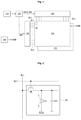
- FIG. 1 is a block diagram schematically showing an LCD device.
- FIG. 2 is a circuit diagram schematically showing a sub-pixel shown in FIG. 1 .
- FIG. 3 is a block diagram schematically showing an OLED device.
- FIG. 4 is a diagram schematically showing a configuration of a sub-pixel shown in FIG. 3 .
- FIGS. 5A and 5B are diagrams showing examples of arrangement of scan drivers in a gate-in-panel structure.
- FIG. 6 is a diagram illustrating a first configuration of a device related to the scan drivers in a gate-in-panel structure.
- FIG. 7 is a diagram illustrating a second configuration of a device related to the scan drivers in a gate-in-panel structure.
- FIG. 8 is a diagram showing a part of a shift register according to an experimental example of the disclosure.
- FIG. 9 is a diagram showing node voltages and output waveforms of the shift register shown in FIG. 8 .
- FIGS. 10 and 11 are diagrams for description related to output buffers of the shift register shown in FIG. 8 .
- FIG. 12 is a diagram showing a part of a shift register according to a first embodiment of the disclosure.
- FIG. 13 is a diagram showing node voltages and output waveforms of the shift register shown in FIG. 12 .
- FIGS. 14 and 15 are diagrams for description related to output buffers of the shift register shown in FIG. 12 .
- FIG. 16 is a diagram for comparatively describing differences between the experimental example and the first embodiment.
- FIG. 17 is a diagram showing a shift register according to a second embodiment of the disclosure.
- FIG. 18 is a diagram showing node voltages and output waveforms of the shift register shown in FIG. 17 .
- FIG. 19 is a diagram showing a shift register according to a third embodiment of the disclosure.
- FIG. 20 is a diagram showing node voltages and output waveforms of the shift register shown in FIG. 19 .
- QDD quantum dot display
- LCD liquid crystal display
- OLED organic light emitting display
- PDP plasma display panel
- the LCD or the OLED includes a display panel having a plurality of sub-pixels, a driver which outputs driving signals for driving the display panel, and a power supply which generates power to be supplied to the display panel and the driver.
- the driver includes a scan driver which provides scan signals (or gate signals) to the display panel and a data driver which provides data signals to the display panel.
- the aforementioned display device can display images in such a manner that selected sub-pixels transmit light or directly emit light when driving signals, for example, scan signals and data signals are provided to sub-pixels formed on the display panel.
- a thin film transistor is a three-electrode element including a gate, a source and a drain.
- the source is an electrode that supplies carriers to the transistor. Carriers flow from the source in the thin film transistor.
- the drain is an electrode from which carries flow to the outside of the thin film transistor. That is, carriers flow from the source to the drain in the thin film transistor.
- a source voltage is lower than a drain voltage such that electrons can flow from the source to the drain because the electrons are carriers. Since electrons flow from the source to the drain in the n-type thin film transistor, current flows from the drain to the source.
- a source voltage is higher than a drain voltage such that holes can flow from the source to the drain because the holes are carriers. Since holes flow from the source to the drain in the p-type thin film transistor, current flows from the source to the drain.
- the source and the drain of the thin film transistor may be switched according to an applied voltage. In view of this, one of the source and drain will be described as a first electrode and the other will be described as a second electrode in the following description.
- FIG. 1 is a block diagram schematically showing an LCD device and FIG. 2 is a circuit diagram schematically showing a sub-pixel shown in FIG. 1 .
- the LCD device includes an image provider 110 , a timing controller 120 , a scan driver 130 , a data driver 140 , a liquid crystal panel 150 , a back light unit 170 and a power supply 180 .
- the image provider 110 outputs various driving signals along with an image data signal supplied from the outside or an image data signal stored in an internal memory.
- the image provider 110 provides the data signal and the various driving signals to the timing controller 120 .
- the timing controller 120 outputs a gate timing control signal GDC for controlling an operation timing of the scan driver 130 , a data timing control signal DDC for controlling an operation timing of the data driver 140 , and various synchronization signals (a vertical synchronization signal Vsync and a horizontal synchronization signal Hsync).
- the timing controller 120 provides the data signal (or a data voltage) DATA supplied from the image provider 110 along with the data timing control signal DDC to the data driver 140 .
- the timing controller 120 may be configured in the form of an integrated circuit (IC) and mounted on a printed circuit board, the disclosure is not limited thereto.
- the scan driver 130 outputs a scan signal (or a gate signal) in response to the gate timing control signal GDC supplied from the timing controller 120 .
- the scan driver 130 provides the scan signal to sub-pixels included in the liquid crystal panel 150 through gate lines GL 1 to GLm.
- the scan driver 130 may be configured in the form of an IC or may be directly formed on the liquid crystal panel 150 in a gate-in-panel structure, but the disclosure is not limited thereto.
- the data driver 140 samples and latches the data signal DATA in response to the data timing control signal DDC supplied from the timing controller 120 , converts the digital data signal into an analog data signal on the basis of a gamma reference voltage and outputs the analog data signal.
- the data driver 140 provides data voltages to the sub-pixels included in the liquid crystal panel 150 through data lines DL 1 to DLn.
- the data driver 140 may be configured in the form of an IC and mounted on the display panel 150 or mounted on a printed circuit board, but the disclosure is not limited thereto.
- the power supply 180 generates a common voltage VCOM on the basis of an external input voltage supplied from the outside and outputs the common voltage VCOM.
- the power supply 180 can generate and output voltages (e.g., a scan high voltage and a scan low voltage) sufficient to drive the scan driver 130 and voltages (e.g., a drain voltage and a half drain voltage) sufficient to drive the data driver 140 as well as the common voltage VCOM.
- the liquid crystal panel 150 displays an image in response to scan signals supplied from the scan driver 130 , data voltages supplied from the data driver 140 and the common voltage VCOM supplied from the power supply 180 .
- the sub-pixels of the liquid crystal panel 150 control light provided through the back light unit 170 .
- one sub-pixel SP includes a switching transistor SW, a storage capacitor Cst and a liquid crystal layer Clc.
- the gate electrode of the switching transistor SW is connected to a scan line GL 1 and the source electrode thereof is connected to a data line DL 1 .
- One terminal of the storage capacitor Cst is connected to the drain electrode of the switching transistor SW and the other terminal thereof is connected to a common voltage line Vcom.
- the liquid crystal layer Clc is formed between a pixel electrode 1 connected to the drain electrode of the switching transistor SW and a common electrode 2 connected to the common voltage line Vcom.
- the liquid crystal panel 150 is realized in a twisted nematic (TN) mode, a vertical alignment (VA) mode, an in-plane switching (IPS) mode, a fringe field switching (FFS) mode or an electrically controlled birefringence (ECB) mode according to structures of the pixel electrode 1 and the common electrode 2 .
- TN twisted nematic
- VA vertical alignment
- IPS in-plane switching
- FFS fringe field switching
- EBC electrically controlled birefringence
- the back light unit 170 provides light to the liquid crystal panel 150 using a light source that emits light.
- the back light unit 170 may include a light-emitting diode (LED) driver which drives LEDs, an LED substrate on which LEDs are mounted, a light guide plate which converts light emitted from LEDs into surface light, a reflector which reflects light under the light guide plate, and optical sheets which condense and spread light emitted from the light guide plate, the disclosure is not limited thereto.
- LED light-emitting diode
- FIG. 3 is a block diagram schematically showing an OLED device and FIG. 4 is a diagram schematically showing a configuration of a sub-pixel shown in FIG. 3 .
- the OLED device includes an image provider 110 , a timing controller 120 , a scan driver 130 , a data driver 140 , a display panel 150 and a power supply 170 .
- the power supply 180 generates a first power voltage EVDD that is a high voltage and a second power voltage EVSS that is a low voltage on the basis of an external input voltage supplied from the outside and outputs the first power voltage EVDD and the second power voltage EVSS.
- the power supply 180 can generate and output voltages (e.g., a scan high voltage and a scan low voltage) sufficient to drive the scan driver 130 and voltages (e.g., a drain voltage and a half drain voltage) sufficient to drive the data driver 140 as well as the first and second power voltages EVDD and EVSS.
- the display panel 150 displays an image in response to scan signals and data voltages output from drivers including the scan driver 130 and the data driver 140 and the first and second power voltages EVDD and EVSS output from the power supply 180 . Sub-pixels of the display panel 150 directly emit light.
- one sub-pixel SP includes a switching transistor SW and a pixel circuit PC including a driving transistor, a storage capacitor and an OLED.
- the sub-pixel SP used in the OLED device directly emits light and thus has a complicated circuit configuration compared to LCDs. Furthermore, not only an OLED emitting light but also a compensation circuit for compensating for deterioration of a driving transistor that supplies driving current to the OLED are configured in complicated and various manners. Accordingly, the pixel circuit PC included in the sub-pixel SP is shown in the form of a block.
- FIGS. 5A and 5B are diagrams showing examples of arrangement of scan drivers in a gate-in-panel structure
- FIG. 6 is a diagram illustrating a first configuration of a device related to the scan drivers in a gate-in-panel structure
- FIG. 7 is a diagram illustrating a second configuration of a device related to the scan drivers in a gate-in-panel structure.
- scan drivers 130 a and 130 b in a gate-in-panel structure are disposed in non-display areas of the display panel 150 .
- the scan drivers 130 a and 130 b can be disposed in left and right non-display areas NA of the display panel 150 , as shown in FIG. 5A .
- the scan drivers 150 a and 150 b may be disposed in upper and lower non-display areas NA of the display panel 150 , as shown in FIG. 5B .
- a pair of scan drivers 130 a and 130 b are disposed in non-display areas NA located on the left and right or the upper and lower sides of a display area AA
- the disclosure is not limited thereto and a single scan driver may be disposed in a non-display area NA located on the left, right, upper or lower side of the display area AA.
- the scan driver 130 in a gate-in-panel structure may include a shift register 131 and a level shifter 135 .
- the level shifter 135 generates a plurality of clock signals GCLK on the basis of signals output from the timing controller 120 and outputs the clock signals GCLK.
- the plurality of clock signals GCLK is generated to have N different phases (N is an integer equal to or greater than 2) such as 2 phases, 4 phases or 8 phases.
- the shift register 131 operates on the basis of the plurality of clock signals GCLK output from the level shifter 135 and outputs signals Scan 1 to Scan m that can turn transistors formed on the display panel on or off.
- the shift register 131 includes a plurality of stages.
- the plurality of stages has a cascaded structure and receives an output signal of at least one preceding or following stage as an input signal.
- One stage outputs at least one signal.
- Scan 1 corresponds to a signal output from a first stage
- Scan m corresponds to a signal output from an m-th stage.
- the level shifter 135 is configured in the form of an IC, whereas the shift register 131 is configured in the form of a thin film in a gate-in-panel structure. That is, a part of the scan driver 130 which is formed on the display panel is the shift register 131 ( 130 a and 130 b in FIGS. 5A and 5B corresponds to 131 ).
- the level shifter 135 is configured in the form of an IC. Accordingly, the level shifter 135 can be configured in the form of a separate IC as shown in FIG. 6 and may be included in the power supply 180 , as shown in FIG. 7 .
- FIG. 8 is a diagram showing a part of a shift register according to an experimental example of the disclosure
- FIG. 9 is a diagram showing node voltages and output waveforms of the shift register shown in FIG. 8
- FIGS. 10 and 11 are diagrams for description related to output buffers of the shift register shown in FIG. 8 .
- the shift register 131 includes a node controller 132 and an output circuit 134 .
- the node controller 132 serves to control charging/discharging of a Q node Q and a QB node QB of the output circuit 134 .
- the output circuit 134 serves to output a carry signal C[n] along with scan signals Scouta[n] and Scoutb[n] in response to electric potentials of the Q node Q and the QB node QB.
- the output circuit 134 includes first buffer transistors T 6 A and T 7 A that output the first scan signal Scouta[a], second buffer transistors T 6 B and T 7 B that output the second scan signal Scoutb[n], and third buffer transistors T 6 cr and T 7 cr that output the carry signal C[n].
- the first buffer transistors T 6 A and T 7 A output the first scan signal Scouta[n] on the basis of a first clock signal applied through a first clock signal line SCCLKA[n] and a first low voltage applied through a first low voltage line GVSS 0 .
- the first buffer transistors T 6 A and T 7 A are turned on/off in response to electric potentials charged/discharged to/from the Q node Q and the QB node QB.
- the first buffer transistors T 6 A and T 7 A include a first pull-up transistor T 6 A turned on in response to the electric potential of the Q node Q and a first pull-down transistor T 7 A turned on in response to the electric potential of the QB node QB.
- the second buffer transistors T 6 B and T 7 B output the second scan signal Scoutb[n] on the basis of a second clock signal applied through a second clock signal line SCCLKB[n] and the first low voltage applied through the first low voltage line GVSS 0 .
- the second buffer transistors T 6 B and T 7 B are turned on/off in response to electric potentials charged/discharged to/from the Q node Q and the QB node QB.
- the second buffer transistors T 6 B and T 7 B include a second pull-up transistor T 6 B turned on in response to the electric potential of the Q node Q and a second pull-down transistor T 7 B turned on in response to the electric potential of the QB node QB.
- the third buffer transistors T 6 cr and T 7 cr output the carry signal C[n] on the basis of a third clock signal applied through a third clock signal line SRCLK[n] and a second or third low voltage applied through a second or third low voltage line GVSS 1 or GVSS 2 .
- the third buffer transistors T 6 cr and T 7 cr are turned on/off in response to electric potentials charged/discharged to/from the Q node Q and the QB node QB.
- the third buffer transistors T 6 cr and T 7 cr include a third pull-up transistor T 6 cr turned on in response to the electric potential of the Q node Q and a third pull-down transistor T 7 cr turned on in response to the electric potential of the QB node QB.
- capacitors Cb and Cc for stably maintaining output of the carry signal C[n] are provided to the output terminals of the third buffer transistors T 6 cr and T 7 cr is illustrated.
- “Cb” serves to perform carry boosting (bootstrapping) for stable output of the carry signal
- “Cc” serves to maintain the output for stable output of the carry signal.
- the capacitors Cb and Cc may also be included in the first buffer transistors T 6 A and T 7 A or the second buffer transistors T 6 B and T 7 B, and the disclosure is not limited to the configuration shown in the figure.
- the first to third pull-up transistors T 6 A, T 6 B and T 6 cr of the shift register 131 output the carry signal C[n] along with the logic high scan signals Scouta[n] and Scoutb[n] on the basis of the clock signals.
- the output duration of the carry signal C[n] is longer than those of the first second scan signal Scouta[n] and the second scan signal Scoutb[n]. In this case, if the boost capacitor Cb for carry boosting is provided between the gate electrode and the source electrode of the third pull-up transistor T 6 cr , the carry signal C[n] can be stably output.
- the first scan signal Scouta[n] and the second scan signal Scoutb[n] are output overlapping for the output duration of the carry signal C[n].
- the first scan signal Scouta[n] is output before the second scan signal Scoutb[n], and output is performed in a state in which the charged electric potential of the Q node Q is sufficient.
- a buffer driving voltage difference can be reduced, an output deviation can be decreased and output signal falling time can be optimized.
- FIG. 12 is a diagram showing a part of a shift register according to a first embodiment of the disclosure
- FIG. 13 is a diagram showing node voltages and output waveforms of the shift register shown in FIG. 12
- FIGS. 14 and 15 are diagrams for description related to output buffers of the shift register shown in FIG. 12
- FIG. 16 is a diagram for comparatively describing differences between the experimental example and the first embodiment.
- the shift register 131 includes a node controller 132 and an output circuit 134 .
- the node controller 132 serves to control charging/discharging of a Q node Q and a QB node QB of the output circuit 134 .
- the output circuit 134 serves to output a carry signal C[n] along with scan signals Scouta[n] and Scoutb[n] in response to electric potentials of the Q node Q and the QB node QB.
- the output circuit 134 includes first buffer transistors T 6 A, T 7 A and T 6 C that output the first scan signal Scouta[a], second buffer transistors T 6 B and T 7 B that output the second scan signal Scoutb[n], and third buffer transistors T 6 cr and T 7 cr that output the carry signal C[n].
- the first buffer transistors T 6 A, T 7 A and T 6 C output the first scan signal Scouta[n] on the basis of a first clock signal applied through a first clock signal line SCCLKA[n] and a first low voltage applied through a first low voltage line GVSS 0 .
- the first buffer transistors T 6 A, T 7 A and T 6 C are turned on/off in response to electric potentials charged/discharged to/from the Q node Q and the QB node QB.
- the first buffer transistors T 6 A, T 7 A and T 6 C include a first pull-up transistor T 6 A turned on in response to the electric potential of the Q node Q, a first dummy buffer transistor T 6 C, and a first pull-down transistor T 7 A turned on in response to the electric potential of the QB node QB.
- the second buffer transistors T 6 B and T 7 B output the second scan signal Scoutb[n] on the basis of a second clock signal applied through a second clock signal line SCCLKB[n] and the first low voltage applied through the first low voltage line GVSS 0 .
- the second buffer transistors T 6 B and T 7 B are turned on/off in response to electric potentials charged/discharged to/from the Q node Q and the QB node QB.
- the second buffer transistors T 6 B and T 7 B include a second pull-up transistor T 6 B turned on in response to the electric potential of the Q node Q and a second pull-down transistor T 7 B turned on in response to the electric potential of the QB node QB.
- the third buffer transistors T 6 cr and T 7 cr output the carry signal C[n] on the basis of a third clock signal applied through a third clock signal line SRCLK[n] and a second or third low voltage applied through a second or third low voltage line GVSS 1 or GVSS 2 .
- the third buffer transistors T 6 cr and T 7 cr are turned on/off in response to electric potentials charged/discharged to/from the Q node Q and the QB node QB.
- the third buffer transistors T 6 cr and T 7 cr include a third pull-up transistor T 6 cr turned on in response to the electric potential of the Q node Q and a third pull-down transistor T 7 cr turned on in response to the electric potential of the QB node QB.
- capacitors Cb and Cc for stably maintaining output of the carry signal C[n] are provided to the output terminals of the third buffer transistors T 6 cr and T 7 cr is illustrated.
- “Cb” serves to perform carry boosting (bootstrapping) for stable output of the carry signal
- “Cc” serves to maintain the output for stable output of the carry signal.
- the capacitors Cb and Cc may also be included in the first buffer transistors T 6 A and T 7 A or the second buffer transistors T 6 B and T 7 B, and the disclosure is not limited to the configuration shown in the figure.
- the first to third pull-up transistors T 6 A, T 6 B and T 6 cr of the shift register 131 output the carry signal C[n] along with the logic high scan signals Scouta[n] and Scoutb[n] on the basis of the clock signals.
- the output duration of the carry signal C[n] is longer than those of the first second scan signal Scouta[n] and the second scan signal Scoutb[n]. In this case, if the boost capacitor Cb for carry boosting is provided between the gate electrode and the source electrode of the third pull-up transistor T 6 cr , the carry signal C[n] can be stably output.
- the first scan signal Scouta[n] and the second scan signal Scoutb[n] are output overlapping for the output duration of the carry signal C[n].
- the first scan signal Scouta[n] is output before the second scan signal Scoutb[n], and output is performed in a state in which the charged electric potential of the Q node Q is sufficient.
- a buffer driving voltage difference can be reduced, an output deviation can be decreased and output signal falling time can be optimized.
- the shift register 131 includes the first dummy buffer transistor T 6 C that is turned on in response to the Q node Q and has a first electrode commonly connected to the first clock signal line SCCLKA[n] like the first pull-up transistor T 6 A.
- the first dummy buffer transistor T 6 C serves to eliminate a parasitic capacitance (or TFT Cap) deviation between the first pull-up transistor T 6 A and the second pull-up transistor T 6 B under the condition of “first pull-up transistor T 6 A ⁇ second pull-up transistor T 6 B”. That is, the first dummy buffer transistor T 6 C serves to adjust parasitic capacitances existing in the two output buffers to be similar/identical and thus may be defined as a first compensation transistor.
- the width of the channel region of the first pull-up transistor T 6 A is defined as “Buffer A”
- the width of the channel region of the second pull-up transistor T 6 B is defined as “Buffer B”
- the width of the channel region of the first dummy buffer transistor T 6 C is defined as “Buffer C”
- a relationship among the widths of the channel regions can be represented as “Buffer A+C (compensation) Buffer B”.
- “Buffer A+C (compensation) ⁇ Buffer B” may be defined as a relationship among parasitic capacitances of the corresponding transistors and then re-defined as “A+C ⁇ B”.
- “ ⁇ ” means “approximately the same”, “almost the same” or “similar” and may be represented as “ ⁇ ”.
- the first dummy buffer transistor T 6 C such that it forms a predetermined compensation capacitor in order to execute a function as a compensation transistor as described above.
- the first dummy buffer transistor T 6 C can have the same channel region width in all stages, the first dummy buffer transistor T 6 C may be formed to have different channel region widths for stage groups each having K (K is an integer equal to or greater than 2) stages for fine compensation of output deviations.
- K is an integer equal to or greater than 2 stages for fine compensation of output deviations.
- the width of the channel region of the first dummy buffer transistor T 6 C is less than and does not exceed the width of the channel region of the first pull-up transistor T 6 A or the second pull-up transistor T 6 B.
- a bootstrapped voltage is reflected in the charged electric potential of the Q node Q[n] but the electric potential decreases according to falling of the first clock signal in a period T 2 following a period T 1 in the experimental example.
- a bootstrapped voltage is reflected in the charged electric potential of the node Q[n] and the electric potential does not decrease according to falling of the first clock signal and is maintained even in the periods T 1 and T 2 in the first embodiment.
- an output deviation is higher in the experimental example than in the first embodiment even if a design for eliminating an output deviation of the scan driver in the middle of the display panel (middle point on the basis of pixels in the vertical lines) is employed.
- the output deviation is lower in the first embodiment than in the experimental example even if a design for eliminating an output deviation of the scan driver in the middle of the display panel (middle point on the basis of pixels in the vertical lines) is employed.
- the first embodiment can improve a falling time deviation in output signals by position which can be caused by different designs of output buffers.
- the first embodiment can compensate for a parasitic capacitance deviation between clock signal lines and thus can solve a node charging problem which can be caused by a parasitic capacitance deviation between output buffers.
- the first embodiment can minimize the influence of a load between clock signal lines using the compensation function of the dummy transistor.
- compensation design can be performed within a range in which a bezel area is not increased because compensation is performed in the output buffer stage in the first embodiment.
- FIG. 17 is a diagram showing a shift register according to a second embodiment of the disclosure
- FIG. 18 is a diagram showing node voltages and output waveforms of the shift register shown in FIG. 17
- FIG. 19 is a diagram showing a shift register according to a third embodiment of the disclosure
- FIG. 20 is a diagram showing node voltages and output waveforms of the shift register shown in FIG. 19 .
- the shift register 131 includes a node controller 132 , a reset circuit 133 and an output circuit 134 .
- the shift register 131 operates on the basis of a first clock signal Scclka, a second clock signal Scclkb, a third clock signal Crclk, a first high voltage, first to third high voltages, an (N ⁇ 2)-th carry signal C[n ⁇ 2], an (N+2)-th carry signal C[n+2].
- the first clock signal Scclka and the second clock signal Scclkb are applied in such a manner that logic high periods thereof partially overlap.
- the third clock signal Crclk is applied in such a manner that it overlaps both the logic high periods of the first and second clock signals Scclka and Scclkb.
- Carry signals are applied in the form of pulses in which logic high periods sequentially occur without overlapping because two preceding and following stages are used.
- the node controller 132 serves to control charging and discharging of the Q node Q and the QB node QB of the output circuit 134 .
- the reset circuit 133 serves to reset the QB node QB.
- the output circuit 134 serves to output a carry signal C[n] along with scan signals Scouta[n] and Scoutb[n] in response to electric potentials of the Q node Q and the QB node QB.
- the node controller 132 includes a first transistor T 1 , a 1A-th transistor T 1 A, a third transistor T 3 , a 3A-th transistor T 3 A, a 3n-th transistor T 3 n , a 3nA-th transistor T 3 n A, a 3q-th transistor T 3 q , a fourth transistor T 4 , a 4l-th transistor T 4 l , a 4q-th transistor T 4 q , a fifth transistor T 5 , and a 5q-th transistor T 5 q.
- a gate electrode and a first electrode of the first transistor T 1 are commonly connected to a (N ⁇ 2)-th carry signal line C[n ⁇ 2], and a second electrode thereof is connected to a Qh node Qh.
- the first transistor T 1 is turned on by the (N ⁇ 2)-th carry signal applied through the (N ⁇ 2)-th carry signal line C[n ⁇ 2] and serves to transfer the (N ⁇ 2)-th carry signal to the Qh node Qh.
- a gate electrode of the 1A-th transistor T 1 A is connected to the (N ⁇ 2)-th carry signal line C[n ⁇ 2], a first electrode thereof is connected to the second electrode of the first transistor T 1 , and a second electrode thereof is connected to Q node Q.
- the 1A-th transistor T 1 A is turned on by the (N ⁇ 2)-th carry signal applied through the (N ⁇ 2)-th carry signal line C[n ⁇ 2] and serves to charge the Q node Q on the basis of the (N ⁇ 2)-th carry signal.
- a gate electrode of the third transistor T 3 is connected to the QB node QB, a first electrode thereof is connected to the Q node Q, and a second electrode thereof is connected to the first electrode of the 3A-th transistor T 3 A.
- the third transistor T 3 is turned on in response to the electric potential of the QB node QB and serves to discharge the Q node Q to a third low voltage of a third low voltage line GVSS 2 along with the 3A-th transistor T 3 A.
- a gate electrode of the 3A-th transistor T 3 A is connected to the QB node QB, a first electrode thereof is connected to the second electrode of the third transistor T 3 , and a second electrode thereof is connected to the third low voltage line GVSS 2 .
- the 3A-th transistor T 3 A is turned on in response to the electric potential of the QB node QB and serves to discharge the Q node Q to the third low voltage of the third low voltage line GVSS 2 along with the third transistor T 3 .
- a gate electrode of the 3n-th transistor T 3 n is connected to an (N+2)-th carry signal line C[n+2], a first electrode thereof is connected to the Q node Q, and a second electrode thereof is connected to a first electrode of the 3nA-th transistor TnA.
- the 3n-th transistor T 3 n is turned on by an (N+2)-th carry signal applied through the (N+2)-th carry signal line C[n+2] and serves to discharge the Q node Q to the third low voltage of the third low voltage line GVSS 2 along with the 3nA-th transistor T 3 n A.
- a gate electrode of the 3nA-th transistor T 3 n A is connected to the (N+2)-th carry signal line C[n+2], a first electrode thereof is connected to the second electrode of the 3n-th transistor T 3 n , and a second electrode thereof is connected to the third low voltage line GVSS 2 .
- the 3nA-th transistor T 3 n A is turned on by the (N+2)-th carry signal applied through the (N+2)-th carry signal line C[n+2] and serves to discharge the Q node Q to the third low voltage of the third low voltage line GVSS 2 along with the 3n-th transistor T 3 n.
- a gate electrode of the 3q-th transistor T 3 q is connected to Q node Q, a first electrode thereof is connected to a first high voltage line GVDD, and a second electrode thereof is connected to the Qh node Qh.
- the 3q-th transistor T 3 q is turned on in response to the electric potential of the Q node Q and serves to transfer the first high voltage of the first high voltage line GVDD to the Qh node Qh.
- a gate electrode of the fourth transistor T 4 is connected to one terminal of a first capacitor Ca and a second electrode of the 4l-th transistor T 4 l , a first electrode thereof is connected to the first high voltage line GVDD, and a second electrode thereof is connected to the other terminal of the first capacitor Ca and the QB node QB.
- the fourth transistor T 4 is turned on by the first high voltage transferred through the 4l-th transistor T 4 l and serves to charge the QB node QB with the first high voltage of the first high voltage line GVDD.
- the first capacitor Ca serves to generate a bootstrapping voltage at the gate node of the fourth transistor T 4 .
- a gate electrode and a first electrode of the 4l-th transistor T 4 l are connected to the first high voltage line GVDD and a second electrode thereof is connected to the gate electrode of the fourth transistor T 4 and the first electrode of the 4q-th transistor T 4 q .
- the 4l-th transistor T 4 l is turned on by the first high voltage and serves to transfer the first high voltage of the first high voltage line GVDD to the gate node of the fourth transistor T 4 .
- a gate electrode of the 4q-th transistor T 4 q is connected to the Q node Q, a first electrode thereof is connected to the gate electrode of the fourth transistor T 4 and the second electrode of the 4l-th transistor T 4 l , and a second electrode thereof is connected to a second low voltage line GVSS 1 .
- the 4q-th transistor T 4 q is turned on in response to the electric potential of the Q node Q and serves to transfer the second low voltage of the second low voltage line GVSS 1 to the gate node of the fourth transistor T 4 (to discharge the gate node of T 4 ).
- a gate electrode of the fifth transistor T 5 is connected to the (N ⁇ 2)-th carry signal line C[n ⁇ 2], a first electrode thereof is connected to the QB node QB, and a second electrode thereof is connected to the third low voltage line GVSS 2 .
- the fifth transistor T 5 is turned on by the (N ⁇ 1)-th carry signal of the (N ⁇ 2)-th carry signal line C[n ⁇ 2] and serves to discharge the QB node QB to the third low voltage of the third low voltage line GVSS 2 .
- a gate electrode of the 5q-th transistor T 5 l is connected to the Q node Q, a first electrode thereof is connected to the second electrode of the fourth transistor T 4 , one terminal of the first capacitor Ca and the QB node QB, and a second electrode thereof is connected to the third low voltage line GVSS 2 .
- the 5q-th transistor T 5 q is turned on in response to the electric potential of the Q node Q and serves to discharge the QB node QB to the third low voltage of the third low voltage line GVSS 2 .
- the reset circuit 133 includes at least one of a 5A-th transistor T 5 A and a 5B-th transistor T 5 B.
- the 5B-th transistor T 5 B may be omitted in the reset circuit 133 .
- a gate electrode of the 5A-th transistor T 5 A is connected to a reset signal line RST, a first electrode thereof is connected to the QB node QB, and a second electrode thereof is connected to a first electrode of the 5B-th transistor T 5 B.
- the 5A-th transistor T 5 A is turned on by a reset signal of the reset signal line RST and serves to reset the QB node QB to the third low voltage of the third low voltage line GVSS 2 along with the 5B-th transistor T 5 B.
- a gate electrode of the 5B-th transistor TSB is connected to a node M (node M can be normally selected as a node to which a carry signal is transferred although it depends on the design of the node controller), a first electrode thereof is connected to the second electrode of the 5A-th transistor TSA, and a second electrode thereof is connected to the third low voltage line GVSS 2 .
- the 5B-th transistor TSB is turned on in response to the electric potential of the node M and serves to reset the QB node QB to the third low voltage of the third low voltage line GVSS 2 along with the 5A-th transistor TSA.
- the output circuit 134 includes first buffer transistors T 6 A, T 6 A and T 6 C that output the first scan signal Scouta[b], second buffer transistors T 6 B and T 7 B that output the second scan signal Scoutb[n], and third buffer transistors T 6 cr and T 7 cr that output a carry signal C[n].
- the first buffer transistors T 6 A and T 7 A include a first pull-up transistor T 6 A turned on in response to the electric potential of the Q node Q and a first pull-down transistor T 7 A turned on in response to the electric potential of the QB node QB.
- a gate electrode of the first pull-up transistor T 6 A is connected to the Q node Q, a first electrode thereof is connected to a first clock signal line SCCLKA[n], and a second electrode thereof is connected to a first output terminal SCOUTA[n].
- a gate electrode of the first pull-down transistor T 7 A is connected to the QB node QB, a first electrode thereof is connected to the first output terminal SCOUTA[n], and a second electrode thereof is connected to the first low voltage line GVSS 0 .
- the first buffer transistors T 6 A and T 7 A output a first scan signal Scouta[n] on the basis of a first clock signal applied through the first clock signal line SCCLKA[n] and the first low voltage applied through the first low voltage line GVSS 0 .
- the second buffer transistors T 6 B and T 7 B include a second pull-up transistor T 6 B turned on in response to the electric potential of the Q node Q and a second pull-down transistor T 7 B turned on in response to the electric potential of the QB node QB.
- a gate electrode of the second pull-up transistor T 6 B is connected to the Q node Q, a first electrode thereof is connected to a second clock signal line SCCLKB[n], and a second electrode thereof is connected to a second output terminal SCOUTB[n].
- a gate electrode of the second pull-down transistor T 7 B is connected to the QB node QB, a first electrode thereof is connected to the second output terminal SCOUTB[n], and a second electrode thereof is connected to the first low voltage line GVSS 0 .
- the second buffer transistors T 6 B and T 7 B output the second scan signal Scoutb[n] on the basis of a second clock signal applied through the second clock signal line SCCLKB[n] and the first low voltage applied through the first low voltage line GV
- the third buffer transistors T 6 cr and T 7 cr include a third pull-up transistor T 6 cr turned on in response to the electric potential of the Q node Q and a third pull-down transistor T 7 cr turned on in response to the electric potential of the QB node QB.
- a gate electrode of the third pull-up transistor T 6 cr is connected to the Q node Q and one terminal of a second capacitor Cb (boosting capacitor), a first electrode thereof is connected to a third clock signal line SRCLK[n], and a second electrode thereof is connected to a third output terminal C[n], the other terminal of the second capacitor Cb and one terminal of a third capacitor Cc.
- a gate electrode of the third pull-down transistor T 7 cr is connected to the QB node QB, a first electrode thereof is connected to the third output terminal C[n] and one terminal of the third capacitor Cc, and a second electrode thereof is connected to the third low voltage line GVSS 2 and the other terminal of the third capacitor Cc.
- the third buffer transistors T 6 cr and T 7 cr output the carry signal C[n] on the basis of a third clock signal applied through the third clock signal line SRCLK[n] and the third low voltage applied through the third low voltage line GVSS 2 .
- the second embodiment includes the first dummy buffer transistor T 6 C with one electrode floating in order to eliminate a parasitic capacitance (or TFT Cap) deviation between the first pull-up transistor T 6 A and the second pull-up transistor T 6 B when output buffers are designed such that their channel regions have different widths under the condition such as “first pull-up transistor T 6 A ⁇ second pull-up transistor T 6 B”.
- the first dummy buffer transistor T 6 C serves to compensate for a shortage of parasitic capacitance for the first pull-up transistor T 6 A. While a gate electrode of the first dummy buffer transistor T 6 C is connected to the Q node Q and a first electrode thereof is connected to the first clock signal line SCCLKA[n], the second electrode of the first dummy buffer transistor T 6 C remains in a floating state.
- the width of the channel region of the first pull-up transistor T 6 A is defined as “Buffer A”
- the width of the channel region of the second pull-up transistor T 6 B is defined as “Buffer B”
- the width of the channel region of the first dummy buffer transistor T 6 C is defined as “Buffer C”
- a relationship among the widths of the channel regions can be represented as “Buffer A+C (compensation) Buffer B”.
- the first dummy buffer transistor T 6 C is formed to have a common gate and common drain connection structure with the first pull-up transistor T 6 A and a source (source electrode) in a floating state in order to execute a function as a compensation transistor (form a compensation capacitor) as described above.
- the shift register 131 according to the third embodiment includes a node controller 132 , a reset circuit 133 and an output circuit 134 .
- the first dummy buffer transistor T 6 C has different configurations and the shift registers 131 according to the second and third embodiments are substantially the same. Accordingly, the part related to the first dummy buffer transistor T 6 C is described and the second embodiment is referred to for the remaining part.
- the third embodiment includes a first dummy buffer transistor T 6 C that is diode-connected in order to eliminate a parasitic capacitance (or TFT Cap) deviation between the first pull-up transistor T 6 A and the second pull-up transistor T 6 B when output buffers are designed such that their channel regions have different widths under the condition such as “first pull-up transistor T 6 A ⁇ second pull-up transistor T 6 B”.
- the first dummy buffer transistor T 6 C serves to compensate for a shortage of parasitic capacitance for the first pull-up transistor T 6 A.
- a gate electrode of the first dummy buffer transistor T 6 C is connected to the Q node Q and first and second electrodes thereof are connected to the first clock signal line SCCLKA[n] such that the first dummy buffer transistor T 6 C is in a diode connection state.
- the width of the channel region of the first pull-up transistor T 6 A is defined as “Buffer A”
- the width of the channel region of the second pull-up transistor T 6 B is defined as “Buffer B”
- the width of the channel region of the first dummy buffer transistor T 6 C is defined as “Buffer C”
- a relationship among the widths of the channel regions can be represented as “Buffer A+(Buffer C (compensation)) ⁇ 2 ⁇ Buffer B”.
- the first dummy buffer transistor T 6 C is formed to be in a diode connection structure in which the first dummy buffer transistor T 6 C has a common gate and a common drain with the first pull-up transistor T 6 A and a source (source electrode) connected to the drain (drain electrode) in order to execute a function as a compensation transistor (form a compensation capacitor) as described above.
- the disclosure can solve a problem of falling time deviation in output signals by position which can be caused when output buffers of a shift register are designed such that their channel regions have different widths.
- the disclosure can compensate for a parasitic capacitance deviation between clock signal lines of the shift register and thus can solve a node charging problem that can be caused by a parasitic capacitance deviation in output buffers.
- the disclosure can minimize the influence of a load between clock signal lines according to the compensation function of the dummy transistor added to the shift register.
- the disclosure can execute a compensation design within a range in which a bezel area is not increased because compensation is performed in an output buffer stage of the shift register.
Landscapes
- Engineering & Computer Science (AREA)
- Physics & Mathematics (AREA)
- Computer Hardware Design (AREA)
- General Physics & Mathematics (AREA)
- Theoretical Computer Science (AREA)
- Chemical & Material Sciences (AREA)
- Crystallography & Structural Chemistry (AREA)
- Control Of Indicators Other Than Cathode Ray Tubes (AREA)
- Liquid Crystal Display Device Control (AREA)
- Shift Register Type Memory (AREA)
Applications Claiming Priority (2)
| Application Number | Priority Date | Filing Date | Title |
|---|---|---|---|
| KR1020180121868A KR102522804B1 (ko) | 2018-10-12 | 2018-10-12 | 시프트 레지스터 및 이를 이용한 표시장치 |
| KR10-2018-0121868 | 2018-10-12 |
Publications (2)
| Publication Number | Publication Date |
|---|---|
| US20200118509A1 US20200118509A1 (en) | 2020-04-16 |
| US11244644B2 true US11244644B2 (en) | 2022-02-08 |
Family
ID=70160294
Family Applications (1)
| Application Number | Title | Priority Date | Filing Date |
|---|---|---|---|
| US16/599,810 Active 2040-04-24 US11244644B2 (en) | 2018-10-12 | 2019-10-11 | Shift register and display device using the same |
Country Status (3)
| Country | Link |
|---|---|
| US (1) | US11244644B2 (zh) |
| KR (1) | KR102522804B1 (zh) |
| CN (1) | CN111048025B (zh) |
Families Citing this family (12)
| Publication number | Priority date | Publication date | Assignee | Title |
|---|---|---|---|---|
| FR3092685B1 (fr) * | 2019-02-11 | 2021-07-02 | Isorg | Système de reconnaissance d’empreinte digitale équipé d’un dispositif amélioré d’adressage de lignes |
| CN111445830B (zh) * | 2020-04-23 | 2021-09-03 | 深圳市华星光电半导体显示技术有限公司 | 驱动电路及显示装置 |
| CN113674708B (zh) * | 2020-05-14 | 2023-04-11 | 京东方科技集团股份有限公司 | 移位寄存器、栅极驱动电路、显示装置及其驱动方法 |
| CN111599315B (zh) * | 2020-06-19 | 2021-11-16 | 京东方科技集团股份有限公司 | 一种移位寄存器、栅极驱动电路及其驱动方法 |
| KR20220069365A (ko) * | 2020-11-20 | 2022-05-27 | 엘지디스플레이 주식회사 | 게이트 드라이버 회로 및 그를 포함하는 표시장치 |
| CN115176303B (zh) * | 2020-12-26 | 2023-08-01 | 京东方科技集团股份有限公司 | 移位寄存器及其驱动方法、栅极驱动电路、显示装置 |
| KR20220096088A (ko) | 2020-12-30 | 2022-07-07 | 엘지디스플레이 주식회사 | 게이트 구동부 및 이를 포함하는 표시 장치 |
| KR20220141366A (ko) | 2021-04-12 | 2022-10-20 | 삼성디스플레이 주식회사 | 전자 장치 및 이의 구동 방법 |
| EP4170718A3 (en) * | 2021-09-03 | 2023-08-23 | LG Display Co., Ltd. | Display panel and electronic device including same |
| KR20230172063A (ko) | 2022-06-14 | 2023-12-22 | 삼성디스플레이 주식회사 | 게이트 드라이버 및 이를 포함하는 표시 장치 |
| KR20240087174A (ko) * | 2022-12-12 | 2024-06-19 | 엘지디스플레이 주식회사 | 게이트 구동부 및 이를 이용한 표시 장치 |
| CN118538135A (zh) * | 2023-02-21 | 2024-08-23 | 合肥京东方光电科技有限公司 | 显示装置及驱动方法 |
Citations (10)
| Publication number | Priority date | Publication date | Assignee | Title |
|---|---|---|---|---|
| KR20070053209A (ko) | 2004-07-31 | 2007-05-23 | 코닌클리케 필립스 일렉트로닉스 엔.브이. | 시프트 레지스터 회로 |
| US20070146289A1 (en) * | 2005-09-27 | 2007-06-28 | Samsung Electronics Co., Ltd | Shift register and display device having the same |
| KR20090128346A (ko) | 2008-06-10 | 2009-12-15 | 베이징 보에 옵토일렉트로닉스 테크놀로지 컴퍼니 리미티드 | 시프트 레지스터 및 그 게이트 구동기 |
| US20110273417A1 (en) * | 2010-05-07 | 2011-11-10 | Shin Hongjae | Gate shift register and display device using the same |
| US20130100007A1 (en) * | 2010-07-13 | 2013-04-25 | Sharp Kabushiki Kaisha | Shift register and display device having the same |
| US20140044228A1 (en) * | 2012-08-08 | 2014-02-13 | Lg Display Co., Ltd. | Shift Register |
| KR20140052454A (ko) | 2012-10-24 | 2014-05-07 | 삼성디스플레이 주식회사 | 주사 구동 장치 및 이를 포함하는 표시 장치 |
| US20150077407A1 (en) * | 2013-09-17 | 2015-03-19 | Samsung Display Co., Ltd. | Gate driver circuit and display apparatus having the same |
| US20170004760A1 (en) * | 2015-06-30 | 2017-01-05 | Lg Display Co., Ltd. | Built-in gate driver and display device using the same |
| US20170186378A1 (en) * | 2015-12-29 | 2017-06-29 | Samsung Display Co., Ltd. | Scan driver and display device having the same |
Family Cites Families (5)
| Publication number | Priority date | Publication date | Assignee | Title |
|---|---|---|---|---|
| KR101281498B1 (ko) * | 2006-10-31 | 2013-07-02 | 삼성디스플레이 주식회사 | 게이트 구동회로 및 이를 갖는 표시장치 |
| KR101362015B1 (ko) * | 2008-12-24 | 2014-02-11 | 엘지디스플레이 주식회사 | 정전기 보호회로를 구비한 평판표시장치 |
| CN104282279B (zh) * | 2014-09-28 | 2016-09-28 | 京东方科技集团股份有限公司 | 移位寄存器单元、移位寄存器、栅极驱动电路和显示装置 |
| KR102329977B1 (ko) * | 2015-08-13 | 2021-11-23 | 엘지디스플레이 주식회사 | 게이트구동부 및 이를 포함하는 표시장치 |
| KR102507421B1 (ko) * | 2016-06-27 | 2023-03-10 | 엘지디스플레이 주식회사 | 표시장치 |
-
2018
- 2018-10-12 KR KR1020180121868A patent/KR102522804B1/ko active IP Right Grant
-
2019
- 2019-09-30 CN CN201910940568.4A patent/CN111048025B/zh active Active
- 2019-10-11 US US16/599,810 patent/US11244644B2/en active Active
Patent Citations (10)
| Publication number | Priority date | Publication date | Assignee | Title |
|---|---|---|---|---|
| KR20070053209A (ko) | 2004-07-31 | 2007-05-23 | 코닌클리케 필립스 일렉트로닉스 엔.브이. | 시프트 레지스터 회로 |
| US20070146289A1 (en) * | 2005-09-27 | 2007-06-28 | Samsung Electronics Co., Ltd | Shift register and display device having the same |
| KR20090128346A (ko) | 2008-06-10 | 2009-12-15 | 베이징 보에 옵토일렉트로닉스 테크놀로지 컴퍼니 리미티드 | 시프트 레지스터 및 그 게이트 구동기 |
| US20110273417A1 (en) * | 2010-05-07 | 2011-11-10 | Shin Hongjae | Gate shift register and display device using the same |
| US20130100007A1 (en) * | 2010-07-13 | 2013-04-25 | Sharp Kabushiki Kaisha | Shift register and display device having the same |
| US20140044228A1 (en) * | 2012-08-08 | 2014-02-13 | Lg Display Co., Ltd. | Shift Register |
| KR20140052454A (ko) | 2012-10-24 | 2014-05-07 | 삼성디스플레이 주식회사 | 주사 구동 장치 및 이를 포함하는 표시 장치 |
| US20150077407A1 (en) * | 2013-09-17 | 2015-03-19 | Samsung Display Co., Ltd. | Gate driver circuit and display apparatus having the same |
| US20170004760A1 (en) * | 2015-06-30 | 2017-01-05 | Lg Display Co., Ltd. | Built-in gate driver and display device using the same |
| US20170186378A1 (en) * | 2015-12-29 | 2017-06-29 | Samsung Display Co., Ltd. | Scan driver and display device having the same |
Also Published As
| Publication number | Publication date |
|---|---|
| US20200118509A1 (en) | 2020-04-16 |
| CN111048025B (zh) | 2023-05-23 |
| KR102522804B1 (ko) | 2023-04-19 |
| CN111048025A (zh) | 2020-04-21 |
| KR20200041605A (ko) | 2020-04-22 |
Similar Documents
| Publication | Publication Date | Title |
|---|---|---|
| US11244644B2 (en) | Shift register and display device using the same | |
| US10102793B2 (en) | Built-in gate driver and display device using the same | |
| US10276121B2 (en) | Gate driver with reduced number of thin film transistors and display device including the same | |
| US9190169B2 (en) | Shift register and flat panel display device having the same | |
| US7250788B2 (en) | Shift register, gate driving circuit and display panel having the same, and method thereof | |
| US9910329B2 (en) | Liquid crystal display device for cancelling out ripples generated the common electrode | |
| US8289260B2 (en) | Driving device, display device, and method of driving the same | |
| US8035634B2 (en) | Electro-optical device, driving circuit, and electronic apparatus | |
| US8164549B2 (en) | Electronic circuit for driving a driven element of an imaging apparatus, electronic device, method of driving electronic device, electro-optical device and electronic apparatus | |
| KR20070013013A (ko) | 표시 장치 | |
| KR20180066375A (ko) | 시프트 레지스터 및 이를 이용한 표시장치 | |
| KR20150059005A (ko) | 게이트 구동부 및 이를 이용한 액정표시장치 | |
| JP4204204B2 (ja) | アクティブマトリクス型表示装置 | |
| KR102527510B1 (ko) | 시프트레지스터 및 이를 이용한 표시장치 | |
| KR20110067450A (ko) | 액정표시장치와 그 구동 방법 | |
| KR102369672B1 (ko) | 터치 센서 내장형 표시장치 | |
| KR102189556B1 (ko) | 유기발광표시장치 | |
| US9256088B2 (en) | Three-level-driven array substrate row driving circuit | |
| US8441431B2 (en) | Backlight unit and liquid crystal display using the same | |
| KR101773193B1 (ko) | 액티브 매트릭스 표시장치 | |
| KR102298315B1 (ko) | 액정표시장치 | |
| KR102420492B1 (ko) | 시리얼 인터페이스를 이용한 레벨 쉬프터부를 갖는 디스플레이 장치 | |
| KR102274434B1 (ko) | 표시장치 | |
| KR20160035193A (ko) | 표시장치 | |
| KR20240079626A (ko) | 디스플레이 장치 및 디스플레이 패널 |
Legal Events
| Date | Code | Title | Description |
|---|---|---|---|
| FEPP | Fee payment procedure |
Free format text: ENTITY STATUS SET TO UNDISCOUNTED (ORIGINAL EVENT CODE: BIG.); ENTITY STATUS OF PATENT OWNER: LARGE ENTITY |
|
| AS | Assignment |
Owner name: LG DISPLAY CO., LTD., KOREA, REPUBLIC OF Free format text: ASSIGNMENT OF ASSIGNORS INTEREST;ASSIGNORS:NOH, SEOK;KIM, KYUNGMIN;REEL/FRAME:050729/0387 Effective date: 20191011 |
|
| STPP | Information on status: patent application and granting procedure in general |
Free format text: NON FINAL ACTION MAILED |
|
| STPP | Information on status: patent application and granting procedure in general |
Free format text: NOTICE OF ALLOWANCE MAILED -- APPLICATION RECEIVED IN OFFICE OF PUBLICATIONS |
|
| STPP | Information on status: patent application and granting procedure in general |
Free format text: PUBLICATIONS -- ISSUE FEE PAYMENT VERIFIED |
|
| STCF | Information on status: patent grant |
Free format text: PATENTED CASE |