US10950821B2 - Method of encapsulating an environmentally sensitive device - Google Patents
Method of encapsulating an environmentally sensitive device Download PDFInfo
- Publication number
- US10950821B2 US10950821B2 US16/717,261 US201916717261A US10950821B2 US 10950821 B2 US10950821 B2 US 10950821B2 US 201916717261 A US201916717261 A US 201916717261A US 10950821 B2 US10950821 B2 US 10950821B2
- Authority
- US
- United States
- Prior art keywords
- barrier
- environmentally sensitive
- flexible substrate
- adjacent
- sensitive devices
- Prior art date
- Legal status (The legal status is an assumption and is not a legal conclusion. Google has not performed a legal analysis and makes no representation as to the accuracy of the status listed.)
- Active
Links
- 238000000034 method Methods 0.000 title claims abstract description 45
- 239000000758 substrate Substances 0.000 claims abstract description 93
- 230000009975 flexible effect Effects 0.000 claims abstract description 86
- 230000001070 adhesive effect Effects 0.000 claims abstract description 60
- 239000000853 adhesive Substances 0.000 claims abstract description 57
- 230000002441 reversible effect Effects 0.000 claims abstract description 21
- 238000010030 laminating Methods 0.000 claims abstract description 8
- 230000004888 barrier function Effects 0.000 claims description 175
- 239000010410 layer Substances 0.000 claims description 74
- 238000005520 cutting process Methods 0.000 claims description 11
- 238000000151 deposition Methods 0.000 claims description 10
- 239000002346 layers by function Substances 0.000 claims description 4
- 239000010409 thin film Substances 0.000 claims description 4
- 230000000873 masking effect Effects 0.000 claims description 3
- 238000012545 processing Methods 0.000 abstract description 6
- 239000010408 film Substances 0.000 description 17
- 230000008569 process Effects 0.000 description 16
- 239000000463 material Substances 0.000 description 13
- 229910052751 metal Inorganic materials 0.000 description 13
- 239000002184 metal Substances 0.000 description 13
- 238000000576 coating method Methods 0.000 description 10
- 238000010586 diagram Methods 0.000 description 10
- 238000004519 manufacturing process Methods 0.000 description 10
- TWNQGVIAIRXVLR-UHFFFAOYSA-N oxo(oxoalumanyloxy)alumane Chemical compound O=[Al]O[Al]=O TWNQGVIAIRXVLR-UHFFFAOYSA-N 0.000 description 8
- 239000000203 mixture Substances 0.000 description 7
- 238000013459 approach Methods 0.000 description 6
- 239000011575 calcium Substances 0.000 description 6
- 239000011248 coating agent Substances 0.000 description 6
- 230000007613 environmental effect Effects 0.000 description 6
- OYPRJOBELJOOCE-UHFFFAOYSA-N Calcium Chemical compound [Ca] OYPRJOBELJOOCE-UHFFFAOYSA-N 0.000 description 5
- 239000004820 Pressure-sensitive adhesive Substances 0.000 description 5
- 238000004132 cross linking Methods 0.000 description 5
- 230000008021 deposition Effects 0.000 description 5
- 238000005538 encapsulation Methods 0.000 description 5
- 239000002904 solvent Substances 0.000 description 5
- 230000008901 benefit Effects 0.000 description 4
- 239000000356 contaminant Substances 0.000 description 4
- 238000005516 engineering process Methods 0.000 description 4
- 239000011521 glass Substances 0.000 description 4
- 239000000976 ink Substances 0.000 description 4
- 229920000642 polymer Polymers 0.000 description 4
- 238000012360 testing method Methods 0.000 description 4
- 239000012790 adhesive layer Substances 0.000 description 3
- QVGXLLKOCUKJST-UHFFFAOYSA-N atomic oxygen Chemical compound [O] QVGXLLKOCUKJST-UHFFFAOYSA-N 0.000 description 3
- 229910052791 calcium Inorganic materials 0.000 description 3
- 230000008020 evaporation Effects 0.000 description 3
- 238000001704 evaporation Methods 0.000 description 3
- 239000011888 foil Substances 0.000 description 3
- 238000010438 heat treatment Methods 0.000 description 3
- 239000001301 oxygen Substances 0.000 description 3
- 229910052760 oxygen Inorganic materials 0.000 description 3
- 229920003023 plastic Polymers 0.000 description 3
- 239000004033 plastic Substances 0.000 description 3
- 229920000058 polyacrylate Polymers 0.000 description 3
- 238000006116 polymerization reaction Methods 0.000 description 3
- 239000000565 sealant Substances 0.000 description 3
- XLYOFNOQVPJJNP-UHFFFAOYSA-N water Chemical compound O XLYOFNOQVPJJNP-UHFFFAOYSA-N 0.000 description 3
- 230000015556 catabolic process Effects 0.000 description 2
- 238000010276 construction Methods 0.000 description 2
- 238000006731 degradation reaction Methods 0.000 description 2
- 230000000694 effects Effects 0.000 description 2
- 238000002474 experimental method Methods 0.000 description 2
- 229920000592 inorganic polymer Polymers 0.000 description 2
- 238000003475 lamination Methods 0.000 description 2
- 239000004973 liquid crystal related substance Substances 0.000 description 2
- 230000007246 mechanism Effects 0.000 description 2
- 150000002739 metals Chemical class 0.000 description 2
- 229920000620 organic polymer Polymers 0.000 description 2
- 239000002243 precursor Substances 0.000 description 2
- 230000025600 response to UV Effects 0.000 description 2
- 230000003678 scratch resistant effect Effects 0.000 description 2
- JOYRKODLDBILNP-UHFFFAOYSA-N Ethyl urethane Chemical compound CCOC(N)=O JOYRKODLDBILNP-UHFFFAOYSA-N 0.000 description 1
- 229920000219 Ethylene vinyl alcohol Polymers 0.000 description 1
- 239000013032 Hydrocarbon resin Substances 0.000 description 1
- 239000004952 Polyamide Substances 0.000 description 1
- 239000004698 Polyethylene Substances 0.000 description 1
- XUIMIQQOPSSXEZ-UHFFFAOYSA-N Silicon Chemical compound [Si] XUIMIQQOPSSXEZ-UHFFFAOYSA-N 0.000 description 1
- NIXOWILDQLNWCW-UHFFFAOYSA-N acrylic acid group Chemical group C(C=C)(=O)O NIXOWILDQLNWCW-UHFFFAOYSA-N 0.000 description 1
- 229920006243 acrylic copolymer Polymers 0.000 description 1
- 229920006397 acrylic thermoplastic Polymers 0.000 description 1
- 230000004913 activation Effects 0.000 description 1
- 230000002411 adverse Effects 0.000 description 1
- 239000006116 anti-fingerprint coating Substances 0.000 description 1
- 239000006117 anti-reflective coating Substances 0.000 description 1
- 230000000712 assembly Effects 0.000 description 1
- 238000000429 assembly Methods 0.000 description 1
- 238000005229 chemical vapour deposition Methods 0.000 description 1
- 239000008199 coating composition Substances 0.000 description 1
- 229920001795 coordination polymer Polymers 0.000 description 1
- 239000013078 crystal Substances 0.000 description 1
- 230000000593 degrading effect Effects 0.000 description 1
- 238000011156 evaluation Methods 0.000 description 1
- 239000007789 gas Substances 0.000 description 1
- 238000005247 gettering Methods 0.000 description 1
- 229920006270 hydrocarbon resin Polymers 0.000 description 1
- 238000011065 in-situ storage Methods 0.000 description 1
- 230000000977 initiatory effect Effects 0.000 description 1
- 238000007641 inkjet printing Methods 0.000 description 1
- 239000007788 liquid Substances 0.000 description 1
- 239000000155 melt Substances 0.000 description 1
- 150000001247 metal acetylides Chemical class 0.000 description 1
- 229910044991 metal oxide Inorganic materials 0.000 description 1
- 150000004706 metal oxides Chemical class 0.000 description 1
- 238000004377 microelectronic Methods 0.000 description 1
- 230000001617 migratory effect Effects 0.000 description 1
- 239000000178 monomer Substances 0.000 description 1
- 125000005609 naphthenate group Chemical group 0.000 description 1
- 150000004767 nitrides Chemical class 0.000 description 1
- 238000002161 passivation Methods 0.000 description 1
- 238000000623 plasma-assisted chemical vapour deposition Methods 0.000 description 1
- 229920001200 poly(ethylene-vinyl acetate) Polymers 0.000 description 1
- 229920003229 poly(methyl methacrylate) Polymers 0.000 description 1
- 229920002647 polyamide Polymers 0.000 description 1
- -1 polyethylene Polymers 0.000 description 1
- 229920000573 polyethylene Polymers 0.000 description 1
- 229920006254 polymer film Polymers 0.000 description 1
- 230000002028 premature Effects 0.000 description 1
- 238000007639 printing Methods 0.000 description 1
- 230000001737 promoting effect Effects 0.000 description 1
- 230000005855 radiation Effects 0.000 description 1
- 239000012713 reactive precursor Substances 0.000 description 1
- 230000009467 reduction Effects 0.000 description 1
- 238000007650 screen-printing Methods 0.000 description 1
- 238000007789 sealing Methods 0.000 description 1
- 239000004065 semiconductor Substances 0.000 description 1
- 238000000926 separation method Methods 0.000 description 1
- 150000004760 silicates Chemical class 0.000 description 1
- 229910052710 silicon Inorganic materials 0.000 description 1
- 239000010703 silicon Substances 0.000 description 1
- 239000007787 solid Substances 0.000 description 1
- 238000004528 spin coating Methods 0.000 description 1
- 238000005507 spraying Methods 0.000 description 1
- 238000004544 sputter deposition Methods 0.000 description 1
- 238000000859 sublimation Methods 0.000 description 1
- 230000008022 sublimation Effects 0.000 description 1
- 239000000126 substance Substances 0.000 description 1
- ISXSCDLOGDJUNJ-UHFFFAOYSA-N tert-butyl prop-2-enoate Chemical compound CC(C)(C)OC(=O)C=C ISXSCDLOGDJUNJ-UHFFFAOYSA-N 0.000 description 1
- 238000012546 transfer Methods 0.000 description 1
- 238000001771 vacuum deposition Methods 0.000 description 1
- 238000007740 vapor deposition Methods 0.000 description 1
Images


Classifications
-
- H01L51/5256—
-
- H—ELECTRICITY
- H10—SEMICONDUCTOR DEVICES; ELECTRIC SOLID-STATE DEVICES NOT OTHERWISE PROVIDED FOR
- H10K—ORGANIC ELECTRIC SOLID-STATE DEVICES
- H10K50/00—Organic light-emitting devices
- H10K50/80—Constructional details
- H10K50/84—Passivation; Containers; Encapsulations
- H10K50/844—Encapsulations
- H10K50/8445—Encapsulations multilayered coatings having a repetitive structure, e.g. having multiple organic-inorganic bilayers
-
- H—ELECTRICITY
- H10—SEMICONDUCTOR DEVICES; ELECTRIC SOLID-STATE DEVICES NOT OTHERWISE PROVIDED FOR
- H10K—ORGANIC ELECTRIC SOLID-STATE DEVICES
- H10K71/00—Manufacture or treatment specially adapted for the organic devices covered by this subclass
- H10K71/50—Forming devices by joining two substrates together, e.g. lamination techniques
-
- B—PERFORMING OPERATIONS; TRANSPORTING
- B32—LAYERED PRODUCTS
- B32B—LAYERED PRODUCTS, i.e. PRODUCTS BUILT-UP OF STRATA OF FLAT OR NON-FLAT, e.g. CELLULAR OR HONEYCOMB, FORM
- B32B37/00—Methods or apparatus for laminating, e.g. by curing or by ultrasonic bonding
- B32B37/0076—Methods or apparatus for laminating, e.g. by curing or by ultrasonic bonding characterised in that the layers are not bonded on the totality of their surfaces
-
- B—PERFORMING OPERATIONS; TRANSPORTING
- B32—LAYERED PRODUCTS
- B32B—LAYERED PRODUCTS, i.e. PRODUCTS BUILT-UP OF STRATA OF FLAT OR NON-FLAT, e.g. CELLULAR OR HONEYCOMB, FORM
- B32B37/00—Methods or apparatus for laminating, e.g. by curing or by ultrasonic bonding
- B32B37/02—Methods or apparatus for laminating, e.g. by curing or by ultrasonic bonding characterised by a sequence of laminating steps, e.g. by adding new layers at consecutive laminating stations
-
- B—PERFORMING OPERATIONS; TRANSPORTING
- B32—LAYERED PRODUCTS
- B32B—LAYERED PRODUCTS, i.e. PRODUCTS BUILT-UP OF STRATA OF FLAT OR NON-FLAT, e.g. CELLULAR OR HONEYCOMB, FORM
- B32B37/00—Methods or apparatus for laminating, e.g. by curing or by ultrasonic bonding
- B32B37/12—Methods or apparatus for laminating, e.g. by curing or by ultrasonic bonding characterised by using adhesives
- B32B37/1207—Heat-activated adhesive
-
- B—PERFORMING OPERATIONS; TRANSPORTING
- B32—LAYERED PRODUCTS
- B32B—LAYERED PRODUCTS, i.e. PRODUCTS BUILT-UP OF STRATA OF FLAT OR NON-FLAT, e.g. CELLULAR OR HONEYCOMB, FORM
- B32B37/00—Methods or apparatus for laminating, e.g. by curing or by ultrasonic bonding
- B32B37/30—Partial laminating
-
- B—PERFORMING OPERATIONS; TRANSPORTING
- B32—LAYERED PRODUCTS
- B32B—LAYERED PRODUCTS, i.e. PRODUCTS BUILT-UP OF STRATA OF FLAT OR NON-FLAT, e.g. CELLULAR OR HONEYCOMB, FORM
- B32B38/00—Ancillary operations in connection with laminating processes
- B32B38/0004—Cutting, tearing or severing, e.g. bursting; Cutter details
-
- B—PERFORMING OPERATIONS; TRANSPORTING
- B32—LAYERED PRODUCTS
- B32B—LAYERED PRODUCTS, i.e. PRODUCTS BUILT-UP OF STRATA OF FLAT OR NON-FLAT, e.g. CELLULAR OR HONEYCOMB, FORM
- B32B38/00—Ancillary operations in connection with laminating processes
- B32B38/10—Removing layers, or parts of layers, mechanically or chemically
-
- H—ELECTRICITY
- H01—ELECTRIC ELEMENTS
- H01L—SEMICONDUCTOR DEVICES NOT COVERED BY CLASS H10
- H01L21/00—Processes or apparatus adapted for the manufacture or treatment of semiconductor or solid state devices or of parts thereof
- H01L21/02—Manufacture or treatment of semiconductor devices or of parts thereof
- H01L21/04—Manufacture or treatment of semiconductor devices or of parts thereof the devices having at least one potential-jump barrier or surface barrier, e.g. PN junction, depletion layer or carrier concentration layer
- H01L21/50—Assembly of semiconductor devices using processes or apparatus not provided for in a single one of the subgroups H01L21/06 - H01L21/326, e.g. sealing of a cap to a base of a container
- H01L21/56—Encapsulations, e.g. encapsulation layers, coatings
- H01L21/568—Temporary substrate used as encapsulation process aid
-
- H01L51/0024—
-
- H01L51/107—
-
- H01L51/448—
-
- H—ELECTRICITY
- H10—SEMICONDUCTOR DEVICES; ELECTRIC SOLID-STATE DEVICES NOT OTHERWISE PROVIDED FOR
- H10K—ORGANIC ELECTRIC SOLID-STATE DEVICES
- H10K10/00—Organic devices specially adapted for rectifying, amplifying, oscillating or switching; Organic capacitors or resistors having a potential-jump barrier or a surface barrier
- H10K10/80—Constructional details
- H10K10/88—Passivation; Containers; Encapsulations
-
- H—ELECTRICITY
- H10—SEMICONDUCTOR DEVICES; ELECTRIC SOLID-STATE DEVICES NOT OTHERWISE PROVIDED FOR
- H10K—ORGANIC ELECTRIC SOLID-STATE DEVICES
- H10K30/00—Organic devices sensitive to infrared radiation, light, electromagnetic radiation of shorter wavelength or corpuscular radiation
- H10K30/80—Constructional details
- H10K30/88—Passivation; Containers; Encapsulations
-
- H—ELECTRICITY
- H10—SEMICONDUCTOR DEVICES; ELECTRIC SOLID-STATE DEVICES NOT OTHERWISE PROVIDED FOR
- H10K—ORGANIC ELECTRIC SOLID-STATE DEVICES
- H10K59/00—Integrated devices, or assemblies of multiple devices, comprising at least one organic light-emitting element covered by group H10K50/00
- H10K59/80—Constructional details
- H10K59/87—Passivation; Containers; Encapsulations
- H10K59/873—Encapsulations
- H10K59/8731—Encapsulations multilayered coatings having a repetitive structure, e.g. having multiple organic-inorganic bilayers
-
- H—ELECTRICITY
- H10—SEMICONDUCTOR DEVICES; ELECTRIC SOLID-STATE DEVICES NOT OTHERWISE PROVIDED FOR
- H10K—ORGANIC ELECTRIC SOLID-STATE DEVICES
- H10K71/00—Manufacture or treatment specially adapted for the organic devices covered by this subclass
- H10K71/80—Manufacture or treatment specially adapted for the organic devices covered by this subclass using temporary substrates
-
- B—PERFORMING OPERATIONS; TRANSPORTING
- B32—LAYERED PRODUCTS
- B32B—LAYERED PRODUCTS, i.e. PRODUCTS BUILT-UP OF STRATA OF FLAT OR NON-FLAT, e.g. CELLULAR OR HONEYCOMB, FORM
- B32B37/00—Methods or apparatus for laminating, e.g. by curing or by ultrasonic bonding
- B32B37/14—Methods or apparatus for laminating, e.g. by curing or by ultrasonic bonding characterised by the properties of the layers
- B32B37/24—Methods or apparatus for laminating, e.g. by curing or by ultrasonic bonding characterised by the properties of the layers with at least one layer not being coherent before laminating, e.g. made up from granular material sprinkled onto a substrate
- B32B2037/246—Vapour deposition
-
- B—PERFORMING OPERATIONS; TRANSPORTING
- B32—LAYERED PRODUCTS
- B32B—LAYERED PRODUCTS, i.e. PRODUCTS BUILT-UP OF STRATA OF FLAT OR NON-FLAT, e.g. CELLULAR OR HONEYCOMB, FORM
- B32B2307/00—Properties of the layers or laminate
- B32B2307/50—Properties of the layers or laminate having particular mechanical properties
- B32B2307/546—Flexural strength; Flexion stiffness
-
- B—PERFORMING OPERATIONS; TRANSPORTING
- B32—LAYERED PRODUCTS
- B32B—LAYERED PRODUCTS, i.e. PRODUCTS BUILT-UP OF STRATA OF FLAT OR NON-FLAT, e.g. CELLULAR OR HONEYCOMB, FORM
- B32B2307/00—Properties of the layers or laminate
- B32B2307/70—Other properties
- B32B2307/724—Permeability to gases, adsorption
- B32B2307/7242—Non-permeable
- B32B2307/7244—Oxygen barrier
-
- B—PERFORMING OPERATIONS; TRANSPORTING
- B32—LAYERED PRODUCTS
- B32B—LAYERED PRODUCTS, i.e. PRODUCTS BUILT-UP OF STRATA OF FLAT OR NON-FLAT, e.g. CELLULAR OR HONEYCOMB, FORM
- B32B2307/00—Properties of the layers or laminate
- B32B2307/70—Other properties
- B32B2307/724—Permeability to gases, adsorption
- B32B2307/7242—Non-permeable
- B32B2307/7246—Water vapor barrier
-
- B—PERFORMING OPERATIONS; TRANSPORTING
- B32—LAYERED PRODUCTS
- B32B—LAYERED PRODUCTS, i.e. PRODUCTS BUILT-UP OF STRATA OF FLAT OR NON-FLAT, e.g. CELLULAR OR HONEYCOMB, FORM
- B32B2457/00—Electrical equipment
-
- H01L2227/326—
-
- H01L2251/5338—
-
- H01L2251/566—
-
- H—ELECTRICITY
- H10—SEMICONDUCTOR DEVICES; ELECTRIC SOLID-STATE DEVICES NOT OTHERWISE PROVIDED FOR
- H10K—ORGANIC ELECTRIC SOLID-STATE DEVICES
- H10K2102/00—Constructional details relating to the organic devices covered by this subclass
- H10K2102/301—Details of OLEDs
- H10K2102/311—Flexible OLED
-
- H—ELECTRICITY
- H10—SEMICONDUCTOR DEVICES; ELECTRIC SOLID-STATE DEVICES NOT OTHERWISE PROVIDED FOR
- H10K—ORGANIC ELECTRIC SOLID-STATE DEVICES
- H10K59/00—Integrated devices, or assemblies of multiple devices, comprising at least one organic light-emitting element covered by group H10K50/00
- H10K59/10—OLED displays
- H10K59/12—Active-matrix OLED [AMOLED] displays
- H10K59/1201—Manufacture or treatment
-
- H—ELECTRICITY
- H10—SEMICONDUCTOR DEVICES; ELECTRIC SOLID-STATE DEVICES NOT OTHERWISE PROVIDED FOR
- H10K—ORGANIC ELECTRIC SOLID-STATE DEVICES
- H10K71/00—Manufacture or treatment specially adapted for the organic devices covered by this subclass
- H10K71/851—Division of substrate
-
- Y—GENERAL TAGGING OF NEW TECHNOLOGICAL DEVELOPMENTS; GENERAL TAGGING OF CROSS-SECTIONAL TECHNOLOGIES SPANNING OVER SEVERAL SECTIONS OF THE IPC; TECHNICAL SUBJECTS COVERED BY FORMER USPC CROSS-REFERENCE ART COLLECTIONS [XRACs] AND DIGESTS
- Y02—TECHNOLOGIES OR APPLICATIONS FOR MITIGATION OR ADAPTATION AGAINST CLIMATE CHANGE
- Y02E—REDUCTION OF GREENHOUSE GAS [GHG] EMISSIONS, RELATED TO ENERGY GENERATION, TRANSMISSION OR DISTRIBUTION
- Y02E10/00—Energy generation through renewable energy sources
- Y02E10/50—Photovoltaic [PV] energy
- Y02E10/549—Organic PV cells
-
- Y—GENERAL TAGGING OF NEW TECHNOLOGICAL DEVELOPMENTS; GENERAL TAGGING OF CROSS-SECTIONAL TECHNOLOGIES SPANNING OVER SEVERAL SECTIONS OF THE IPC; TECHNICAL SUBJECTS COVERED BY FORMER USPC CROSS-REFERENCE ART COLLECTIONS [XRACs] AND DIGESTS
- Y10—TECHNICAL SUBJECTS COVERED BY FORMER USPC
- Y10T—TECHNICAL SUBJECTS COVERED BY FORMER US CLASSIFICATION
- Y10T428/00—Stock material or miscellaneous articles
- Y10T428/23—Sheet including cover or casing
- Y10T428/239—Complete cover or casing
Definitions
- Many devices are subject to degradation caused by permeation of environmental gases or liquids, such as oxygen and water vapor in the atmosphere or chemicals used in the processing of the electronic product.
- the devices are usually encapsulated in order to prevent degradation.
- encapsulated devices can be made by depositing barrier stacks adjacent to one or both sides of the device.
- the barrier stacks typically include at least one barrier layer and at least one decoupling layer. There could be one decoupling layer and one barrier layer, there could be multiple decoupling layers on one side of one or more barrier layers, or there could be one or more decoupling layers on both sides of one or more barrier layers.
- the important feature is that the barrier stack has at least one decoupling layer and at least one barrier layer.
- the encapsulated display device 100 includes a substrate 105 , a display device 110 , and a barrier stack 115 .
- the barrier stack 115 includes a barrier layer 120 and a decoupling layer 125 .
- the barrier stack 115 encapsulates the display device 110 , preventing environmental oxygen and water vapor from degrading the display device.
- the barrier layers and decoupling layers in the barrier stack can be made of the same material or of a different material.
- the barrier layers are typically about 100-1000 ⁇ thick, and the decoupling layers are typically about 1000-10,000 ⁇ thick.
- barrier stacks Although only one barrier stack is shown in FIG. 1 , the number of barrier stacks is not limited. The number of barrier stacks needed depends on the level of water vapor and oxygen permeation resistance needed for the particular application. One or two barrier stacks should provide sufficient barrier properties for many applications, and three or four barrier stacks should be sufficient for most. The most stringent applications may require five or more barrier stacks.
- the barrier layers can be deposited using a vacuum process, such as sputtering, chemical vapor deposition, plasma enhanced chemical vapor deposition, evaporation, sublimation, electron cyclotron resonance-plasma enhanced vapor deposition (ECR-PECVD), and combinations thereof.
- Suitable barrier materials include, but are not limited to, metals, metal oxides, metal nitrides, metal carbides, metal oxynitrides, metal oxyborides, and combinations thereof.
- the barrier layers can be graded composition barriers, if desired. Suitable graded composition barriers include, but are not limited to, those described in U.S. Pat. No. 7,015,640, which is incorporated herein by reference.
- the decoupling layers can be deposited using vacuum processes, such as flash evaporation with in situ polymerization under vacuum, or plasma deposition and polymerization, or atmospheric processes, such as spin coating, ink jet printing, screen printing, or spraying.
- Suitable materials for the decoupling layer include, but are not limited to, organic polymers, inorganic polymers, organometallic polymers, hybrid organic/inorganic polymer systems, and silicates.
- the present invention meets this need by providing a method of encapsulating an environmentally sensitive device.
- the method comprises providing a flexible substrate; cutting the flexible substrate into a discrete sheet; temporarily laminating the flexible substrate to a rigid support using a reversible adhesive; optionally applying a first barrier stack adjacent to the flexible substrate, the first barrier stack comprising at least one barrier layer and at least one decoupling layer; applying the environmentally sensitive device adjacent to the flexible substrate; applying a second barrier stack adjacent to the environmentally sensitive device, the second barrier stack comprising at least one barrier layer and at least one decoupling layer, the environmentally sensitive device being encapsulated between the substrate and the second barrier stack, the substrate and the second barrier stack forming a seal, or between the first barrier stack and the second barrier stack, the first and second barrier stacks forming a seal; and reversing the reversible adhesive and removing the encapsulated environmentally sensitive device from the rigid support.
- the method comprises providing a flexible substrate in discrete sheet form; temporarily laminating the flexible substrate adjacent to a rigid support; applying a first barrier stack adjacent to the flexible substrate, the first barrier stack comprising at least one barrier layer and at least one decoupling layer; applying the environmentally sensitive device adjacent to the flexible substrate; applying a sheet of barrier material adjacent to the environmentally sensitive device to encapsulate the environmentally sensitive device between the first barrier stack and the sheet of barrier material, the first barrier stack and the sheet of barrier material forming a seal; and removing the encapsulated environmentally sensitive device from the rigid support.
- adjacent to we mean next to, but not necessarily directly next to. There can be additional layers between two adjacent layers.
- FIG. 1 is a diagram of an encapsulated environmentally sensitive device.
- FIG. 2 is a diagram of an encapsulated environmentally sensitive device made according to one embodiment of the present invention.
- FIG. 3 is a diagram of an encapsulated environmentally sensitive device made according to another embodiment of the present invention.
- FIG. 4 is a diagram of an encapsulated environmentally sensitive device made according to another embodiment of the present invention.
- FIG. 5 is a diagram of an encapsulated environmentally sensitive device made according to another embodiment of the present invention.
- FIG. 6 is a diagram of an encapsulated environmentally sensitive device made according to another embodiment of the present invention.
- FIG. 7 is a diagram of an encapsulated environmentally sensitive device made according to another embodiment of the present invention.
- FIG. 8 is a diagram of an encapsulated environmentally sensitive device made according to another embodiment of the present invention.
- FIG. 9 is a diagram of the structure of one embodiment of the first and second barrier stacks of the present invention.
- FIG. 10 is a diagram of the structure of one embodiment of the first and second barrier stacks of the present invention.
- the present invention uses an easily reversible lamination to hold discrete sheets of the flexible substrate on the rigid support. This provides a construction which is more compatible with current fabrication processes and equipment for environmentally sensitive devices such as OLEDs.
- the temperature uniformity is as good as that for glass, which allows a uniform deposition of the monomer on the discrete sheet of flexible substrate.
- the invention also includes a solvent-free debonding process, avoiding the complications associated with the use of solvents.
- One advantage of supporting flexible substrates on a rigid support is that the sheet of flexible substrate is positioned once on the rigid support and held by an adhesive which is effective in a vacuum environment.
- Clamping systems developed for rigid materials, such as glass coating technologies, silicon wafer technologies, printed circuit board technologies, chips, etc, processed in vacuum environments can be used. Precise placement means can also be used. Bonding the flexible film to a rigid support provides superior heat transfer between the film and the support, allowing the support to be a more effective heat sink for unwanted process heating.
- the flexible film still has a TCE, careful selection of the adhesives and rigid supports can level the differences and so the potential expansion related issues.
- the adhesive is a plastic by nature (i.e., it can flow and distort when heated) and can take up thermal expansions.
- the process of the present invention includes providing a flexible substrate; cutting the flexible substrate into a discrete sheet; temporarily laminating the flexible substrate to a rigid support using a reversible adhesive; optionally applying a first barrier stack adjacent to the flexible substrate, the first barrier stack comprising at least one barrier layer and at least one decoupling layer; applying the environmentally sensitive device adjacent to the flexible substrate; applying a second barrier stack adjacent to the environmentally sensitive device, the second barrier stack comprising at least one barrier layer and at least one decoupling layer, the environmentally sensitive device being encapsulated between the substrate and the second barrier stack, the substrate and the second barrier stack forming a seal, or between the first barrier stack and the second barrier stack, the first and second barrier stacks forming a seal; and reversing the reversible adhesive and removing the encapsulated environmentally sensitive device from the rigid support.
- Suitable flexible substrates include, but are not limited to, polymer films, metals, and metal foils.
- the flexible substrate can include one or more functional layers.
- Suitable functional layers include, but are not limited to, planarizing layers, adhesion promoting layers, scratch resistant layers, organic or inorganic layers, anti-reflective coatings, anti-fingerprint coatings, anti-static coatings, electrically conductive layers, electrode layers, and combinations thereof.
- the flexible substrate can include a first barrier stack, or a first barrier stack can be added during processing.
- the first barrier stack can be applied using a variety of approaches, including but not limited to, processes which create an edge seal. Suitable edge sealing processes are described in U.S. Pat. No. 6,866,901, which is incorporated herein by reference.
- the first barrier stack can be created as an array of appropriately dimensioned regions with sealed edges.
- Environmentally sensitive devices include, but are not limited to, organic light emitting devices, liquid crystal displays, displays using electrophoretic inks, light emitting diodes, light emitting polymers, electroluminescent devices, phosphorescent devices, electrophoretic inks, organic solar cells, inorganic solar cells, thin film batteries, thin film devices with vias, integrated circuits, charge coupled devices, metal sensor pads, micro-disk lasers, electrochromic devices, photochromic devices, microelectromechanical systems, and solar cells, and combinations thereof.
- the environmentally sensitive device is sealed between the substrate and the second barrier stack, or between a first barrier stack and a second barrier stack, which encapsulate the environmentally sensitive device.
- the second barrier stack can be applied using various processes which form an edge seal.
- FIG. 2 shows encapsulated devices made according to one embodiment of the present invention.
- the flexible substrate 210 has a pre-applied first barrier stack 215 .
- the individual layers of the barrier stacks are not shown.
- the flexible substrate 210 with the barrier stack 215 is temporarily laminated adjacent to the rigid support 220 using a reversible adhesive 225 .
- Suitable reversible adhesives include, but are not limited to, heat activated adhesives, pressure sensitive adhesives, ultra-violet (UV) activated adhesives, or combinations thereof.
- Heat activated adhesives are heated to activate the adhesive and to reverse it.
- Suitable heat activated adhesives include, but are not limited to, polyamides, ethylene-vinyl alcohol copolymers, ethylene-vinyl acetate copolymers, hydrocarbon resins, acrylics, and acrylic copolymers.
- the heat activated adhesives can include additional components which can modify the properties, including control of activation temperature, tack, melt viscosity, thermal stability, and adhesion to specific substrates.
- the additional components can desirably be selected so that the adhesive is free of components that will become migratory in a vacuum environment.
- the adhesive is desirably applied under conditions that do not entrain excessive air.
- Pressure sensitive adhesives are based on controlling the strength of adhesion so that the pressure sensitive adhesives can adhere a first substrate upon which they are emplaced to a surface of a second substrate via contact under pressure, but with limited strength of adhesion so that they will allow the first substrate to be removed from the second substrate when the removal force exceeds the adhesive strength. When properly formulated, they have significantly higher adhesion to the first substrate so that they remain anchored to the first substrate when it is removed.
- the pressure sensitive adhesive could be applied to the rigid support, which would allow the removal of the encapsulated device on a flexible substrate without the need to clean an adhesive layer from the flexible substrate.
- a supply of rigid supports could be prepared with a pre-applied pressure sensitive adhesive and a release sheet to prevent debris from attaching to the adhesive surface. These rigid supports could be fed to a flexible substrate alignment and attachment station.
- a supply of pre-cut flexible film substrates, either with or without a device, could be fed to the alignment and attachment station, positioned, and contacted to make the laminate. This type of pick and place station and process is used for placing chips onto boards.
- UV activated adhesives provide an adhesive surface as applied. This allows the flexible substrate to be adhered to the rigid support. UV exposure results in loss of adhesion and therefore, release of the flexible substrate. Differing mechanisms can provide this result.
- One is to incorporate a component into the coating formulation that degrades in response to UV exposure thereby reducing and/or eliminating the adhesive properties of the coating.
- the other is to include a component in the coating that undergoes considerable cross-linking (polymerization) in response to UV exposure. Cross-linking and shrinkage accompanying cross-linking often result in a reduction in adhesion when the mechanisms involved do not include reacting with the surfaces in contact with the cross-linked coating. When initially applied, the coating has adhesive properties, but when exposed to UV radiation, cross-linking occurs, resulting in a loss of adhesive properties.
- Another consideration is application method.
- One common approach involves heating the adhesive to form a melt that can be coated and “frozen” in place.
- An alternative is to dissolve the adhesive composition in a solvent and apply the mixture using conventional atmospheric coating processes. This process has the advantage of a superior ability to control the amount and uniformity of the adhesive deposited.
- oligomeric components that are self-crosslinking to avoid issues with azeotropes formed between low molecular weight precursors and the solvent(s) used for coating.
- the environmentally sensitive devices 230 are then applied adjacent to the first barrier stack 215 on the flexible substrate 210 .
- the environmentally sensitive device can be applied by direct deposition, or it can be fabricated first and then placed adjacent to the first barrier stack.
- a second barrier stack 235 which includes an edge seal, is applied adjacent to the environmentally sensitive devices 230 , which are sealed between the first barrier stack 215 and the second barrier stack 235 .
- the adhesive 225 is reversed using a method appropriate to the type of reversible adhesive.
- the individual encapsulated environmentally sensitive devices can be separated by cutting the flexible support 210 and first barrier stack 215 . However, cutting through the first barrier stack can expose the various layers of the first barrier stack to contaminants.
- FIG. 3 Another method of making encapsulated environmentally sensitive devices is shown in FIG. 3 .
- the flexible substrate 310 is temporarily laminated to the rigid support 320 using a reversible adhesive 325 .
- the first barrier stack 315 which includes an edge seal, is applied after the flexible substrate 310 has been laminated adjacent to the rigid support 320 .
- the individual layers of the barrier stacks are not shown.
- the first barrier stack 315 is applied over discrete areas of the flexible support 310 , using masks, for example.
- the environmentally sensitive device 330 is encapsulated by the second barrier stack 335 , which has an edge seal.
- the adhesive 325 can be reversed, and the rigid support 320 removed.
- the individual encapsulated environmentally sensitive devices can be separated by cutting through the flexible substrate 310 .
- the individual encapsulated environmentally sensitive devices can be separated without cutting through the first barrier stack 315 . This avoids the damage that is often noted when barrier stack assemblies are cut.
- FIG. 4 shows another method of making encapsulated environmentally sensitive devices.
- the flexible substrate 410 has a pre-applied first barrier stack 415 .
- the individual layers of the barrier stacks are not shown.
- the flexible substrate 410 is cut into discrete sheets with dimensions appropriate to the environmentally sensitive device 430 to be applied.
- the discrete sheets of the flexible substrate 410 with the pre-applied first barrier stack 415 are temporarily laminated adjacent to the rigid support 420 with the reversible adhesive 425 .
- the environmentally sensitive device 430 is applied adjacent to the first barrier stack 415 , and encapsulated by the second barrier stack 435 , which includes an edge seal.
- the adhesive can be reversed, and the rigid support 420 removed.
- the individual encapsulated environmentally sensitive devices are separated by the removal of the rigid support 420 ; separation does not require cutting. This approach allows the creation of an edge seal for the barrier stack edges exposed when the flexible substrate 410 and first barrier stack 415 were cut into discrete sheets.
- the adhesive layer 425 can be replaced after each cycle, if desired. This helps to eliminate problems with contaminants and debris becoming trapped in the adhesive.
- FIG. 5 Another method is shown in FIG. 5 .
- the flexible support 510 is cut into discrete sheets having an appropriate size for environmentally sensitive device 530 .
- the discrete sheets of the flexible substrate 510 are temporarily laminated to the rigid support 520 with the reversible adhesive 525 .
- the first barrier stack 515 which has an edge seal, is deposited adjacent to the flexible substrate 510 .
- the individual layers of the barrier stacks are not shown.
- the environmentally sensitive device 530 is fabricated adjacent to the first barrier stack 515 , and the second barrier stack 535 , which has an edge seal, encapsulates it.
- the adhesive 525 is reversed, and the rigid support 520 removed. The removal of the rigid support 520 separates the individual encapsulated environmentally sensitive devices; no cutting is necessary.
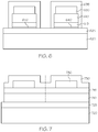
- the flexible support 610 has a pre-applied barrier stack 615 .
- the flexible support 610 is cut into discrete sheets sized for the environmentally sensitive device 630 .
- the flexible substrate 610 with the barrier stack 615 is temporarily laminated to the rigid support 620 using a reversible adhesive 625 .
- the individual layers of the barrier stacks are not shown.
- the barrier stack 615 faces the adhesive 625 , rather than the flexible substrate 610 facing the adhesive 625 .
- An optional functional layer 640 such as a scratch resistant layer, can be included over the barrier stack 615 and would serve as the interface between the barrier stack 615 and the adhesive 625 .
- the environmentally sensitive device 630 is fabricated adjacent to the flexible support 610 , and is encapsulated by the second barrier stack 635 , which has an edge seal. This arrangement allows the second barrier stack 635 to protect the edges of the first barrier stack 615 which were exposed when the flexible substrate 610 and first barrier stack 615 were cut into discrete sheets.
- the second barrier could be a sheet of a barrier material, such as a sheet of a metal or metal foil, which can be laminated over the environmentally sensitive device.
- FIG. 7 shows another method of making encapsulated environmentally sensitive devices.
- the flexible substrate 710 includes a pre-applied three dimensional barrier 745 .
- the flexible substrate 710 is temporarily laminated to the rigid support 720 using a reversible adhesive 725 .
- the environmentally sensitive device 730 is fabricated adjacent to the flexible support 710 .
- a second three dimensional barrier 750 encapsulates the environmentally sensitive device 730 .
- the adhesive 725 can be reversed, and the rigid support 720 removed.
- the flexible substrate 710 can be cut to separate the individual encapsulated environmentally sensitive devices.
- One advantage of the three dimensional first and second barriers is that cutting the barriers does not compromise the barrier.
- a method of making a three dimensional barrier is described in U.S. application Ser. No. 11/627,583, filed concurrently herewith, entitled “Three Dimensional Multilayer Barrier and Method of Making”, which is incorporated by reference herein. Another method is shown in FIG. 8 .
- the flexible substrate could be a metal or metal foil.
- the flexible substrate 810 is temporarily laminated to the rigid support 820 using reversible adhesive 825 .
- a second barrier stack 835 is applied adjacent to the environmentally sensitive device 830 .
- the second barrier stack 835 can be applied by laminating a flexible film 840 with a pre-applied second barrier 835 using an adhesive 845 .
- Other methods of lamination could be used including, but not limited to, using heat.
- a gettering material could be included between the adhesive 845 and the environmentally sensitive device 830 .
- a cover sheet could be laminated to an array of environmentally sensitive devices.
- the adhesive/sealant (and optional getter) could be patterned to surround each of the array of devices on the flexible substrate using a mask or a printing technique such as ink jet.
- Another method is the use of a layer of adhesive/sealant applied to the entire surface (the devices as well as the area between devices).
- a third method is to use pick and place equipment to apply individual covers to each of the devices. In this case, the adhesive/sealant could be applied as described in either of the first two approaches.
- the second barrier 835 could be deposited adjacent to the environmentally sensitive device 830 using vacuum or atmospheric processes. In this case, the flexible film 840 and adhesive 845 would not be used.
- the barrier stacks can include at least one decoupling layer and at least one barrier layer.
- a suitable arrangement for the encapsulated environmentally sensitive device is shown in FIG. 9 .
- the flexible substrate 910 is temporarily laminated to the rigid support 920 using a reversible adhesive 925 .
- First barrier stacks 915 are adjacent to the flexible substrate 910 .
- the environmentally sensitive device 930 is adjacent to the first barrier stacks 915 .
- the second barrier stacks 935 are adjacent to the environmentally sensitive device 930 .
- the first and second barrier stacks 915 , 935 are made of alternating decoupling layers 940 and barrier layers 945 .
- first barrier stacks 915 There are five first barrier stacks 915 of alternating decoupling layers and barrier layers, and seven second barrier stacks 935 .
- the barrier layer adjacent to the environmentally sensitive device can be thicker than the other barrier layers, and the last decoupling layer (the top layer) can be thicker than the other decoupling layers, if desired.
- FIG. 9 shows only the order of the various layers; it does not show the edge seals for the barrier stacks.
- FIG. 10 shows one embodiment of a structure which was tested.
- the flexible substrate 1005 was polyethylene naphthenate. It had a hard coat layer (SDC Technology, crystal coat MP 101) 1010 on both sides. It also had pre-applied barrier stacks 1015 containing 5 sets of alternating layers of aluminum oxide 1020 and acrylate polymer 1025 and an additional aluminum oxide layer 1020 .
- the flexible substrate and barrier stacks were temporarily laminated to the rigid glass support 1030 using a reversible adhesive (3M 668 Thermo Bond) 1035 .
- a layer of calcium 1040 which is used to test barrier performance, was then deposited over the first barrier stacks 1015 .
- the calcium test is described in Nisato et al., “Thin Film Encapsulation for OLEDs: Evaluation of Multi-layer Barriers using the Ca Test,” SID 03 Digest, 2003, p. 550-553, which is incorporated herein by reference.
- the second barrier stacks 1045 were then deposited.
- the second barrier stacks were 7 sets of alternating layers of aluminum oxide 1050 and acrylate polymer 1055 .
- the first oxide layer (adjacent to the layer of calcium 1040 ) and the last polymer layer (the top layer) were thicker than the remaining layers. These samples had rather short lifetimes, typically about 25 hours at 60° C. and 90% RH. The best results were about 100 hours, but there was significant damage to the barrier coated flexible substrate.
- the experiment was repeated by laminating the flexible substrate with the pre-applied barrier stacks to the rigid glass support. Three layers, a fast process aluminum oxide, acrylate polymer, and aluminum oxide were deposited on the barrier stacks prior to deposition and encapsulation of the Ca test patch. This was done to solve issues which were believed to be due to debris from shipping and/or handling of the flexible substrate and barrier stacks. This experiment showed excellent results, with about 90% of the Ca samples passing after 500 hours at 60° C. and 90% RH.
Abstract
Methods of encapsulating an environmentally sensitive device. The methods involve temporarily laminating a flexible substrate to a rigid support using a reversible adhesive for processing, reversing the reversible adhesive, and removing the device from the rigid support.
Description
This application is a continuation of U.S. patent application Ser. No. 14/669,216, filed Mar. 26, 2015, now allowed, which is a divisional of U.S. patent application Ser. No. 11/627,602, filed Jan. 26, 2007, now abandoned. This application is related to U.S. application Ser. No. 11/068,356, filed Feb. 28, 2005, which is a divisional of U.S. application Ser. No. 09/966,163, filed Sep. 28, 2001, now U.S. Pat. No. 6,866,901, which is a continuation-in-part of U.S. application Ser. No. 09/427,138, filed Oct. 25, 1999, now U.S. Pat. No. 6,522,067.
Many devices are subject to degradation caused by permeation of environmental gases or liquids, such as oxygen and water vapor in the atmosphere or chemicals used in the processing of the electronic product. The devices are usually encapsulated in order to prevent degradation.
Various types of encapsulated devices are known. For example, U.S. Pat. No. 6,268,695, entitled “Environmental Barrier Material For Organic Light Emitting Device And Method Of Making,” issued Jul. 31, 2001; U.S. Pat. No. 6,522,067, entitled “Environmental Barrier Material For Organic Light Emitting Device And Method Of Making,” issued Feb. 18, 2003; and U.S. Pat. No. 6,570,325, entitled “Environmental Barrier Material For Organic Light Emitting Device And Method Of Making”, issued May 27, 2003, all of which are incorporated herein by reference, describe encapsulated organic light emitting devices (OLEDs). U.S. Pat. No. 6,573,652, entitled “Encapsulated Display Devices”, issued Jun. 3, 2003, which is incorporated herein by reference, describes encapsulated liquid crystal displays (LCDs), light emitting diodes (LEDs), light emitting polymers (LEPs), electronic signage using electrophoretic inks, electroluminescent devices (EDs), and phosphorescent devices. U.S. Pat. No. 6,548,912, entitled “Semiconductor Passivation Using Barrier Coatings,” issued Apr. 15, 2003, which is incorporated herein by reference, describes encapsulated microelectronic devices, including integrated circuits, charge coupled devices, light emitting diodes, light emitting polymers, organic light emitting devices, metal sensor pads, micro-disk lasers, electrochromic devices, photochromic devices, microelectromechanical systems, and solar cells.
Generally, encapsulated devices can be made by depositing barrier stacks adjacent to one or both sides of the device. The barrier stacks typically include at least one barrier layer and at least one decoupling layer. There could be one decoupling layer and one barrier layer, there could be multiple decoupling layers on one side of one or more barrier layers, or there could be one or more decoupling layers on both sides of one or more barrier layers. The important feature is that the barrier stack has at least one decoupling layer and at least one barrier layer.
One embodiment of an encapsulated display device is shown in FIG. 1 . The encapsulated display device 100 includes a substrate 105, a display device 110, and a barrier stack 115. The barrier stack 115 includes a barrier layer 120 and a decoupling layer 125. The barrier stack 115 encapsulates the display device 110, preventing environmental oxygen and water vapor from degrading the display device.
The barrier layers and decoupling layers in the barrier stack can be made of the same material or of a different material. The barrier layers are typically about 100-1000 Å thick, and the decoupling layers are typically about 1000-10,000 Å thick.
Although only one barrier stack is shown in FIG. 1 , the number of barrier stacks is not limited. The number of barrier stacks needed depends on the level of water vapor and oxygen permeation resistance needed for the particular application. One or two barrier stacks should provide sufficient barrier properties for many applications, and three or four barrier stacks should be sufficient for most. The most stringent applications may require five or more barrier stacks.
The barrier layers can be deposited using a vacuum process, such as sputtering, chemical vapor deposition, plasma enhanced chemical vapor deposition, evaporation, sublimation, electron cyclotron resonance-plasma enhanced vapor deposition (ECR-PECVD), and combinations thereof. Suitable barrier materials include, but are not limited to, metals, metal oxides, metal nitrides, metal carbides, metal oxynitrides, metal oxyborides, and combinations thereof. The barrier layers can be graded composition barriers, if desired. Suitable graded composition barriers include, but are not limited to, those described in U.S. Pat. No. 7,015,640, which is incorporated herein by reference.
The decoupling layers can be deposited using vacuum processes, such as flash evaporation with in situ polymerization under vacuum, or plasma deposition and polymerization, or atmospheric processes, such as spin coating, ink jet printing, screen printing, or spraying. Suitable materials for the decoupling layer, include, but are not limited to, organic polymers, inorganic polymers, organometallic polymers, hybrid organic/inorganic polymer systems, and silicates.
Handling flexible substrates as discrete sheets during the encapsulation of environmentally sensitive devices is difficult. The discrete sheets must be positioned correctly in relationship to the various pieces of equipment for depositing barriers, devices, etc. For example, many of the deposition steps utilize masks which must be positioned accurately and reproducibly with respect to the substrate to obtain the proper coverage. In order to maintain the correct position during processing, the discrete sheets need to rest on a rigid substrate or be held tightly by a clamping system. However, it is not easy to retain a polymeric sheet by mechanical clamping because of the plastic nature (e.g., flow and distortion under applied stress) of a flexible substrate. Furthermore, the encapsulation process imparts heat to a polymeric substrate, which has two adverse effects. Plastic flow leading to distortion increases significantly with heating of the film and may become catastrophic when the Tg is reached. Although the coefficient of thermal expansion (TCE) may not seem important, it is significant in an x-y plane when the dimensions are several inches by several inches. Both effects can cause a sheet of film which is initially tightly held at a temperature at the onset of processing to relax and distort as processing heats the film. In addition, another common system cannot be used with vacuum deposition processes. In that arrangement, the film is positioned on a rigid plate that has channels connected to a vacuum system, and a vacuum pump is used to establish a vacuum under the film at the contact of the film with the plate that holds the film in place. The film is held by the atmospheric pressure on the exposed surface of the film. However, this cannot be done in a vacuum environment.
In addition, the use of barriers on flexible substrates in roll form presents a significant issue. No matter how they are used as substrates for devices, the operation of cutting the substrate to an appropriate size for the finished device exposes the cut edges to the permeation of contaminants. The proposed solutions for this problem generally require additional, precision manufacturing steps, or result in a construction that sacrifices some or all of the advantages of the flexible substrate.
Therefore, there is a need for a method of handling discrete sheets during encapsulation of environmentally sensitive devices.
The present invention meets this need by providing a method of encapsulating an environmentally sensitive device. The method comprises providing a flexible substrate; cutting the flexible substrate into a discrete sheet; temporarily laminating the flexible substrate to a rigid support using a reversible adhesive; optionally applying a first barrier stack adjacent to the flexible substrate, the first barrier stack comprising at least one barrier layer and at least one decoupling layer; applying the environmentally sensitive device adjacent to the flexible substrate; applying a second barrier stack adjacent to the environmentally sensitive device, the second barrier stack comprising at least one barrier layer and at least one decoupling layer, the environmentally sensitive device being encapsulated between the substrate and the second barrier stack, the substrate and the second barrier stack forming a seal, or between the first barrier stack and the second barrier stack, the first and second barrier stacks forming a seal; and reversing the reversible adhesive and removing the encapsulated environmentally sensitive device from the rigid support.
In another embodiment, the method comprises providing a flexible substrate in discrete sheet form; temporarily laminating the flexible substrate adjacent to a rigid support; applying a first barrier stack adjacent to the flexible substrate, the first barrier stack comprising at least one barrier layer and at least one decoupling layer; applying the environmentally sensitive device adjacent to the flexible substrate; applying a sheet of barrier material adjacent to the environmentally sensitive device to encapsulate the environmentally sensitive device between the first barrier stack and the sheet of barrier material, the first barrier stack and the sheet of barrier material forming a seal; and removing the encapsulated environmentally sensitive device from the rigid support.
By adjacent to, we mean next to, but not necessarily directly next to. There can be additional layers between two adjacent layers.
The present invention uses an easily reversible lamination to hold discrete sheets of the flexible substrate on the rigid support. This provides a construction which is more compatible with current fabrication processes and equipment for environmentally sensitive devices such as OLEDs. The temperature uniformity is as good as that for glass, which allows a uniform deposition of the monomer on the discrete sheet of flexible substrate. The invention also includes a solvent-free debonding process, avoiding the complications associated with the use of solvents.
One advantage of supporting flexible substrates on a rigid support is that the sheet of flexible substrate is positioned once on the rigid support and held by an adhesive which is effective in a vacuum environment. Clamping systems developed for rigid materials, such as glass coating technologies, silicon wafer technologies, printed circuit board technologies, chips, etc, processed in vacuum environments can be used. Precise placement means can also be used. Bonding the flexible film to a rigid support provides superior heat transfer between the film and the support, allowing the support to be a more effective heat sink for unwanted process heating. Although the flexible film still has a TCE, careful selection of the adhesives and rigid supports can level the differences and so the potential expansion related issues. In addition, the adhesive is a plastic by nature (i.e., it can flow and distort when heated) and can take up thermal expansions.
Generally, the process of the present invention includes providing a flexible substrate; cutting the flexible substrate into a discrete sheet; temporarily laminating the flexible substrate to a rigid support using a reversible adhesive; optionally applying a first barrier stack adjacent to the flexible substrate, the first barrier stack comprising at least one barrier layer and at least one decoupling layer; applying the environmentally sensitive device adjacent to the flexible substrate; applying a second barrier stack adjacent to the environmentally sensitive device, the second barrier stack comprising at least one barrier layer and at least one decoupling layer, the environmentally sensitive device being encapsulated between the substrate and the second barrier stack, the substrate and the second barrier stack forming a seal, or between the first barrier stack and the second barrier stack, the first and second barrier stacks forming a seal; and reversing the reversible adhesive and removing the encapsulated environmentally sensitive device from the rigid support.
Suitable flexible substrates include, but are not limited to, polymer films, metals, and metal foils.
The flexible substrate can include one or more functional layers. Suitable functional layers include, but are not limited to, planarizing layers, adhesion promoting layers, scratch resistant layers, organic or inorganic layers, anti-reflective coatings, anti-fingerprint coatings, anti-static coatings, electrically conductive layers, electrode layers, and combinations thereof.
The flexible substrate can include a first barrier stack, or a first barrier stack can be added during processing. The first barrier stack can be applied using a variety of approaches, including but not limited to, processes which create an edge seal. Suitable edge sealing processes are described in U.S. Pat. No. 6,866,901, which is incorporated herein by reference.
Where a discrete sheet is to carry an array of devices, the first barrier stack can be created as an array of appropriately dimensioned regions with sealed edges. Although the masking of such an array provides a significant challenge, it is viable given the established masking capability currently in existence.
Environmentally sensitive devices include, but are not limited to, organic light emitting devices, liquid crystal displays, displays using electrophoretic inks, light emitting diodes, light emitting polymers, electroluminescent devices, phosphorescent devices, electrophoretic inks, organic solar cells, inorganic solar cells, thin film batteries, thin film devices with vias, integrated circuits, charge coupled devices, metal sensor pads, micro-disk lasers, electrochromic devices, photochromic devices, microelectromechanical systems, and solar cells, and combinations thereof.
The environmentally sensitive device is sealed between the substrate and the second barrier stack, or between a first barrier stack and a second barrier stack, which encapsulate the environmentally sensitive device. The second barrier stack can be applied using various processes which form an edge seal.
Heat activated adhesives are heated to activate the adhesive and to reverse it. Suitable heat activated adhesives include, but are not limited to, polyamides, ethylene-vinyl alcohol copolymers, ethylene-vinyl acetate copolymers, hydrocarbon resins, acrylics, and acrylic copolymers. The heat activated adhesives can include additional components which can modify the properties, including control of activation temperature, tack, melt viscosity, thermal stability, and adhesion to specific substrates. The additional components can desirably be selected so that the adhesive is free of components that will become migratory in a vacuum environment. The adhesive is desirably applied under conditions that do not entrain excessive air.
Pressure sensitive adhesives are based on controlling the strength of adhesion so that the pressure sensitive adhesives can adhere a first substrate upon which they are emplaced to a surface of a second substrate via contact under pressure, but with limited strength of adhesion so that they will allow the first substrate to be removed from the second substrate when the removal force exceeds the adhesive strength. When properly formulated, they have significantly higher adhesion to the first substrate so that they remain anchored to the first substrate when it is removed. The pressure sensitive adhesive could be applied to the rigid support, which would allow the removal of the encapsulated device on a flexible substrate without the need to clean an adhesive layer from the flexible substrate. For example, a supply of rigid supports could be prepared with a pre-applied pressure sensitive adhesive and a release sheet to prevent debris from attaching to the adhesive surface. These rigid supports could be fed to a flexible substrate alignment and attachment station. A supply of pre-cut flexible film substrates, either with or without a device, could be fed to the alignment and attachment station, positioned, and contacted to make the laminate. This type of pick and place station and process is used for placing chips onto boards.
UV activated adhesives provide an adhesive surface as applied. This allows the flexible substrate to be adhered to the rigid support. UV exposure results in loss of adhesion and therefore, release of the flexible substrate. Differing mechanisms can provide this result. One is to incorporate a component into the coating formulation that degrades in response to UV exposure thereby reducing and/or eliminating the adhesive properties of the coating. The other is to include a component in the coating that undergoes considerable cross-linking (polymerization) in response to UV exposure. Cross-linking and shrinkage accompanying cross-linking often result in a reduction in adhesion when the mechanisms involved do not include reacting with the surfaces in contact with the cross-linked coating. When initially applied, the coating has adhesive properties, but when exposed to UV radiation, cross-linking occurs, resulting in a loss of adhesive properties.
Another consideration is application method. One common approach involves heating the adhesive to form a melt that can be coated and “frozen” in place. An alternative is to dissolve the adhesive composition in a solvent and apply the mixture using conventional atmospheric coating processes. This process has the advantage of a superior ability to control the amount and uniformity of the adhesive deposited. It is also possible using conventional coating processes to apply adhesives as a blend of precursors that are reacted (partially cross-linked) after application to form an adhesive layer. Pressure sensitive acrylic and urethane based adhesives are commonly applied using this approach. Blends of reactive precursors can be essentially 100% solids. If the components are selected with low vapor pressures, they could be applied in a vacuum, if desired. Alternatively, they can be combined with a solvent for ease of application, and the solvent can be removed by evaporation after application and prior to initiation of the cure. The latter approach typically uses oligomeric components that are self-crosslinking to avoid issues with azeotropes formed between low molecular weight precursors and the solvent(s) used for coating.
Another consideration is the surface to be coated with the reversible adhesive. It is significantly easier to coat a web than a discrete sheet. However, handling barrier coated films requires particular care to avoid damage, accumulated debris, or premature exposure to environmental contaminants. Therefore, it may be desirable to apply the adhesive to the rigid support, helping to minimize handling of the barrier coated film.
The environmentally sensitive devices 230 are then applied adjacent to the first barrier stack 215 on the flexible substrate 210. The environmentally sensitive device can be applied by direct deposition, or it can be fabricated first and then placed adjacent to the first barrier stack.
A second barrier stack 235, which includes an edge seal, is applied adjacent to the environmentally sensitive devices 230, which are sealed between the first barrier stack 215 and the second barrier stack 235.
After the environmentally sensitive devices 230 are encapsulated, the adhesive 225 is reversed using a method appropriate to the type of reversible adhesive.
The individual encapsulated environmentally sensitive devices can be separated by cutting the flexible support 210 and first barrier stack 215. However, cutting through the first barrier stack can expose the various layers of the first barrier stack to contaminants.
Another method of making encapsulated environmentally sensitive devices is shown in FIG. 3 . In this case, the flexible substrate 310 is temporarily laminated to the rigid support 320 using a reversible adhesive 325. The first barrier stack 315, which includes an edge seal, is applied after the flexible substrate 310 has been laminated adjacent to the rigid support 320. The individual layers of the barrier stacks are not shown. The first barrier stack 315 is applied over discrete areas of the flexible support 310, using masks, for example. The environmentally sensitive device 330 is encapsulated by the second barrier stack 335, which has an edge seal. The adhesive 325 can be reversed, and the rigid support 320 removed.
The individual encapsulated environmentally sensitive devices can be separated by cutting through the flexible substrate 310. In this embodiment, because the first barrier stack 315 was applied over discrete areas of the flexible substrate 310, the individual encapsulated environmentally sensitive devices can be separated without cutting through the first barrier stack 315. This avoids the damage that is often noted when barrier stack assemblies are cut.
The adhesive layer 425 can be replaced after each cycle, if desired. This helps to eliminate problems with contaminants and debris becoming trapped in the adhesive.
Another method is shown in FIG. 5 . In this arrangement, the flexible support 510 is cut into discrete sheets having an appropriate size for environmentally sensitive device 530. The discrete sheets of the flexible substrate 510 are temporarily laminated to the rigid support 520 with the reversible adhesive 525. The first barrier stack 515, which has an edge seal, is deposited adjacent to the flexible substrate 510. The individual layers of the barrier stacks are not shown. The environmentally sensitive device 530 is fabricated adjacent to the first barrier stack 515, and the second barrier stack 535, which has an edge seal, encapsulates it. The adhesive 525 is reversed, and the rigid support 520 removed. The removal of the rigid support 520 separates the individual encapsulated environmentally sensitive devices; no cutting is necessary.
Still another method is shown in FIG. 6 . The flexible support 610 has a pre-applied barrier stack 615. The flexible support 610 is cut into discrete sheets sized for the environmentally sensitive device 630. The flexible substrate 610 with the barrier stack 615 is temporarily laminated to the rigid support 620 using a reversible adhesive 625. The individual layers of the barrier stacks are not shown. In this arrangement, the barrier stack 615 faces the adhesive 625, rather than the flexible substrate 610 facing the adhesive 625. An optional functional layer 640, such as a scratch resistant layer, can be included over the barrier stack 615 and would serve as the interface between the barrier stack 615 and the adhesive 625. The environmentally sensitive device 630 is fabricated adjacent to the flexible support 610, and is encapsulated by the second barrier stack 635, which has an edge seal. This arrangement allows the second barrier stack 635 to protect the edges of the first barrier stack 615 which were exposed when the flexible substrate 610 and first barrier stack 615 were cut into discrete sheets.
Alternatively in FIGS. 2-6 , the second barrier could be a sheet of a barrier material, such as a sheet of a metal or metal foil, which can be laminated over the environmentally sensitive device. FIG. 7 shows another method of making encapsulated environmentally sensitive devices. In this arrangement, the flexible substrate 710 includes a pre-applied three dimensional barrier 745. The flexible substrate 710 is temporarily laminated to the rigid support 720 using a reversible adhesive 725. The environmentally sensitive device 730 is fabricated adjacent to the flexible support 710. A second three dimensional barrier 750 encapsulates the environmentally sensitive device 730. The adhesive 725 can be reversed, and the rigid support 720 removed. The flexible substrate 710 can be cut to separate the individual encapsulated environmentally sensitive devices. One advantage of the three dimensional first and second barriers is that cutting the barriers does not compromise the barrier. A method of making a three dimensional barrier is described in U.S. application Ser. No. 11/627,583, filed concurrently herewith, entitled “Three Dimensional Multilayer Barrier and Method of Making”, which is incorporated by reference herein. Another method is shown in FIG. 8 . In this embodiment, there is no barrier stack on the flexible substrate 810. For example, the flexible substrate could be a metal or metal foil. The flexible substrate 810 is temporarily laminated to the rigid support 820 using reversible adhesive 825. A second barrier stack 835 is applied adjacent to the environmentally sensitive device 830. The second barrier stack 835 can be applied by laminating a flexible film 840 with a pre-applied second barrier 835 using an adhesive 845. Other methods of lamination could be used including, but not limited to, using heat. A gettering material could be included between the adhesive 845 and the environmentally sensitive device 830.
A cover sheet could be laminated to an array of environmentally sensitive devices. The adhesive/sealant (and optional getter) could be patterned to surround each of the array of devices on the flexible substrate using a mask or a printing technique such as ink jet. Another method is the use of a layer of adhesive/sealant applied to the entire surface (the devices as well as the area between devices). A third method is to use pick and place equipment to apply individual covers to each of the devices. In this case, the adhesive/sealant could be applied as described in either of the first two approaches.
Alternatively, the second barrier 835 could be deposited adjacent to the environmentally sensitive device 830 using vacuum or atmospheric processes. In this case, the flexible film 840 and adhesive 845 would not be used.
There can be one or more first and/or second barrier stacks. The barrier stacks can include at least one decoupling layer and at least one barrier layer. For example, a suitable arrangement for the encapsulated environmentally sensitive device is shown in FIG. 9 . The flexible substrate 910 is temporarily laminated to the rigid support 920 using a reversible adhesive 925. First barrier stacks 915 are adjacent to the flexible substrate 910. The environmentally sensitive device 930 is adjacent to the first barrier stacks 915. The second barrier stacks 935 are adjacent to the environmentally sensitive device 930. The first and second barrier stacks 915, 935 are made of alternating decoupling layers 940 and barrier layers 945. There are five first barrier stacks 915 of alternating decoupling layers and barrier layers, and seven second barrier stacks 935. In the second barrier stacks 935, the barrier layer adjacent to the environmentally sensitive device can be thicker than the other barrier layers, and the last decoupling layer (the top layer) can be thicker than the other decoupling layers, if desired. FIG. 9 shows only the order of the various layers; it does not show the edge seals for the barrier stacks.
The experiment was repeated by laminating the flexible substrate with the pre-applied barrier stacks to the rigid glass support. Three layers, a fast process aluminum oxide, acrylate polymer, and aluminum oxide were deposited on the barrier stacks prior to deposition and encapsulation of the Ca test patch. This was done to solve issues which were believed to be due to debris from shipping and/or handling of the flexible substrate and barrier stacks. This experiment showed excellent results, with about 90% of the Ca samples passing after 500 hours at 60° C. and 90% RH.
While certain representative embodiments and details have been shown for purposes of illustrating the invention, it will be apparent to those skilled in the art that various changes in the compositions and methods disclosed herein may be made without departing from the scope of the invention, which is defined in the appended claims.
Claims (11)
1. A method of encapsulating environmentally sensitive devices, the method comprising:
providing a flexible substrate;
temporarily laminating the flexible substrate adjacent to a rigid support with a reversible adhesive;
masking regions on the flexible substrate to define areas corresponding to first barrier stacks;
applying the first barrier stacks adjacent to the flexible substrate after the flexible substrate is laminated adjacent to the rigid support, each of the first barrier stacks comprising at least one barrier layer and at least one decoupling layer;
applying the environmentally sensitive devices over the flexible substrate such that the environmentally sensitive devices are formed adjacent to the first barrier stacks;
applying second barrier stacks adjacent to the environmentally sensitive devices, each of the second barrier stacks comprising at least one barrier layer and at least one decoupling layer such that an edge seal is formed by each of the second barrier stacks about each of the edges of the environmentally sensitive devices, each of the environmentally sensitive devices being encapsulated between a corresponding first barrier stack and a corresponding second barrier stack;
removing the flexible substrate from the rigid support by decoupling the adhesive; and
cutting the flexible substrate between the defined areas after such removing.
2. The method of claim 1 wherein the flexible substrate is cut into discrete sheet form after the flexible substrate is laminated adjacent to the rigid support.
3. The method of claim 1 wherein the flexible substrate is cut into discrete sheet form and wherein the first barrier stacks are applied before the flexible substrate is cut into the discrete sheet form.
4. The method of claim 1 wherein the first barrier stacks are applied using a mask.
5. The method of claim 1 wherein the second barrier stacks are applied using a mask.
6. The method of claim 1 further comprising applying a functional layer adjacent to the flexible substrate.
7. The method of claim 1 wherein applying a second barrier stacks adjacent to the environmentally sensitive devices comprises depositing the second barrier stacks adjacent to the environmentally sensitive devices.
8. The method of claim 7 wherein depositing the second barrier stacks adjacent to the environmentally sensitive devices comprises vacuum depositing the second barrier stacks adjacent to the environmentally sensitive devices.
9. The method of claim 7 wherein the second barrier stacks are laminated adjacent to the environmentally sensitive devices using heat, adhesive, or combinations thereof.
10. The method of claim 1 wherein applying second barrier stacks adjacent to the environmentally sensitive devices comprises laminating the second barrier stacks adjacent to the environmentally sensitive devices.
11. The method of claim 1 further comprising applying an array of thin film transistors before the environmentally sensitive devices are applied.
Priority Applications (1)
| Application Number | Priority Date | Filing Date | Title |
|---|---|---|---|
| US16/717,261 US10950821B2 (en) | 2007-01-26 | 2019-12-17 | Method of encapsulating an environmentally sensitive device |
Applications Claiming Priority (3)
| Application Number | Priority Date | Filing Date | Title |
|---|---|---|---|
| US11/627,602 US20100330748A1 (en) | 1999-10-25 | 2007-01-26 | Method of encapsulating an environmentally sensitive device |
| US14/669,216 US20150191000A1 (en) | 1999-10-25 | 2015-03-26 | Method of encapsulating an environmentally sensitive device |
| US16/717,261 US10950821B2 (en) | 2007-01-26 | 2019-12-17 | Method of encapsulating an environmentally sensitive device |
Related Parent Applications (1)
| Application Number | Title | Priority Date | Filing Date |
|---|---|---|---|
| US14/669,216 Continuation US20150191000A1 (en) | 1999-10-25 | 2015-03-26 | Method of encapsulating an environmentally sensitive device |
Publications (2)
| Publication Number | Publication Date |
|---|---|
| US20200119309A1 US20200119309A1 (en) | 2020-04-16 |
| US10950821B2 true US10950821B2 (en) | 2021-03-16 |
Family
ID=39183021
Family Applications (3)
| Application Number | Title | Priority Date | Filing Date |
|---|---|---|---|
| US11/627,602 Abandoned US20100330748A1 (en) | 1999-10-25 | 2007-01-26 | Method of encapsulating an environmentally sensitive device |
| US14/669,216 Abandoned US20150191000A1 (en) | 1999-10-25 | 2015-03-26 | Method of encapsulating an environmentally sensitive device |
| US16/717,261 Active US10950821B2 (en) | 2007-01-26 | 2019-12-17 | Method of encapsulating an environmentally sensitive device |
Family Applications Before (2)
| Application Number | Title | Priority Date | Filing Date |
|---|---|---|---|
| US11/627,602 Abandoned US20100330748A1 (en) | 1999-10-25 | 2007-01-26 | Method of encapsulating an environmentally sensitive device |
| US14/669,216 Abandoned US20150191000A1 (en) | 1999-10-25 | 2015-03-26 | Method of encapsulating an environmentally sensitive device |
Country Status (5)
| Country | Link |
|---|---|
| US (3) | US20100330748A1 (en) |
| EP (1) | EP2126999A1 (en) |
| JP (1) | JP5511388B2 (en) |
| TW (1) | TWI404248B (en) |
| WO (1) | WO2008094353A1 (en) |
Cited By (1)
| Publication number | Priority date | Publication date | Assignee | Title |
|---|---|---|---|---|
| US11019721B2 (en) * | 2019-09-05 | 2021-05-25 | Hannstouch Solution Incorporated | Manufacturing method of flexible electronic device |
Families Citing this family (24)
| Publication number | Priority date | Publication date | Assignee | Title |
|---|---|---|---|---|
| WO2009155084A1 (en) * | 2008-05-30 | 2009-12-23 | Stryker Corporation | Method of assembling an electrode array that includes a plastically deformable carrier |
| US9991311B2 (en) | 2008-12-02 | 2018-06-05 | Arizona Board Of Regents On Behalf Of Arizona State University | Dual active layer semiconductor device and method of manufacturing the same |
| US9601530B2 (en) | 2008-12-02 | 2017-03-21 | Arizona Board Of Regents, A Body Corporated Of The State Of Arizona, Acting For And On Behalf Of Arizona State University | Dual active layer semiconductor device and method of manufacturing the same |
| US9721825B2 (en) | 2008-12-02 | 2017-08-01 | Arizona Board Of Regents, A Body Corporate Of The State Of Arizona, Acting For And On Behalf Of Arizona State University | Method of providing a flexible semiconductor device and flexible semiconductor device thereof |
| KR101362025B1 (en) | 2009-05-29 | 2014-02-13 | 아리조나 보드 오브 리젠츠 퍼 앤 온 비하프 오브 아리조나 스테이트 유니버시티 | Method of providing a flexible semiconductor device at high temperatures and flexible semiconductor device thereof |
| FR2949776B1 (en) | 2009-09-10 | 2013-05-17 | Saint Gobain Performance Plast | LAYERED ELEMENT FOR ENCAPSULATING A SENSITIVE ELEMENT |
| FR2949775B1 (en) | 2009-09-10 | 2013-08-09 | Saint Gobain Performance Plast | PROTECTIVE SUBSTRATE FOR COLOR DEVICE OR RADIATION TRANSMITTER |
| WO2012021196A2 (en) * | 2010-05-21 | 2012-02-16 | Arizona Board Of Regents, For And On Behalf Of Arizona State University | Method for manufacturing electronic devices and electronic devices thereof |
| WO2012021197A2 (en) * | 2010-05-21 | 2012-02-16 | Arizona Board Of Regents, For And On Behalf Of Arizona State University | Method of manufacturing electronic devices on both sides of a carrier substrate and electronic devices thereof |
| GB2481367B (en) * | 2010-06-04 | 2015-01-14 | Plastic Logic Ltd | Moisture Barrier for Electronic Devices |
| FR2973939A1 (en) * | 2011-04-08 | 2012-10-12 | Saint Gobain | LAYERED ELEMENT FOR ENCAPSULATING A SENSITIVE ELEMENT |
| KR101971202B1 (en) * | 2012-11-22 | 2019-04-23 | 삼성디스플레이 주식회사 | Organic light emitting display apparatus and the manufacturing method thereof |
| WO2017034645A2 (en) | 2015-06-09 | 2017-03-02 | ARIZONA BOARD OF REGENTS, a body corporate for THE STATE OF ARIZONA for and on behalf of ARIZONA STATE UNIVERSITY | Method of providing an electronic device and electronic device thereof |
| WO2015175353A1 (en) | 2014-05-13 | 2015-11-19 | Arizona Board Of Regents, For And On Behalf Of Arizona State University | Method of providing an electronic device and electronic device thereof |
| US10381224B2 (en) | 2014-01-23 | 2019-08-13 | Arizona Board Of Regents On Behalf Of Arizona State University | Method of providing an electronic device and electronic device thereof |
| WO2015156891A2 (en) | 2014-01-23 | 2015-10-15 | Arizona Board Of Regents, Acting For And On Behalf Of Arizona State University | Method of providing a flexible semiconductor device and flexible semiconductor device thereof |
| JP6374188B2 (en) * | 2014-03-14 | 2018-08-15 | 東京エレクトロン株式会社 | Method for forming sealing structure, manufacturing apparatus for sealing structure, manufacturing method for organic EL element structure, and manufacturing apparatus therefor |
| JP6946185B2 (en) * | 2014-11-17 | 2021-10-06 | セイジ・エレクトロクロミクス,インコーポレイテッド | Multiple barrier layer sealed laminate |
| US10446582B2 (en) | 2014-12-22 | 2019-10-15 | Arizona Board Of Regents On Behalf Of Arizona State University | Method of providing an imaging system and imaging system thereof |
| US9741742B2 (en) | 2014-12-22 | 2017-08-22 | Arizona Board Of Regents, A Body Corporate Of The State Of Arizona, Acting For And On Behalf Of Arizona State University | Deformable electronic device and methods of providing and using deformable electronic device |
| WO2016132460A1 (en) | 2015-02-17 | 2016-08-25 | パイオニア株式会社 | Light-emitting device |
| KR102486876B1 (en) * | 2015-07-07 | 2023-01-11 | 삼성디스플레이 주식회사 | Organic light-emitting display apparatus and manufacturing the same |
| CN108417737A (en) * | 2018-03-07 | 2018-08-17 | 京东方科技集团股份有限公司 | Production method, display panel and the display device of display panel |
| JP2019117808A (en) * | 2019-04-24 | 2019-07-18 | パイオニア株式会社 | Light-emitting device |
Citations (393)
| Publication number | Priority date | Publication date | Assignee | Title |
|---|---|---|---|---|
| US2382432A (en) | 1940-08-02 | 1945-08-14 | Crown Cork & Seal Co | Method and apparatus for depositing vaporized metal coatings |
| US2384500A (en) | 1942-07-08 | 1945-09-11 | Crown Cork & Seal Co | Apparatus and method of coating |
| JPS414440Y1 (en) | 1964-04-20 | 1966-03-15 | ||
| BE704297A (en) | 1965-09-13 | 1968-02-01 | ||
| JPS448515Y1 (en) | 1966-07-27 | 1969-04-04 | ||
| US3475307A (en) | 1965-02-04 | 1969-10-28 | Continental Can Co | Condensation of monomer vapors to increase polymerization rates in a glow discharge |
| US3496427A (en) | 1966-01-13 | 1970-02-17 | Gen Electric | Semiconductor device with composite encapsulation |
| US3607365A (en) | 1969-05-12 | 1971-09-21 | Minnesota Mining & Mfg | Vapor phase method of coating substrates with polymeric coating |
| US3661117A (en) | 1969-12-03 | 1972-05-09 | Stanford Research Inst | Apparatus for depositing thin lines |
| US3941630A (en) | 1974-04-29 | 1976-03-02 | Rca Corporation | Method of fabricating a charged couple radiation sensing device |
| JPS5147678A (en) | 1974-10-22 | 1976-04-23 | Ts Pk B Kuzunechino Puresusobo | SENZAIYOJIDOEN SHINSETSUDANKIKAINO MAIKATSUTAA |
| JPS5290972A (en) | 1976-01-23 | 1977-07-30 | Seiko Epson Corp | Electronic watch |
| US4061835A (en) | 1975-02-27 | 1977-12-06 | Standard Oil Company (Indiana) | Process of forming a polypropylene coated substrate from an aqueous suspension of polypropylene particles |
| US4098965A (en) | 1977-01-24 | 1978-07-04 | Polaroid Corporation | Flat batteries and method of making the same |
| JPS551587A (en) | 1978-06-08 | 1980-01-08 | Krueger Rudolph E | Wind meter |
| US4266223A (en) | 1978-12-08 | 1981-05-05 | W. H. Brady Co. | Thin panel display |
| US4283482A (en) | 1979-03-29 | 1981-08-11 | Nihon Shinku Gijutsu Kabushiki Kaisha | Dry Lithographic Process |
| US4313254A (en) | 1979-10-30 | 1982-02-02 | The Johns Hopkins University | Thin-film silicon solar cell with metal boride bottom electrode |
| US4426275A (en) | 1981-11-27 | 1984-01-17 | Deposition Technology, Inc. | Sputtering device adaptable for coating heat-sensitive substrates |
| US4521458A (en) | 1983-04-01 | 1985-06-04 | Nelson Richard C | Process for coating material with water resistant composition |
| US4537814A (en) | 1983-01-27 | 1985-08-27 | Toyoda Gosei Co., Ltd. | Resin article having a ceramics coating layer |
| US4555274A (en) | 1982-03-15 | 1985-11-26 | Fuji Photo Film Co., Ltd. | Ion selective electrode and process of preparing the same |
| US4557978A (en) | 1983-12-12 | 1985-12-10 | Primary Energy Research Corporation | Electroactive polymeric thin films |
| US4572845A (en) | 1983-07-05 | 1986-02-25 | Draiswerke Gmbh | Process for gluing wood chips and the like with liquid glue and apparatus for performing the process |
| US4581337A (en) | 1983-07-07 | 1986-04-08 | E. I. Du Pont De Nemours And Company | Polyether polyamines as linking agents for particle reagents useful in immunoassays |
| US4624867A (en) | 1984-03-21 | 1986-11-25 | Nihon Shinku Gijutsu Kabushiki Kaisha | Process for forming a synthetic resin film on a substrate and apparatus therefor |
| JPS6234186B2 (en) | 1979-12-27 | 1987-07-24 | Nippon Electric Co | |
| US4690728A (en) | 1986-10-23 | 1987-09-01 | Intel Corporation | Pattern delineation of vertical load resistor |
| US4695618A (en) | 1986-05-23 | 1987-09-22 | Ameron, Inc. | Solventless polyurethane spray compositions and method for applying them |
| US4710426A (en) | 1983-11-28 | 1987-12-01 | Polaroid Corporation, Patent Dept. | Solar radiation-control articles with protective overlayer |
| WO1987007848A1 (en) | 1986-06-23 | 1987-12-30 | Spectrum Control, Inc. | Flash evaporation of monomer fluids |
| US4722515A (en) | 1984-11-06 | 1988-02-02 | Spectrum Control, Inc. | Atomizing device for vaporization |
| JPS6396895A (en) | 1986-10-13 | 1988-04-27 | 株式会社小松製作所 | Thin film el device |
| JPS63136316A (en) | 1986-11-28 | 1988-06-08 | Hitachi Ltd | Magnetic recording body |
| US4768666A (en) | 1987-05-26 | 1988-09-06 | Milton Kessler | Tamper proof container closure |
| WO1989000337A1 (en) | 1987-06-29 | 1989-01-12 | Eastman Kodak Company | Encapsulation barrier for thick-film hybrid circuits |
| JPS6418441A (en) | 1987-07-13 | 1989-01-23 | Nippon Telegraph & Telephone | Preparation of organic amorphous film |
| JPS6441067A (en) | 1987-08-06 | 1989-02-13 | Fuji Xerox Co Ltd | Back-up device for production of english sentence |
| JPS6441192U (en) | 1987-09-04 | 1989-03-13 | ||
| US4842893A (en) | 1983-12-19 | 1989-06-27 | Spectrum Control, Inc. | High speed process for coating substrates |
| US4855186A (en) | 1987-03-06 | 1989-08-08 | Hoechst Aktiengesellschaft | Coated plastic film and plastic laminate prepared therefrom |
| US4889609A (en) | 1988-09-06 | 1989-12-26 | Ovonic Imaging Systems, Inc. | Continuous dry etching system |
| US4913090A (en) | 1987-10-02 | 1990-04-03 | Mitsubishi Denki Kabushiki Kaisha | Chemical vapor deposition apparatus having cooling heads adjacent to gas dispersing heads in a single chamber |
| US4931158A (en) | 1988-03-22 | 1990-06-05 | The Regents Of The Univ. Of Calif. | Deposition of films onto large area substrates using modified reactive magnetron sputtering |
| US4934315A (en) | 1984-07-23 | 1990-06-19 | Alcatel N.V. | System for producing semicondutor layer structures by way of epitaxial growth |
| JPH02183230A (en) | 1989-01-09 | 1990-07-17 | Sharp Corp | Organic nonlinear optical material and production thereof |
| US4954371A (en) | 1986-06-23 | 1990-09-04 | Spectrum Control, Inc. | Flash evaporation of monomer fluids |
| US4977013A (en) | 1988-06-03 | 1990-12-11 | Andus Corporation | Tranparent conductive coatings |
| WO1991007519A1 (en) | 1989-11-08 | 1991-05-30 | The Boc Group, Inc. | Method for coating substrates with silicon based compounds |
| US5032461A (en) | 1983-12-19 | 1991-07-16 | Spectrum Control, Inc. | Method of making a multi-layered article |
| US5036249A (en) | 1989-12-11 | 1991-07-30 | Molex Incorporated | Electroluminescent lamp panel and method of fabricating same |
| US5059861A (en) | 1990-07-26 | 1991-10-22 | Eastman Kodak Company | Organic electroluminescent device with stabilizing cathode capping layer |
| JPH03290375A (en) | 1990-04-09 | 1991-12-20 | Sumitomo Electric Ind Ltd | Composite material reinforced with coated carbon fiber |
| EP0468440A2 (en) | 1990-07-26 | 1992-01-29 | Eastman Kodak Company | Organic electroluminescent device with stabilized cathode |
| US5124204A (en) | 1988-07-14 | 1992-06-23 | Sharp Kabushiki Kaisha | Thin film electroluminescent (EL) panel |
| JPH04267097A (en) | 1991-02-22 | 1992-09-22 | Mitsui Toatsu Chem Inc | Sealing method for organic light emitting element |
| US5189405A (en) | 1989-01-26 | 1993-02-23 | Sharp Kabushiki Kaisha | Thin film electroluminescent panel |
| US5203898A (en) | 1991-12-16 | 1993-04-20 | Corning Incorporated | Method of making fluorine/boron doped silica tubes |
| US5204314A (en) | 1990-07-06 | 1993-04-20 | Advanced Technology Materials, Inc. | Method for delivering an involatile reagent in vapor form to a CVD reactor |
| EP0547550A1 (en) | 1991-12-16 | 1993-06-23 | Matsushita Electric Industrial Co., Ltd. | Method of manufacturing a chemically adsorbed film |
| JPH05182759A (en) | 1991-12-26 | 1993-07-23 | Pioneer Video Corp | Organic el element |
| US5237439A (en) | 1991-09-30 | 1993-08-17 | Sharp Kabushiki Kaisha | Plastic-substrate liquid crystal display device with a hard coat containing boron or a buffer layer made of titanium oxide |
| JPH05217158A (en) | 1991-11-14 | 1993-08-27 | Eastman Kodak Co | Member for transfer of information from web material and magnetic recording member |
| US5260095A (en) | 1992-08-21 | 1993-11-09 | Battelle Memorial Institute | Vacuum deposition and curing of liquid monomers |
| EP0590467A1 (en) | 1992-09-26 | 1994-04-06 | Röhm Gmbh | Process for forming scratch-resistant silicon oxide layers on plastics by plasma-coating |
| JPH06136159A (en) | 1992-10-27 | 1994-05-17 | Kanegafuchi Chem Ind Co Ltd | Transparent conductive film and its production |
| JPH06158305A (en) | 1992-11-27 | 1994-06-07 | Shimadzu Corp | Inline sputtering device |
| JPH06196260A (en) | 1992-09-29 | 1994-07-15 | Nec Kansai Ltd | Manufacture of electroluminescence lamp |
| US5336324A (en) | 1991-12-04 | 1994-08-09 | Emcore Corporation | Apparatus for depositing a coating on a substrate |
| JPH06223966A (en) | 1993-01-28 | 1994-08-12 | Toshiba Corp | Organic dispersion type el panel |
| EP0611037A1 (en) | 1993-01-28 | 1994-08-17 | Du Pont De Nemours International S.A. | Layered product |
| US5344501A (en) | 1992-03-23 | 1994-09-06 | Canon Kabushiki Kaisha | Solar cell |
| US5354497A (en) | 1992-04-20 | 1994-10-11 | Sharp Kabushiki Kaisha | Liquid crystal display |
| US5357063A (en) | 1993-07-12 | 1994-10-18 | Battelle Memorial Institute | Method and apparatus for acoustic energy identification of objects buried in soil |
| US5356947A (en) | 1990-03-29 | 1994-10-18 | Minnesota Mining And Manufacturing Company | Controllable radiation curable photoiniferter prepared adhesives for attachment of microelectronic devices and a method of attaching microelectronic devices therewith |
| US5376467A (en) | 1992-03-06 | 1994-12-27 | Sony Corporation | Organic electrolyte battery |
| US5393607A (en) | 1992-01-13 | 1995-02-28 | Mitsui Toatsu Chemiclas, Inc. | Laminated transparent plastic material and polymerizable monomer |
| JPH0774378A (en) | 1993-09-01 | 1995-03-17 | Mitsui Toatsu Chem Inc | Solar cell sheet |
| US5402314A (en) | 1992-02-10 | 1995-03-28 | Sony Corporation | Printed circuit board having through-hole stopped with photo-curable solder resist |
| WO1995010117A1 (en) | 1993-10-04 | 1995-04-13 | Catalina Coatings, Inc. | Cross-linked acrylate coating material useful for forming capacitor dielectrics and oxygen barriers |
| JPH07147189A (en) | 1993-11-25 | 1995-06-06 | Idemitsu Kosan Co Ltd | Organic electroluminescent element |
| US5427638A (en) | 1992-06-04 | 1995-06-27 | Alliedsignal Inc. | Low temperature reaction bonding |
| JPH07192866A (en) | 1993-12-26 | 1995-07-28 | Ricoh Co Ltd | Organic thin film type electroluminescent element |
| US5440446A (en) | 1993-10-04 | 1995-08-08 | Catalina Coatings, Inc. | Acrylate coating material |
| US5451449A (en) | 1994-05-11 | 1995-09-19 | The Mearl Corporation | Colored iridescent film |
| US5461545A (en) | 1990-08-24 | 1995-10-24 | Thomson-Csf | Process and device for hermetic encapsulation of electronic components |
| US5464667A (en) | 1994-08-16 | 1995-11-07 | Minnesota Mining And Manufacturing Company | Jet plasma process and apparatus |
| JPH0872188A (en) | 1994-09-02 | 1996-03-19 | Kuraray Co Ltd | Multilayer structure and utility thereof |
| US5510173A (en) | 1993-08-20 | 1996-04-23 | Southwall Technologies Inc. | Multiple layer thin films with improved corrosion resistance |
| US5512320A (en) | 1993-01-28 | 1996-04-30 | Applied Materials, Inc. | Vacuum processing apparatus having improved throughput |
| JPH08171988A (en) | 1994-12-20 | 1996-07-02 | Showa Shell Sekiyu Kk | Electroluminescent element |
| JPH08179292A (en) | 1994-12-27 | 1996-07-12 | Dainippon Printing Co Ltd | Plastic substrate for liquid crystal display element |
| US5536323A (en) | 1990-07-06 | 1996-07-16 | Advanced Technology Materials, Inc. | Apparatus for flash vaporization delivery of reagents |
| WO1996023217A1 (en) | 1995-01-23 | 1996-08-01 | Duracell Inc. | Multilayer moisture barrier for electrochemical cell tester |
| JPH08203669A (en) | 1995-01-30 | 1996-08-09 | Seikosha Co Ltd | El double-face luminescent display body |
| US5554220A (en) | 1995-05-19 | 1996-09-10 | The Trustees Of Princeton University | Method and apparatus using organic vapor phase deposition for the growth of organic thin films with large optical non-linearities |
| JPH08288522A (en) | 1995-02-16 | 1996-11-01 | Semiconductor Energy Lab Co Ltd | Method of manufacturing semiconductor |
| US5576101A (en) | 1992-12-18 | 1996-11-19 | Bridgestone Corporation | Gas barrier rubber laminate for minimizing refrigerant leakage |
| US5578141A (en) | 1993-07-01 | 1996-11-26 | Canon Kabushiki Kaisha | Solar cell module having excellent weather resistance |
| JPH08318590A (en) | 1994-10-27 | 1996-12-03 | Carl Zeiss:Fa | Plastic container having barrier coat and manufacture thereof |
| JPH08325713A (en) | 1995-05-30 | 1996-12-10 | Matsushita Electric Works Ltd | Formation of metallic film on organic substrate surface |
| WO1997004885A1 (en) | 1995-07-27 | 1997-02-13 | Battelle Memorial Institute | Vacuum flash evaporated polymer composites |
| JPH0959763A (en) | 1995-08-25 | 1997-03-04 | Matsushita Electric Works Ltd | Formation of metallic film on surface of organic substrate |
| US5620524A (en) | 1995-02-27 | 1997-04-15 | Fan; Chiko | Apparatus for fluid delivery in chemical vapor deposition systems |
| DE19603746A1 (en) | 1995-10-20 | 1997-04-24 | Bosch Gmbh Robert | Electroluminescent layer system |
| WO1997016053A1 (en) | 1995-10-20 | 1997-05-01 | Robert Bosch Gmbh | Electroluminescent layer system |
| US5629389A (en) | 1995-06-06 | 1997-05-13 | Hewlett-Packard Company | Polymer-based electroluminescent device with improved stability |
| JPH09132774A (en) | 1995-11-10 | 1997-05-20 | Fuji Electric Co Ltd | Organic thin-film luminescent element |
| EP0777281A2 (en) | 1995-11-30 | 1997-06-04 | Motorola, Inc. | Passivation of electroluminescent organic devices |
| EP0777280A2 (en) | 1995-11-30 | 1997-06-04 | Motorola, Inc. | Passivation of organic devices |
| WO1997022631A1 (en) | 1995-12-19 | 1997-06-26 | Talison Research | Plasma deposited film networks |
| US5652192A (en) | 1992-07-10 | 1997-07-29 | Battelle Memorial Institute | Catalyst material and method of making |
| US5654084A (en) | 1994-07-22 | 1997-08-05 | Martin Marietta Energy Systems, Inc. | Protective coatings for sensitive materials |
| JPH09201897A (en) | 1995-11-21 | 1997-08-05 | Mitsubishi Chem Corp | Gas barrier olefin resin laminate |
| EP0787826A1 (en) | 1996-01-30 | 1997-08-06 | Becton, Dickinson and Company | Blood collection tube assembly |
| EP0787824A2 (en) | 1996-01-30 | 1997-08-06 | Becton, Dickinson and Company | Non-Ideal Barrier coating sequence composition |
| US5660961A (en) | 1996-01-11 | 1997-08-26 | Xerox Corporation | Electrophotographic imaging member having enhanced layer adhesion and freedom from reflection interference |
| JPH09232553A (en) | 1995-12-20 | 1997-09-05 | Sony Corp | Optical device |
| US5665280A (en) | 1996-01-30 | 1997-09-09 | Becton Dickinson Co | Blood collection tube assembly |
| US5684084A (en) | 1995-12-21 | 1997-11-04 | E. I. Du Pont De Nemours And Company | Coating containing acrylosilane polymer to improve mar and acid etch resistance |
| US5693956A (en) | 1996-07-29 | 1997-12-02 | Motorola | Inverted oleds on hard plastic substrate |
| US5695564A (en) | 1994-08-19 | 1997-12-09 | Tokyo Electron Limited | Semiconductor processing system |
| JPH10725A (en) | 1996-06-18 | 1998-01-06 | Toppan Printing Co Ltd | Gas-barrier laminate for packaging |
| JPH1013083A (en) | 1996-06-27 | 1998-01-16 | Tosoh Corp | Electromagnetic wave absorber |
| JPH1016150A (en) | 1996-07-02 | 1998-01-20 | Teijin Ltd | Gas barrier laminated film |
| US5711816A (en) | 1990-07-06 | 1998-01-27 | Advanced Technolgy Materials, Inc. | Source reagent liquid delivery apparatus, and chemical vapor deposition system comprising same |
| WO1998010116A1 (en) | 1996-09-05 | 1998-03-12 | Talison Research | Ultrasonic nozzle feed for plasma deposited film networks |
| US5731661A (en) | 1996-07-15 | 1998-03-24 | Motorola, Inc. | Passivation of electroluminescent organic devices |
| US5747182A (en) | 1992-07-27 | 1998-05-05 | Cambridge Display Technology Limited | Manufacture of electroluminescent devices |
| WO1998018852A1 (en) | 1996-10-31 | 1998-05-07 | Delta V Technologies, Inc. | Acrylate coating methods |
| US5759329A (en) | 1992-01-06 | 1998-06-02 | Pilot Industries, Inc. | Fluoropolymer composite tube and method of preparation |
| US5771177A (en) | 1993-05-17 | 1998-06-23 | Kyoei Automatic Control Technology Co., Ltd. | Method and apparatus for measuring dynamic load |
| US5771562A (en) | 1995-05-02 | 1998-06-30 | Motorola, Inc. | Passivation of organic devices |
| US5782355A (en) | 1994-09-30 | 1998-07-21 | Fuji Photo Film Co., Ltd. | Cassette case |
| US5792550A (en) | 1989-10-24 | 1998-08-11 | Flex Products, Inc. | Barrier film having high colorless transparency and method |
| US5795399A (en) | 1994-06-30 | 1998-08-18 | Kabushiki Kaisha Toshiba | Semiconductor device manufacturing apparatus, method for removing reaction product, and method of suppressing deposition of reaction product |
| US5811183A (en) | 1995-04-06 | 1998-09-22 | Shaw; David G. | Acrylate polymer release coated sheet materials and method of production thereof |
| US5821692A (en) | 1996-11-26 | 1998-10-13 | Motorola, Inc. | Organic electroluminescent device hermetic encapsulation package |
| JPH10312883A (en) | 1997-05-12 | 1998-11-24 | Matsushita Electric Ind Co Ltd | Organic electroluminescent element |
| US5844363A (en) | 1997-01-23 | 1998-12-01 | The Trustees Of Princeton Univ. | Vacuum deposited, non-polymeric flexible organic light emitting devices |
| JPH10334744A (en) | 1997-05-30 | 1998-12-18 | Sumitomo Bakelite Co Ltd | Transparent antistatic barrier film |
| US5861658A (en) | 1996-10-03 | 1999-01-19 | International Business Machines Corporation | Inorganic seal for encapsulation of an organic layer and method for making the same |
| JPH1117106A (en) | 1997-06-20 | 1999-01-22 | Sony Corp | Electronic device and manufacture thereof |
| WO1999004612A1 (en) | 1997-07-25 | 1999-02-04 | Arboc Limited | A bale wrapping machine |
| US5869791A (en) | 1995-04-18 | 1999-02-09 | U.S. Philips Corporation | Method and apparatus for a touch sensing device having a thin film insulation layer about the periphery of each sensing element |
| JPH1140344A (en) | 1997-07-16 | 1999-02-12 | Casio Comput Co Ltd | Electroluminescent element |
| US5872355A (en) | 1997-04-09 | 1999-02-16 | Hewlett-Packard Company | Electroluminescent device and fabrication method for a light detection system |
| US5891554A (en) | 1994-02-25 | 1999-04-06 | Idemitsu Kosan Co., Ltd. | Organic electroluminescence device |
| WO1999016931A1 (en) | 1997-09-29 | 1999-04-08 | Battelle Memorial Institute | Plasma enhanced chemical deposition with low vapor pressure compounds |
| WO1999016557A1 (en) | 1997-09-29 | 1999-04-08 | Battelle Memorial Institute | Flash evaporation of liquid monomer particle mixture |
| US5895228A (en) | 1996-11-14 | 1999-04-20 | International Business Machines Corporation | Encapsulation of organic light emitting devices using Siloxane or Siloxane derivatives |
| US5902688A (en) | 1996-07-16 | 1999-05-11 | Hewlett-Packard Company | Electroluminescent display device |
| EP0915105A1 (en) | 1997-11-07 | 1999-05-12 | Rohm And Haas Company | Plastic substrates for electronic display applications |
| US5904958A (en) | 1998-03-20 | 1999-05-18 | Rexam Industries Corp. | Adjustable nozzle for evaporation or organic monomers |
| EP0916394A2 (en) | 1997-11-14 | 1999-05-19 | Sharp Kabushiki Kaisha | Method of manufacturing modified particles and manufacturing device therefor |
| JPH11149826A (en) | 1997-11-17 | 1999-06-02 | Sumitomo Bakelite Co Ltd | Conductive film |
| US5912069A (en) | 1996-12-19 | 1999-06-15 | Sigma Laboratories Of Arizona | Metal nanolaminate composite |
| US5920080A (en) | 1997-06-23 | 1999-07-06 | Fed Corporation | Emissive display using organic light emitting diodes |
| US5919328A (en) | 1996-01-30 | 1999-07-06 | Becton Dickinson And Company | Blood collection tube assembly |
| WO1999033651A1 (en) | 1997-12-31 | 1999-07-08 | Kimberly-Clark Worldwide, Inc. | Microlayer breathable films of degradable polymers and thermoplastic elastomers |
| US5922161A (en) | 1995-06-30 | 1999-07-13 | Commonwealth Scientific And Industrial Research Organisation | Surface treatment of polymers |
| US5929562A (en) | 1995-04-18 | 1999-07-27 | Cambridge Display Technology Limited | Organic light-emitting devices |
| EP0931850A1 (en) | 1998-01-26 | 1999-07-28 | Leybold Systems GmbH | Method for treating the surfaces of plastic substrates |
| US5934856A (en) | 1994-05-23 | 1999-08-10 | Tokyo Electron Limited | Multi-chamber treatment system |
| US5948552A (en) | 1996-08-27 | 1999-09-07 | Hewlett-Packard Company | Heat-resistant organic electroluminescent device |
| US5952778A (en) | 1997-03-18 | 1999-09-14 | International Business Machines Corporation | Encapsulated organic light emitting device |
| US5965907A (en) | 1997-09-29 | 1999-10-12 | Motorola, Inc. | Full color organic light emitting backlight device for liquid crystal display applications |
| US5968620A (en) | 1996-01-30 | 1999-10-19 | Becton Dickinson And Company | Blood collection tube assembly |
| US5994174A (en) | 1997-09-29 | 1999-11-30 | The Regents Of The University Of California | Method of fabrication of display pixels driven by silicon thin film transistors |
| US5996498A (en) | 1998-03-12 | 1999-12-07 | Presstek, Inc. | Method of lithographic imaging with reduced debris-generated performance degradation and related constructions |
| US6004660A (en) | 1998-03-12 | 1999-12-21 | E.I. Du Pont De Nemours And Company | Oxygen barrier composite film structure |
| US6013337A (en) | 1996-01-30 | 2000-01-11 | Becton Dickinson And Company | Blood collection tube assembly |
| EP0977469A2 (en) | 1998-07-30 | 2000-02-02 | Hewlett-Packard Company | Improved transparent, flexible permeability barrier for organic electroluminescent devices |
| US6040017A (en) | 1998-10-02 | 2000-03-21 | Sigma Laboratories, Inc. | Formation of multilayered photonic polymer composites |
| US6045864A (en) | 1997-12-01 | 2000-04-04 | 3M Innovative Properties Company | Vapor coating method |
| WO2000026973A1 (en) | 1998-11-02 | 2000-05-11 | Presstek, Inc. | Transparent conductive oxides for plastic flat panel displays |
| US6066826A (en) | 1998-03-16 | 2000-05-23 | Yializis; Angelo | Apparatus for plasma treatment of moving webs |
| WO2000036661A1 (en) | 1998-12-17 | 2000-06-22 | Cambridge Display Technology Ltd. | Organic light-emitting devices |
| WO2000035993A1 (en) | 1998-12-18 | 2000-06-22 | The Regents Of The University Of California | Methods, compositions, and biomimetic catalysts for in vitro synthesis of silica, polysilsequioxane, polysiloxane, and polymetallo-oxanes |
| WO2000035603A1 (en) | 1998-12-16 | 2000-06-22 | Battelle Memorial Institute | Plasma enhanced chemical deposition for high and/or low index of refraction polymers |
| WO2000036665A1 (en) | 1998-12-16 | 2000-06-22 | Battelle Memorial Institute | Environmental barrier material for organic light emitting device and method of making |
| WO2000035604A1 (en) | 1998-12-16 | 2000-06-22 | Battelle Memorial Institute | Plasma enhanced polymer deposition onto fixtures |
| US6083628A (en) | 1994-11-04 | 2000-07-04 | Sigma Laboratories Of Arizona, Inc. | Hybrid polymer film |
| US6083313A (en) | 1999-07-27 | 2000-07-04 | Advanced Refractory Technologies, Inc. | Hardcoats for flat panel display substrates |
| US6084702A (en) | 1998-10-15 | 2000-07-04 | Pleotint, L.L.C. | Thermochromic devices |
| US6087007A (en) | 1994-09-30 | 2000-07-11 | Kanegafuchi Kagaku Kogyo Kabushiki Kaisha | Heat-Resistant optical plastic laminated sheet and its producing method |
| EP1021070A1 (en) | 1999-01-14 | 2000-07-19 | TDK Corporation | Organic electroluminescent device |
| US6092269A (en) | 1996-04-04 | 2000-07-25 | Sigma Laboratories Of Arizona, Inc. | High energy density capacitor |
| US6106627A (en) | 1996-04-04 | 2000-08-22 | Sigma Laboratories Of Arizona, Inc. | Apparatus for producing metal coated polymers |
| US6118218A (en) | 1999-02-01 | 2000-09-12 | Sigma Technologies International, Inc. | Steady-state glow-discharge plasma at atmospheric pressure |
| US6117266A (en) | 1997-12-19 | 2000-09-12 | Interuniversifair Micro-Elektronica Cenirum (Imec Vzw) | Furnace for continuous, high throughput diffusion processes from various diffusion sources |
| WO2000053423A1 (en) | 1999-03-10 | 2000-09-14 | American Bank Note Holographics, Inc. | Techniques of printing micro-structure patterns such as holograms directly onto final documents or other substrates in discrete areas thereof |
| US6137221A (en) | 1998-07-08 | 2000-10-24 | Agilent Technologies, Inc. | Organic electroluminescent device with full color characteristics |
| US6146462A (en) | 1998-05-08 | 2000-11-14 | Astenjohnson, Inc. | Structures and components thereof having a desired surface characteristic together with methods and apparatuses for producing the same |
| US6150187A (en) | 1997-11-20 | 2000-11-21 | Electronics And Telecommunications Research Institute | Encapsulation method of a polymer or organic light emitting device |
| US6178082B1 (en) | 1998-02-26 | 2001-01-23 | International Business Machines Corporation | High temperature, conductive thin film diffusion barrier for ceramic/metal systems |
| US6195142B1 (en) | 1995-12-28 | 2001-02-27 | Matsushita Electrical Industrial Company, Ltd. | Organic electroluminescence element, its manufacturing method, and display device using organic electroluminescence element |
| US6198220B1 (en) | 1997-07-11 | 2001-03-06 | Emagin Corporation | Sealing structure for organic light emitting devices |
| US6203898B1 (en) | 1997-08-29 | 2001-03-20 | 3M Innovatave Properties Company | Article comprising a substrate having a silicone coating |
| US6207239B1 (en) | 1998-12-16 | 2001-03-27 | Battelle Memorial Institute | Plasma enhanced chemical deposition of conjugated polymer |
| US6228434B1 (en) | 1998-12-16 | 2001-05-08 | Battelle Memorial Institute | Method of making a conformal coating of a microtextured surface |
| US6228436B1 (en) | 1998-12-16 | 2001-05-08 | Battelle Memorial Institute | Method of making light emitting polymer composite material |
| US20010006827A1 (en) | 1999-12-27 | 2001-07-05 | Semiconductor Energy Laboratory Co., Ltd. | Film formation apparatus and method for forming a film |
| JP3183759B2 (en) | 1993-08-26 | 2001-07-09 | 株式会社三協精機製作所 | Load measuring device |
| US6264747B1 (en) | 1995-03-20 | 2001-07-24 | 3M Innovative Properties Company | Apparatus for forming multicolor interference coating |
| US6268695B1 (en) | 1998-12-16 | 2001-07-31 | Battelle Memorial Institute | Environmental barrier material for organic light emitting device and method of making |
| WO2001057904A1 (en) | 2000-02-04 | 2001-08-09 | Emagin Corporation | Low absorption sputter protection layer for oled structure |
| US6274204B1 (en) | 1998-12-16 | 2001-08-14 | Battelle Memorial Institute | Method of making non-linear optical polymer |
| US20010015074A1 (en) | 1999-11-03 | 2001-08-23 | Applied Materials, Inc. | Consecutive deposition system |
| EP1130420A2 (en) | 1999-12-27 | 2001-09-05 | Nitto Denko Corporation | Transparent laminate, method for producing the same, and plasma display panel |
| WO2001068360A1 (en) | 2000-03-15 | 2001-09-20 | Cpfilms, Inc. | Flame retardant optical films |
| WO2001082336A2 (en) | 2000-04-20 | 2001-11-01 | Battelle Memorial Institute | Laminate comprising barrier layers on a substrate |
| WO2001081649A1 (en) | 2000-04-20 | 2001-11-01 | Battelle Memorial Institute | Barrier coating |
| WO2001082389A1 (en) | 2000-04-20 | 2001-11-01 | Battelle Memorial Institute | Encapsulated display device |
| US20010044035A1 (en) | 2000-03-21 | 2001-11-22 | Seika Epson Corporation | Organic EL element and method of manufacturing the same |
| WO2001089006A1 (en) | 2000-05-15 | 2001-11-22 | Battelle Memorial Institute | Encapsulated microelectronic devices |
| WO2001087825A1 (en) | 2000-04-04 | 2001-11-22 | The Regents Of The University Of California | Methods, compositions and bi-functional catalysts for synthesis of silica, glass, silicones |
| US6322860B1 (en) | 1998-11-02 | 2001-11-27 | Rohm And Haas Company | Plastic substrates for electronic display applications |
| US6333065B1 (en) | 1997-07-25 | 2001-12-25 | Tdk Corporation | Process for the production of an organic electroluminescent device |
| US20020015818A1 (en) | 2000-05-08 | 2002-02-07 | Futaba Denshi Kogyo Kabushiki Kaisha | Organic EL element |
| US6350034B1 (en) | 1999-02-26 | 2002-02-26 | 3M Innovative Properties Company | Retroreflective articles having polymer multilayer reflective coatings |
| US20020025444A1 (en) | 1998-01-13 | 2002-02-28 | 3M Innovative Properties Company | Multilayered polymer films with recyclable or recycled layers |
| US6352777B1 (en) | 1998-08-19 | 2002-03-05 | The Trustees Of Princeton University | Organic photosensitive optoelectronic devices with transparent electrodes |
| US6358570B1 (en) | 1999-03-31 | 2002-03-19 | Battelle Memorial Institute | Vacuum deposition and curing of oligomers and resins |
| US6361885B1 (en) | 1998-04-10 | 2002-03-26 | Organic Display Technology | Organic electroluminescent materials and device made from such materials |
| WO2002026973A1 (en) | 2000-09-07 | 2002-04-04 | Biowindow Gene Development Inc. Shanghai | A novel polypeptide-human heterogeneous nuclear ribonucleoprotein 32.01 and the polynucleotide encoding said polypeptide |
| JP2002117973A (en) | 2000-05-16 | 2002-04-19 | Toyota Central Res & Dev Lab Inc | Organic electroluminescent element and its manufacturing device |
| US6387732B1 (en) | 1999-06-18 | 2002-05-14 | Micron Technology, Inc. | Methods of attaching a semiconductor chip to a leadframe with a footprint of about the same size as the chip and packages formed thereby |
| JP2002151254A (en) | 2000-11-09 | 2002-05-24 | Denso Corp | Manufacturing method of organic el element |
| US6397776B1 (en) | 2001-06-11 | 2002-06-04 | General Electric Company | Apparatus for large area chemical vapor deposition using multiple expanding thermal plasma generators |
| US20020068143A1 (en) | 2000-12-01 | 2002-06-06 | Silvernail Jeffrey Alan | Adhesive sealed organic optoelectronic structures |
| US20020069826A1 (en) | 2000-09-15 | 2002-06-13 | Shipley Company, L.L.C. | Continuous feed coater |
| WO2002051626A1 (en) | 2000-12-22 | 2002-07-04 | Avery Dennison Corporation | Three-dimensional flexible adhesive film structures |
| US6416872B1 (en) | 2000-08-30 | 2002-07-09 | Cp Films, Inc. | Heat reflecting film with low visible reflectance |
| US20020102818A1 (en) | 2000-08-31 | 2002-08-01 | Sandhu Gurtej S. | Deposition methods and apparatuses providing surface activation |
| US6436544B1 (en) | 1997-07-17 | 2002-08-20 | Toray Plastics Europe S.A. | Composite metal-coated polyester films with barrier properties |
| WO2002071506A1 (en) | 2001-02-15 | 2002-09-12 | Emagin Corporation | Thin film encapsulation of organic light emitting diode devices |
| US20020140347A1 (en) | 2001-03-29 | 2002-10-03 | Weaver Michael Stuart | Methods and structures for reducing lateral diffusion through cooperative barrier layers |
| US20020139303A1 (en) | 2001-02-01 | 2002-10-03 | Shunpei Yamazaki | Deposition apparatus and deposition method |
| US6465953B1 (en) | 2000-06-12 | 2002-10-15 | General Electric Company | Plastic substrates with improved barrier properties for devices sensitive to water and/or oxygen, such as organic electroluminescent devices |
| US6469437B1 (en) | 1997-11-03 | 2002-10-22 | The Trustees Of Princeton University | Highly transparent organic light emitting device employing a non-metallic cathode |
| US6468595B1 (en) | 2001-02-13 | 2002-10-22 | Sigma Technologies International, Inc. | Vaccum deposition of cationic polymer systems |
| US6469438B2 (en) | 1999-04-05 | 2002-10-22 | Idemitsu Kosan Co., Ltd. | Organic electroluminescence device with prescribed optical path length |
| US6495953B1 (en) | 1998-09-01 | 2002-12-17 | Nec Corporation | Cold cathode electron gun |
| EP1278244A2 (en) | 2001-07-20 | 2003-01-22 | Lg Electronics Inc. | Panel display device and method for forming protective layer within the same |
| US6512561B1 (en) | 1997-08-29 | 2003-01-28 | Sharp Kabushiki Kaisha | Liquid crystal display with at least one phase compensation element |
| US20030038590A1 (en) | 2001-08-21 | 2003-02-27 | Silvernail Jeffrey Alan | Patterned oxygen and moisture absorber for organic optoelectronic device structures |
| WO2003016589A1 (en) | 2001-08-20 | 2003-02-27 | Nova-Plasma Inc. | Coatings with low permeation of gases and vapors |
| US20030045021A1 (en) | 2001-08-30 | 2003-03-06 | Tomonori Akai | Production method for organic electroluminescent device |
| US20030085652A1 (en) | 2001-11-06 | 2003-05-08 | Weaver Michael Stuart | Encapsulation structure that acts as a multilayer mirror |
| US6570714B2 (en) | 2000-02-16 | 2003-05-27 | Zms, Llc | Precision composite article |
| US20030098647A1 (en) | 2001-11-27 | 2003-05-29 | Silvernail Jeffrey Alan | Protected organic optoelectronic devices |
| US6576351B2 (en) | 2001-02-16 | 2003-06-10 | Universal Display Corporation | Barrier region for optoelectronic devices |
| US20030117078A1 (en) | 2001-12-24 | 2003-06-26 | Samsung Electronics Co., Ltd. | Microwave oven |
| US20030127973A1 (en) | 2002-01-10 | 2003-07-10 | Weaver Michael Stuart | OLEDs having increased external electroluminescence quantum efficiencies |
| US6592969B1 (en) | 1998-04-02 | 2003-07-15 | Cambridge Display Technology Limited | Flexible substrates for organic devices |
| US20030134487A1 (en) | 2002-01-15 | 2003-07-17 | International Business Machines Corporation | Method of forming a planar polymer transistor using substrate bonding techniques |
| JP2003217845A (en) | 2002-01-25 | 2003-07-31 | Semiconductor Energy Lab Co Ltd | Manufacturing method for light emitting device |
| US6614057B2 (en) | 2001-02-07 | 2003-09-02 | Universal Display Corporation | Sealed organic optoelectronic structures |
| US6624568B2 (en) | 2001-03-28 | 2003-09-23 | Universal Display Corporation | Multilayer barrier region containing moisture- and oxygen-absorbing material for optoelectronic devices |
| US6628071B1 (en) | 2002-09-03 | 2003-09-30 | Au Optronics Corporation | Package for organic electroluminescent device |
| US20030184222A1 (en) | 1998-08-03 | 2003-10-02 | Boo Nilsson | Encapsulation of polymer based solid state devices with inorganic materials |
| JP2003282239A (en) | 2002-03-25 | 2003-10-03 | Pioneer Electronic Corp | Organic electroluminescence display panel and its manufacturing method |
| US20030197197A1 (en) | 2002-04-12 | 2003-10-23 | Brown Julia J. | Organic electronic devices with pressure sensitive adhesive layer |
| WO2003090260A2 (en) | 2002-04-15 | 2003-10-30 | Vitex Systems, Inc. | Apparatus for depositing a multilayer coating on discrete sheets |
| US20030205845A1 (en) | 2002-05-02 | 2003-11-06 | Karl Pichler | Encapsulation for organic light emitting diodes devices |
| US6653780B2 (en) | 2001-05-11 | 2003-11-25 | Pioneer Corporation | Luminescent display device and method of manufacturing same |
| US20030218422A1 (en) | 2002-05-23 | 2003-11-27 | Samsung Sdi Co., Ltd. | Method for encapsulating organic electroluminescent device and an organic electroluminescent panel using the same |
| WO2003098716A1 (en) | 2002-05-21 | 2003-11-27 | Otb Group B.V. | Method for manufacturing a polymer oled |
| US6660409B1 (en) | 1999-09-16 | 2003-12-09 | Panasonic Communications Co., Ltd | Electronic device and process for producing the same |
| US20040002729A1 (en) | 1996-10-08 | 2004-01-01 | Zamore Alan M. | Irradiation conversion of thermoplastic to thermoset polymers |
| WO2004006199A2 (en) | 2002-07-08 | 2004-01-15 | Abb Patent Gmbh | Method for monitoring a flow meter |
| US20040014265A1 (en) | 2002-04-24 | 2004-01-22 | E Ink Corporation | Processes for forming backplanes for electro-optic displays |
| US6681716B2 (en) | 2001-11-27 | 2004-01-27 | General Electric Company | Apparatus and method for depositing large area coatings on non-planar surfaces |
| US20040029334A1 (en) | 2002-05-21 | 2004-02-12 | Otb Group B.V. | Method for passivating a semiconductor substrate |
| US20040031442A1 (en) | 2002-05-17 | 2004-02-19 | Semiconductor Energy Laboratory Co., Ltd. | Evaporation method, evaporation device and method of fabricating light emitting device |
| WO2004016992A1 (en) | 2002-07-18 | 2004-02-26 | Sumitomo Precision Products Co., Ltd. | Gas humidifier |
| US20040046497A1 (en) | 2002-09-11 | 2004-03-11 | General Electric Company | Diffusion barrier coatings having graded compositions and devices incorporating the same |
| US6710542B2 (en) | 2002-08-03 | 2004-03-23 | Agilent Technologies, Inc. | Organic light emitting device with improved moisture seal |
| US6720203B2 (en) | 1999-04-28 | 2004-04-13 | E. I. Du Pont De Nemours And Company | Flexible organic electronic device with improved resistance to oxygen and moisture degradation |
| US20040071971A1 (en) | 2002-10-11 | 2004-04-15 | General Electric Company | Bond layer for coatings on plastic substrates |
| US6734625B2 (en) | 2002-07-30 | 2004-05-11 | Xerox Corporation | Organic light emitting device (OLED) with multiple capping layers passivation region on an electrode |
| US6737753B2 (en) | 2001-09-28 | 2004-05-18 | Osram Opto Semiconductor Gmbh | Barrier stack |
| US20040099926A1 (en) | 2002-11-22 | 2004-05-27 | Semiconductor Energy Laboratory Co., Ltd. | Semiconductor device, display device, and light-emitting device, and methods of manufacturing the same |
| US6743524B2 (en) | 2002-05-23 | 2004-06-01 | General Electric Company | Barrier layer for an article and method of making said barrier layer by expanding thermal plasma |
| US6749940B1 (en) | 1999-05-07 | 2004-06-15 | Kureha Chemical Industry Co., Ltd. | Moistureproof multilayered film |
| US20040115859A1 (en) | 2002-10-21 | 2004-06-17 | Kohji Murayama | Organic electroluminescent device and display apparatus |
| US20040113542A1 (en) | 2002-12-11 | 2004-06-17 | Applied Materials, Inc. | Low temperature process for passivation applications |
| US20040119028A1 (en) | 2002-12-19 | 2004-06-24 | 3M Innovative Properties Company | Laser patterning of encapsulated organic light emitting diodes |
| JP2004186685A (en) | 2002-11-22 | 2004-07-02 | Semiconductor Energy Lab Co Ltd | Semiconductor device, display device, light emitting device, and their manufacturing methods |
| US6765351B2 (en) | 2001-12-20 | 2004-07-20 | The Trustees Of Princeton University | Organic optoelectronic device structures |
| WO2004070840A1 (en) | 2002-12-24 | 2004-08-19 | Otb Group B.V. | Method for manufacturing an organic electroluminescent display device, substrate to be used with such a method and an organic electroluminescent display device obtained with the method |
| US20040187999A1 (en) | 2002-12-27 | 2004-09-30 | Wilkinson Matthew C. | Method for encapsulation of light emitting polymer devices and apparatus made by same |
| US6803245B2 (en) | 2001-09-28 | 2004-10-12 | Osram Opto Semiconductors Gmbh | Procedure for encapsulation of electronic devices |
| US20040209090A1 (en) | 2003-01-20 | 2004-10-21 | Fuji Photo Film Co., Ltd. | Gas barrier laminate film and method for producing same |
| WO2004089620A2 (en) | 2003-04-02 | 2004-10-21 | 3M Innovative Properties Company | Flexible high-temperature ultrabarrier |
| JP2004294601A (en) | 2003-03-26 | 2004-10-21 | Nitto Denko Corp | Anti-reflection film, optical element, and image display device |
| US20040212759A1 (en) | 2003-03-27 | 2004-10-28 | Seiko Epson Corporation | Electro-optical device, method of manufacturing the same, and electronic apparatus |
| JP2004309932A (en) | 2003-04-09 | 2004-11-04 | Dainippon Printing Co Ltd | Base material for display element, display panel, display device and method for manufacturing base material for display element |
| US20040219380A1 (en) | 2003-03-31 | 2004-11-04 | Fuji Photo Film Co., Ltd. | Gas barrier laminate film and production method therefor as well as substrate and image display device utilizing the film |
| US6815887B2 (en) | 2001-12-26 | 2004-11-09 | Samsung Sdi Co., Ltd. | Organic electroluminescent display device |
| US6818291B2 (en) | 2002-08-17 | 2004-11-16 | 3M Innovative Properties Company | Durable transparent EMI shielding film |
| US20040229051A1 (en) | 2003-05-15 | 2004-11-18 | General Electric Company | Multilayer coating package on flexible substrates for electro-optical devices |
| US6822391B2 (en) | 2001-02-21 | 2004-11-23 | Semiconductor Energy Laboratory Co., Ltd. | Light emitting device, electronic equipment, and method of manufacturing thereof |
| US20040241454A1 (en) | 1993-10-04 | 2004-12-02 | Shaw David G. | Barrier sheet and method of making same |
| US6827788B2 (en) | 2000-12-27 | 2004-12-07 | Anelva Corporation | Substrate processing device and through-chamber |
| WO2004112165A1 (en) | 2003-06-16 | 2004-12-23 | Koninklijke Philips Electronics N.V. | Barrier laminate for an electroluminescent device |
| US6836070B2 (en) | 2001-10-17 | 2004-12-28 | Chi Mei Optoelectronics Corporation | Organic electro-luminescent display and method of sealing the same |
| US20040263038A1 (en) | 2003-06-24 | 2004-12-30 | Augusto Ribolzi | Domestic refrigeration appliance with removable shelf supports |
| US6837950B1 (en) | 1998-11-05 | 2005-01-04 | Interface, Inc. | Separation of floor covering components for recycling |
| US20050006786A1 (en) | 2002-03-01 | 2005-01-13 | Kabushiki Kaisha Toshiba | Semiconductor device and method of fabricating the same |
| US20050017633A1 (en) | 2002-09-25 | 2005-01-27 | Pioneer Corporation | Multilayer barrier film structure and organic electroluminescent display panel and manufacturing method thereof |
| US6852356B2 (en) | 2002-03-01 | 2005-02-08 | Sanyo Electric Co., Ltd. | Evaporation method and manufacturing method of display device |
| WO2005015655A1 (en) | 2003-08-12 | 2005-02-17 | Otb Group B.V. | Method for applying a thin film barrier stack to a device with microstructures, and device provided with such a thin film barrier stack |
| US6864629B2 (en) | 1999-01-29 | 2005-03-08 | Pioneer Corporation | Organic electroluminescence (EL) cell that prevents moisture from deteriorating light-emitting characteristics and a method for producing the same |
| US20050051094A1 (en) | 2003-09-05 | 2005-03-10 | Mark Schaepkens | Replaceable plate expanded thermal plasma apparatus and method |
| US6866901B2 (en) | 1999-10-25 | 2005-03-15 | Vitex Systems, Inc. | Method for edge sealing barrier films |
| US6867539B1 (en) | 2000-07-12 | 2005-03-15 | 3M Innovative Properties Company | Encapsulated organic electronic devices and method for making same |
| US6872248B2 (en) | 2002-03-29 | 2005-03-29 | Canon Kabushiki Kaisha | Liquid-phase growth process and liquid-phase growth apparatus |
| US6878467B2 (en) | 2001-04-10 | 2005-04-12 | Chi Mei Optoelectronics Corporation | Organic electro-luminescence element used in a display device |
| US20050079295A1 (en) | 2001-11-27 | 2005-04-14 | Marc Schaepkens | Apparatus and method for depositing large area coatings on planar surfaces |
| US20050079380A1 (en) | 2003-09-30 | 2005-04-14 | Fuji Photo Film Co., Ltd. | Gas barrier laminate film and method for producing the same |
| US20050094394A1 (en) | 2003-11-04 | 2005-05-05 | 3M Innovative Properties Company | Segmented organic light emitting device |
| US20050095422A1 (en) | 2003-10-31 | 2005-05-05 | Nanosolar, Inc. | Inorganic/organic hybrid nanolaminate barrier film |
| US20050095736A1 (en) | 2003-11-04 | 2005-05-05 | Raghunath Padiyath | Method of making an organic light emitting device |
| US20050093001A1 (en) | 2003-10-30 | 2005-05-05 | General Electric Company | Organic electro-optic device and method for making the same |
| US20050093437A1 (en) | 2003-10-31 | 2005-05-05 | Ouyang Michael X. | OLED structures with strain relief, antireflection and barrier layers |
| US6891330B2 (en) | 2002-03-29 | 2005-05-10 | General Electric Company | Mechanically flexible organic electroluminescent device with directional light emission |
| US6897607B2 (en) | 2000-09-25 | 2005-05-24 | Pioneer Corporation | Organic electroluminescent display panel having an inorganic barrier film |
| US6897474B2 (en) | 2002-04-12 | 2005-05-24 | Universal Display Corporation | Protected organic electronic devices and methods for making the same |
| US20050112378A1 (en) | 2003-09-30 | 2005-05-26 | Fuji Photo Film Co., Ltd. | Gas barrier film and method for producing the same |
| US20050115603A1 (en) | 2003-11-28 | 2005-06-02 | Sharp Kabushiki Kaisha | Solar cell module edge face sealing member and solar cell module employing same |
| WO2005050754A1 (en) | 2003-11-21 | 2005-06-02 | Koninklijke Philips Electronics N.V. | Active matrix displays and other electronic devices having plastic substrates |
| US6902905B2 (en) | 1999-04-22 | 2005-06-07 | Cygnus, Inc. | Glucose measuring assembly with a hydrogel |
| US20050122039A1 (en) | 2002-03-13 | 2005-06-09 | Matsushita Electric Industrial Co., Ltd. | Organic luminescence device and its production method |
| US6905769B2 (en) | 2001-06-08 | 2005-06-14 | Dai Nippon Priting Co., Ltd. | Gas barrier film |
| US20050133781A1 (en) | 2003-12-19 | 2005-06-23 | General Electric Company | Multilayer device and method of making |
| US20050140291A1 (en) | 2003-12-26 | 2005-06-30 | Yoshiharu Hirakata | Light emitting device, electronic appliance, and method for manufacturing light emitting device |
| US20050146267A1 (en) | 2002-04-04 | 2005-07-07 | Dielectric Systems, Inc. | Organic light emitting device having a protective barrier |
| US20050174045A1 (en) | 2002-04-04 | 2005-08-11 | Dielectric Systems, Inc. | Organic light-emitting device display having a plurality of passive polymer layers |
| US6936131B2 (en) | 2002-01-31 | 2005-08-30 | 3M Innovative Properties Company | Encapsulation of organic electronic devices using adsorbent loaded adhesives |
| US20050202646A1 (en) | 1999-10-25 | 2005-09-15 | Burrows Paul E. | Method for edge sealing barrier films |
| US20050212419A1 (en) | 2004-03-23 | 2005-09-29 | Eastman Kodak Company | Encapsulating oled devices |
| US20050224935A1 (en) | 2004-04-02 | 2005-10-13 | Marc Schaepkens | Organic electronic packages having hermetically sealed edges and methods of manufacturing such packages |
| US20050239294A1 (en) | 2002-04-15 | 2005-10-27 | Rosenblum Martin P | Apparatus for depositing a multilayer coating on discrete sheets |
| US20050238846A1 (en) | 2004-03-10 | 2005-10-27 | Fuji Photo Film Co., Ltd. | Gas barrier laminate film, method for producing the same and image display device utilizing the film |
| WO2005108215A2 (en) | 2004-05-04 | 2005-11-17 | Sigma Laboratories Of Arizona, Inc. | Composite modular barrier structures and packages |
| US6975067B2 (en) | 2002-12-19 | 2005-12-13 | 3M Innovative Properties Company | Organic electroluminescent device and encapsulation method |
| US20060003474A1 (en) | 2004-06-30 | 2006-01-05 | Eastman Kodak Company | Roll-to-sheet manufacture of OLED materials |
| US20060001040A1 (en) | 2004-06-30 | 2006-01-05 | General Electric Company | High integrity protective coatings |
| US6994933B1 (en) | 2002-09-16 | 2006-02-07 | Oak Ridge Micro-Energy, Inc. | Long life thin film battery and method therefor |
| US20060028128A1 (en) | 2004-03-08 | 2006-02-09 | Fuji Photo Film Co., Ltd. | Display device |
| US6998648B2 (en) | 2003-08-25 | 2006-02-14 | Universal Display Corporation | Protected organic electronic device structures incorporating pressure sensitive adhesive and desiccant |
| US20060063015A1 (en) | 2004-09-23 | 2006-03-23 | 3M Innovative Properties Company | Protected polymeric film |
| US20060061272A1 (en) | 2004-09-23 | 2006-03-23 | 3M Innovative Properties Company | Organic electroluminescent device |
| US7029765B2 (en) | 2003-04-22 | 2006-04-18 | Universal Display Corporation | Organic light emitting devices having reduced pixel shrinkage |
| US20060132461A1 (en) | 2004-11-08 | 2006-06-22 | Kyodo Printing Co., Ltd. | Flexible display and manufacturing method thereof |
| WO2006093898A1 (en) | 2005-03-01 | 2006-09-08 | Milprint, Inc. | Multilayer packaging with peelable coupon |
| US7112351B2 (en) | 2002-02-26 | 2006-09-26 | Sion Power Corporation | Methods and apparatus for vacuum thin film deposition |
| US20060216951A1 (en) | 2003-04-11 | 2006-09-28 | Lorenza Moro | Method of making an encapsulated sensitive device |
| US7122418B2 (en) | 2002-10-04 | 2006-10-17 | Au Optronics Corporation | Method of fabricating organic light emitting diode device |
| JP2006294780A (en) | 2005-04-08 | 2006-10-26 | Toppan Printing Co Ltd | Solar cell modules and back seat therefor |
| US20060246811A1 (en) | 2005-04-28 | 2006-11-02 | Eastman Kodak Company | Encapsulating emissive portions of an OLED device |
| EP1719808A2 (en) | 2005-05-06 | 2006-11-08 | Eastman Chemical Company | Pressure sensitive adhesive laminates |
| US20060250084A1 (en) | 2005-05-04 | 2006-11-09 | Eastman Kodak Company | OLED device with improved light output |
| JP2006330739A (en) | 2005-05-27 | 2006-12-07 | Samsung Electronics Co Ltd | Manufacturing method of flexible display device |
| US20060291034A1 (en) | 2005-06-23 | 2006-12-28 | E Ink Corporation | Edge seals for, and processes for assembly of, electro-optic displays |
| US20070009674A1 (en) | 2003-05-29 | 2007-01-11 | Yasushi Okubo | Transparent film for display substrate, display substrate using the film and method of manufacturing the same, liquid crystal display, organic electroluminescence display, and touch panel |
| US7166007B2 (en) | 1999-12-17 | 2007-01-23 | Osram Opto Semiconductors Gmbh | Encapsulation of electronic devices |
| US7183197B2 (en) | 2004-06-25 | 2007-02-27 | Applied Materials, Inc. | Water-barrier performance of an encapsulating film |
| US20070049155A1 (en) | 2005-08-25 | 2007-03-01 | Vitex Systems, Inc. | Encapsulated devices and method of making |
| US20070059854A1 (en) | 2005-09-14 | 2007-03-15 | Chin-Jen Huang | Flexible pixel array substrate and method for fabricating the same |
| US7221093B2 (en) | 2002-06-10 | 2007-05-22 | Institute Of Materials Research And Engineering | Patterning of electrodes in OLED devices |
| US7255823B1 (en) | 2000-09-06 | 2007-08-14 | Institute Of Materials Research And Engineering | Encapsulation for oled devices |
| US20070187759A1 (en) | 2006-02-14 | 2007-08-16 | Samsung Electronics Co., Ltd. | Display apparatus and fabricating method thereof |
| US7298072B2 (en) | 2001-07-06 | 2007-11-20 | Nova-Plasma Inc. | Transparent support for organic light emitting device |
| US20070281089A1 (en) | 2006-06-05 | 2007-12-06 | General Electric Company | Systems and methods for roll-to-roll atomic layer deposition on continuously fed objects |
| US20080032076A1 (en) | 2004-12-27 | 2008-02-07 | Cfs Kempten Gmbh | Shrinkable Multilayered Film Comprising a Release Layer |
| WO2008097297A2 (en) | 2007-02-06 | 2008-08-14 | Sion Power Corporation | Co-flash evaporation of polymerizable monomers and non-polymerizable carrier solvent/salt mixtures/solutions |
| JP2008275737A (en) | 2007-04-26 | 2008-11-13 | Toppan Printing Co Ltd | Optical thin film layered product |
| WO2008140313A1 (en) | 2007-05-16 | 2008-11-20 | Otb Group B.V. | Method for applying a thin-film encapsulation layer assembly to an organic device, and an organic device provided with a thin-film encapsulation layer assembly preferably applied with such a method |
| WO2008142645A1 (en) | 2007-05-24 | 2008-11-27 | Koninklijke Philips Electronics N.V. | Encapsulation for an electronic thin film device |
| WO2008144080A1 (en) | 2007-05-18 | 2008-11-27 | Henkel Ag & Co. Kgaa | Organic electronic devices protected by elastomeric laminating adhesive |
| US20090258235A1 (en) | 2008-04-14 | 2009-10-15 | Tomomi Tateishi | Barrier laminate, barrier film substrate and device |
| US7621794B2 (en) | 2005-11-09 | 2009-11-24 | International Display Systems, Inc. | Method of encapsulating an organic light-emitting device |
| JP5147678B2 (en) | 2008-12-24 | 2013-02-20 | 新光電気工業株式会社 | Manufacturing method of fine wiring package |
| JP5290972B2 (en) | 2006-08-10 | 2013-09-18 | メルク パテント ゲゼルシャフト ミット ベシュレンクテル ハフツング | 2- (Heterocyclylbenzyl) pyridazinone derivatives |
| JP5501587B2 (en) | 2007-09-28 | 2014-05-21 | 株式会社船井電機新応用技術研究所 | Electrochromic display device |
| JP6179644B2 (en) | 2016-07-06 | 2017-08-16 | セイコーエプソン株式会社 | Electro-optical device and electronic apparatus |
| JP6234186B2 (en) | 2013-11-25 | 2017-11-22 | 三星エスディアイ株式会社Samsung SDI Co., Ltd. | Nonaqueous electrolyte secondary battery |
| JP6396895B2 (en) | 2012-06-06 | 2018-09-26 | ソドー リミテッド | Anchors for location-based navigation and augmented reality applications |
| JP6418441B2 (en) | 2014-07-18 | 2018-11-07 | Dic株式会社 | Chlorinated copper phthalocyanine pigment and coloring composition |
| JP6441192B2 (en) | 2015-09-11 | 2018-12-19 | 株式会社東芝 | Semiconductor device |
Family Cites Families (2)
| Publication number | Priority date | Publication date | Assignee | Title |
|---|---|---|---|---|
| JP3875130B2 (en) * | 2002-03-26 | 2007-01-31 | 株式会社東芝 | Display device and manufacturing method thereof |
| WO2005052893A1 (en) * | 2003-11-28 | 2005-06-09 | Semiconductor Energy Laboratory Co., Ltd. | Method of manufacturing display device |
-
2007
- 2007-01-26 US US11/627,602 patent/US20100330748A1/en not_active Abandoned
- 2007-12-06 JP JP2009547239A patent/JP5511388B2/en active Active
- 2007-12-06 EP EP07865280A patent/EP2126999A1/en not_active Ceased
- 2007-12-06 WO PCT/US2007/086592 patent/WO2008094353A1/en active Application Filing
-
2008
- 2008-01-11 TW TW097101217A patent/TWI404248B/en active
-
2015
- 2015-03-26 US US14/669,216 patent/US20150191000A1/en not_active Abandoned
-
2019
- 2019-12-17 US US16/717,261 patent/US10950821B2/en active Active
Patent Citations (490)
| Publication number | Priority date | Publication date | Assignee | Title |
|---|---|---|---|---|
| US2382432A (en) | 1940-08-02 | 1945-08-14 | Crown Cork & Seal Co | Method and apparatus for depositing vaporized metal coatings |
| US2384500A (en) | 1942-07-08 | 1945-09-11 | Crown Cork & Seal Co | Apparatus and method of coating |
| JPS414440Y1 (en) | 1964-04-20 | 1966-03-15 | ||
| US3475307A (en) | 1965-02-04 | 1969-10-28 | Continental Can Co | Condensation of monomer vapors to increase polymerization rates in a glow discharge |
| BE704297A (en) | 1965-09-13 | 1968-02-01 | ||
| US3496427A (en) | 1966-01-13 | 1970-02-17 | Gen Electric | Semiconductor device with composite encapsulation |
| JPS448515Y1 (en) | 1966-07-27 | 1969-04-04 | ||
| US3607365A (en) | 1969-05-12 | 1971-09-21 | Minnesota Mining & Mfg | Vapor phase method of coating substrates with polymeric coating |
| US3661117A (en) | 1969-12-03 | 1972-05-09 | Stanford Research Inst | Apparatus for depositing thin lines |
| US3941630A (en) | 1974-04-29 | 1976-03-02 | Rca Corporation | Method of fabricating a charged couple radiation sensing device |
| JPS5147678A (en) | 1974-10-22 | 1976-04-23 | Ts Pk B Kuzunechino Puresusobo | SENZAIYOJIDOEN SHINSETSUDANKIKAINO MAIKATSUTAA |
| US4061835A (en) | 1975-02-27 | 1977-12-06 | Standard Oil Company (Indiana) | Process of forming a polypropylene coated substrate from an aqueous suspension of polypropylene particles |
| JPS5290972A (en) | 1976-01-23 | 1977-07-30 | Seiko Epson Corp | Electronic watch |
| US4098965A (en) | 1977-01-24 | 1978-07-04 | Polaroid Corporation | Flat batteries and method of making the same |
| JPS551587A (en) | 1978-06-08 | 1980-01-08 | Krueger Rudolph E | Wind meter |
| US4266223A (en) | 1978-12-08 | 1981-05-05 | W. H. Brady Co. | Thin panel display |
| US4283482A (en) | 1979-03-29 | 1981-08-11 | Nihon Shinku Gijutsu Kabushiki Kaisha | Dry Lithographic Process |
| US4313254A (en) | 1979-10-30 | 1982-02-02 | The Johns Hopkins University | Thin-film silicon solar cell with metal boride bottom electrode |
| JPS6234186B2 (en) | 1979-12-27 | 1987-07-24 | Nippon Electric Co | |
| US4426275A (en) | 1981-11-27 | 1984-01-17 | Deposition Technology, Inc. | Sputtering device adaptable for coating heat-sensitive substrates |
| US4555274A (en) | 1982-03-15 | 1985-11-26 | Fuji Photo Film Co., Ltd. | Ion selective electrode and process of preparing the same |
| US4537814A (en) | 1983-01-27 | 1985-08-27 | Toyoda Gosei Co., Ltd. | Resin article having a ceramics coating layer |
| US4521458A (en) | 1983-04-01 | 1985-06-04 | Nelson Richard C | Process for coating material with water resistant composition |
| US4572845A (en) | 1983-07-05 | 1986-02-25 | Draiswerke Gmbh | Process for gluing wood chips and the like with liquid glue and apparatus for performing the process |
| US4581337A (en) | 1983-07-07 | 1986-04-08 | E. I. Du Pont De Nemours And Company | Polyether polyamines as linking agents for particle reagents useful in immunoassays |
| US4710426A (en) | 1983-11-28 | 1987-12-01 | Polaroid Corporation, Patent Dept. | Solar radiation-control articles with protective overlayer |
| US4557978A (en) | 1983-12-12 | 1985-12-10 | Primary Energy Research Corporation | Electroactive polymeric thin films |
| US4842893A (en) | 1983-12-19 | 1989-06-27 | Spectrum Control, Inc. | High speed process for coating substrates |
| US5032461A (en) | 1983-12-19 | 1991-07-16 | Spectrum Control, Inc. | Method of making a multi-layered article |
| US4624867A (en) | 1984-03-21 | 1986-11-25 | Nihon Shinku Gijutsu Kabushiki Kaisha | Process for forming a synthetic resin film on a substrate and apparatus therefor |
| US4934315A (en) | 1984-07-23 | 1990-06-19 | Alcatel N.V. | System for producing semicondutor layer structures by way of epitaxial growth |
| US4722515A (en) | 1984-11-06 | 1988-02-02 | Spectrum Control, Inc. | Atomizing device for vaporization |
| US4695618A (en) | 1986-05-23 | 1987-09-22 | Ameron, Inc. | Solventless polyurethane spray compositions and method for applying them |
| US4954371A (en) | 1986-06-23 | 1990-09-04 | Spectrum Control, Inc. | Flash evaporation of monomer fluids |
| WO1987007848A1 (en) | 1986-06-23 | 1987-12-30 | Spectrum Control, Inc. | Flash evaporation of monomer fluids |
| JPS6396895A (en) | 1986-10-13 | 1988-04-27 | 株式会社小松製作所 | Thin film el device |
| US4690728A (en) | 1986-10-23 | 1987-09-01 | Intel Corporation | Pattern delineation of vertical load resistor |
| JPS63136316A (en) | 1986-11-28 | 1988-06-08 | Hitachi Ltd | Magnetic recording body |
| US4855186A (en) | 1987-03-06 | 1989-08-08 | Hoechst Aktiengesellschaft | Coated plastic film and plastic laminate prepared therefrom |
| US4768666A (en) | 1987-05-26 | 1988-09-06 | Milton Kessler | Tamper proof container closure |
| WO1989000337A1 (en) | 1987-06-29 | 1989-01-12 | Eastman Kodak Company | Encapsulation barrier for thick-film hybrid circuits |
| US4843036A (en) | 1987-06-29 | 1989-06-27 | Eastman Kodak Company | Method for encapsulating electronic devices |
| JPS6418441A (en) | 1987-07-13 | 1989-01-23 | Nippon Telegraph & Telephone | Preparation of organic amorphous film |
| JPS6441067A (en) | 1987-08-06 | 1989-02-13 | Fuji Xerox Co Ltd | Back-up device for production of english sentence |
| JPS6441192U (en) | 1987-09-04 | 1989-03-13 | ||
| US4913090A (en) | 1987-10-02 | 1990-04-03 | Mitsubishi Denki Kabushiki Kaisha | Chemical vapor deposition apparatus having cooling heads adjacent to gas dispersing heads in a single chamber |
| US4931158A (en) | 1988-03-22 | 1990-06-05 | The Regents Of The Univ. Of Calif. | Deposition of films onto large area substrates using modified reactive magnetron sputtering |
| US4977013A (en) | 1988-06-03 | 1990-12-11 | Andus Corporation | Tranparent conductive coatings |
| US5124204A (en) | 1988-07-14 | 1992-06-23 | Sharp Kabushiki Kaisha | Thin film electroluminescent (EL) panel |
| US4889609A (en) | 1988-09-06 | 1989-12-26 | Ovonic Imaging Systems, Inc. | Continuous dry etching system |
| JPH02183230A (en) | 1989-01-09 | 1990-07-17 | Sharp Corp | Organic nonlinear optical material and production thereof |
| US5189405A (en) | 1989-01-26 | 1993-02-23 | Sharp Kabushiki Kaisha | Thin film electroluminescent panel |
| US5792550A (en) | 1989-10-24 | 1998-08-11 | Flex Products, Inc. | Barrier film having high colorless transparency and method |
| WO1991007519A1 (en) | 1989-11-08 | 1991-05-30 | The Boc Group, Inc. | Method for coating substrates with silicon based compounds |
| US5047131A (en) | 1989-11-08 | 1991-09-10 | The Boc Group, Inc. | Method for coating substrates with silicon based compounds |
| US5036249A (en) | 1989-12-11 | 1991-07-30 | Molex Incorporated | Electroluminescent lamp panel and method of fabricating same |
| US5356947A (en) | 1990-03-29 | 1994-10-18 | Minnesota Mining And Manufacturing Company | Controllable radiation curable photoiniferter prepared adhesives for attachment of microelectronic devices and a method of attaching microelectronic devices therewith |
| JPH03290375A (en) | 1990-04-09 | 1991-12-20 | Sumitomo Electric Ind Ltd | Composite material reinforced with coated carbon fiber |
| US5536323A (en) | 1990-07-06 | 1996-07-16 | Advanced Technology Materials, Inc. | Apparatus for flash vaporization delivery of reagents |
| US5204314A (en) | 1990-07-06 | 1993-04-20 | Advanced Technology Materials, Inc. | Method for delivering an involatile reagent in vapor form to a CVD reactor |
| US5711816A (en) | 1990-07-06 | 1998-01-27 | Advanced Technolgy Materials, Inc. | Source reagent liquid delivery apparatus, and chemical vapor deposition system comprising same |
| EP0468440A2 (en) | 1990-07-26 | 1992-01-29 | Eastman Kodak Company | Organic electroluminescent device with stabilized cathode |
| US5059861A (en) | 1990-07-26 | 1991-10-22 | Eastman Kodak Company | Organic electroluminescent device with stabilizing cathode capping layer |
| US5461545A (en) | 1990-08-24 | 1995-10-24 | Thomson-Csf | Process and device for hermetic encapsulation of electronic components |
| JPH04267097A (en) | 1991-02-22 | 1992-09-22 | Mitsui Toatsu Chem Inc | Sealing method for organic light emitting element |
| US5237439A (en) | 1991-09-30 | 1993-08-17 | Sharp Kabushiki Kaisha | Plastic-substrate liquid crystal display device with a hard coat containing boron or a buffer layer made of titanium oxide |
| JPH05217158A (en) | 1991-11-14 | 1993-08-27 | Eastman Kodak Co | Member for transfer of information from web material and magnetic recording member |
| US5336324A (en) | 1991-12-04 | 1994-08-09 | Emcore Corporation | Apparatus for depositing a coating on a substrate |
| US5203898A (en) | 1991-12-16 | 1993-04-20 | Corning Incorporated | Method of making fluorine/boron doped silica tubes |
| EP0547550A1 (en) | 1991-12-16 | 1993-06-23 | Matsushita Electric Industrial Co., Ltd. | Method of manufacturing a chemically adsorbed film |
| JPH05182759A (en) | 1991-12-26 | 1993-07-23 | Pioneer Video Corp | Organic el element |
| US5759329A (en) | 1992-01-06 | 1998-06-02 | Pilot Industries, Inc. | Fluoropolymer composite tube and method of preparation |
| US5393607A (en) | 1992-01-13 | 1995-02-28 | Mitsui Toatsu Chemiclas, Inc. | Laminated transparent plastic material and polymerizable monomer |
| US5402314A (en) | 1992-02-10 | 1995-03-28 | Sony Corporation | Printed circuit board having through-hole stopped with photo-curable solder resist |
| US5376467A (en) | 1992-03-06 | 1994-12-27 | Sony Corporation | Organic electrolyte battery |
| US5344501A (en) | 1992-03-23 | 1994-09-06 | Canon Kabushiki Kaisha | Solar cell |
| US5354497A (en) | 1992-04-20 | 1994-10-11 | Sharp Kabushiki Kaisha | Liquid crystal display |
| US5427638A (en) | 1992-06-04 | 1995-06-27 | Alliedsignal Inc. | Low temperature reaction bonding |
| US5652192A (en) | 1992-07-10 | 1997-07-29 | Battelle Memorial Institute | Catalyst material and method of making |
| US5747182A (en) | 1992-07-27 | 1998-05-05 | Cambridge Display Technology Limited | Manufacture of electroluminescent devices |
| US5395644A (en) | 1992-08-21 | 1995-03-07 | Battelle Memorial Institute | Vacuum deposition and curing of liquid monomers |
| US5260095A (en) | 1992-08-21 | 1993-11-09 | Battelle Memorial Institute | Vacuum deposition and curing of liquid monomers |
| US5547508A (en) | 1992-08-21 | 1996-08-20 | Battelle Memorial Institute | Vacuum deposition and curing of liquid monomers apparatus |
| EP0590467A1 (en) | 1992-09-26 | 1994-04-06 | Röhm Gmbh | Process for forming scratch-resistant silicon oxide layers on plastics by plasma-coating |
| JPH06196260A (en) | 1992-09-29 | 1994-07-15 | Nec Kansai Ltd | Manufacture of electroluminescence lamp |
| JPH06136159A (en) | 1992-10-27 | 1994-05-17 | Kanegafuchi Chem Ind Co Ltd | Transparent conductive film and its production |
| JPH06158305A (en) | 1992-11-27 | 1994-06-07 | Shimadzu Corp | Inline sputtering device |
| US5576101A (en) | 1992-12-18 | 1996-11-19 | Bridgestone Corporation | Gas barrier rubber laminate for minimizing refrigerant leakage |
| JPH06223966A (en) | 1993-01-28 | 1994-08-12 | Toshiba Corp | Organic dispersion type el panel |
| US5512320A (en) | 1993-01-28 | 1996-04-30 | Applied Materials, Inc. | Vacuum processing apparatus having improved throughput |
| EP0611037A1 (en) | 1993-01-28 | 1994-08-17 | Du Pont De Nemours International S.A. | Layered product |
| US5771177A (en) | 1993-05-17 | 1998-06-23 | Kyoei Automatic Control Technology Co., Ltd. | Method and apparatus for measuring dynamic load |
| US5578141A (en) | 1993-07-01 | 1996-11-26 | Canon Kabushiki Kaisha | Solar cell module having excellent weather resistance |
| US5357063A (en) | 1993-07-12 | 1994-10-18 | Battelle Memorial Institute | Method and apparatus for acoustic energy identification of objects buried in soil |
| US5510173A (en) | 1993-08-20 | 1996-04-23 | Southwall Technologies Inc. | Multiple layer thin films with improved corrosion resistance |
| JP3183759B2 (en) | 1993-08-26 | 2001-07-09 | 株式会社三協精機製作所 | Load measuring device |
| JPH0774378A (en) | 1993-09-01 | 1995-03-17 | Mitsui Toatsu Chem Inc | Solar cell sheet |
| US20040241454A1 (en) | 1993-10-04 | 2004-12-02 | Shaw David G. | Barrier sheet and method of making same |
| US6231939B1 (en) | 1993-10-04 | 2001-05-15 | Presstek, Inc. | Acrylate composite barrier coating |
| US5440446A (en) | 1993-10-04 | 1995-08-08 | Catalina Coatings, Inc. | Acrylate coating material |
| EP0722787A2 (en) | 1993-10-04 | 1996-07-24 | Catalina Coatings, Inc. | Process for making an acrylate coating |
| WO1995010117A1 (en) | 1993-10-04 | 1995-04-13 | Catalina Coatings, Inc. | Cross-linked acrylate coating material useful for forming capacitor dielectrics and oxygen barriers |
| US5725909A (en) | 1993-10-04 | 1998-03-10 | Catalina Coatings, Inc. | Acrylate composite barrier coating process |
| US6420003B2 (en) | 1993-10-04 | 2002-07-16 | 3M Innovative Properties Company | Acrylate composite barrier coating |
| JPH07147189A (en) | 1993-11-25 | 1995-06-06 | Idemitsu Kosan Co Ltd | Organic electroluminescent element |
| JPH07192866A (en) | 1993-12-26 | 1995-07-28 | Ricoh Co Ltd | Organic thin film type electroluminescent element |
| US5891554A (en) | 1994-02-25 | 1999-04-06 | Idemitsu Kosan Co., Ltd. | Organic electroluminescence device |
| US5451449A (en) | 1994-05-11 | 1995-09-19 | The Mearl Corporation | Colored iridescent film |
| US5934856A (en) | 1994-05-23 | 1999-08-10 | Tokyo Electron Limited | Multi-chamber treatment system |
| US5795399A (en) | 1994-06-30 | 1998-08-18 | Kabushiki Kaisha Toshiba | Semiconductor device manufacturing apparatus, method for removing reaction product, and method of suppressing deposition of reaction product |
| US5654084A (en) | 1994-07-22 | 1997-08-05 | Martin Marietta Energy Systems, Inc. | Protective coatings for sensitive materials |
| US5464667A (en) | 1994-08-16 | 1995-11-07 | Minnesota Mining And Manufacturing Company | Jet plasma process and apparatus |
| US5695564A (en) | 1994-08-19 | 1997-12-09 | Tokyo Electron Limited | Semiconductor processing system |
| JPH0872188A (en) | 1994-09-02 | 1996-03-19 | Kuraray Co Ltd | Multilayer structure and utility thereof |
| US6087007A (en) | 1994-09-30 | 2000-07-11 | Kanegafuchi Kagaku Kogyo Kabushiki Kaisha | Heat-Resistant optical plastic laminated sheet and its producing method |
| US5782355A (en) | 1994-09-30 | 1998-07-21 | Fuji Photo Film Co., Ltd. | Cassette case |
| US5736207A (en) | 1994-10-27 | 1998-04-07 | Schott Glaswerke | Vessel of plastic having a barrier coating and a method of producing the vessel |
| JPH08318590A (en) | 1994-10-27 | 1996-12-03 | Carl Zeiss:Fa | Plastic container having barrier coat and manufacture thereof |
| US6083628A (en) | 1994-11-04 | 2000-07-04 | Sigma Laboratories Of Arizona, Inc. | Hybrid polymer film |
| US6214422B1 (en) | 1994-11-04 | 2001-04-10 | Sigma Laboratories Of Arizona, Inc. | Method of forming a hybrid polymer film |
| JPH08171988A (en) | 1994-12-20 | 1996-07-02 | Showa Shell Sekiyu Kk | Electroluminescent element |
| JPH08179292A (en) | 1994-12-27 | 1996-07-12 | Dainippon Printing Co Ltd | Plastic substrate for liquid crystal display element |
| US5607789A (en) | 1995-01-23 | 1997-03-04 | Duracell Inc. | Light transparent multilayer moisture barrier for electrochemical cell tester and cell employing same |
| WO1996023217A1 (en) | 1995-01-23 | 1996-08-01 | Duracell Inc. | Multilayer moisture barrier for electrochemical cell tester |
| US5681666A (en) | 1995-01-23 | 1997-10-28 | Duracell Inc. | Light transparent multilayer moisture barrier for electrochemical celltester and cell employing same |
| JPH08203669A (en) | 1995-01-30 | 1996-08-09 | Seikosha Co Ltd | El double-face luminescent display body |
| US20050162421A1 (en) | 1995-02-16 | 2005-07-28 | Semiconductor Energy Laboratory Co., Ltd., A Japan Corporation | Method of manufacturing a semiconductor device |
| JPH08288522A (en) | 1995-02-16 | 1996-11-01 | Semiconductor Energy Lab Co Ltd | Method of manufacturing semiconductor |
| US5821138A (en) | 1995-02-16 | 1998-10-13 | Semiconductor Energy Laboratory Co., Ltd. | Method of manufacturing a semiconductor device using a metal which promotes crystallization of silicon and substrate bonding |
| US5620524A (en) | 1995-02-27 | 1997-04-15 | Fan; Chiko | Apparatus for fluid delivery in chemical vapor deposition systems |
| US6264747B1 (en) | 1995-03-20 | 2001-07-24 | 3M Innovative Properties Company | Apparatus for forming multicolor interference coating |
| US5945174A (en) | 1995-04-06 | 1999-08-31 | Delta V Technologies, Inc. | Acrylate polymer release coated sheet materials and method of production thereof |
| US5811183A (en) | 1995-04-06 | 1998-09-22 | Shaw; David G. | Acrylate polymer release coated sheet materials and method of production thereof |
| US5869791A (en) | 1995-04-18 | 1999-02-09 | U.S. Philips Corporation | Method and apparatus for a touch sensing device having a thin film insulation layer about the periphery of each sensing element |
| US5929562A (en) | 1995-04-18 | 1999-07-27 | Cambridge Display Technology Limited | Organic light-emitting devices |
| US5771562A (en) | 1995-05-02 | 1998-06-30 | Motorola, Inc. | Passivation of organic devices |
| US5554220A (en) | 1995-05-19 | 1996-09-10 | The Trustees Of Princeton University | Method and apparatus using organic vapor phase deposition for the growth of organic thin films with large optical non-linearities |
| JPH08325713A (en) | 1995-05-30 | 1996-12-10 | Matsushita Electric Works Ltd | Formation of metallic film on organic substrate surface |
| US5629389A (en) | 1995-06-06 | 1997-05-13 | Hewlett-Packard Company | Polymer-based electroluminescent device with improved stability |
| US5922161A (en) | 1995-06-30 | 1999-07-13 | Commonwealth Scientific And Industrial Research Organisation | Surface treatment of polymers |
| US5681615A (en) | 1995-07-27 | 1997-10-28 | Battelle Memorial Institute | Vacuum flash evaporated polymer composites |
| WO1997004885A1 (en) | 1995-07-27 | 1997-02-13 | Battelle Memorial Institute | Vacuum flash evaporated polymer composites |
| JPH0959763A (en) | 1995-08-25 | 1997-03-04 | Matsushita Electric Works Ltd | Formation of metallic film on surface of organic substrate |
| WO1997016053A1 (en) | 1995-10-20 | 1997-05-01 | Robert Bosch Gmbh | Electroluminescent layer system |
| DE19603746A1 (en) | 1995-10-20 | 1997-04-24 | Bosch Gmbh Robert | Electroluminescent layer system |
| JPH09132774A (en) | 1995-11-10 | 1997-05-20 | Fuji Electric Co Ltd | Organic thin-film luminescent element |
| JPH09201897A (en) | 1995-11-21 | 1997-08-05 | Mitsubishi Chem Corp | Gas barrier olefin resin laminate |
| US5811177A (en) | 1995-11-30 | 1998-09-22 | Motorola, Inc. | Passivation of electroluminescent organic devices |
| EP0777280A2 (en) | 1995-11-30 | 1997-06-04 | Motorola, Inc. | Passivation of organic devices |
| US5686360A (en) | 1995-11-30 | 1997-11-11 | Motorola | Passivation of organic devices |
| US5757126A (en) | 1995-11-30 | 1998-05-26 | Motorola, Inc. | Passivated organic device having alternating layers of polymer and dielectric |
| EP0777281A2 (en) | 1995-11-30 | 1997-06-04 | Motorola, Inc. | Passivation of electroluminescent organic devices |
| JPH09161967A (en) | 1995-11-30 | 1997-06-20 | Motorola Inc | Passivation of organic device |
| DE69615510T2 (en) | 1995-11-30 | 2002-05-29 | Motorola Inc | Passivation of organic devices |
| WO1997022631A1 (en) | 1995-12-19 | 1997-06-26 | Talison Research | Plasma deposited film networks |
| JPH09232553A (en) | 1995-12-20 | 1997-09-05 | Sony Corp | Optical device |
| US5684084A (en) | 1995-12-21 | 1997-11-04 | E. I. Du Pont De Nemours And Company | Coating containing acrylosilane polymer to improve mar and acid etch resistance |
| US6195142B1 (en) | 1995-12-28 | 2001-02-27 | Matsushita Electrical Industrial Company, Ltd. | Organic electroluminescence element, its manufacturing method, and display device using organic electroluminescence element |
| US5660961A (en) | 1996-01-11 | 1997-08-26 | Xerox Corporation | Electrophotographic imaging member having enhanced layer adhesion and freedom from reflection interference |
| EP0787824A2 (en) | 1996-01-30 | 1997-08-06 | Becton, Dickinson and Company | Non-Ideal Barrier coating sequence composition |
| US5968620A (en) | 1996-01-30 | 1999-10-19 | Becton Dickinson And Company | Blood collection tube assembly |
| US5955161A (en) | 1996-01-30 | 1999-09-21 | Becton Dickinson And Company | Blood collection tube assembly |
| US5919328A (en) | 1996-01-30 | 1999-07-06 | Becton Dickinson And Company | Blood collection tube assembly |
| EP0787826A1 (en) | 1996-01-30 | 1997-08-06 | Becton, Dickinson and Company | Blood collection tube assembly |
| US5665280A (en) | 1996-01-30 | 1997-09-09 | Becton Dickinson Co | Blood collection tube assembly |
| US6165566A (en) | 1996-01-30 | 2000-12-26 | Becton Dickinson And Company | Method for depositing a multilayer barrier coating on a plastic substrate |
| US6013337A (en) | 1996-01-30 | 2000-01-11 | Becton Dickinson And Company | Blood collection tube assembly |
| US6092269A (en) | 1996-04-04 | 2000-07-25 | Sigma Laboratories Of Arizona, Inc. | High energy density capacitor |
| US6106627A (en) | 1996-04-04 | 2000-08-22 | Sigma Laboratories Of Arizona, Inc. | Apparatus for producing metal coated polymers |
| JPH10725A (en) | 1996-06-18 | 1998-01-06 | Toppan Printing Co Ltd | Gas-barrier laminate for packaging |
| JPH1013083A (en) | 1996-06-27 | 1998-01-16 | Tosoh Corp | Electromagnetic wave absorber |
| JPH1016150A (en) | 1996-07-02 | 1998-01-20 | Teijin Ltd | Gas barrier laminated film |
| US5731661A (en) | 1996-07-15 | 1998-03-24 | Motorola, Inc. | Passivation of electroluminescent organic devices |
| US5902688A (en) | 1996-07-16 | 1999-05-11 | Hewlett-Packard Company | Electroluminescent display device |
| US5693956A (en) | 1996-07-29 | 1997-12-02 | Motorola | Inverted oleds on hard plastic substrate |
| US5948552A (en) | 1996-08-27 | 1999-09-07 | Hewlett-Packard Company | Heat-resistant organic electroluminescent device |
| WO1998010116A1 (en) | 1996-09-05 | 1998-03-12 | Talison Research | Ultrasonic nozzle feed for plasma deposited film networks |
| US5861658A (en) | 1996-10-03 | 1999-01-19 | International Business Machines Corporation | Inorganic seal for encapsulation of an organic layer and method for making the same |
| US20040002729A1 (en) | 1996-10-08 | 2004-01-01 | Zamore Alan M. | Irradiation conversion of thermoplastic to thermoset polymers |
| WO1998018852A1 (en) | 1996-10-31 | 1998-05-07 | Delta V Technologies, Inc. | Acrylate coating methods |
| US5895228A (en) | 1996-11-14 | 1999-04-20 | International Business Machines Corporation | Encapsulation of organic light emitting devices using Siloxane or Siloxane derivatives |
| US5821692A (en) | 1996-11-26 | 1998-10-13 | Motorola, Inc. | Organic electroluminescent device hermetic encapsulation package |
| US5912069A (en) | 1996-12-19 | 1999-06-15 | Sigma Laboratories Of Arizona | Metal nanolaminate composite |
| US5844363A (en) | 1997-01-23 | 1998-12-01 | The Trustees Of Princeton Univ. | Vacuum deposited, non-polymeric flexible organic light emitting devices |
| US5952778A (en) | 1997-03-18 | 1999-09-14 | International Business Machines Corporation | Encapsulated organic light emitting device |
| US5872355A (en) | 1997-04-09 | 1999-02-16 | Hewlett-Packard Company | Electroluminescent device and fabrication method for a light detection system |
| US6198217B1 (en) | 1997-05-12 | 2001-03-06 | Matsushita Electric Industrial Co., Ltd. | Organic electroluminescent device having a protective covering comprising organic and inorganic layers |
| JPH10312883A (en) | 1997-05-12 | 1998-11-24 | Matsushita Electric Ind Co Ltd | Organic electroluminescent element |
| JPH10334744A (en) | 1997-05-30 | 1998-12-18 | Sumitomo Bakelite Co Ltd | Transparent antistatic barrier film |
| JPH1117106A (en) | 1997-06-20 | 1999-01-22 | Sony Corp | Electronic device and manufacture thereof |
| US5920080A (en) | 1997-06-23 | 1999-07-06 | Fed Corporation | Emissive display using organic light emitting diodes |
| US6198220B1 (en) | 1997-07-11 | 2001-03-06 | Emagin Corporation | Sealing structure for organic light emitting devices |
| JPH1140344A (en) | 1997-07-16 | 1999-02-12 | Casio Comput Co Ltd | Electroluminescent element |
| US6436544B1 (en) | 1997-07-17 | 2002-08-20 | Toray Plastics Europe S.A. | Composite metal-coated polyester films with barrier properties |
| US6333065B1 (en) | 1997-07-25 | 2001-12-25 | Tdk Corporation | Process for the production of an organic electroluminescent device |
| WO1999004612A1 (en) | 1997-07-25 | 1999-02-04 | Arboc Limited | A bale wrapping machine |
| US20050003098A1 (en) | 1997-08-29 | 2005-01-06 | 3M Innovative Properties Company | Flash evaporation-plasma coating deposition method |
| US6348237B2 (en) | 1997-08-29 | 2002-02-19 | 3M Innovative Properties Company | Jet plasma process for deposition of coatings |
| US6203898B1 (en) | 1997-08-29 | 2001-03-20 | 3M Innovatave Properties Company | Article comprising a substrate having a silicone coating |
| US6512561B1 (en) | 1997-08-29 | 2003-01-28 | Sharp Kabushiki Kaisha | Liquid crystal display with at least one phase compensation element |
| US5902641A (en) | 1997-09-29 | 1999-05-11 | Battelle Memorial Institute | Flash evaporation of liquid monomer particle mixture |
| WO1999016931A1 (en) | 1997-09-29 | 1999-04-08 | Battelle Memorial Institute | Plasma enhanced chemical deposition with low vapor pressure compounds |
| US6656537B2 (en) | 1997-09-29 | 2003-12-02 | Battelle Memorial Institute | Plasma enhanced chemical deposition with low vapor pressure compounds |
| US6627267B2 (en) | 1997-09-29 | 2003-09-30 | Battelle Memorial Institute | Plasma enhanced chemical deposition with low vapor pressure compounds |
| WO1999016557A1 (en) | 1997-09-29 | 1999-04-08 | Battelle Memorial Institute | Flash evaporation of liquid monomer particle mixture |
| US5965907A (en) | 1997-09-29 | 1999-10-12 | Motorola, Inc. | Full color organic light emitting backlight device for liquid crystal display applications |
| US5994174A (en) | 1997-09-29 | 1999-11-30 | The Regents Of The University Of California | Method of fabrication of display pixels driven by silicon thin film transistors |
| US6224948B1 (en) | 1997-09-29 | 2001-05-01 | Battelle Memorial Institute | Plasma enhanced chemical deposition with low vapor pressure compounds |
| US6469437B1 (en) | 1997-11-03 | 2002-10-22 | The Trustees Of Princeton University | Highly transparent organic light emitting device employing a non-metallic cathode |
| EP0915105A1 (en) | 1997-11-07 | 1999-05-12 | Rohm And Haas Company | Plastic substrates for electronic display applications |
| JPH11255923A (en) | 1997-11-07 | 1999-09-21 | Rohm & Haas Co | Plastic base material for electronic display |
| EP0916394A2 (en) | 1997-11-14 | 1999-05-19 | Sharp Kabushiki Kaisha | Method of manufacturing modified particles and manufacturing device therefor |
| JPH11149826A (en) | 1997-11-17 | 1999-06-02 | Sumitomo Bakelite Co Ltd | Conductive film |
| US6150187A (en) | 1997-11-20 | 2000-11-21 | Electronics And Telecommunications Research Institute | Encapsulation method of a polymer or organic light emitting device |
| US6045864A (en) | 1997-12-01 | 2000-04-04 | 3M Innovative Properties Company | Vapor coating method |
| US6117266A (en) | 1997-12-19 | 2000-09-12 | Interuniversifair Micro-Elektronica Cenirum (Imec Vzw) | Furnace for continuous, high throughput diffusion processes from various diffusion sources |
| WO1999033651A1 (en) | 1997-12-31 | 1999-07-08 | Kimberly-Clark Worldwide, Inc. | Microlayer breathable films of degradable polymers and thermoplastic elastomers |
| US6569515B2 (en) | 1998-01-13 | 2003-05-27 | 3M Innovative Properties Company | Multilayered polymer films with recyclable or recycled layers |
| US20020025444A1 (en) | 1998-01-13 | 2002-02-28 | 3M Innovative Properties Company | Multilayered polymer films with recyclable or recycled layers |
| EP0931850A1 (en) | 1998-01-26 | 1999-07-28 | Leybold Systems GmbH | Method for treating the surfaces of plastic substrates |
| US6178082B1 (en) | 1998-02-26 | 2001-01-23 | International Business Machines Corporation | High temperature, conductive thin film diffusion barrier for ceramic/metal systems |
| JP2002505969A (en) | 1998-03-12 | 2002-02-26 | イー・アイ・デュポン・ドウ・ヌムール・アンド・カンパニー | Oxygen barrier composite film structure |
| US6004660A (en) | 1998-03-12 | 1999-12-21 | E.I. Du Pont De Nemours And Company | Oxygen barrier composite film structure |
| US5996498A (en) | 1998-03-12 | 1999-12-07 | Presstek, Inc. | Method of lithographic imaging with reduced debris-generated performance degradation and related constructions |
| US6066826A (en) | 1998-03-16 | 2000-05-23 | Yializis; Angelo | Apparatus for plasma treatment of moving webs |
| US5904958A (en) | 1998-03-20 | 1999-05-18 | Rexam Industries Corp. | Adjustable nozzle for evaporation or organic monomers |
| US6592969B1 (en) | 1998-04-02 | 2003-07-15 | Cambridge Display Technology Limited | Flexible substrates for organic devices |
| US6361885B1 (en) | 1998-04-10 | 2002-03-26 | Organic Display Technology | Organic electroluminescent materials and device made from such materials |
| US6146462A (en) | 1998-05-08 | 2000-11-14 | Astenjohnson, Inc. | Structures and components thereof having a desired surface characteristic together with methods and apparatuses for producing the same |
| US6137221A (en) | 1998-07-08 | 2000-10-24 | Agilent Technologies, Inc. | Organic electroluminescent device with full color characteristics |
| JP2000058258A (en) | 1998-07-30 | 2000-02-25 | Hewlett Packard Co <Hp> | Infiltration barrier for organic electroluminescence device |
| US6146225A (en) | 1998-07-30 | 2000-11-14 | Agilent Technologies, Inc. | Transparent, flexible permeability barrier for organic electroluminescent devices |
| EP0977469A2 (en) | 1998-07-30 | 2000-02-02 | Hewlett-Packard Company | Improved transparent, flexible permeability barrier for organic electroluminescent devices |
| US20030184222A1 (en) | 1998-08-03 | 2003-10-02 | Boo Nilsson | Encapsulation of polymer based solid state devices with inorganic materials |
| US6352777B1 (en) | 1998-08-19 | 2002-03-05 | The Trustees Of Princeton University | Organic photosensitive optoelectronic devices with transparent electrodes |
| US6495953B1 (en) | 1998-09-01 | 2002-12-17 | Nec Corporation | Cold cathode electron gun |
| US6040017A (en) | 1998-10-02 | 2000-03-21 | Sigma Laboratories, Inc. | Formation of multilayered photonic polymer composites |
| US6084702A (en) | 1998-10-15 | 2000-07-04 | Pleotint, L.L.C. | Thermochromic devices |
| US6322860B1 (en) | 1998-11-02 | 2001-11-27 | Rohm And Haas Company | Plastic substrates for electronic display applications |
| CA2353506A1 (en) | 1998-11-02 | 2000-05-11 | 3M Innovative Properties Company | Transparent conductive oxides for plastic flat panel displays |
| WO2000026973A1 (en) | 1998-11-02 | 2000-05-11 | Presstek, Inc. | Transparent conductive oxides for plastic flat panel displays |
| EP1127381A1 (en) | 1998-11-02 | 2001-08-29 | Presstek, Inc. | Transparent conductive oxides for plastic flat panel displays |
| US20020022156A1 (en) | 1998-11-02 | 2002-02-21 | 3M Innovative Properties Company | Transparent conductive oxides for plastic flat panel displays |
| US20030124392A1 (en) | 1998-11-02 | 2003-07-03 | 3M Innovative Properties Company | Transparent conductive articles and methods of making same |
| US7186465B2 (en) | 1998-11-02 | 2007-03-06 | 3M Innovative Properties Company | Transparent conductive oxides for plastic flat panel displays |
| US6837950B1 (en) | 1998-11-05 | 2005-01-04 | Interface, Inc. | Separation of floor covering components for recycling |
| US6207238B1 (en) | 1998-12-16 | 2001-03-27 | Battelle Memorial Institute | Plasma enhanced chemical deposition for high and/or low index of refraction polymers |
| US6497924B2 (en) | 1998-12-16 | 2002-12-24 | Battelle Memorial Institute | Method of making non-linear optical polymer |
| US6811829B2 (en) | 1998-12-16 | 2004-11-02 | Battelle Memorial Institute | Method of making a coating of a microtextured surface |
| US6207239B1 (en) | 1998-12-16 | 2001-03-27 | Battelle Memorial Institute | Plasma enhanced chemical deposition of conjugated polymer |
| US6570325B2 (en) | 1998-12-16 | 2003-05-27 | Battelle Memorial Institute | Environmental barrier material for organic light emitting device and method of making |
| US6613395B2 (en) | 1998-12-16 | 2003-09-02 | Battelle Memorial Institute | Method of making molecularly doped composite polymer material |
| US6544600B2 (en) | 1998-12-16 | 2003-04-08 | Battelle Memorial Institute | Plasma enhanced chemical deposition of conjugated polymer |
| US20020125822A1 (en) | 1998-12-16 | 2002-09-12 | Graff Gordon L. | Environmental barrier material for organic light emitting device and method of making |
| WO2000035603A1 (en) | 1998-12-16 | 2000-06-22 | Battelle Memorial Institute | Plasma enhanced chemical deposition for high and/or low index of refraction polymers |
| WO2000036665A1 (en) | 1998-12-16 | 2000-06-22 | Battelle Memorial Institute | Environmental barrier material for organic light emitting device and method of making |
| US20010015620A1 (en) | 1998-12-16 | 2001-08-23 | Affinito John D. | Environmental barrier material for organic light emitting device and method of making |
| US6217947B1 (en) | 1998-12-16 | 2001-04-17 | Battelle Memorial Institute | Plasma enhanced polymer deposition onto fixtures |
| US6274204B1 (en) | 1998-12-16 | 2001-08-14 | Battelle Memorial Institute | Method of making non-linear optical polymer |
| WO2000035604A1 (en) | 1998-12-16 | 2000-06-22 | Battelle Memorial Institute | Plasma enhanced polymer deposition onto fixtures |
| US6522067B1 (en) | 1998-12-16 | 2003-02-18 | Battelle Memorial Institute | Environmental barrier material for organic light emitting device and method of making |
| US20020102363A1 (en) | 1998-12-16 | 2002-08-01 | Affinito John D. | Method of making a coating of a microtextured surface |
| US6509065B2 (en) | 1998-12-16 | 2003-01-21 | Battelle Memorial Institute | Plasma enhanced chemical deposition of conjugated polymer |
| US6228434B1 (en) | 1998-12-16 | 2001-05-08 | Battelle Memorial Institute | Method of making a conformal coating of a microtextured surface |
| US6497598B2 (en) | 1998-12-16 | 2002-12-24 | Battelle Memorial Institute | Environmental barrier material for organic light emitting device and method of making |
| US6268695B1 (en) | 1998-12-16 | 2001-07-31 | Battelle Memorial Institute | Environmental barrier material for organic light emitting device and method of making |
| US6228436B1 (en) | 1998-12-16 | 2001-05-08 | Battelle Memorial Institute | Method of making light emitting polymer composite material |
| US20030235648A1 (en) | 1998-12-16 | 2003-12-25 | Affinito John D. | Method of making molecularly doped composite polymer material |
| WO2000036661A1 (en) | 1998-12-17 | 2000-06-22 | Cambridge Display Technology Ltd. | Organic light-emitting devices |
| WO2000035993A1 (en) | 1998-12-18 | 2000-06-22 | The Regents Of The University Of California | Methods, compositions, and biomimetic catalysts for in vitro synthesis of silica, polysilsequioxane, polysiloxane, and polymetallo-oxanes |
| EP1021070A1 (en) | 1999-01-14 | 2000-07-19 | TDK Corporation | Organic electroluminescent device |
| US6864629B2 (en) | 1999-01-29 | 2005-03-08 | Pioneer Corporation | Organic electroluminescence (EL) cell that prevents moisture from deteriorating light-emitting characteristics and a method for producing the same |
| US6118218A (en) | 1999-02-01 | 2000-09-12 | Sigma Technologies International, Inc. | Steady-state glow-discharge plasma at atmospheric pressure |
| US6350034B1 (en) | 1999-02-26 | 2002-02-26 | 3M Innovative Properties Company | Retroreflective articles having polymer multilayer reflective coatings |
| WO2000053423A1 (en) | 1999-03-10 | 2000-09-14 | American Bank Note Holographics, Inc. | Techniques of printing micro-structure patterns such as holograms directly onto final documents or other substrates in discrete areas thereof |
| US6358570B1 (en) | 1999-03-31 | 2002-03-19 | Battelle Memorial Institute | Vacuum deposition and curing of oligomers and resins |
| US6469438B2 (en) | 1999-04-05 | 2002-10-22 | Idemitsu Kosan Co., Ltd. | Organic electroluminescence device with prescribed optical path length |
| US6902905B2 (en) | 1999-04-22 | 2005-06-07 | Cygnus, Inc. | Glucose measuring assembly with a hydrogel |
| US6720203B2 (en) | 1999-04-28 | 2004-04-13 | E. I. Du Pont De Nemours And Company | Flexible organic electronic device with improved resistance to oxygen and moisture degradation |
| US6749940B1 (en) | 1999-05-07 | 2004-06-15 | Kureha Chemical Industry Co., Ltd. | Moistureproof multilayered film |
| US6387732B1 (en) | 1999-06-18 | 2002-05-14 | Micron Technology, Inc. | Methods of attaching a semiconductor chip to a leadframe with a footprint of about the same size as the chip and packages formed thereby |
| US6083313A (en) | 1999-07-27 | 2000-07-04 | Advanced Refractory Technologies, Inc. | Hardcoats for flat panel display substrates |
| US6660409B1 (en) | 1999-09-16 | 2003-12-09 | Panasonic Communications Co., Ltd | Electronic device and process for producing the same |
| US20100193468A1 (en) | 1999-10-25 | 2010-08-05 | Burrows Paul E | Method for edge sealing barrier films |
| US6548912B1 (en) | 1999-10-25 | 2003-04-15 | Battelle Memorial Institute | Semicoductor passivation using barrier coatings |
| US6923702B2 (en) | 1999-10-25 | 2005-08-02 | Battelle Memorial Institute | Method of making encapsulated display devices |
| US20050176181A1 (en) | 1999-10-25 | 2005-08-11 | Burrows Paul E. | Method for edge sealing barrier films |
| US6866901B2 (en) | 1999-10-25 | 2005-03-15 | Vitex Systems, Inc. | Method for edge sealing barrier films |
| US7198832B2 (en) | 1999-10-25 | 2007-04-03 | Vitex Systems, Inc. | Method for edge sealing barrier films |
| US6573652B1 (en) | 1999-10-25 | 2003-06-03 | Battelle Memorial Institute | Encapsulated display devices |
| US20070164376A1 (en) | 1999-10-25 | 2007-07-19 | Burrows Paul E | Method for edge sealing barrier films |
| US20050202646A1 (en) | 1999-10-25 | 2005-09-15 | Burrows Paul E. | Method for edge sealing barrier films |
| US20010015074A1 (en) | 1999-11-03 | 2001-08-23 | Applied Materials, Inc. | Consecutive deposition system |
| US6460369B2 (en) | 1999-11-03 | 2002-10-08 | Applied Materials, Inc. | Consecutive deposition system |
| US7166007B2 (en) | 1999-12-17 | 2007-01-23 | Osram Opto Semiconductors Gmbh | Encapsulation of electronic devices |
| US20010006827A1 (en) | 1999-12-27 | 2001-07-05 | Semiconductor Energy Laboratory Co., Ltd. | Film formation apparatus and method for forming a film |
| EP1130420A2 (en) | 1999-12-27 | 2001-09-05 | Nitto Denko Corporation | Transparent laminate, method for producing the same, and plasma display panel |
| JP2003293122A (en) | 1999-12-27 | 2003-10-15 | Semiconductor Energy Lab Co Ltd | Method for manufacturing display device |
| WO2001057904A1 (en) | 2000-02-04 | 2001-08-09 | Emagin Corporation | Low absorption sputter protection layer for oled structure |
| US6570714B2 (en) | 2000-02-16 | 2003-05-27 | Zms, Llc | Precision composite article |
| WO2001068360A1 (en) | 2000-03-15 | 2001-09-20 | Cpfilms, Inc. | Flame retardant optical films |
| US20010044035A1 (en) | 2000-03-21 | 2001-11-22 | Seika Epson Corporation | Organic EL element and method of manufacturing the same |
| WO2001087825A1 (en) | 2000-04-04 | 2001-11-22 | The Regents Of The University Of California | Methods, compositions and bi-functional catalysts for synthesis of silica, glass, silicones |
| WO2001081649A1 (en) | 2000-04-20 | 2001-11-01 | Battelle Memorial Institute | Barrier coating |
| WO2001082389A1 (en) | 2000-04-20 | 2001-11-01 | Battelle Memorial Institute | Encapsulated display device |
| WO2001082336A2 (en) | 2000-04-20 | 2001-11-01 | Battelle Memorial Institute | Laminate comprising barrier layers on a substrate |
| US6413645B1 (en) | 2000-04-20 | 2002-07-02 | Battelle Memorial Institute | Ultrabarrier substrates |
| US6492026B1 (en) | 2000-04-20 | 2002-12-10 | Battelle Memorial Institute | Smoothing and barrier layers on high Tg substrates |
| US20020015818A1 (en) | 2000-05-08 | 2002-02-07 | Futaba Denshi Kogyo Kabushiki Kaisha | Organic EL element |
| WO2001089006A1 (en) | 2000-05-15 | 2001-11-22 | Battelle Memorial Institute | Encapsulated microelectronic devices |
| JP2002117973A (en) | 2000-05-16 | 2002-04-19 | Toyota Central Res & Dev Lab Inc | Organic electroluminescent element and its manufacturing device |
| US6465953B1 (en) | 2000-06-12 | 2002-10-15 | General Electric Company | Plastic substrates with improved barrier properties for devices sensitive to water and/or oxygen, such as organic electroluminescent devices |
| US6867539B1 (en) | 2000-07-12 | 2005-03-15 | 3M Innovative Properties Company | Encapsulated organic electronic devices and method for making same |
| US20050129841A1 (en) | 2000-07-12 | 2005-06-16 | 3M Innovative Properties Company | Encapsulated organic electronic devices and method for making same |
| US6416872B1 (en) | 2000-08-30 | 2002-07-09 | Cp Films, Inc. | Heat reflecting film with low visible reflectance |
| US20020102818A1 (en) | 2000-08-31 | 2002-08-01 | Sandhu Gurtej S. | Deposition methods and apparatuses providing surface activation |
| US7255823B1 (en) | 2000-09-06 | 2007-08-14 | Institute Of Materials Research And Engineering | Encapsulation for oled devices |
| WO2002026973A1 (en) | 2000-09-07 | 2002-04-04 | Biowindow Gene Development Inc. Shanghai | A novel polypeptide-human heterogeneous nuclear ribonucleoprotein 32.01 and the polynucleotide encoding said polypeptide |
| US20020069826A1 (en) | 2000-09-15 | 2002-06-13 | Shipley Company, L.L.C. | Continuous feed coater |
| US6897607B2 (en) | 2000-09-25 | 2005-05-24 | Pioneer Corporation | Organic electroluminescent display panel having an inorganic barrier film |
| JP2002151254A (en) | 2000-11-09 | 2002-05-24 | Denso Corp | Manufacturing method of organic el element |
| US6537688B2 (en) | 2000-12-01 | 2003-03-25 | Universal Display Corporation | Adhesive sealed organic optoelectronic structures |
| US20020068143A1 (en) | 2000-12-01 | 2002-06-06 | Silvernail Jeffrey Alan | Adhesive sealed organic optoelectronic structures |
| WO2002051626A1 (en) | 2000-12-22 | 2002-07-04 | Avery Dennison Corporation | Three-dimensional flexible adhesive film structures |
| US6827788B2 (en) | 2000-12-27 | 2004-12-07 | Anelva Corporation | Substrate processing device and through-chamber |
| US20020139303A1 (en) | 2001-02-01 | 2002-10-03 | Shunpei Yamazaki | Deposition apparatus and deposition method |
| US6614057B2 (en) | 2001-02-07 | 2003-09-02 | Universal Display Corporation | Sealed organic optoelectronic structures |
| US6468595B1 (en) | 2001-02-13 | 2002-10-22 | Sigma Technologies International, Inc. | Vaccum deposition of cationic polymer systems |
| WO2002071506A1 (en) | 2001-02-15 | 2002-09-12 | Emagin Corporation | Thin film encapsulation of organic light emitting diode devices |
| US6576351B2 (en) | 2001-02-16 | 2003-06-10 | Universal Display Corporation | Barrier region for optoelectronic devices |
| US6822391B2 (en) | 2001-02-21 | 2004-11-23 | Semiconductor Energy Laboratory Co., Ltd. | Light emitting device, electronic equipment, and method of manufacturing thereof |
| US20060006799A1 (en) | 2001-02-21 | 2006-01-12 | Semiconductor Energy Laboratory Co., Ltd. | Light emitting device, electronic equipment, and method of manufacturing thereof |
| US6624568B2 (en) | 2001-03-28 | 2003-09-23 | Universal Display Corporation | Multilayer barrier region containing moisture- and oxygen-absorbing material for optoelectronic devices |
| US6664137B2 (en) | 2001-03-29 | 2003-12-16 | Universal Display Corporation | Methods and structures for reducing lateral diffusion through cooperative barrier layers |
| US20020140347A1 (en) | 2001-03-29 | 2002-10-03 | Weaver Michael Stuart | Methods and structures for reducing lateral diffusion through cooperative barrier layers |
| US6878467B2 (en) | 2001-04-10 | 2005-04-12 | Chi Mei Optoelectronics Corporation | Organic electro-luminescence element used in a display device |
| US6653780B2 (en) | 2001-05-11 | 2003-11-25 | Pioneer Corporation | Luminescent display device and method of manufacturing same |
| US6905769B2 (en) | 2001-06-08 | 2005-06-14 | Dai Nippon Priting Co., Ltd. | Gas barrier film |
| US6397776B1 (en) | 2001-06-11 | 2002-06-04 | General Electric Company | Apparatus for large area chemical vapor deposition using multiple expanding thermal plasma generators |
| US6872428B2 (en) | 2001-06-11 | 2005-03-29 | General Electric Company | Apparatus and method for large area chemical vapor deposition using multiple expanding thermal plasma generators |
| US7298072B2 (en) | 2001-07-06 | 2007-11-20 | Nova-Plasma Inc. | Transparent support for organic light emitting device |
| EP1278244A2 (en) | 2001-07-20 | 2003-01-22 | Lg Electronics Inc. | Panel display device and method for forming protective layer within the same |
| WO2003016589A1 (en) | 2001-08-20 | 2003-02-27 | Nova-Plasma Inc. | Coatings with low permeation of gases and vapors |
| US7074501B2 (en) | 2001-08-20 | 2006-07-11 | Nova-Plasma Inc. | Coatings with low permeation of gases and vapors |
| US6888307B2 (en) | 2001-08-21 | 2005-05-03 | Universal Display Corporation | Patterned oxygen and moisture absorber for organic optoelectronic device structures |
| US20030038590A1 (en) | 2001-08-21 | 2003-02-27 | Silvernail Jeffrey Alan | Patterned oxygen and moisture absorber for organic optoelectronic device structures |
| US20030045021A1 (en) | 2001-08-30 | 2003-03-06 | Tomonori Akai | Production method for organic electroluminescent device |
| US6737753B2 (en) | 2001-09-28 | 2004-05-18 | Osram Opto Semiconductor Gmbh | Barrier stack |
| US6803245B2 (en) | 2001-09-28 | 2004-10-12 | Osram Opto Semiconductors Gmbh | Procedure for encapsulation of electronic devices |
| US6836070B2 (en) | 2001-10-17 | 2004-12-28 | Chi Mei Optoelectronics Corporation | Organic electro-luminescent display and method of sealing the same |
| US6872114B2 (en) | 2001-10-17 | 2005-03-29 | Chi Mei Optolectronics Corporation | Method of sealing organo electro-luminescent display |
| US20030085652A1 (en) | 2001-11-06 | 2003-05-08 | Weaver Michael Stuart | Encapsulation structure that acts as a multilayer mirror |
| US6888305B2 (en) | 2001-11-06 | 2005-05-03 | Universal Display Corporation | Encapsulation structure that acts as a multilayer mirror |
| US20030098647A1 (en) | 2001-11-27 | 2003-05-29 | Silvernail Jeffrey Alan | Protected organic optoelectronic devices |
| US6681716B2 (en) | 2001-11-27 | 2004-01-27 | General Electric Company | Apparatus and method for depositing large area coatings on non-planar surfaces |
| US20050079295A1 (en) | 2001-11-27 | 2005-04-14 | Marc Schaepkens | Apparatus and method for depositing large area coatings on planar surfaces |
| US6597111B2 (en) | 2001-11-27 | 2003-07-22 | Universal Display Corporation | Protected organic optoelectronic devices |
| US20040115402A1 (en) | 2001-11-27 | 2004-06-17 | Marc Schaepkens | Apparatus and method for depositing large area coatings on non-planar surfaces |
| US7002294B2 (en) | 2001-12-20 | 2006-02-21 | Universal Display Corporation | Method of protecting organic optoelectronic devices |
| US6765351B2 (en) | 2001-12-20 | 2004-07-20 | The Trustees Of Princeton University | Organic optoelectronic device structures |
| US20030117078A1 (en) | 2001-12-24 | 2003-06-26 | Samsung Electronics Co., Ltd. | Microwave oven |
| US6815887B2 (en) | 2001-12-26 | 2004-11-09 | Samsung Sdi Co., Ltd. | Organic electroluminescent display device |
| US20030127973A1 (en) | 2002-01-10 | 2003-07-10 | Weaver Michael Stuart | OLEDs having increased external electroluminescence quantum efficiencies |
| US7012363B2 (en) | 2002-01-10 | 2006-03-14 | Universal Display Corporation | OLEDs having increased external electroluminescence quantum efficiencies |
| US20030134487A1 (en) | 2002-01-15 | 2003-07-17 | International Business Machines Corporation | Method of forming a planar polymer transistor using substrate bonding techniques |
| JP2003217845A (en) | 2002-01-25 | 2003-07-31 | Semiconductor Energy Lab Co Ltd | Manufacturing method for light emitting device |
| US6936131B2 (en) | 2002-01-31 | 2005-08-30 | 3M Innovative Properties Company | Encapsulation of organic electronic devices using adsorbent loaded adhesives |
| US7112351B2 (en) | 2002-02-26 | 2006-09-26 | Sion Power Corporation | Methods and apparatus for vacuum thin film deposition |
| US6852356B2 (en) | 2002-03-01 | 2005-02-08 | Sanyo Electric Co., Ltd. | Evaporation method and manufacturing method of display device |
| US20050006786A1 (en) | 2002-03-01 | 2005-01-13 | Kabushiki Kaisha Toshiba | Semiconductor device and method of fabricating the same |
| US20050122039A1 (en) | 2002-03-13 | 2005-06-09 | Matsushita Electric Industrial Co., Ltd. | Organic luminescence device and its production method |
| JP2003282239A (en) | 2002-03-25 | 2003-10-03 | Pioneer Electronic Corp | Organic electroluminescence display panel and its manufacturing method |
| US6872248B2 (en) | 2002-03-29 | 2005-03-29 | Canon Kabushiki Kaisha | Liquid-phase growth process and liquid-phase growth apparatus |
| US6891330B2 (en) | 2002-03-29 | 2005-05-10 | General Electric Company | Mechanically flexible organic electroluminescent device with directional light emission |
| US20050146267A1 (en) | 2002-04-04 | 2005-07-07 | Dielectric Systems, Inc. | Organic light emitting device having a protective barrier |
| US20050174045A1 (en) | 2002-04-04 | 2005-08-11 | Dielectric Systems, Inc. | Organic light-emitting device display having a plurality of passive polymer layers |
| US20030197197A1 (en) | 2002-04-12 | 2003-10-23 | Brown Julia J. | Organic electronic devices with pressure sensitive adhesive layer |
| US6897474B2 (en) | 2002-04-12 | 2005-05-24 | Universal Display Corporation | Protected organic electronic devices and methods for making the same |
| US6835950B2 (en) | 2002-04-12 | 2004-12-28 | Universal Display Corporation | Organic electronic devices with pressure sensitive adhesive layer |
| CN1647247A (en) | 2002-04-15 | 2005-07-27 | 维特克斯系统公司 | Apparatus for depositing a multilayer coating on discrete sheets |
| WO2003090260A2 (en) | 2002-04-15 | 2003-10-30 | Vitex Systems, Inc. | Apparatus for depositing a multilayer coating on discrete sheets |
| US20050239294A1 (en) | 2002-04-15 | 2005-10-27 | Rosenblum Martin P | Apparatus for depositing a multilayer coating on discrete sheets |
| US20040018305A1 (en) | 2002-04-15 | 2004-01-29 | Pagano John Chris | Apparatus for depositing a multilayer coating on discrete sheets |
| US20040014265A1 (en) | 2002-04-24 | 2004-01-22 | E Ink Corporation | Processes for forming backplanes for electro-optic displays |
| US20030205845A1 (en) | 2002-05-02 | 2003-11-06 | Karl Pichler | Encapsulation for organic light emitting diodes devices |
| US6911667B2 (en) | 2002-05-02 | 2005-06-28 | Osram Opto Semiconductors Gmbh | Encapsulation for organic electronic devices |
| US20040031442A1 (en) | 2002-05-17 | 2004-02-19 | Semiconductor Energy Laboratory Co., Ltd. | Evaporation method, evaporation device and method of fabricating light emitting device |
| EP1514317A1 (en) | 2002-05-21 | 2005-03-16 | OTB Group B.V. | Method for manufacturing a polymer oled |
| US20040029334A1 (en) | 2002-05-21 | 2004-02-12 | Otb Group B.V. | Method for passivating a semiconductor substrate |
| WO2003098716A1 (en) | 2002-05-21 | 2003-11-27 | Otb Group B.V. | Method for manufacturing a polymer oled |
| US20040175512A1 (en) | 2002-05-23 | 2004-09-09 | Marc Schaepkens | Barrier layer for an article and method of making said barrier layer by expanding thermal plasma |
| US20040175580A1 (en) | 2002-05-23 | 2004-09-09 | Marc Schaepkens | Barrier layer for an article and method of making said barrier layer by expanding thermal plasma |
| US6743524B2 (en) | 2002-05-23 | 2004-06-01 | General Electric Company | Barrier layer for an article and method of making said barrier layer by expanding thermal plasma |
| US20030218422A1 (en) | 2002-05-23 | 2003-11-27 | Samsung Sdi Co., Ltd. | Method for encapsulating organic electroluminescent device and an organic electroluminescent panel using the same |
| US7221093B2 (en) | 2002-06-10 | 2007-05-22 | Institute Of Materials Research And Engineering | Patterning of electrodes in OLED devices |
| WO2004006199A2 (en) | 2002-07-08 | 2004-01-15 | Abb Patent Gmbh | Method for monitoring a flow meter |
| WO2004016992A1 (en) | 2002-07-18 | 2004-02-26 | Sumitomo Precision Products Co., Ltd. | Gas humidifier |
| US6734625B2 (en) | 2002-07-30 | 2004-05-11 | Xerox Corporation | Organic light emitting device (OLED) with multiple capping layers passivation region on an electrode |
| US6710542B2 (en) | 2002-08-03 | 2004-03-23 | Agilent Technologies, Inc. | Organic light emitting device with improved moisture seal |
| US6818291B2 (en) | 2002-08-17 | 2004-11-16 | 3M Innovative Properties Company | Durable transparent EMI shielding film |
| US6628071B1 (en) | 2002-09-03 | 2003-09-30 | Au Optronics Corporation | Package for organic electroluminescent device |
| US7015640B2 (en) | 2002-09-11 | 2006-03-21 | General Electric Company | Diffusion barrier coatings having graded compositions and devices incorporating the same |
| US20040046497A1 (en) | 2002-09-11 | 2004-03-11 | General Electric Company | Diffusion barrier coatings having graded compositions and devices incorporating the same |
| US6994933B1 (en) | 2002-09-16 | 2006-02-07 | Oak Ridge Micro-Energy, Inc. | Long life thin film battery and method therefor |
| US20050017633A1 (en) | 2002-09-25 | 2005-01-27 | Pioneer Corporation | Multilayer barrier film structure and organic electroluminescent display panel and manufacturing method thereof |
| US7122418B2 (en) | 2002-10-04 | 2006-10-17 | Au Optronics Corporation | Method of fabricating organic light emitting diode device |
| US7056584B2 (en) | 2002-10-11 | 2006-06-06 | General Electric Company | Bond layer for coatings on plastic substrates |
| US20040071971A1 (en) | 2002-10-11 | 2004-04-15 | General Electric Company | Bond layer for coatings on plastic substrates |
| US20040115859A1 (en) | 2002-10-21 | 2004-06-17 | Kohji Murayama | Organic electroluminescent device and display apparatus |
| JP2004186685A (en) | 2002-11-22 | 2004-07-02 | Semiconductor Energy Lab Co Ltd | Semiconductor device, display device, light emitting device, and their manufacturing methods |
| US20040099926A1 (en) | 2002-11-22 | 2004-05-27 | Semiconductor Energy Laboratory Co., Ltd. | Semiconductor device, display device, and light-emitting device, and methods of manufacturing the same |
| EP1426813A2 (en) | 2002-11-22 | 2004-06-09 | Semiconductor Energy Laboratory Co., Ltd. | Semiconductor device, display device, and light-emitting device, and methods of manufacturing the same |
| US7086918B2 (en) | 2002-12-11 | 2006-08-08 | Applied Materials, Inc. | Low temperature process for passivation applications |
| US20040113542A1 (en) | 2002-12-11 | 2004-06-17 | Applied Materials, Inc. | Low temperature process for passivation applications |
| US7156942B2 (en) | 2002-12-19 | 2007-01-02 | 3M Innovative Properties Company | Organic electroluminescent device and encapsulation method |
| US20040119028A1 (en) | 2002-12-19 | 2004-06-24 | 3M Innovative Properties Company | Laser patterning of encapsulated organic light emitting diodes |
| US6975067B2 (en) | 2002-12-19 | 2005-12-13 | 3M Innovative Properties Company | Organic electroluminescent device and encapsulation method |
| WO2004070840A1 (en) | 2002-12-24 | 2004-08-19 | Otb Group B.V. | Method for manufacturing an organic electroluminescent display device, substrate to be used with such a method and an organic electroluminescent display device obtained with the method |
| US20040187999A1 (en) | 2002-12-27 | 2004-09-30 | Wilkinson Matthew C. | Method for encapsulation of light emitting polymer devices and apparatus made by same |
| US20040209090A1 (en) | 2003-01-20 | 2004-10-21 | Fuji Photo Film Co., Ltd. | Gas barrier laminate film and method for producing same |
| JP2004294601A (en) | 2003-03-26 | 2004-10-21 | Nitto Denko Corp | Anti-reflection film, optical element, and image display device |
| US20040212759A1 (en) | 2003-03-27 | 2004-10-28 | Seiko Epson Corporation | Electro-optical device, method of manufacturing the same, and electronic apparatus |
| US20040219380A1 (en) | 2003-03-31 | 2004-11-04 | Fuji Photo Film Co., Ltd. | Gas barrier laminate film and production method therefor as well as substrate and image display device utilizing the film |
| WO2004089620A2 (en) | 2003-04-02 | 2004-10-21 | 3M Innovative Properties Company | Flexible high-temperature ultrabarrier |
| US20060062937A1 (en) | 2003-04-02 | 2006-03-23 | 3M Innovative Properties Company | Flexible high-temperature ultrabarrier |
| US7018713B2 (en) | 2003-04-02 | 2006-03-28 | 3M Innovative Properties Company | Flexible high-temperature ultrabarrier |
| JP2004309932A (en) | 2003-04-09 | 2004-11-04 | Dainippon Printing Co Ltd | Base material for display element, display panel, display device and method for manufacturing base material for display element |
| US20060216951A1 (en) | 2003-04-11 | 2006-09-28 | Lorenza Moro | Method of making an encapsulated sensitive device |
| US7029765B2 (en) | 2003-04-22 | 2006-04-18 | Universal Display Corporation | Organic light emitting devices having reduced pixel shrinkage |
| US20040229051A1 (en) | 2003-05-15 | 2004-11-18 | General Electric Company | Multilayer coating package on flexible substrates for electro-optical devices |
| US20070009674A1 (en) | 2003-05-29 | 2007-01-11 | Yasushi Okubo | Transparent film for display substrate, display substrate using the film and method of manufacturing the same, liquid crystal display, organic electroluminescence display, and touch panel |
| WO2004112165A1 (en) | 2003-06-16 | 2004-12-23 | Koninklijke Philips Electronics N.V. | Barrier laminate for an electroluminescent device |
| US20040263038A1 (en) | 2003-06-24 | 2004-12-30 | Augusto Ribolzi | Domestic refrigeration appliance with removable shelf supports |
| WO2005015655A1 (en) | 2003-08-12 | 2005-02-17 | Otb Group B.V. | Method for applying a thin film barrier stack to a device with microstructures, and device provided with such a thin film barrier stack |
| US6998648B2 (en) | 2003-08-25 | 2006-02-14 | Universal Display Corporation | Protected organic electronic device structures incorporating pressure sensitive adhesive and desiccant |
| US20050051094A1 (en) | 2003-09-05 | 2005-03-10 | Mark Schaepkens | Replaceable plate expanded thermal plasma apparatus and method |
| US20050079380A1 (en) | 2003-09-30 | 2005-04-14 | Fuji Photo Film Co., Ltd. | Gas barrier laminate film and method for producing the same |
| US20050112378A1 (en) | 2003-09-30 | 2005-05-26 | Fuji Photo Film Co., Ltd. | Gas barrier film and method for producing the same |
| US20050093001A1 (en) | 2003-10-30 | 2005-05-05 | General Electric Company | Organic electro-optic device and method for making the same |
| US20050095422A1 (en) | 2003-10-31 | 2005-05-05 | Nanosolar, Inc. | Inorganic/organic hybrid nanolaminate barrier film |
| US20050093437A1 (en) | 2003-10-31 | 2005-05-05 | Ouyang Michael X. | OLED structures with strain relief, antireflection and barrier layers |
| US20050094394A1 (en) | 2003-11-04 | 2005-05-05 | 3M Innovative Properties Company | Segmented organic light emitting device |
| US20050095736A1 (en) | 2003-11-04 | 2005-05-05 | Raghunath Padiyath | Method of making an organic light emitting device |
| WO2005048368A1 (en) | 2003-11-04 | 2005-05-26 | 3M Innovative Properties Company | Method of making an organic light emitting device |
| WO2005045947A2 (en) | 2003-11-04 | 2005-05-19 | 3M Innovative Properties Company | Segmented organic light emitting device |
| WO2005050754A1 (en) | 2003-11-21 | 2005-06-02 | Koninklijke Philips Electronics N.V. | Active matrix displays and other electronic devices having plastic substrates |
| US20050115603A1 (en) | 2003-11-28 | 2005-06-02 | Sharp Kabushiki Kaisha | Solar cell module edge face sealing member and solar cell module employing same |
| US20050133781A1 (en) | 2003-12-19 | 2005-06-23 | General Electric Company | Multilayer device and method of making |
| US20050140291A1 (en) | 2003-12-26 | 2005-06-30 | Yoshiharu Hirakata | Light emitting device, electronic appliance, and method for manufacturing light emitting device |
| US20060028128A1 (en) | 2004-03-08 | 2006-02-09 | Fuji Photo Film Co., Ltd. | Display device |
| US20050238846A1 (en) | 2004-03-10 | 2005-10-27 | Fuji Photo Film Co., Ltd. | Gas barrier laminate film, method for producing the same and image display device utilizing the film |
| US20050212419A1 (en) | 2004-03-23 | 2005-09-29 | Eastman Kodak Company | Encapsulating oled devices |
| US20050224935A1 (en) | 2004-04-02 | 2005-10-13 | Marc Schaepkens | Organic electronic packages having hermetically sealed edges and methods of manufacturing such packages |
| WO2005108215A2 (en) | 2004-05-04 | 2005-11-17 | Sigma Laboratories Of Arizona, Inc. | Composite modular barrier structures and packages |
| US7183197B2 (en) | 2004-06-25 | 2007-02-27 | Applied Materials, Inc. | Water-barrier performance of an encapsulating film |
| US20060003474A1 (en) | 2004-06-30 | 2006-01-05 | Eastman Kodak Company | Roll-to-sheet manufacture of OLED materials |
| US7033850B2 (en) | 2004-06-30 | 2006-04-25 | Eastman Kodak Company | Roll-to-sheet manufacture of OLED materials |
| US20060001040A1 (en) | 2004-06-30 | 2006-01-05 | General Electric Company | High integrity protective coatings |
| WO2006036492A1 (en) | 2004-09-23 | 2006-04-06 | 3M Innovative Properties Company | Organic electroluminescent device |
| US20060063015A1 (en) | 2004-09-23 | 2006-03-23 | 3M Innovative Properties Company | Protected polymeric film |
| US20060061272A1 (en) | 2004-09-23 | 2006-03-23 | 3M Innovative Properties Company | Organic electroluminescent device |
| US20060132461A1 (en) | 2004-11-08 | 2006-06-22 | Kyodo Printing Co., Ltd. | Flexible display and manufacturing method thereof |
| US20080032076A1 (en) | 2004-12-27 | 2008-02-07 | Cfs Kempten Gmbh | Shrinkable Multilayered Film Comprising a Release Layer |
| WO2006093898A1 (en) | 2005-03-01 | 2006-09-08 | Milprint, Inc. | Multilayer packaging with peelable coupon |
| JP2006294780A (en) | 2005-04-08 | 2006-10-26 | Toppan Printing Co Ltd | Solar cell modules and back seat therefor |
| US20060246811A1 (en) | 2005-04-28 | 2006-11-02 | Eastman Kodak Company | Encapsulating emissive portions of an OLED device |
| US20060250084A1 (en) | 2005-05-04 | 2006-11-09 | Eastman Kodak Company | OLED device with improved light output |
| EP1719808A2 (en) | 2005-05-06 | 2006-11-08 | Eastman Chemical Company | Pressure sensitive adhesive laminates |
| JP2006330739A (en) | 2005-05-27 | 2006-12-07 | Samsung Electronics Co Ltd | Manufacturing method of flexible display device |
| US20060278333A1 (en) | 2005-05-27 | 2006-12-14 | Woo-Jae Lee | Method of manufacturing a flexible display device |
| US20060291034A1 (en) | 2005-06-23 | 2006-12-28 | E Ink Corporation | Edge seals for, and processes for assembly of, electro-optic displays |
| US20070049155A1 (en) | 2005-08-25 | 2007-03-01 | Vitex Systems, Inc. | Encapsulated devices and method of making |
| US20070059854A1 (en) | 2005-09-14 | 2007-03-15 | Chin-Jen Huang | Flexible pixel array substrate and method for fabricating the same |
| US7621794B2 (en) | 2005-11-09 | 2009-11-24 | International Display Systems, Inc. | Method of encapsulating an organic light-emitting device |
| US20070187759A1 (en) | 2006-02-14 | 2007-08-16 | Samsung Electronics Co., Ltd. | Display apparatus and fabricating method thereof |
| US20070281089A1 (en) | 2006-06-05 | 2007-12-06 | General Electric Company | Systems and methods for roll-to-roll atomic layer deposition on continuously fed objects |
| JP5290972B2 (en) | 2006-08-10 | 2013-09-18 | メルク パテント ゲゼルシャフト ミット ベシュレンクテル ハフツング | 2- (Heterocyclylbenzyl) pyridazinone derivatives |
| WO2008097297A2 (en) | 2007-02-06 | 2008-08-14 | Sion Power Corporation | Co-flash evaporation of polymerizable monomers and non-polymerizable carrier solvent/salt mixtures/solutions |
| JP2008275737A (en) | 2007-04-26 | 2008-11-13 | Toppan Printing Co Ltd | Optical thin film layered product |
| WO2008140313A1 (en) | 2007-05-16 | 2008-11-20 | Otb Group B.V. | Method for applying a thin-film encapsulation layer assembly to an organic device, and an organic device provided with a thin-film encapsulation layer assembly preferably applied with such a method |
| WO2008144080A1 (en) | 2007-05-18 | 2008-11-27 | Henkel Ag & Co. Kgaa | Organic electronic devices protected by elastomeric laminating adhesive |
| WO2008142645A1 (en) | 2007-05-24 | 2008-11-27 | Koninklijke Philips Electronics N.V. | Encapsulation for an electronic thin film device |
| JP5501587B2 (en) | 2007-09-28 | 2014-05-21 | 株式会社船井電機新応用技術研究所 | Electrochromic display device |
| US20090258235A1 (en) | 2008-04-14 | 2009-10-15 | Tomomi Tateishi | Barrier laminate, barrier film substrate and device |
| JP5147678B2 (en) | 2008-12-24 | 2013-02-20 | 新光電気工業株式会社 | Manufacturing method of fine wiring package |
| JP6396895B2 (en) | 2012-06-06 | 2018-09-26 | ソドー リミテッド | Anchors for location-based navigation and augmented reality applications |
| JP6234186B2 (en) | 2013-11-25 | 2017-11-22 | 三星エスディアイ株式会社Samsung SDI Co., Ltd. | Nonaqueous electrolyte secondary battery |
| JP6418441B2 (en) | 2014-07-18 | 2018-11-07 | Dic株式会社 | Chlorinated copper phthalocyanine pigment and coloring composition |
| JP6441192B2 (en) | 2015-09-11 | 2018-12-19 | 株式会社東芝 | Semiconductor device |
| JP6179644B2 (en) | 2016-07-06 | 2017-08-16 | セイコーエプソン株式会社 | Electro-optical device and electronic apparatus |
Non-Patent Citations (50)
| Title |
|---|
| Affinito J.D. et al. "Vacuum Deposition of Polymer Electrolytes on Flexible Substrates" Proceedings of the Ninth International Conference on Vacuum Web Coating Nov. 1995 ed. R. Bakish, Bakish Press 1995 pp. 20-36. |
| Affinito J.D. et al.; "Vacuum Deposited Conductive Polymer Films" The Eleventh International Conference on Vacuum Web Coating no earlier than Feb. 1998 pp. 200-213. |
| Affinito J.D. et al.; A new method for fabricating transparent barrier layers Thin Solid Films 290-291; 1996; pp. 63-67. |
| Affinito J.D. et al.; High Rate Vacuum Deposition of Polymer Electrolytes; Journal Vacuum Science Technology A 14 (3) May/ Jun. 1996. |
| Affinito J.D. et al.; Molecularly Doped Polymer Composite Films for Light Emitting Polymer Application Fabricated by the PML Process 40th Technical Conference of the Society of Vacuum Coaters; Apr. 1998; pp. 220-225. |
| Affinito J.D. et al.; Polymer/Polymer Polymer/Oxide and Polymer/ Metal Vacuum Deposited Interferences Filters; Tenth International Vacuum Web Coating Conference; Nov. 1996; pp. 0-14. |
| Affinito J.D. et al.; Polymer-Oxide Transparent Barrier Layers; SVC 39th Annual Technical Conference; Vacuum Web Coating Session; 1996; pp. 392-397. |
| Affinito J.D. et al.; Ultra High Rate Wide Area Plasma Polymerized Films from High Molecular Weight/Low Vapor Pressure Liquid or Solid Monomer Precursors; 45′5 International Symposium of the American Vacuum Society; Nov. 2-6, 1998; pp. 0-26. |
| Affinito J.D. et al.; Vacuum Deposited Conductive Polymer Films; The Eleventh International Conference on Vacuum Web Coating; Nov. 9-11, 1997; pp. 0-12. |
| Affinito J.D. et al.; Vacuum Deposited Polymer/Metal Multilayer Films for Optical Applications; Paper No. C1.13; International Conference on Metallurgical Coatings; Apr. 15-21, 1995; pp. 1-14. |
| Affinito J.D. et al.; Vacuum Deposition of Polymer Electrolytes on Flexible Substrates; The Ninth International Conference on Vacuum Web Coating; 1995; pp. 0-16. |
| Affinito J.D. et al; Ultra High Rate Wide Area Plasma Polymerized Films from High Molecular Weight/Low Vapor Pressure Liquid or Liquid/Solid Suspension Monomer Precursors; MRS Conference; Nov. 29, 1998-Dec. 3, 1998; Paper No. Y12.1. |
| Affinito J.D. et al; Ultrahigh Rate Wide Area Plasma Polymerized Films from High Molecular Weight/Low Vapor Pressure Liquid or Solid Monomer Precursors; Journal Vacuum Science Technology A 17(4); Jul./Aug. 1999; pp. 1974-1982; American Vacuum Society. |
| Affinito J.D.; Energy Res. Abstr. 18(6) #17171 1993. |
| Affinito J.S. et al.; PML/Oxide/PML Barrier Layer Performance Differences Arising From Use of UV or Electron Beam Polymer¬ization of the PML Layers; SVC 40th Annual technical conference; Apr. 12-17, 1997; pp. 19-25. |
| Akedo et al "Plasma-CVD SiNx/Plasma-Polymerized CNx:H Multi-layer Passivation Films for Organic Light Emitting Diodes" Society of Information Display Digest of Technical Papers vol. 34 No. I May 1, 2003 pp. 559-561. |
| Atsuhisa Inoue Maariko Ishino Yoshiro Akagi and Yoshiharu Nakajima Fabrication of a Thin Film of MNA by Vapour Deposi¬tion Proc. of the 33rd Japan Conf. on Materials Research U.33 p. 177-179 1990. |
| Bright Clark I.; Transparent Barrier Coatings Based on ITO for Flexible Plastic Displays; Thirteenth International Conference on Vacuum Web Coatings; Oct. 17-19, 1999; pp. 247-255. |
| Bunshah R.F. et al.; "Deposition Technologies for Films and Coatings" Noyes Publications Park Ridge New Jersey 1982 p. 339. |
| Chahroudi D.; Transparent Glass Barrier Coatings for flexible Film Packaging; 1991; pp. 130-133; Society of Vacuum Coaters. |
| Chwang et al., "Thin film encapsulated flexible organic electrolu-minescent displays." Applied Physics Letters vol. 83 No. 3 Jul. 21, 2003 pp. 413-415. |
| Czeremuszkin G. et al.; Permeation Through Defects in Transpar¬ent Barrier Coated Plastic Alms; 43'd Annual Technical Conference Proceedings; Apr. 15 2000; pp. 408-413. |
| De Gryse R. et at "Sputtered Transparent Barrier Layers" Tenth International Conference on Vacuum Web Coating (Edited by R. Bakish) aka the 10th Bakish Conference; 1996; pp. 190-198. |
| F.M. Penning; Electrical Discharges in Gases; 1965; pp. 1-51; Gordon and Breach Science Publishers New York-London-Paris. |
| Felts J. T.; Transparent Barrier Coatings Update: Flexible Substrates; 36th Annual Technical Conference Proceedings; Apr. 25-30, 1993 pp. 324-331. |
| Finson E. et al.; Transparent SiO2 Barrier Coatings: Conversion of Production Status; 1994; pp. 139-143; Society of Vacuum Coaters. |
| G. Gustafason et al.; Flexible light-emitting diodes made from soluble conducting polymers; Letters to Nature; Vo. 357; Jun. 11, 1992; pp. 477-479. |
| Graupner W. et al.; "High Resolution Color Organic Light Emitting Diode Microdisplay Fabrication Method" SPIE Proceedings; Nov. 6 2000; pp. 11-19. |
| Henry B.M. et al. "Microstructural and Gas Barrier Properties of Transparent Aluminum Oxide and Indium Tin Oxide Films" 43rd Annual Technical Conference Proceedings Denver Apr. 15-20, 2000 pp. 373-378. |
| Henry B.M. et al.; Microstructural Studies of Transparent Gas Barrier Coatings on Polymer Substrates; Thirteenth International Conference on Vacuum Web Coatings; Oct. 17-19, 1999; pp. 265-273. |
| Hibino N. et al.; Transparent Barrier A1203 Coating by Activated Reactive Evaporation; Thirteenth International Conference on Vacuum Web Coatings; Oct. 17-19, 1999; pp. 234-245. |
| Hoffman G. et al.; Transparent Barrier Coatings by Reactive Evaporation; 1994; pp. 155-160; Society of Vacuum Coaters. |
| Kelmberg-Sapieha J.E. et al.; Transparent Gas Barrier Coatings Produced by Dual-Frequency PECVD; 1993; pp. 445-449; Society of Vacuum Coaters. |
| Krug T. et al.; New Developments in Transparent Barrier Coatings; 1993; pp. 302-305; Society Vacuum Coaters. |
| Kukla R. et al.; Transparent Barrier Coatings with E13-Evaporation an Update; Section Five; Transparent Barrier Coating Papers; Thirteenth International Conference on Vacuum Web Coatings; Oct. 17-19, 1999; pp. 222-233. |
| Mahon J.K. et al.; Requirements of Flexible Substrates for Organic Light Emitting Devices in Flat Panel Display Applications; Society of Vacuum Coaters; 42nd Annual Technical Conference Proceedings; Apr. 1999; pp. 456-459. |
| Norenberg H. et al.; Comparative Study of Oxygen Permeation Through Polymers and Gas Barrier Films; 43″/ Annual Technical Conference Proceedings; Denver Apr. 15-20, 2000; pp. 347-351. |
| Phillips R.W.; Evaporated Dielectric Colorless Films on PET and OPP Exhibiting High Barriers Toward Moisture and Oxygen; Society of Vacuum Coaters; 36th Annual Technical Conference Proceed¬ings; 1993; pp. 293-301. |
| Shaw D.G. et al.; Use of Vapor Deposted Acrylate Coatings to Improve the Barrier Properties of Metallized Film; 1994; pp. 240-244; Society of Vacuum Coaters. |
| Shi M.K. et al. In-situ and real-time monitoring of plasma-induced etching PET and acrylic films Plasma and Polymers Dec. 1999 4(4) pp. 1-25. |
| Shi M.K. et al.; Plasma treatment of PET and acrylic coating surfaces-I. In situ XPS measurements; Journal of Adhesion Science and Technology; Mar. 2000 14(12); pp. 1-28. |
| Shi M.K. et al.; Plasma treatment of PET and acrylic coating surfaces—I. In situ XPS measurements; Journal of Adhesion Science and Technology; Mar. 2000 14(12); pp. 1-28. |
| Tropsha et al.; Activated Rate Theory Treatment of Oxygen and Water Transport through Silicon OxidelPoly(ethylene terphthalate) Composite Barrier Structures; J. Phys. Chem. B Mar. 1997; pp. 2259-2266. |
| Tropsha et al.; Combinatorial Barrier Effect of the Multilayer SiOx Coatings on Polymer Substrates; Society of Vacuum Coaters; 40th Annual Technical Confer¬ence; Apr. 12-17, 1997; pp. 64-69. |
| Vossen J.L. et al.; Thin Film Processes; Academic Press 1978 Part II Chapter 11-1 Glow Discharge Sputter Deposition pp. 12-63; Part IV Chapter IV-1 Plasma Deposition of Inorganic Compounds and Chapter IV-2 Glow Discharge Polymerization pp. 335-397. |
| Wong C.P.; Recent Advances in IC Passivation and Encapsulation: Process Techniques and Materials; Polymers for Electronic and Photonic Applications; AT&T bell Laboratories; 1993; pp. 167-209. |
| Yamada Y et al.; The Properties of a New Transparent and Colorless Barrier Film; 1995; pp. 28-31; Society of Vacuum Coaters. |
| Yializis A. et al. "Ultra High Banier Films" 43″ Annual Technical Conference Proceedings Denver Apr. 15-20, 2000 pp. 404-407. |
| Yializis A. et al.; High Oxygen Barrier Polypropylene Films Using Transparent Acrylate-A20 and Opaque ALAcrylate Coatings; 1995; pp. 95-102; Society of Vacuum Coaters. |
| Young-Gu Lee et al., "Thin Film Encapsulation of AMOLED Displays with Polyurea/A1203 Hybrid Multi-Layers, Reformable Display Group," Samsung Electronics Paper pp. 1457-1459 (IDW 2008). |
Cited By (1)
| Publication number | Priority date | Publication date | Assignee | Title |
|---|---|---|---|---|
| US11019721B2 (en) * | 2019-09-05 | 2021-05-25 | Hannstouch Solution Incorporated | Manufacturing method of flexible electronic device |
Also Published As
| Publication number | Publication date |
|---|---|
| JP2010526399A (en) | 2010-07-29 |
| TWI404248B (en) | 2013-08-01 |
| US20200119309A1 (en) | 2020-04-16 |
| WO2008094353A1 (en) | 2008-08-07 |
| US20100330748A1 (en) | 2010-12-30 |
| TW200845454A (en) | 2008-11-16 |
| US20150191000A1 (en) | 2015-07-09 |
| EP2126999A1 (en) | 2009-12-02 |
| JP5511388B2 (en) | 2014-06-04 |
Similar Documents
| Publication | Publication Date | Title |
|---|---|---|
| US10950821B2 (en) | Method of encapsulating an environmentally sensitive device | |
| EP2374173B1 (en) | Method for encapsulating environmentally sensitive devices | |
| US8955217B2 (en) | Method for edge sealing barrier films | |
| US6570325B2 (en) | Environmental barrier material for organic light emitting device and method of making | |
| WO2015020411A1 (en) | Adhesive composition, adhesive film, and method for manufacturing organic electronic device using same | |
| WO2016133362A1 (en) | Encapsulation film | |
| CN102576822B (en) | The method of encapsulating electronic device | |
| EP2481578B1 (en) | Method for edge sealing barrier films | |
| WO2016126129A1 (en) | Adhesive composition | |
| US20070164376A1 (en) | Method for edge sealing barrier films | |
| JP2005504652A5 (en) | ||
| WO2010051106A2 (en) | Methods for attaching flexible substrates to rigid carriers and resulting devices | |
| WO2010001831A1 (en) | Organic el panel and process for producing organic el panel | |
| KR20070061596A (en) | An organic electronic device precursors and an article comprising an organic electronic device | |
| WO2010141519A1 (en) | Encapsulation process and structure for electronic devices | |
| US20230081559A1 (en) | Coating for an optoelectronic component, method for producing such a coating, and optoelectronic component comprising such a coating | |
| WO2021137672A1 (en) | Encapsulation film | |
| WO2021086007A1 (en) | Encapsulation film |
Legal Events
| Date | Code | Title | Description |
|---|---|---|---|
| FEPP | Fee payment procedure |
Free format text: ENTITY STATUS SET TO UNDISCOUNTED (ORIGINAL EVENT CODE: BIG.); ENTITY STATUS OF PATENT OWNER: LARGE ENTITY |
|
| STPP | Information on status: patent application and granting procedure in general |
Free format text: DOCKETED NEW CASE - READY FOR EXAMINATION |
|
| STCF | Information on status: patent grant |
Free format text: PATENTED CASE |