US10872922B2 - Display substrate and method for manufacturing the same, fingerprint recognition device and display device - Google Patents
Display substrate and method for manufacturing the same, fingerprint recognition device and display device Download PDFInfo
- Publication number
- US10872922B2 US10872922B2 US15/776,984 US201715776984A US10872922B2 US 10872922 B2 US10872922 B2 US 10872922B2 US 201715776984 A US201715776984 A US 201715776984A US 10872922 B2 US10872922 B2 US 10872922B2
- Authority
- US
- United States
- Prior art keywords
- electrode
- black matrix
- matrix sensor
- display device
- semiconductor layer
- Prior art date
- Legal status (The legal status is an assumption and is not a legal conclusion. Google has not performed a legal analysis and makes no representation as to the accuracy of the status listed.)
- Active, expires
Links
- 239000000758 substrate Substances 0.000 title claims abstract description 137
- 238000000034 method Methods 0.000 title claims abstract description 23
- 238000004519 manufacturing process Methods 0.000 title claims abstract description 14
- 239000011159 matrix material Substances 0.000 claims abstract description 212
- 239000004065 semiconductor Substances 0.000 claims description 121
- 230000003287 optical effect Effects 0.000 claims description 45
- 238000000059 patterning Methods 0.000 claims description 17
- 239000000463 material Substances 0.000 claims description 16
- 230000001678 irradiating effect Effects 0.000 claims description 15
- 238000009413 insulation Methods 0.000 claims description 6
- 229910021417 amorphous silicon Inorganic materials 0.000 claims description 4
- 239000010408 film Substances 0.000 description 44
- 238000001514 detection method Methods 0.000 description 11
- 239000004973 liquid crystal related substance Substances 0.000 description 9
- XLOMVQKBTHCTTD-UHFFFAOYSA-N Zinc monoxide Chemical compound [Zn]=O XLOMVQKBTHCTTD-UHFFFAOYSA-N 0.000 description 6
- 230000010354 integration Effects 0.000 description 6
- 230000008569 process Effects 0.000 description 6
- 230000000903 blocking effect Effects 0.000 description 4
- 230000004044 response Effects 0.000 description 4
- 230000003595 spectral effect Effects 0.000 description 4
- GYHNNYVSQQEPJS-UHFFFAOYSA-N Gallium Chemical compound [Ga] GYHNNYVSQQEPJS-UHFFFAOYSA-N 0.000 description 3
- 238000000862 absorption spectrum Methods 0.000 description 3
- 239000004020 conductor Substances 0.000 description 3
- 230000007423 decrease Effects 0.000 description 3
- 230000005611 electricity Effects 0.000 description 3
- 229910052733 gallium Inorganic materials 0.000 description 3
- 229910052738 indium Inorganic materials 0.000 description 3
- APFVFJFRJDLVQX-UHFFFAOYSA-N indium atom Chemical compound [In] APFVFJFRJDLVQX-UHFFFAOYSA-N 0.000 description 3
- AMGQUBHHOARCQH-UHFFFAOYSA-N indium;oxotin Chemical compound [In].[Sn]=O AMGQUBHHOARCQH-UHFFFAOYSA-N 0.000 description 3
- YVTHLONGBIQYBO-UHFFFAOYSA-N zinc indium(3+) oxygen(2-) Chemical compound [O--].[Zn++].[In+3] YVTHLONGBIQYBO-UHFFFAOYSA-N 0.000 description 3
- 239000011787 zinc oxide Substances 0.000 description 3
- 229910000838 Al alloy Inorganic materials 0.000 description 2
- RYGMFSIKBFXOCR-UHFFFAOYSA-N Copper Chemical compound [Cu] RYGMFSIKBFXOCR-UHFFFAOYSA-N 0.000 description 2
- 229910000881 Cu alloy Inorganic materials 0.000 description 2
- ZOKXTWBITQBERF-UHFFFAOYSA-N Molybdenum Chemical compound [Mo] ZOKXTWBITQBERF-UHFFFAOYSA-N 0.000 description 2
- 229910001257 Nb alloy Inorganic materials 0.000 description 2
- BQCADISMDOOEFD-UHFFFAOYSA-N Silver Chemical compound [Ag] BQCADISMDOOEFD-UHFFFAOYSA-N 0.000 description 2
- RTAQQCXQSZGOHL-UHFFFAOYSA-N Titanium Chemical compound [Ti] RTAQQCXQSZGOHL-UHFFFAOYSA-N 0.000 description 2
- QCWXUUIWCKQGHC-UHFFFAOYSA-N Zirconium Chemical compound [Zr] QCWXUUIWCKQGHC-UHFFFAOYSA-N 0.000 description 2
- 229910052782 aluminium Inorganic materials 0.000 description 2
- XAGFODPZIPBFFR-UHFFFAOYSA-N aluminium Chemical compound [Al] XAGFODPZIPBFFR-UHFFFAOYSA-N 0.000 description 2
- 229910052802 copper Inorganic materials 0.000 description 2
- 239000010949 copper Substances 0.000 description 2
- 238000010586 diagram Methods 0.000 description 2
- PCHJSUWPFVWCPO-UHFFFAOYSA-N gold Chemical compound [Au] PCHJSUWPFVWCPO-UHFFFAOYSA-N 0.000 description 2
- 229910052737 gold Inorganic materials 0.000 description 2
- 239000010931 gold Substances 0.000 description 2
- 238000007641 inkjet printing Methods 0.000 description 2
- 239000012774 insulation material Substances 0.000 description 2
- 229910052751 metal Inorganic materials 0.000 description 2
- 239000002184 metal Substances 0.000 description 2
- 239000007769 metal material Substances 0.000 description 2
- 229910052750 molybdenum Inorganic materials 0.000 description 2
- 239000011733 molybdenum Substances 0.000 description 2
- DTSBBUTWIOVIBV-UHFFFAOYSA-N molybdenum niobium Chemical compound [Nb].[Mo] DTSBBUTWIOVIBV-UHFFFAOYSA-N 0.000 description 2
- 238000000623 plasma-assisted chemical vapour deposition Methods 0.000 description 2
- 229910052709 silver Inorganic materials 0.000 description 2
- 239000004332 silver Substances 0.000 description 2
- 239000010409 thin film Substances 0.000 description 2
- 229910052719 titanium Inorganic materials 0.000 description 2
- 239000010936 titanium Substances 0.000 description 2
- 230000003313 weakening effect Effects 0.000 description 2
- 229910052726 zirconium Inorganic materials 0.000 description 2
- 230000009286 beneficial effect Effects 0.000 description 1
- 230000008859 change Effects 0.000 description 1
- 230000000694 effects Effects 0.000 description 1
- 239000011521 glass Substances 0.000 description 1
- 239000000049 pigment Substances 0.000 description 1
- 239000010453 quartz Substances 0.000 description 1
- 239000011347 resin Substances 0.000 description 1
- 229920005989 resin Polymers 0.000 description 1
- VYPSYNLAJGMNEJ-UHFFFAOYSA-N silicon dioxide Inorganic materials O=[Si]=O VYPSYNLAJGMNEJ-UHFFFAOYSA-N 0.000 description 1
- 238000001228 spectrum Methods 0.000 description 1
Images


Classifications
-
- G—PHYSICS
- G06—COMPUTING; CALCULATING OR COUNTING
- G06V—IMAGE OR VIDEO RECOGNITION OR UNDERSTANDING
- G06V40/00—Recognition of biometric, human-related or animal-related patterns in image or video data
- G06V40/10—Human or animal bodies, e.g. vehicle occupants or pedestrians; Body parts, e.g. hands
- G06V40/12—Fingerprints or palmprints
- G06V40/13—Sensors therefor
- G06V40/1318—Sensors therefor using electro-optical elements or layers, e.g. electroluminescent sensing
-
- H—ELECTRICITY
- H01—ELECTRIC ELEMENTS
- H01L—SEMICONDUCTOR DEVICES NOT COVERED BY CLASS H10
- H01L27/00—Devices consisting of a plurality of semiconductor or other solid-state components formed in or on a common substrate
- H01L27/14—Devices consisting of a plurality of semiconductor or other solid-state components formed in or on a common substrate including semiconductor components sensitive to infrared radiation, light, electromagnetic radiation of shorter wavelength or corpuscular radiation and specially adapted either for the conversion of the energy of such radiation into electrical energy or for the control of electrical energy by such radiation
- H01L27/144—Devices controlled by radiation
- H01L27/1443—Devices controlled by radiation with at least one potential jump or surface barrier
-
- G—PHYSICS
- G02—OPTICS
- G02F—OPTICAL DEVICES OR ARRANGEMENTS FOR THE CONTROL OF LIGHT BY MODIFICATION OF THE OPTICAL PROPERTIES OF THE MEDIA OF THE ELEMENTS INVOLVED THEREIN; NON-LINEAR OPTICS; FREQUENCY-CHANGING OF LIGHT; OPTICAL LOGIC ELEMENTS; OPTICAL ANALOGUE/DIGITAL CONVERTERS
- G02F1/00—Devices or arrangements for the control of the intensity, colour, phase, polarisation or direction of light arriving from an independent light source, e.g. switching, gating or modulating; Non-linear optics
- G02F1/01—Devices or arrangements for the control of the intensity, colour, phase, polarisation or direction of light arriving from an independent light source, e.g. switching, gating or modulating; Non-linear optics for the control of the intensity, phase, polarisation or colour
- G02F1/13—Devices or arrangements for the control of the intensity, colour, phase, polarisation or direction of light arriving from an independent light source, e.g. switching, gating or modulating; Non-linear optics for the control of the intensity, phase, polarisation or colour based on liquid crystals, e.g. single liquid crystal display cells
- G02F1/133—Constructional arrangements; Operation of liquid crystal cells; Circuit arrangements
- G02F1/1333—Constructional arrangements; Manufacturing methods
- G02F1/13338—Input devices, e.g. touch panels
-
- G—PHYSICS
- G02—OPTICS
- G02F—OPTICAL DEVICES OR ARRANGEMENTS FOR THE CONTROL OF LIGHT BY MODIFICATION OF THE OPTICAL PROPERTIES OF THE MEDIA OF THE ELEMENTS INVOLVED THEREIN; NON-LINEAR OPTICS; FREQUENCY-CHANGING OF LIGHT; OPTICAL LOGIC ELEMENTS; OPTICAL ANALOGUE/DIGITAL CONVERTERS
- G02F1/00—Devices or arrangements for the control of the intensity, colour, phase, polarisation or direction of light arriving from an independent light source, e.g. switching, gating or modulating; Non-linear optics
- G02F1/01—Devices or arrangements for the control of the intensity, colour, phase, polarisation or direction of light arriving from an independent light source, e.g. switching, gating or modulating; Non-linear optics for the control of the intensity, phase, polarisation or colour
- G02F1/13—Devices or arrangements for the control of the intensity, colour, phase, polarisation or direction of light arriving from an independent light source, e.g. switching, gating or modulating; Non-linear optics for the control of the intensity, phase, polarisation or colour based on liquid crystals, e.g. single liquid crystal display cells
- G02F1/133—Constructional arrangements; Operation of liquid crystal cells; Circuit arrangements
- G02F1/1333—Constructional arrangements; Manufacturing methods
- G02F1/1335—Structural association of cells with optical devices, e.g. polarisers or reflectors
- G02F1/133509—Filters, e.g. light shielding masks
- G02F1/133512—Light shielding layers, e.g. black matrix
-
- G—PHYSICS
- G02—OPTICS
- G02F—OPTICAL DEVICES OR ARRANGEMENTS FOR THE CONTROL OF LIGHT BY MODIFICATION OF THE OPTICAL PROPERTIES OF THE MEDIA OF THE ELEMENTS INVOLVED THEREIN; NON-LINEAR OPTICS; FREQUENCY-CHANGING OF LIGHT; OPTICAL LOGIC ELEMENTS; OPTICAL ANALOGUE/DIGITAL CONVERTERS
- G02F1/00—Devices or arrangements for the control of the intensity, colour, phase, polarisation or direction of light arriving from an independent light source, e.g. switching, gating or modulating; Non-linear optics
- G02F1/01—Devices or arrangements for the control of the intensity, colour, phase, polarisation or direction of light arriving from an independent light source, e.g. switching, gating or modulating; Non-linear optics for the control of the intensity, phase, polarisation or colour
- G02F1/13—Devices or arrangements for the control of the intensity, colour, phase, polarisation or direction of light arriving from an independent light source, e.g. switching, gating or modulating; Non-linear optics for the control of the intensity, phase, polarisation or colour based on liquid crystals, e.g. single liquid crystal display cells
- G02F1/133—Constructional arrangements; Operation of liquid crystal cells; Circuit arrangements
- G02F1/1333—Constructional arrangements; Manufacturing methods
- G02F1/1335—Structural association of cells with optical devices, e.g. polarisers or reflectors
- G02F1/1336—Illuminating devices
-
- G06K9/0004—
-
- G—PHYSICS
- G06—COMPUTING; CALCULATING OR COUNTING
- G06V—IMAGE OR VIDEO RECOGNITION OR UNDERSTANDING
- G06V10/00—Arrangements for image or video recognition or understanding
- G06V10/10—Image acquisition
- G06V10/17—Image acquisition using hand-held instruments
-
- H—ELECTRICITY
- H01—ELECTRIC ELEMENTS
- H01L—SEMICONDUCTOR DEVICES NOT COVERED BY CLASS H10
- H01L27/00—Devices consisting of a plurality of semiconductor or other solid-state components formed in or on a common substrate
- H01L27/14—Devices consisting of a plurality of semiconductor or other solid-state components formed in or on a common substrate including semiconductor components sensitive to infrared radiation, light, electromagnetic radiation of shorter wavelength or corpuscular radiation and specially adapted either for the conversion of the energy of such radiation into electrical energy or for the control of electrical energy by such radiation
- H01L27/144—Devices controlled by radiation
- H01L27/1446—Devices controlled by radiation in a repetitive configuration
-
- H—ELECTRICITY
- H01—ELECTRIC ELEMENTS
- H01L—SEMICONDUCTOR DEVICES NOT COVERED BY CLASS H10
- H01L27/00—Devices consisting of a plurality of semiconductor or other solid-state components formed in or on a common substrate
- H01L27/14—Devices consisting of a plurality of semiconductor or other solid-state components formed in or on a common substrate including semiconductor components sensitive to infrared radiation, light, electromagnetic radiation of shorter wavelength or corpuscular radiation and specially adapted either for the conversion of the energy of such radiation into electrical energy or for the control of electrical energy by such radiation
- H01L27/144—Devices controlled by radiation
- H01L27/146—Imager structures
- H01L27/14601—Structural or functional details thereof
- H01L27/1462—Coatings
- H01L27/14623—Optical shielding
-
- H—ELECTRICITY
- H01—ELECTRIC ELEMENTS
- H01L—SEMICONDUCTOR DEVICES NOT COVERED BY CLASS H10
- H01L27/00—Devices consisting of a plurality of semiconductor or other solid-state components formed in or on a common substrate
- H01L27/14—Devices consisting of a plurality of semiconductor or other solid-state components formed in or on a common substrate including semiconductor components sensitive to infrared radiation, light, electromagnetic radiation of shorter wavelength or corpuscular radiation and specially adapted either for the conversion of the energy of such radiation into electrical energy or for the control of electrical energy by such radiation
- H01L27/144—Devices controlled by radiation
- H01L27/146—Imager structures
- H01L27/14678—Contact-type imagers
-
- H—ELECTRICITY
- H01—ELECTRIC ELEMENTS
- H01L—SEMICONDUCTOR DEVICES NOT COVERED BY CLASS H10
- H01L27/00—Devices consisting of a plurality of semiconductor or other solid-state components formed in or on a common substrate
- H01L27/14—Devices consisting of a plurality of semiconductor or other solid-state components formed in or on a common substrate including semiconductor components sensitive to infrared radiation, light, electromagnetic radiation of shorter wavelength or corpuscular radiation and specially adapted either for the conversion of the energy of such radiation into electrical energy or for the control of electrical energy by such radiation
- H01L27/144—Devices controlled by radiation
- H01L27/146—Imager structures
- H01L27/14683—Processes or apparatus peculiar to the manufacture or treatment of these devices or parts thereof
- H01L27/14692—Thin film technologies, e.g. amorphous, poly, micro- or nanocrystalline silicon
-
- H—ELECTRICITY
- H01—ELECTRIC ELEMENTS
- H01L—SEMICONDUCTOR DEVICES NOT COVERED BY CLASS H10
- H01L27/00—Devices consisting of a plurality of semiconductor or other solid-state components formed in or on a common substrate
- H01L27/15—Devices consisting of a plurality of semiconductor or other solid-state components formed in or on a common substrate including semiconductor components having potential barriers, specially adapted for light emission
- H01L27/153—Devices consisting of a plurality of semiconductor or other solid-state components formed in or on a common substrate including semiconductor components having potential barriers, specially adapted for light emission in a repetitive configuration, e.g. LED bars
- H01L27/156—Devices consisting of a plurality of semiconductor or other solid-state components formed in or on a common substrate including semiconductor components having potential barriers, specially adapted for light emission in a repetitive configuration, e.g. LED bars two-dimensional arrays
-
- H01L27/307—
-
- H—ELECTRICITY
- H10—SEMICONDUCTOR DEVICES; ELECTRIC SOLID-STATE DEVICES NOT OTHERWISE PROVIDED FOR
- H10K—ORGANIC ELECTRIC SOLID-STATE DEVICES
- H10K39/00—Integrated devices, or assemblies of multiple devices, comprising at least one organic radiation-sensitive element covered by group H10K30/00
- H10K39/30—Devices controlled by radiation
- H10K39/32—Organic image sensors
-
- G—PHYSICS
- G02—OPTICS
- G02F—OPTICAL DEVICES OR ARRANGEMENTS FOR THE CONTROL OF LIGHT BY MODIFICATION OF THE OPTICAL PROPERTIES OF THE MEDIA OF THE ELEMENTS INVOLVED THEREIN; NON-LINEAR OPTICS; FREQUENCY-CHANGING OF LIGHT; OPTICAL LOGIC ELEMENTS; OPTICAL ANALOGUE/DIGITAL CONVERTERS
- G02F1/00—Devices or arrangements for the control of the intensity, colour, phase, polarisation or direction of light arriving from an independent light source, e.g. switching, gating or modulating; Non-linear optics
- G02F1/01—Devices or arrangements for the control of the intensity, colour, phase, polarisation or direction of light arriving from an independent light source, e.g. switching, gating or modulating; Non-linear optics for the control of the intensity, phase, polarisation or colour
- G02F1/13—Devices or arrangements for the control of the intensity, colour, phase, polarisation or direction of light arriving from an independent light source, e.g. switching, gating or modulating; Non-linear optics for the control of the intensity, phase, polarisation or colour based on liquid crystals, e.g. single liquid crystal display cells
- G02F1/133—Constructional arrangements; Operation of liquid crystal cells; Circuit arrangements
- G02F1/13306—Circuit arrangements or driving methods for the control of single liquid crystal cells
- G02F1/13312—Circuits comprising photodetectors for purposes other than feedback
-
- G—PHYSICS
- G02—OPTICS
- G02F—OPTICAL DEVICES OR ARRANGEMENTS FOR THE CONTROL OF LIGHT BY MODIFICATION OF THE OPTICAL PROPERTIES OF THE MEDIA OF THE ELEMENTS INVOLVED THEREIN; NON-LINEAR OPTICS; FREQUENCY-CHANGING OF LIGHT; OPTICAL LOGIC ELEMENTS; OPTICAL ANALOGUE/DIGITAL CONVERTERS
- G02F1/00—Devices or arrangements for the control of the intensity, colour, phase, polarisation or direction of light arriving from an independent light source, e.g. switching, gating or modulating; Non-linear optics
- G02F1/01—Devices or arrangements for the control of the intensity, colour, phase, polarisation or direction of light arriving from an independent light source, e.g. switching, gating or modulating; Non-linear optics for the control of the intensity, phase, polarisation or colour
- G02F1/13—Devices or arrangements for the control of the intensity, colour, phase, polarisation or direction of light arriving from an independent light source, e.g. switching, gating or modulating; Non-linear optics for the control of the intensity, phase, polarisation or colour based on liquid crystals, e.g. single liquid crystal display cells
- G02F1/133—Constructional arrangements; Operation of liquid crystal cells; Circuit arrangements
- G02F1/13306—Circuit arrangements or driving methods for the control of single liquid crystal cells
- G02F1/13318—Circuits comprising a photodetector
-
- G—PHYSICS
- G02—OPTICS
- G02F—OPTICAL DEVICES OR ARRANGEMENTS FOR THE CONTROL OF LIGHT BY MODIFICATION OF THE OPTICAL PROPERTIES OF THE MEDIA OF THE ELEMENTS INVOLVED THEREIN; NON-LINEAR OPTICS; FREQUENCY-CHANGING OF LIGHT; OPTICAL LOGIC ELEMENTS; OPTICAL ANALOGUE/DIGITAL CONVERTERS
- G02F1/00—Devices or arrangements for the control of the intensity, colour, phase, polarisation or direction of light arriving from an independent light source, e.g. switching, gating or modulating; Non-linear optics
- G02F1/01—Devices or arrangements for the control of the intensity, colour, phase, polarisation or direction of light arriving from an independent light source, e.g. switching, gating or modulating; Non-linear optics for the control of the intensity, phase, polarisation or colour
- G02F1/13—Devices or arrangements for the control of the intensity, colour, phase, polarisation or direction of light arriving from an independent light source, e.g. switching, gating or modulating; Non-linear optics for the control of the intensity, phase, polarisation or colour based on liquid crystals, e.g. single liquid crystal display cells
- G02F1/133—Constructional arrangements; Operation of liquid crystal cells; Circuit arrangements
- G02F1/13306—Circuit arrangements or driving methods for the control of single liquid crystal cells
- G02F1/13324—Circuits comprising solar cells
-
- G—PHYSICS
- G02—OPTICS
- G02F—OPTICAL DEVICES OR ARRANGEMENTS FOR THE CONTROL OF LIGHT BY MODIFICATION OF THE OPTICAL PROPERTIES OF THE MEDIA OF THE ELEMENTS INVOLVED THEREIN; NON-LINEAR OPTICS; FREQUENCY-CHANGING OF LIGHT; OPTICAL LOGIC ELEMENTS; OPTICAL ANALOGUE/DIGITAL CONVERTERS
- G02F1/00—Devices or arrangements for the control of the intensity, colour, phase, polarisation or direction of light arriving from an independent light source, e.g. switching, gating or modulating; Non-linear optics
- G02F1/01—Devices or arrangements for the control of the intensity, colour, phase, polarisation or direction of light arriving from an independent light source, e.g. switching, gating or modulating; Non-linear optics for the control of the intensity, phase, polarisation or colour
- G02F1/13—Devices or arrangements for the control of the intensity, colour, phase, polarisation or direction of light arriving from an independent light source, e.g. switching, gating or modulating; Non-linear optics for the control of the intensity, phase, polarisation or colour based on liquid crystals, e.g. single liquid crystal display cells
- G02F1/133—Constructional arrangements; Operation of liquid crystal cells; Circuit arrangements
- G02F1/136—Liquid crystal cells structurally associated with a semi-conducting layer or substrate, e.g. cells forming part of an integrated circuit
- G02F1/1362—Active matrix addressed cells
- G02F1/1368—Active matrix addressed cells in which the switching element is a three-electrode device
-
- G—PHYSICS
- G02—OPTICS
- G02F—OPTICAL DEVICES OR ARRANGEMENTS FOR THE CONTROL OF LIGHT BY MODIFICATION OF THE OPTICAL PROPERTIES OF THE MEDIA OF THE ELEMENTS INVOLVED THEREIN; NON-LINEAR OPTICS; FREQUENCY-CHANGING OF LIGHT; OPTICAL LOGIC ELEMENTS; OPTICAL ANALOGUE/DIGITAL CONVERTERS
- G02F2201/00—Constructional arrangements not provided for in groups G02F1/00 - G02F7/00
- G02F2201/44—Arrangements combining different electro-active layers, e.g. electrochromic, liquid crystal or electroluminescent layers
-
- H—ELECTRICITY
- H01—ELECTRIC ELEMENTS
- H01L—SEMICONDUCTOR DEVICES NOT COVERED BY CLASS H10
- H01L27/00—Devices consisting of a plurality of semiconductor or other solid-state components formed in or on a common substrate
- H01L27/14—Devices consisting of a plurality of semiconductor or other solid-state components formed in or on a common substrate including semiconductor components sensitive to infrared radiation, light, electromagnetic radiation of shorter wavelength or corpuscular radiation and specially adapted either for the conversion of the energy of such radiation into electrical energy or for the control of electrical energy by such radiation
- H01L27/144—Devices controlled by radiation
- H01L27/146—Imager structures
- H01L27/14601—Structural or functional details thereof
- H01L27/14609—Pixel-elements with integrated switching, control, storage or amplification elements
- H01L27/14612—Pixel-elements with integrated switching, control, storage or amplification elements involving a transistor
-
- H01L27/3234—
-
- H—ELECTRICITY
- H10—SEMICONDUCTOR DEVICES; ELECTRIC SOLID-STATE DEVICES NOT OTHERWISE PROVIDED FOR
- H10K—ORGANIC ELECTRIC SOLID-STATE DEVICES
- H10K59/00—Integrated devices, or assemblies of multiple devices, comprising at least one organic light-emitting element covered by group H10K50/00
- H10K59/60—OLEDs integrated with inorganic light-sensitive elements, e.g. with inorganic solar cells or inorganic photodiodes
- H10K59/65—OLEDs integrated with inorganic image sensors
Definitions
- Embodiments of the present disclosure relate to a display substrate and a method for manufacturing the display substrate, a fingerprint recognition device and a display device.
- At least one embodiment of the present disclosure provides a display device the display device includes a plurality of functional sensors which are spaced apart from each other, and a black matrix sensor which blocks at least visible light, the black matrix sensor includes a plurality of first extension portions and a plurality of second extension portions, and the first extension portions intersect the second extension portions to form a plurality of hollow regions. Orthographic projections of the functional sensors on the black matrix sensor are within a region where the black matrix sensor is located.
- the black matrix sensor includes a first electrode, a second electrode opposite to the first electrode and a semiconductor layer between the first electrode and the second electrode, the first electrode and the second electrode are successively arranged along a propagation direction of ambient light irradiating the display device, the first electrode is transparent, and the second electrode blocks at least visible light.
- the display device further includes an insulation layer which insulates the functional sensors from the black matrix sensor.
- each of the functional sensors is an optical sensor.
- each of the functional sensors includes a third electrode, a fourth electrode opposite to the third electrode and a semiconductor layer between the third electrode and the fourth electrode, and both the third electrode and the fourth electrode are transparent.
- each of the functional sensors includes a light-blocking electrode, a transparent electrode opposite to the light-blocking electrode and a semiconductor layer between the light-blocking electrode and the transparent electrode, and the transparent electrode is between the light-blocking electrode and the black matrix sensor.
- the black matrix sensor is an optical sensor, and the black matrix sensor is electrically connected with the light source and is configured to power the light source.
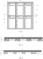
- FIG. 1 a is a schematic plan view of a display substrate provided by at least one embodiment of the present disclosure.
- FIG. 2 b is a second schematic sectional view of the display substrate, which includes the light source, provided by at least one embodiment of the present disclosure.
- FIG. 3 a and FIG. 3 b are schematic structural views of a display device provided by at least one embodiment of the present disclosure in which a functional sensor and a black matrix sensor are successively arranged along a propagation direction of ambient light.
- FIG. 4 b is a schematic view illustrating a light path when the display device illustrated in FIG. 4 a is touched.
- FIG. 5 is a schematic structural view of the display device, which includes the light source and a back light source, provided by at least one embodiment of the present disclosure.
- FIG. 9 is a schematic sectional view of a fingerprint recognition device provided by at least one embodiment of the present disclosure.
- first signal lines 81 , second signal lines 82 and third signal lines 83 are provided on the base substrate 10 ; and each of the switch elements 90 , for example, is a transistor, and a source electrode of the transistor is connected with a corresponding first signal line 81 , a gate electrode of the transistor is connected with a corresponding second signal line 82 , a drain electrode is connected with a corresponding functional sensor 30 , and the output terminal of the functional sensor 30 is connected with a corresponding third signal line 83 to output a signal through the third signal line 83 .
- the position relationship of the first signal line, the second signal line and the third second signal line in FIG. 1 a is only illustrative, and embodiments of the present disclosure include, but are not limited to, the structure shown in FIG. 1 a.
- the black matrix sensor 20 is light-tight, in this way, besides the visible light, the black matrix sensor 20 also blocks the light of other wavelengths, and thus the interference caused by that the visible light and the light of other wavelengths are sensed by the functional sensors 30 is avoided.
- the first electrode 21 is made of one or several kinds of transparent conductive materials such as indium tin oxide, indium zinc oxide and indium gallium zinc oxide.
- the semiconductor layer 23 has a structure of PIN or a structure of NIP, and as illustrated in FIG. 3 a and FIG. 3 b , the semiconductor layer 23 includes a P-type semiconductor layer 231 , an intrinsic semiconductor layer 233 and an N-type semiconductor 232 , which are arranged successively. It should be noted that the position of the P-type semiconductor layer 231 and the position of the N-type semiconductor layer 232 are interchangeable.
- the intrinsic semiconductor layer 233 includes a plurality of semiconductor sub-layers with different band gaps to broaden the absorption spectrum of the intrinsic semiconductor layer 233 and enhance the light-blocking effect of the black matrix sensor 20 .
- the semiconductor layer 35 is made of an organic semiconductor material or an inorganic semiconductor material, and the organic semiconductor material or the inorganic semiconductor material is sensitive to light of predetermined wavelengths.
- the display substrate provided by at least one embodiment of the present disclosure can also be an array substrate including a plurality of pixel electrodes or a plurality of light-emitting units (for example, organic light emitting diodes), as illustrated in FIG. 3 b ; and in this case, along a direction perpendicular to the base substrate 10 , the black matrix sensor 20 is between the functional sensors 30 and the base substrate 10 .
- a plurality of pixel electrodes or a plurality of light-emitting units for example, organic light emitting diodes
- the functional sensors 30 are used as touch control sensors for realizing a function of touch control; or the functional sensors 30 are used as fingerprint recognition sensors for realizing a function of fingerprint recognition; or the functional sensors are sensors for realizing other functions.
- the functional sensors are capacitive, resistive, ultrasonic, or optical sensors or pressure sensors.
- the functional sensors 30 are optical sensors.
- the functional sensors 30 which are optical sensors are used to absorb the reflection light at a touch positon and produce a light current, and the touch position is positioned or a fingerprint is recognized according to the light current.
- the black matrix sensor 20 is light-tight, in this way, besides visible light, the black matrix sensor 20 also blocks the light of other wavelengths, and thus the interference caused by that the visible light and the light of other wavelengths are sensed by the functional sensors 30 is avoided.
- the semiconductor layer 36 is made of an organic semiconductor material or an inorganic semiconductor material which is sensitive to light of predetermined wavelengths.
- the semiconductor layer 23 includes a P-type semiconductor layer, an intrinsic semiconductor layer and an N-type semiconductor, which are arranged successively, a material of the intrinsic semiconductor layer is an amorphous silicon semiconductor, and a thickness of the intrinsic semiconductor layer is larger than 1 micron.
- the semiconductor layer 23 includes a P-type semiconductor layer 231 , an intrinsic semiconductor layer 233 and an N-type semiconductor 232 , which are arranged successively.
- the black matrix sensor 20 in a case where the black matrix sensor 20 is an optical sensor, the black matrix sensor 20 is used as a solar battery, and by connecting the black matrix sensor 20 with the light source 50 ′ (for example, an infrared LED (light-emitting diode)), the light source 50 ′ can emit light and thus the light source 50 ′ needs no additional power source.
- the light source 50 ′ for example, an infrared LED (light-emitting diode)
- the light source 50 ′ can emit light and thus the light source 50 ′ needs no additional power source.
- the light source 50 ′ is formed on the opposite substrate 01 ′, and the light source 50 ′ is in the non-display region or in the display region to realize a touch detection or a fingerprint recognition of high signal-noise ratio.
- the black matrix sensor 20 is an optical sensor
- the current produced by the black matrix sensor 20 changes with the change of the ambient light
- the black matrix sensor 20 by connecting the black matrix sensor 20 with the back light source 70 , the brightness of the back light source 70 is controlled by utilizing the black matrix sensor 20 .
- the fingerprint recognition device includes a plurality of fingerprint recognition sensors 30 A which are spaced apart from each other and a black matrix sensor 20 which blocks at least visible light.
- the structure of the black matrix sensor 20 can be referred to the related description in the embodiments of the display substrate 01 .
- the black matrix sensor 20 includes a plurality of first extension portions 21 and a plurality of second extension portions 22 , and the first extension portions 21 intersect the second extension portions 22 to form a plurality of hollow regions 23 . Orthographic projections of the fingerprint recognition sensors 30 A on the black matrix sensor 20 are within a region where the black matrix sensor 20 is located.
Landscapes
- Physics & Mathematics (AREA)
- Engineering & Computer Science (AREA)
- General Physics & Mathematics (AREA)
- Power Engineering (AREA)
- Nonlinear Science (AREA)
- Condensed Matter Physics & Semiconductors (AREA)
- Microelectronics & Electronic Packaging (AREA)
- Computer Hardware Design (AREA)
- Chemical & Material Sciences (AREA)
- Crystallography & Structural Chemistry (AREA)
- Mathematical Physics (AREA)
- Optics & Photonics (AREA)
- Electromagnetism (AREA)
- Multimedia (AREA)
- Theoretical Computer Science (AREA)
- Human Computer Interaction (AREA)
- Materials Engineering (AREA)
- Nanotechnology (AREA)
- Devices For Indicating Variable Information By Combining Individual Elements (AREA)
Applications Claiming Priority (4)
| Application Number | Priority Date | Filing Date | Title |
|---|---|---|---|
| CN201611091448.4 | 2016-12-01 | ||
| CN201611091448.4A CN106373969B (zh) | 2016-12-01 | 2016-12-01 | 显示基板和显示装置 |
| CN201611091448 | 2016-12-01 | ||
| PCT/CN2017/103961 WO2018099176A1 (zh) | 2016-12-01 | 2017-09-28 | 显示基板及其制作方法、指纹识别装置和显示装置 |
Publications (2)
| Publication Number | Publication Date |
|---|---|
| US20190280039A1 US20190280039A1 (en) | 2019-09-12 |
| US10872922B2 true US10872922B2 (en) | 2020-12-22 |
Family
ID=57892483
Family Applications (1)
| Application Number | Title | Priority Date | Filing Date |
|---|---|---|---|
| US15/776,984 Active 2038-08-11 US10872922B2 (en) | 2016-12-01 | 2017-09-28 | Display substrate and method for manufacturing the same, fingerprint recognition device and display device |
Country Status (3)
| Country | Link |
|---|---|
| US (1) | US10872922B2 (zh) |
| CN (1) | CN106373969B (zh) |
| WO (1) | WO2018099176A1 (zh) |
Cited By (1)
| Publication number | Priority date | Publication date | Assignee | Title |
|---|---|---|---|---|
| US11495176B1 (en) | 2020-05-21 | 2022-11-08 | Apple Inc. | Methods and configurations for improving the performance of sensors under a display |
Families Citing this family (33)
| Publication number | Priority date | Publication date | Assignee | Title |
|---|---|---|---|---|
| CN106373532B (zh) * | 2016-10-27 | 2019-01-11 | 合肥京东方显示技术有限公司 | 一种阵列基板、电润湿显示面板及显示装置 |
| CN106373969B (zh) * | 2016-12-01 | 2019-10-29 | 京东方科技集团股份有限公司 | 显示基板和显示装置 |
| CN106898578B (zh) | 2017-03-30 | 2019-08-06 | 合肥鑫晟光电科技有限公司 | 一种显示基板的制备方法、阵列基板及显示装置 |
| US10664676B2 (en) * | 2017-06-12 | 2020-05-26 | Will Semiconductor (Shanghai) Co. Ltd. | Systems and methods for reducing unwanted reflections in display systems incorporating an under display biometric sensor |
| CN107392160B (zh) | 2017-07-27 | 2021-10-26 | 北京小米移动软件有限公司 | 光学指纹识别方法及装置、计算机可读存储介质 |
| CN107357079A (zh) | 2017-08-29 | 2017-11-17 | 惠科股份有限公司 | 一种显示面板 |
| CN108365050B (zh) * | 2018-02-24 | 2019-11-05 | 京东方科技集团股份有限公司 | 一种传感器及其制作方法、显示面板及显示装置 |
| CN108646454A (zh) * | 2018-03-13 | 2018-10-12 | 东旭(昆山)显示材料有限公司 | 彩膜基板、彩膜基板的制备方法和显示面板 |
| CN108598111B (zh) * | 2018-04-24 | 2021-01-29 | 京东方科技集团股份有限公司 | 具有指纹识别功能的显示基板、方法及显示装置 |
| CN108710237B (zh) * | 2018-04-27 | 2022-08-12 | 厦门天马微电子有限公司 | 显示面板及显示装置 |
| CN108806603B (zh) * | 2018-06-29 | 2020-03-17 | 上海天马有机发光显示技术有限公司 | 一种有机发光显示面板及其驱动方法、有机发光显示装置 |
| CN109190563B (zh) * | 2018-09-05 | 2022-02-25 | 京东方科技集团股份有限公司 | 显示面板及其制备方法、显示装置 |
| CN111386614B (zh) | 2018-11-01 | 2023-04-04 | 京东方科技集团股份有限公司 | 发光二极管及其制造方法、阵列基板和显示面板 |
| CN111243506B (zh) * | 2018-11-29 | 2021-11-02 | 北京小米移动软件有限公司 | 屏幕亮度调整方法、装置、设备及存储介质 |
| CN109545837B (zh) * | 2018-12-17 | 2020-10-13 | 武汉华星光电半导体显示技术有限公司 | Amoled柔性显示装置 |
| CN109856853B (zh) * | 2019-04-04 | 2022-05-24 | 京东方科技集团股份有限公司 | 彩膜基板及液晶显示器 |
| CN111052143B (zh) * | 2019-04-10 | 2023-09-08 | 深圳市汇顶科技股份有限公司 | 光学指纹装置和电子设备 |
| CN110222600A (zh) | 2019-05-22 | 2019-09-10 | 武汉华星光电技术有限公司 | 显示面板和电子设备 |
| CN110222620A (zh) * | 2019-05-30 | 2019-09-10 | 武汉华星光电技术有限公司 | 一种显示面板 |
| US11049992B2 (en) * | 2019-07-11 | 2021-06-29 | Pix Art Imaging Inc. | Dual wavelength light emitting device, dual wavelength light transceiving device and display |
| CN110678983B (zh) * | 2019-08-20 | 2022-05-31 | 京东方科技集团股份有限公司 | 阵列基板、显示设备和制造阵列基板的方法 |
| JP7461725B2 (ja) * | 2019-09-12 | 2024-04-04 | 株式会社ジャパンディスプレイ | 検出装置 |
| CN110991400B (zh) * | 2019-12-18 | 2023-08-18 | 京东方科技集团股份有限公司 | 一种显示基板及其制备方法、显示装置 |
| CN111025709A (zh) * | 2019-12-23 | 2020-04-17 | 厦门天马微电子有限公司 | 显示面板和显示装置 |
| JP7460392B2 (ja) * | 2020-02-26 | 2024-04-02 | 株式会社ジャパンディスプレイ | 光センサ装置 |
| CN111312780B (zh) * | 2020-02-27 | 2022-12-23 | 深圳市华星光电半导体显示技术有限公司 | 一种具有高开口率的显示面板及其制作方法和显示装置 |
| CN111258141A (zh) | 2020-03-06 | 2020-06-09 | Tcl华星光电技术有限公司 | 显示面板、显示装置 |
| US11273757B2 (en) * | 2020-03-20 | 2022-03-15 | B/E Aerospace, Inc. | Aircraft emergency lighting system |
| CN113777819B (zh) | 2020-06-09 | 2023-06-06 | 京东方科技集团股份有限公司 | 显示面板和显示装置 |
| CN111708202B (zh) * | 2020-07-17 | 2023-12-01 | 京东方科技集团股份有限公司 | 一种显示面板和显示装置 |
| US12008831B2 (en) * | 2020-08-27 | 2024-06-11 | Au Optronics Corporation | Sensing device substrate and display apparatus having the same |
| CN115016157A (zh) | 2021-03-03 | 2022-09-06 | 群创光电股份有限公司 | 显示装置 |
| CN114063341B (zh) * | 2021-12-03 | 2023-09-19 | 京东方科技集团股份有限公司 | 一种显示面板及显示装置 |
Citations (17)
| Publication number | Priority date | Publication date | Assignee | Title |
|---|---|---|---|---|
| JP2000019983A (ja) | 1998-07-07 | 2000-01-21 | Sharp Corp | 画像表示装置 |
| US20130044384A1 (en) | 2011-08-19 | 2013-02-21 | Samsung Electro-Mechanics Co., Ltd. | Color filter substrate embedded with touch sensor and method for manufacturing the same |
| US20140098305A1 (en) * | 2012-09-26 | 2014-04-10 | Focaltech Systems, Ltd. | Lcd touch screen and applications integrating single layer capacitive sensor |
| US20150198852A1 (en) * | 2014-01-15 | 2015-07-16 | Samsung Display Co., Ltd | Liquid crystal display |
| CN105678255A (zh) | 2016-01-04 | 2016-06-15 | 京东方科技集团股份有限公司 | 一种光学式指纹识别显示屏及显示装置 |
| CN205334402U (zh) | 2015-07-10 | 2016-06-22 | 宸鸿科技(厦门)有限公司 | 一种压力感测输入装置 |
| US20160216799A1 (en) * | 2015-01-26 | 2016-07-28 | Boe Technology Group Co., Ltd. | Self-capacitive touch screen and display device |
| WO2016148106A1 (ja) | 2015-03-17 | 2016-09-22 | シャープ株式会社 | カラーフィルター基板、センサー基板、及び表示装置 |
| CN106201147A (zh) | 2016-07-26 | 2016-12-07 | 京东方科技集团股份有限公司 | 触控基板及显示装置 |
| CN106325582A (zh) | 2015-07-10 | 2017-01-11 | 宸鸿科技(厦门)有限公司 | 一种具有压力侦测的触控总成及其驱动方法 |
| US20170082894A1 (en) * | 2014-05-21 | 2017-03-23 | Sharp Kabushiki Kaisha | Liquid crystal display device, optical control member, and base material for manufacturing optical control member |
| CN106559492A (zh) | 2016-11-30 | 2017-04-05 | 努比亚技术有限公司 | 基于压力补偿的功能执行方法及系统 |
| US20180231827A1 (en) * | 2017-02-10 | 2018-08-16 | Microsoft Technology Licensing, Llc | Black matrix structures for display devices |
| US20190056613A1 (en) * | 2017-02-07 | 2019-02-21 | Boe Technology Group Co., Ltd. | Display device |
| US20190115411A1 (en) * | 2017-10-16 | 2019-04-18 | Samsung Display Co., Ltd. | Display device |
| US20190353833A1 (en) * | 2017-05-17 | 2019-11-21 | Beijing Boe Optoelectronics Technology Co., Ltd. | Color film substrate, method for manufacturing the same, and display device |
| US20200105844A1 (en) * | 2018-09-30 | 2020-04-02 | Boe Technology Group Co., Ltd. | Oled substrate, manufacturing method thereof, transparent display |
Family Cites Families (6)
| Publication number | Priority date | Publication date | Assignee | Title |
|---|---|---|---|---|
| US20110221697A1 (en) * | 2008-11-25 | 2011-09-15 | Sharp Kabushiki Kaisha | Liquid crystal display device and method for manufacturing the liquid crystal display device |
| US20120320307A1 (en) * | 2010-02-18 | 2012-12-20 | Sharp Kabushiki Kaisha | Active matrix substrate, glass substrate, liquid crystal panel and liquid crystal display device |
| CN103887316B (zh) * | 2012-12-21 | 2017-04-12 | 上海天马微电子有限公司 | 一种图像传感器 |
| CN104881196B (zh) * | 2015-06-23 | 2018-04-20 | 京东方科技集团股份有限公司 | 基板及显示屏 |
| CN106094320B (zh) * | 2016-06-21 | 2019-03-26 | 武汉华星光电技术有限公司 | 彩膜基板及液晶显示装置 |
| CN106373969B (zh) * | 2016-12-01 | 2019-10-29 | 京东方科技集团股份有限公司 | 显示基板和显示装置 |
-
2016
- 2016-12-01 CN CN201611091448.4A patent/CN106373969B/zh active Active
-
2017
- 2017-09-28 US US15/776,984 patent/US10872922B2/en active Active
- 2017-09-28 WO PCT/CN2017/103961 patent/WO2018099176A1/zh active Application Filing
Patent Citations (18)
| Publication number | Priority date | Publication date | Assignee | Title |
|---|---|---|---|---|
| JP2000019983A (ja) | 1998-07-07 | 2000-01-21 | Sharp Corp | 画像表示装置 |
| US20130044384A1 (en) | 2011-08-19 | 2013-02-21 | Samsung Electro-Mechanics Co., Ltd. | Color filter substrate embedded with touch sensor and method for manufacturing the same |
| US20140098305A1 (en) * | 2012-09-26 | 2014-04-10 | Focaltech Systems, Ltd. | Lcd touch screen and applications integrating single layer capacitive sensor |
| US20150198852A1 (en) * | 2014-01-15 | 2015-07-16 | Samsung Display Co., Ltd | Liquid crystal display |
| US20170082894A1 (en) * | 2014-05-21 | 2017-03-23 | Sharp Kabushiki Kaisha | Liquid crystal display device, optical control member, and base material for manufacturing optical control member |
| US20160216799A1 (en) * | 2015-01-26 | 2016-07-28 | Boe Technology Group Co., Ltd. | Self-capacitive touch screen and display device |
| WO2016148106A1 (ja) | 2015-03-17 | 2016-09-22 | シャープ株式会社 | カラーフィルター基板、センサー基板、及び表示装置 |
| CN106325582A (zh) | 2015-07-10 | 2017-01-11 | 宸鸿科技(厦门)有限公司 | 一种具有压力侦测的触控总成及其驱动方法 |
| CN205334402U (zh) | 2015-07-10 | 2016-06-22 | 宸鸿科技(厦门)有限公司 | 一种压力感测输入装置 |
| US20180211085A1 (en) | 2016-01-04 | 2018-07-26 | Boe Technology Group Co., Ltd. | Optical fingerprint identification display screen and display device |
| CN105678255A (zh) | 2016-01-04 | 2016-06-15 | 京东方科技集团股份有限公司 | 一种光学式指纹识别显示屏及显示装置 |
| CN106201147A (zh) | 2016-07-26 | 2016-12-07 | 京东方科技集团股份有限公司 | 触控基板及显示装置 |
| CN106559492A (zh) | 2016-11-30 | 2017-04-05 | 努比亚技术有限公司 | 基于压力补偿的功能执行方法及系统 |
| US20190056613A1 (en) * | 2017-02-07 | 2019-02-21 | Boe Technology Group Co., Ltd. | Display device |
| US20180231827A1 (en) * | 2017-02-10 | 2018-08-16 | Microsoft Technology Licensing, Llc | Black matrix structures for display devices |
| US20190353833A1 (en) * | 2017-05-17 | 2019-11-21 | Beijing Boe Optoelectronics Technology Co., Ltd. | Color film substrate, method for manufacturing the same, and display device |
| US20190115411A1 (en) * | 2017-10-16 | 2019-04-18 | Samsung Display Co., Ltd. | Display device |
| US20200105844A1 (en) * | 2018-09-30 | 2020-04-02 | Boe Technology Group Co., Ltd. | Oled substrate, manufacturing method thereof, transparent display |
Non-Patent Citations (3)
| Title |
|---|
| First Chinese Office Action dated Oct. 15, 2018. |
| International Search Report dated Jan. 4, 2018. |
| Second Chinese Office Action dated May 8, 2019. |
Cited By (1)
| Publication number | Priority date | Publication date | Assignee | Title |
|---|---|---|---|---|
| US11495176B1 (en) | 2020-05-21 | 2022-11-08 | Apple Inc. | Methods and configurations for improving the performance of sensors under a display |
Also Published As
| Publication number | Publication date |
|---|---|
| US20190280039A1 (en) | 2019-09-12 |
| CN106373969B (zh) | 2019-10-29 |
| CN106373969A (zh) | 2017-02-01 |
| WO2018099176A1 (zh) | 2018-06-07 |
Similar Documents
| Publication | Publication Date | Title |
|---|---|---|
| US10872922B2 (en) | Display substrate and method for manufacturing the same, fingerprint recognition device and display device | |
| KR102655476B1 (ko) | 유기발광 표시장치 | |
| WO2018126644A1 (zh) | 指纹识别装置及电子设备 | |
| US11232750B2 (en) | Display substrate, display panel, and manufacturing method and driving method of display substrate | |
| US8368068B2 (en) | Display with photo sensor and manufacturing method thereof | |
| WO2017008481A1 (zh) | 显示装置和阵列基板 | |
| US11301707B2 (en) | Texture recognition device and driving method of texture recognition device | |
| US20210271844A1 (en) | Flexible display panel with fingerprint identification | |
| KR101790161B1 (ko) | 광 센서, 광 센서의 제조 방법, 및 광 센서를 포함하는 액정 표시 장치 | |
| TW201334178A (zh) | 有機電激發光元件的畫素結構 | |
| US10964763B2 (en) | Display panel, manufacturing method thereof, and display device | |
| US12062248B2 (en) | Display panel and display device | |
| WO2020232637A1 (zh) | 纹路识别装置及其制造方法、彩膜基板及其制造方法 | |
| TWI413829B (zh) | 反射式觸控顯示面板及其製造方法 | |
| JP2024513414A (ja) | ディスプレイパネル、ディスプレイモジュール、および電子デバイス | |
| WO2021204093A1 (zh) | 一种显示屏和电子设备 | |
| US10884552B2 (en) | Touch panel with sensor elements | |
| CN114299823B (zh) | 显示面板及其制备方法、光检测方法、显示装置 | |
| WO2021238139A1 (zh) | 传感器、显示面板及显示装置 | |
| WO2021238138A1 (zh) | 传感器、显示面板及显示装置 | |
| US11580771B2 (en) | Image capturing apparatus | |
| WO2022165827A1 (zh) | 触控面板结构及包含所述触控面板结构的触控显示设备 | |
| CN114442316B (zh) | 一种显示模组及其制作方法、头戴式显示设备 | |
| TWI712027B (zh) | 顯示面板 | |
| CN112928173A (zh) | 感光传感器、感光传感器的制作方法以及显示面板 |
Legal Events
| Date | Code | Title | Description |
|---|---|---|---|
| AS | Assignment |
Owner name: BOE TECHNOLOGY GROUP CO., LTD., CHINA Free format text: ASSIGNMENT OF ASSIGNORS INTEREST;ASSIGNORS:JIA, YANAN;DONG, XUE;LV, JING;AND OTHERS;REEL/FRAME:046180/0106 Effective date: 20180314 |
|
| FEPP | Fee payment procedure |
Free format text: ENTITY STATUS SET TO UNDISCOUNTED (ORIGINAL EVENT CODE: BIG.); ENTITY STATUS OF PATENT OWNER: LARGE ENTITY |
|
| STPP | Information on status: patent application and granting procedure in general |
Free format text: RESPONSE TO NON-FINAL OFFICE ACTION ENTERED AND FORWARDED TO EXAMINER |
|
| STPP | Information on status: patent application and granting procedure in general |
Free format text: PUBLICATIONS -- ISSUE FEE PAYMENT VERIFIED |
|
| STCF | Information on status: patent grant |
Free format text: PATENTED CASE |
|
| MAFP | Maintenance fee payment |
Free format text: PAYMENT OF MAINTENANCE FEE, 4TH YEAR, LARGE ENTITY (ORIGINAL EVENT CODE: M1551); ENTITY STATUS OF PATENT OWNER: LARGE ENTITY Year of fee payment: 4 |