US10778210B2 - Load driver - Google Patents
Load driver Download PDFInfo
- Publication number
- US10778210B2 US10778210B2 US16/274,596 US201916274596A US10778210B2 US 10778210 B2 US10778210 B2 US 10778210B2 US 201916274596 A US201916274596 A US 201916274596A US 10778210 B2 US10778210 B2 US 10778210B2
- Authority
- US
- United States
- Prior art keywords
- switching element
- mos
- control circuit
- voltage
- gate
- Prior art date
- Legal status (The legal status is an assumption and is not a legal conclusion. Google has not performed a legal analysis and makes no representation as to the accuracy of the status listed.)
- Active
Links
- 238000001514 detection method Methods 0.000 claims abstract description 100
- 238000010992 reflux Methods 0.000 abstract description 111
- 230000003071 parasitic effect Effects 0.000 abstract description 10
- 150000003272 mannan oligosaccharides Chemical class 0.000 description 348
- 101710132461 Molybdenum cofactor sulfurase Proteins 0.000 description 268
- 238000000034 method Methods 0.000 description 94
- 230000008569 process Effects 0.000 description 91
- 230000002265 prevention Effects 0.000 description 12
- 239000003990 capacitor Substances 0.000 description 7
- 239000000446 fuel Substances 0.000 description 7
- 230000006870 function Effects 0.000 description 7
- 238000002347 injection Methods 0.000 description 5
- 239000007924 injection Substances 0.000 description 5
- 230000000694 effects Effects 0.000 description 4
- 230000001939 inductive effect Effects 0.000 description 3
- 230000004048 modification Effects 0.000 description 3
- 238000012986 modification Methods 0.000 description 3
- 238000012544 monitoring process Methods 0.000 description 3
- 230000002159 abnormal effect Effects 0.000 description 2
- 230000008901 benefit Effects 0.000 description 2
- 230000007423 decrease Effects 0.000 description 2
- 230000003247 decreasing effect Effects 0.000 description 2
- 238000003745 diagnosis Methods 0.000 description 2
- 238000010586 diagram Methods 0.000 description 2
- 230000006872 improvement Effects 0.000 description 2
- 230000007704 transition Effects 0.000 description 2
- -1 “YES Chemical class 0.000 description 2
- 101710116852 Molybdenum cofactor sulfurase 1 Proteins 0.000 description 1
- 230000005856 abnormality Effects 0.000 description 1
- 230000015572 biosynthetic process Effects 0.000 description 1
- 238000002485 combustion reaction Methods 0.000 description 1
- 238000007599 discharging Methods 0.000 description 1
- 230000005669 field effect Effects 0.000 description 1
- 238000005755 formation reaction Methods 0.000 description 1
- 230000020169 heat generation Effects 0.000 description 1
- 230000002028 premature Effects 0.000 description 1
- 230000008929 regeneration Effects 0.000 description 1
- 238000011069 regeneration method Methods 0.000 description 1
- 239000004065 semiconductor Substances 0.000 description 1
Images


Classifications
-
- H—ELECTRICITY
- H03—ELECTRONIC CIRCUITRY
- H03K—PULSE TECHNIQUE
- H03K17/00—Electronic switching or gating, i.e. not by contact-making and –breaking
- H03K17/08—Modifications for protecting switching circuit against overcurrent or overvoltage
- H03K17/082—Modifications for protecting switching circuit against overcurrent or overvoltage by feedback from the output to the control circuit
- H03K17/0822—Modifications for protecting switching circuit against overcurrent or overvoltage by feedback from the output to the control circuit in field-effect transistor switches
-
- H—ELECTRICITY
- H03—ELECTRONIC CIRCUITRY
- H03K—PULSE TECHNIQUE
- H03K17/00—Electronic switching or gating, i.e. not by contact-making and –breaking
- H03K17/08—Modifications for protecting switching circuit against overcurrent or overvoltage
- H03K17/081—Modifications for protecting switching circuit against overcurrent or overvoltage without feedback from the output circuit to the control circuit
- H03K17/08104—Modifications for protecting switching circuit against overcurrent or overvoltage without feedback from the output circuit to the control circuit in field-effect transistor switches
-
- F—MECHANICAL ENGINEERING; LIGHTING; HEATING; WEAPONS; BLASTING
- F16—ENGINEERING ELEMENTS AND UNITS; GENERAL MEASURES FOR PRODUCING AND MAINTAINING EFFECTIVE FUNCTIONING OF MACHINES OR INSTALLATIONS; THERMAL INSULATION IN GENERAL
- F16K—VALVES; TAPS; COCKS; ACTUATING-FLOATS; DEVICES FOR VENTING OR AERATING
- F16K31/00—Actuating devices; Operating means; Releasing devices
- F16K31/02—Actuating devices; Operating means; Releasing devices electric; magnetic
- F16K31/06—Actuating devices; Operating means; Releasing devices electric; magnetic using a magnet, e.g. diaphragm valves, cutting off by means of a liquid
- F16K31/0675—Electromagnet aspects, e.g. electric supply therefor
-
- H—ELECTRICITY
- H03—ELECTRONIC CIRCUITRY
- H03K—PULSE TECHNIQUE
- H03K17/00—Electronic switching or gating, i.e. not by contact-making and –breaking
- H03K17/08—Modifications for protecting switching circuit against overcurrent or overvoltage
- H03K17/081—Modifications for protecting switching circuit against overcurrent or overvoltage without feedback from the output circuit to the control circuit
- H03K17/0812—Modifications for protecting switching circuit against overcurrent or overvoltage without feedback from the output circuit to the control circuit by measures taken in the control circuit
- H03K17/08122—Modifications for protecting switching circuit against overcurrent or overvoltage without feedback from the output circuit to the control circuit by measures taken in the control circuit in field-effect transistor switches
-
- H—ELECTRICITY
- H03—ELECTRONIC CIRCUITRY
- H03K—PULSE TECHNIQUE
- H03K17/00—Electronic switching or gating, i.e. not by contact-making and –breaking
- H03K17/51—Electronic switching or gating, i.e. not by contact-making and –breaking characterised by the components used
- H03K17/56—Electronic switching or gating, i.e. not by contact-making and –breaking characterised by the components used by the use, as active elements, of semiconductor devices
- H03K17/687—Electronic switching or gating, i.e. not by contact-making and –breaking characterised by the components used by the use, as active elements, of semiconductor devices the devices being field-effect transistors
-
- H—ELECTRICITY
- H03—ELECTRONIC CIRCUITRY
- H03K—PULSE TECHNIQUE
- H03K2217/00—Indexing scheme related to electronic switching or gating, i.e. not by contact-making or -breaking covered by H03K17/00
- H03K2217/0027—Measuring means of, e.g. currents through or voltages across the switch
Definitions
- the present disclosure relates to a load driver or a load driving device for driving an electrical load.
- Load drivers for driving an electrical load may be configured as control circuits having small volumes and high functionality, yet be subject problems. As such, load drivers are subject to improvement.
- the present disclosure describes a load driver that is capable of monitoring a gate terminal potential without increasing the number of terminals of its control section.
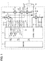
- FIG. 1 is a schematic diagram of a load driver in a first embodiment of the present disclosure
- FIG. 2 is a flowchart of an operation of the load driver:
- FIG. 3 is another flowchart of the operation of the load driver:
- FIG. 4 is a timing chart of the operation of the load driver
- FIG. 5 illustrates operational effects of the load driver
- FIG. 6 is a flowchart of an operation of a load driver in a second embodiment of the present disclosure
- FIG. 7 is another flowchart of the operation of the load driver in the second embodiment:
- FIG. 8 illustrates operational effects of the load driver in the second embodiment
- FIG. 9 is a flowchart of an operation of the load driver in a third embodiment of the present disclosure.
- Load drivers for driving an electrical load may be configured as control circuits having small volumes and high functionality, yet be subject to heat generation problems.
- a large amount of heat may be generated from a driver device for driving a fuel injector in a vehicle.
- the driver may generate heat from a diode that serves as a supply current path and a regeneration current path. Consequently, the diode may be replaced by a switching element such as MOSFET to implement a synchronously-commutated method of current supply.
- the synchronously-commutated current supply method using a switching element having three terminals such as a MOSFET may detect a ground fault abnormality at a gate terminal of the switching element by monitoring the gate terminal potential.
- Such monitoring increases the cost of the load driver by requiring an extra, monitor terminal (i.e., an extra pin) in a load driver integrated circuit (IC).
- load drivers are subject to improvement.
- a load driver may be of a synchronous-commutated type, which is configured to supply an electric current to an electro-magnetic valve by an ON-OFF drive of (i) a gate-drive type first switching element for a power supply, and (ii) a gate-drive type second switching element for a return current (i.e., reflux current, or more simply, reflux) under the control of a control circuit.
- the load driver may include the first switching element, the second switching element, and the control circuit for such an ON-OFF drive of the first and second switching elements.
- the control circuit of the load driver may determine a gate ground fault of the second switching element when an inter-terminal voltage of the second switching element at a time of a gate-ON drive of the second switching element is equal to or lower than a threshold voltage that is set to be lower than a normal gate-ON drive time.
- the load driver implementing the synchronously-commutated method may allow a return current generated in the electromagnetic valve to flow by an ON drive of the second switching element after an ON drive of the first switching element.
- the load driver may enable its control circuit to determine the gate ground fault of the second switching element by detecting that the inter-terminal voltage of the second switching element at the gate-ON drive time is equal to or lower than the threshold voltage that is set to be lower than a normal gate-ON drive time. Consequently, such configuration requires no additional terminal in the control circuit for the determination of the gate ground fault of the second switching element.
- FIG. 1 shows an electrical configuration of a load driving device 1 for injecting fuel to an internal-combustion engine.
- the load driving device 1 drives an electromagnetic valve 2 (e.g., a solenoid valve 2 ) that is an inductive load.
- an electromagnetic valve 2 e.g., a solenoid valve 2
- the load driving device 1 is driven and controlled by the control circuit 3 that operates according to instructions from a computer 4 .
- the computer 4 may be a small-sized computer such as a microcontroller or a system on a chip (SoC).
- the computer 4 may include one or more CPUs (i.e., processor cores); memory such as RAM, ROM, flash; and input/output (I/O) (all not shown).
- the memory may be used to store a program/instruction set and the memory is an example of a substantive, non-transitory computer readable medium.
- the one or more CPUs of the computer 4 may execute a program/instruction set stored in memory to instruct the control circuit 3 for performing the processes described in greater detail below associated with the control circuit 3 .
- control circuit 3 may perform the processes, for example, associated with the process flow diagrams shown in FIGS. 2 and 3 (as well as in FIGS. 6, 7, and 9 in the other embodiments).
- the control circuit 3 may also contain its own computing device (not shown) for performing the processes associated with the control circuit 3 .
- the computer 4 may be included in the control circuit 3 .
- Two terminals of the solenoid valve 2 are respectively connected to the load driving device at output terminals A and B of the load driving device 1 .
- Electric power also referred to simply as “power” throughout the description, is supplied from two power sources for driving the solenoid valve 2 . That is, power may be supplied from both a direct current (DC) power source VB connected to a positive electrode terminal of an in-vehicle battery and a high voltage power source VH that is boosted from the direct current power source VB via a booster circuit.
- the DC power source may also be, for example, the vehicle battery itself.
- the high voltage power source VH is connected to the output terminal A via a switching element 5 .
- the switching element 5 may be a metal-oxide-semiconductor field-effect transistor and also be referred to as a discharge MOS 5 .
- the discharge MOS 5 may be implemented as an N-channel or n-type MOSFET.
- the output terminal B is connected to ground (e.g., a return path) via a switching element 6 and a resistor 7 connected in series.
- the switching element 6 may be referred to as a cylinder MOS 6 and be implemented as an n-type MOSFET.
- Built-in parasitic diodes 5 a and 6 a are respectively incorporated in the discharge MOS 5 and the cylinder MOS 6 .
- the output terminal A is connected to ground via a switching element 8 .
- the switching element 8 may be referred to as a reflux MOS 8 and be implemented as an N-channel type MOSFET.
- the reflux MOS 8 incorporates a built-in parasitic diode 8 a .
- a capacitor 9 is connected at a position between the output terminal B and the ground.
- a capacitor 10 is connected in parallel with the resistor 7 .
- the DC power source VB is connected to the output terminal A via a series connection of switching elements 11 and 12 .
- the switching element 11 may be referred to as a constant-current MOS 11 and be implemented as an n-type MOSFET.
- the switching element 12 may be referred to as a backflow prevention MOS 12 and be implemented as an N-channel type MOSFET.
- the constant-current MOS 11 and the backflow prevention MOS 12 have their sources connected to each other.
- Built-in parasitic diodes 11 a and 12 a are respectively incorporated into the constant-current MOS 11 and the backflow prevention MOS 12 .
- a diode 13 is connected in a forward direction from the output terminal B to the high voltage power source VH. That is, the anode of the diode 13 is connected to the output terminal B and the cathode of the diode 13 is connected to the high voltage power source VH.
- the discharge MOS 5 and the constant-current MOS 11 respectively function as a first switching element, where the discharge MOS 5 functions as a high-voltage switching element and the constant-current MOS 11 functions as a normal switching element.
- the reflux MOS 8 functions as a second switching element.
- the discharge MOS 5 , cylinder MOS 6 , reflux MOS 8 , constant-current MOS 11 , and the backflow prevention MOS 12 are gate-drive type switching elements.
- the gate of the discharge MOS 5 is connected to the control circuit 3 via a resistor 14
- the gate of the cylinder MOS 6 is connected to the control circuit 3 via a resistor 15 .
- the control circuit 3 drives the discharge MOS 5 and the cylinder MOS 6 to supply power from the high voltage power source VH to the solenoid valve 2 .
- the gate of the reflux MOS 8 is connected to the control circuit 3 via a resistor 16 .
- the control circuit 3 drives the cylinder MOS 6 and the reflux MOS 8 to effectuate the flow of a return current from the solenoid valve 2 .
- the gate of the constant-current MOS 11 is connected to the control circuit 3 via a resistor 17
- the gate of the backflow prevention MOS 12 is connected to the control circuit 3 via a resistor 18 .
- the control circuit 3 drives the constant-current MOS 11 , the backflow prevention MOS 12 , and the cylinder MOS 6 to supply power from the DC power source VB.
- the control circuit 3 holds the backflow prevention MOS 12 in an OFF state to prevent the flow of current to or toward the DC power source VB.
- the source of the discharge MOS 5 is directly connected to the control circuit 3 and is also connected to the control circuit 3 via a resistor 19 and a capacitor 20 in series.
- Both the source of the constant-current MOS 11 and the backflow prevention MOS 12 collectively referred to as the “common” source, are connected directly to the control circuit 3 .
- the common source is also connected to the control circuit 3 via a resistor 21 and a capacitor 22 in series, and via a resistor 23 and a capacitor 24 connected in series.
- the three series circuits including the resistor and the capacitor respectively form a bootstrap circuit and are used for maintaining an ON state of the discharge MOS 5 and the constant-current MOS 11 .
- the control circuit 3 is internally provided with a fault detection circuit 30 .
- the fault detection circuit 30 includes a first comparator 31 for fault detection, a second comparator 32 , and a bias power source 33 .
- the fault detection circuit 30 is configured to detect a detection voltage VDS of the drain terminal (e.g., at the output terminal A) of the reflux MOS 8 for operating the MOS 8 as a reflux MOS.
- the detection voltage VDS is input to non-inverted input terminals.
- the first threshold voltage Vth 1 is input to the inverted terminal of the first comparator 31 and the second threshold voltage Vth 2 is input to the inverted terminal of the second comparator 32 .
- the first comparator 31 is provided for determining an overcurrent by comparing a sample, for example, the detection voltage, with the first threshold voltage Vth 1 , which is an overcurrent detection voltage.
- the second comparator 32 compares the detection voltage VDS with the second threshold voltage Vth 2 for gate-ground fault detection.
- the bias power source 33 applies a reference voltage Vs (e.g., 2.5 V) to the drain of the reflux MOS 8 .
- the control circuit 3 of the load driving device 1 performs a power supply control for fuel injection to the solenoid valve 2 and performs a valve opening operation.
- the control circuit 3 begins to drive the cylinder MOS 6 to ON at time t 1 , as shown in FIG. 4 at (e), and then begins to drive the discharge MOS 5 to ON shortly after time t 1 , as shown at FIG. 4 at (c).
- a current path is formed as a power supply path from the high-voltage power source VH through the discharge MOS 5 , the solenoid valve 2 , the cylinder MOS 6 , and the resistor 7 to energize the solenoid valve 2 .
- the high-voltage power source VH supplies power to feed the solenoid valve 2 by discharging an accumulated charge from a boosting capacitor. Consequently, as shown in FIG. 4 at (b), the solenoid valve 2 receives a flow of load current Id that gradually increases starting at time t 2 . At time t 3 , the solenoid valve 2 is driven to a predetermined position. In other words during a power supply cycle for supplying electric power to the electromagnetic solenoid valve 2 , the control circuit 3 may drive the discharge MOS 5 (i.e., the high-voltage switching element) to ON for a preset period Ton 1 from time t 2 to t 3 to provide power from the high voltage power source VH.
- the discharge MOS 5 i.e., the high-voltage switching element
- the control circuit 3 also drives the constant-current MOS 11 to ON.
- the output terminal A is at an electric potential close to the voltage of the high voltage power source VH even when the constant-current MOS 11 is turned ON. In such a case, no power is supplied from the DC power source VB and a reflux or return current is prevented from flowing back to the DC power source VB by the backflow prevention MOS 12 .
- the electric potential of the output terminal A is raised to be substantially the same voltage of the high voltage power source VH. As shown in FIG. 4 at (h), such a high voltage is significantly higher than the reference potential Vs.
- the control circuit 3 turns OFF the discharge MOS 5 .
- the load current Id flowing through the solenoid valve 2 stops due to an interruption of the power supply from the high voltage power source VH.
- the solenoid valve 2 is inductive, the load current Id flows from the ground via the diode 8 a of the reflux MOS 8 in the OFF state.
- the control circuit 3 turns ON the reflux MOS 8 as shown in FIG. 4 at (g).
- a current path shown by the dotted line originates from the ground via the reflux MOS 8 , the solenoid valve 2 , the cylinder MOS 6 , and the resistor 7 . Consequently, as shown in FIG. 4 at (b), the solenoid valve 2 has the load current Id continuously flowing through the solenoid valve 2 as a return current.
- the detection voltage VDS at the output terminal A (i.e., the drain-source voltage Vds of the reflux MOS 8 ) becomes a negative voltage that is lower than the ground level by the amount of voltage of the ON state reflux MOS 8 , that is, by the drain-source voltage Vds.
- the drain-source voltage Vds of the reflux MOS 8 may also be referred to as the inter-terminal voltage of the reflux MOS 8 or the inter-terminal voltage of the second switching element 8 .
- the inter-terminal voltage Vds may be the same as the detection voltage VDS.
- the detection voltage VDS Since the drain-source voltage Vds of the ON state reflux MOS 8 has a value obtained by multiplying an ON-resistance Ron by the load current Id, the detection voltage VDS, for example, has a level of about ⁇ 0.1 to ⁇ 0.3 V.
- the control circuit 3 may drive the constant-current MOS 11 ON a plurality of times for a preset period Ton 2 to supply a normal, lower voltage power from the normal power source VB to the electromagnetic solenoid valve 2 to maintain the operation of the electromagnetic solenoid valve 2 .
- the control circuit 3 is configured to perform a plurality of preset-period (i.e., Ton 2 ) drive maintaining operations of the normal switching element 11 during a power supply cycle for supplying electric power to the electromagnetic valve 2 .
- a current path is formed from the DC power source VB via the constant-current MOS 11 , the backflow prevention MOS 12 , the solenoid valve 2 , the cylinder MOS 6 , and the resistor 7 to energize the solenoid valve 2 .
- the load current Id that has been decreasing begins to rise.
- the solenoid valve 2 is being energized and maintained in the driven position by the high voltage power source VH.
- the control circuit 3 turns OFF the constant-current MOS 11 at time t 7 after the solenoid valve 2 is energized by the DC power source VB for a predetermined time Ton 2 .
- the load current Id flowing through the solenoid valve 2 stops due to the cessation of power from the DC power source VB.
- the load current Id flows from the ground via the path indicated by the dashed line in FIG. 5 , that is, through the diode 8 a of the reflux MOS 8 in the OFF state.
- the detection voltage VDS at the output terminal A becomes a negative potential that is lower than the ground level by an amount of the forward voltage Vf of the diode 8 a.
- the control circuit 3 drives the reflux MOS 8 to ON as shown in FIG. 4 at (g).
- the load current Id as shown in FIG. 4 at (b) continuously flows through the solenoid valve 2 flows via such a current path.
- the detection voltage VDS at the output terminal A has a negative potential that is lower than the ground level by an amount of the voltage of the ON state reflux MOS 8 , that is, the drain-source voltage Vds.
- the detection voltage VDS is the same as the inter-terminal voltage Vds of the reflux MOS 8 (i.e., the second switching element). Since the drain-source voltage Vds of the ON state reflux MOS 8 is a value obtained by multiplying the ON-resistance Ron by the load current Id, it is about ⁇ 0.1 to ⁇ 0.3 V.
- control circuit 3 repeats the control operation from time t 5 to t 12 , for example, by repeating the power supply from the DC power source VB to the solenoid valve 2 three times, for performing a constant current supply to the solenoid valve 2 .
- the open state of the solenoid valve 2 is maintained during the period when the solenoid valve 2 is energized.
- time t 5 to t 12 shows a plurality of preset-period (i.e., Ton 2 ) drive maintaining operations by the normal switching element constant-current MOS 11 .
- a small load current Id can be continuously provided after time t 13 similar to the above-described control operation by repeating a short-time power supply from the DC power source VB and then stopping the power supply to maintain a flow of electric current at a predetermined level.
- This is another example of a plurality of preset-period driving maintaining operations by the normal switching element, constant-current MOS 11 .
- the control circuit 3 When the control circuit 3 performs a power supply control on the solenoid valve 2 , the control circuit 3 performs a process to control the ON-time for the discharge MOS 5 and the constant-current MOS 11 , as described above, as well as determining whether there is an overcurrent flowing in the reflux MOS 8 .
- the power supply control may be considered as a diagnosis or diagnostic detection process.
- the control circuit 3 carries out the ON-time control process of the discharge MOS 5 and the constant-current MOS 11 at predetermined time intervals. The process for controlling the ON-time of the discharge MOS 5 and the constant-current MOS 11 is described with reference to FIG. 2 .
- the control circuit 3 After performing the process to control the ON-time of the discharge MOS 5 and the constant-current MOS 11 , the control circuit 3 transitions to a process to control the ON-time of the reflux MOS 8 , as shown in FIG. 3 .
- the control circuit 3 determines whether the reflux MOS 8 is in a gate-ground fault state.
- control circuit 3 When the control circuit 3 starts the above-described control operation at time t 0 , the control circuit 3 first performs the ON-time process for the discharge MOS 5 and the constant-current MOS 11 shown in FIG. 2 as the diagnosis detection process. In the following description, reference will also be made to the control period shown in the timing chart of FIG. 4 (e.g., a period from time t 1 to time t 2 ).
- the control circuit 3 determines whether the constant-current MOS 11 is ON (i.e., in an ON state). If the control circuit 3 determines that the constant-current MOS 11 is not ON, i.e., “NO” at S 1 , the process proceeds to S 2 .
- the control circuit 3 determines whether the discharge MOS 5 is ON (i.e., in an ON state). When both the constant-current MOS 11 and the discharge MOS 5 are OFF (i.e., during the period from time t 0 to time t 2 ), i.e., “NO” at S 1 and S 2 , the process proceeds to S 3 .
- the control circuit 3 continues the ON-time process for the discharge MOS 5 and the constant-current MOS 11 . That is, the process flow shown in FIG. 2 is performed again by the control circuit 3 at the beginning of the next control cycle.
- the control circuit 3 determines that the discharge MOS 5 is ON, i.e., “YES” at S 2 , and the process proceeds to S 4 .
- the control circuit 3 detects the detection voltage VDS.
- the electric potential at the output terminal A rises quickly (e.g., a graphical representation of the voltage has a steep slope during this rise time). Such a sharp voltage rise may cause the reflux MOS 8 to turn ON temporarily and cause an overcurrent to flow.
- the control circuit 3 detects the detection voltage VDS at S 4 to detect instances where large currents may flow through the reflux MOS 8 while the reflux MOS 8 is ON. In such cases, large currents flowing through the reflux MOS 8 increase the drain-source voltage Vds (i.e., during a period from time t 2 to time t 3 ). The process then proceeds to S 5 .
- the control circuit 3 determines whether the detected detection voltage VDS is equal to or greater than the first threshold voltage Vth 1 .
- the first threshold voltage Vth 1 is set to a level for determining an overcurrent state in which an overcurrent flows.
- control circuit 3 determines that the detection voltage VDS is not greater than or equal to the first threshold voltage Vth 1 , i.e., “NO” at S 5 , the control circuit 3 assumes that no overcurrent is flowing and the process proceeds to S 6 . If the control circuit 3 makes a “YES” determination at S 5 , the process proceeds to S 7 . At S 7 , the control circuit 3 determines that there is an overcurrent detection state, and the process ends.
- the control circuit 3 determines whether the discharge MOS 5 is turned OFF. When the ON state of the discharge MOS 5 is ongoing, i.e., in progress and continuing, the control circuit 3 determines that the discharge MOS 5 is not OFF, i.e., “NO” at S 6 , and ends the ON-time process for the discharge MOS 5 and the constant-current MOS 11 after performing the process at S 3 .
- the control circuit 3 performs the above-described overcurrent detection process (i.e., during the period from time t 2 to the time t 3 ) by repeatedly performing the ON-time process for the discharge MOS 5 and the constant-current MOS 11 until the discharge MOS 5 is turned OFF.
- the control circuit 3 determines that the discharge MOS 5 has been turned OFF at S 6 , i.e., “YES,” and the process proceeds to S 8 .
- the control circuit 3 sets a ground fault counter X to zero “0,” and the process ends after the control circuit 3 performs the process at S 3 .
- the control circuit 3 turns ON the reflux MOS 8 after the dead time Tx lapses, which causes a return current to flow. Since both the discharge MOS 5 and the constant-current MOS 11 are in the OFF state during such a period (i.e., the period from time t 4 to time t 5 ), the control circuit 3 does not perform the overcurrent detection process even when regularly performing the ON-time process for the discharge MOS 5 and the constant-current MOS 11 before ending the process after S 1 to S 3 .
- the control circuit 3 turns ON the constant-current MOS 11 and the backflow prevention MOS 12 (i.e., during the Ton 2 period from time t 6 to time t 7 ) after the dead time Tx (i.e., from time t 5 to time t 6 ) by turning OFF the reflux MOS 8 .
- the control circuit 3 determines that the constant-current MOS 11 is ON and makes a “YES” determination at S 1 , and the process then proceeds to S 9 .
- the control circuit 3 detects the detection voltage VDS and the process proceeds to S 10 .
- the control circuit 3 compares the detection voltage VDS with the first threshold voltage Vth 1 .
- the reflux MOS 8 turns on by itself and the control circuit 3 determines whether there is a fault where there is a temporary flow of overcurrent when the constant-current MOS 11 is turned ON.
- the control circuit 3 determines whether the detection voltage VDS is equal to or greater than the first threshold voltage Vth 1 . If the control circuit 3 determines that the detection voltage VDS is not equal to or greater than the first threshold voltage Vth 1 , i.e., “NO” at S 10 , the control circuit 3 proceeds to S 11 . If however the control circuit 3 makes a “YES” determination at S 10 , the process proceeds to S 7 . At S 7 , the control circuit 3 detects any overcurrent and the process then ends.
- the control circuit 3 determines whether the constant-current MOS 11 is turned OFF. When the constant-current MOS 11 remains ON, the control circuit 3 determines that the constant-current MOS 11 is ON, i.e., “NO” at S 11 , and the process then ends after performing the process at S 3 .
- control circuit 3 repeatedly performs the ON-time process for the discharge MOS 5 and the constant-current MOS 11 , and performs the above-described overcurrent detection process until the constant-current MOS 11 is turned OFF (i.e., during the period from time t 6 to time t 7 ).
- the control circuit 3 makes a “YES” determination at S 11 and the process proceeds to S 12 .
- the control circuit 3 transitions to the ON-time process for the reflux MOS 8 .
- the control circuit 3 After the process of FIG. 2 , the control circuit 3 turns ON the reflux MOS 8 to allow a return current to flow. During such a period, the control circuit 3 performs the ON-time process for the reflux MOS 8 shown in FIG. 3 .
- the control circuit 3 waits until the reflux MOS 8 is turned ON.
- the control circuit 3 detects that the reflux MOS 8 has been turned ON, i.e., “YES” at P 1 , and the process proceeds to P 2 .
- the control circuit 3 detects the detection voltage VDS and the process proceeds to P 3 .
- the control circuit 3 is configured to wait until a preset time lapses before detecting the detection voltage VDS (i.e., in this case the inter-terminal voltage Vds of the reflux MOS 8 ). At P 3 , the control circuit 3 determines whether the detection voltage VDS is equal to or greater than the second threshold voltage Vth 2 . The control circuit 3 is configured to detect the detection voltage VDS a predetermined amount of time after turning ON the reflux MOS 8 , to ensure that the detection voltage VDS is in a stable ON state.
- the drain-source voltage Vds is derived by multiplying the current value by the ON resistance, and the detection voltage VDS generally takes a value range of about ⁇ 0.1 V to ⁇ 0.3 V.
- the drain-source voltage Vds is equivalent to the forward voltage Vf of the diode, and the detection voltage VDS is about ⁇ 0.7 V.
- the detection voltage VDS is detected as a negative voltage that is lower than the ground level by an amount of the drain-source voltage Vds of the reflux MOS 8 . Consequently, the detection voltage VDS takes a higher voltage value than when the reflux MOS 8 is in the OFF state.
- the second threshold voltage Vth 2 is set to an intermediate level voltage in between (i) the voltage value when the reflux MOS 8 is in the ON state and (ii) the voltage value when a current is flowing through the parasitic diode 8 a when the reflux MOS 8 is in the OFF state.
- the control circuit 3 determines that the detection voltage VDS is equal to or greater than the second threshold voltage Vth 2 , i.e., “YES” at P 3 , the control circuit 3 determines that the reflux MOS 8 is normally performing an ON operation, and the process proceeds to P 4 .
- the control circuit 3 sets the ON-time process for the discharge MOS 5 and the constant-current MOS 11 shown in FIG. 2 as the next process to be performed, and the process shown in FIG. 3 ends.
- the control circuit 3 determines that the detection voltage VDS is not equal to or greater than the second threshold voltage Vth 2 , i.e., “NO” at P 3 , the control circuit 3 determines that the reflux MOS 8 is in an abnormal state, i.e., a gate-ground fault state, and the process proceeds to P 5 .
- the control circuit 3 increments the value of the ground fault counter X by one “1.”
- the control circuit 3 determines whether the value of the ground fault counter X is equal to or greater than a determination value p.
- the determination value p is set to represent the number of detection times for determining a gate-ground fault.
- the control circuit 3 is configured to determine the gate-ground fault based on a plurality of detection results (i.e., X) when the plurality of detection results is equal to or exceeds the determination value p (i.e., X ⁇ p).
- the gate-ground fault determination may be based on the plurality of detection results in one power supply cycle.
- the determination value p may also be set to an amount where the control circuit 3 determines the gate-ground fault based on a plurality of detection results over a plurality of power supply cycles (e.g, over a period where the electromagnetic solenoid valve 2 is driven ON to open multiple times, that is, over multiple power supply cycles).
- the control circuit 3 drives the constant-current MOS 11 to ON again after the dead time Tx lapses, by turning OFF the reflux MOS 8 (i.e., during the period from time t 10 to time t 1 ).
- the control circuit 3 performs the ON-time process for the discharge MOS 5 and the constant-current MOS 11 shown in FIG. 2 when the constant-current MOS 11 is turned ON. Then, the constant-current MOS 11 is turned OFF, and the ON-time process for the reflux MOS 8 shown in FIG. 3 is performed again.
- the load driving device 1 is configured to detect whether (a) the return current is flowing due to the ON state of the reflux MOS 8 , or (b) the return current is flowing through the parasitic diode 8 a due to an ON-disabled state of the MOS 8 . In such manner, it is possible to perform the overcurrent detection operation and the gate-ground fault detection operation for the reflux MOS 8 by using the existing terminals, that is, without having to add a detection terminal to the control circuit 3 .
- the load driving device 1 is configured to obtain the detection voltage VDS when the reflux MOS 8 is turned ON in the state where the return current level is low after the constant-current MOS 11 is turned OFF. Consequently, the voltage difference between the normal state and the abnormal state is greater, and the second threshold voltage Vth 2 can be set to an arbitrary level for making such a determination process easier for an accurate detection and determination.
- the determination of the gate-ground fault is made when (i.e., after confirming that) such fault has occurred at least a multiple number of times (i.e., determination value p). In such manner, the accuracy of the detection operation is further improved.
- FIGS. 6 to 8 show an operation of the load driving device 1 according to the second embodiment. While a repeat description of the processes and operations that are similar to those described above for the first embodiment may be omitted, the portions different from the first embodiment are described below.
- the ON-time process for the reflux MOS 8 is performed even at the time when the reflux MOS 8 is turned ON, after the discharge MOS 5 is turned OFF.
- the ON-time process for the discharge MOS 5 and the constant-current MOS 11 shown in FIG. 6 is performed in place of the process in the first embodiment shown in FIG. 2 .
- the difference from the first embodiment is that, after the control circuit determines that the discharge MOS 5 is turned OFF at S 6 , the process proceeds to S 12 after performing the process at S 8 , before transitioning to the ON-time process for the reflux MOS 8 .
- the control circuit is configured to perform a gate-ground fault determination after the lapse of preset time Td.
- the process of the second embodiment shown in FIGS. 6 and 7 are performed taking the following considerations into account.
- the detection voltage VDS at the output terminal A is in the range of ⁇ 0.1 to ⁇ 0.3 V, which corresponds to the drain-source voltage Vds of the reflux MOS 8 .
- the detection voltage VDS is about ⁇ 0.7 V.
- determining the gate-ground fault can be made more easily and readily by setting the second threshold voltage Vth 2 to a level somewhere between detection voltage VDS for the ON/OFF states of the reflux MOS 8 (i.e., between (a) ⁇ 0.1 V to ⁇ 0.3 V and (b) ⁇ 0.7 V).
- the process when performing the ON-time process for the reflux MOS 8 , if such a process must be performed after the turning OFF of the discharge MOS 5 , the process is configured to wait for a predetermined time Td at P b, before proceeding to P 2 .
- the control circuit 3 may prematurely, that is, falsely or improperly, determine that the detection voltage VDS is less than the second threshold voltage Vth 2 , i.e., “NO” at P 3 .
- the period Tdx begins at time t 4 and is the time required for the detection voltage VDS to rise to the second threshold voltage Vth 2 .
- the wait time Td at P 1 b can be set to an arbitrary period of time as long as it is within (i.e., shorter than) the detection period Tdet.
- the same effects achieved by the first embodiment can also be achieved by the second embodiment. Since the gate-ground fault detection can be performed even when the reflux MOS 8 is turned ON after turning OFF the discharge MOS 5 , the detection process can be performed more accurately.
- FIG. 9 illustrates a third embodiment of the present disclosure, and portions that differ from the previous embodiments are described below in greater detail.
- the time when the process at P 2 is performed may be adjustably set based on a level of the return current. That is, in the present embodiment, the time when P 2 is performed is based on the return current instead of a wait time Td, as described in the second embodiment.
- the control circuit 3 waits for the return current Id to fall to a level equal to or less than a threshold current Idth, where the threshold current Idth is set as a predetermined level.
- the control circuit may perform the gate-ground fault determination when the return current Id settles to a preset level Idth.
- the control circuit 3 monitors the value of the return current (i.e., load current) Id by the current detection resistor 7 for the same reason as described in the second embodiment (i.e., premature and thus inaccurate detection of the detection voltage VDS), and waits until the value of Id falls to or below the threshold current Idth at P 1 c .
- the configuration of the third embodiment can achieve the same effects as the previously-described embodiments.
- the detection voltage VDS may be the same as the source-drain (i.e. inter-terminal) voltage Vds of the reflux MOS 8 .
- the inter-terminal voltage Vds of the reflux MOS 8 i.e., the second switching element 8
- the detection voltage VDS may be the same as the source-drain (i.e. inter-terminal) voltage Vds of the reflux MOS 8 .
- the inter-terminal voltage Vds of the reflux MOS 8 i.e., the second switching element 8
- the detection voltage VDS may be the same as the source-drain (i.e. inter-terminal) voltage Vds of the reflux MOS 8 .
- the detection voltage VDS may be replaced with the inter-terminal voltage Vds of the second switching element 8 . This may also include instances where the detection voltage VDS is not equal to the internal-terminal voltage Vds of the second switching element 8 .
- the inter-terminal voltage Vds of the reflux MOS 8 may be compared against the first threshold voltage Vth 1 in place of the detection voltage VDS for determining an overcurrent.
- the comparator 31 in the control circuit 3 may be configured to compare the inter-terminal voltage Vds of the second switching element to the first voltage threshold Vth 1 .
- the inter-terminal voltage Vds of the second switching element 8 may be compared against the first threshold voltage Vth 1 (i.e., Vds ⁇ Vth 1 ) for determining an overcurrent
- the inter-terminal voltage Vds of the second switching element 8 may be compared against an overcurrent detection voltage when the second switching element is being driven (e.g., the gate-ON drive of the second switching element).
- the overcurrent detection voltage may be a voltage value equal to the first threshold voltage Vth 1 , but the overcurrent detection voltage may also be a voltage value different from the first threshold voltage Vth 1 .
- the control circuit 3 may be configured to compare both (i) the detection voltage VDS to the first voltage threshold Vth 1 and (ii) the inter-terminal voltage Vds of the second switching element 8 when the second switching element 8 is being driven to the overcurrent detection voltage, to determine an overcurrent fault.
- the inter-terminal voltage Vds of the reflux MOS 8 may be compared against the second threshold voltage Vth 2 in place of the detection voltage VDS for determining whether the reflux MOS 8 is in a gate-ground fault state (i.e., Vds ⁇ Vth 2 ).
- the control circuit 3 can determine a gate-ground fault in the second switching element 8 by comparing the inter-terminal voltage Vds of the second switching element 8 to a second threshold voltage Vth 2 .
- the gate-ground fault is detected when the reflux MOS 8 is turned ON after turning OFF the constant-current MOS 11 .
- the gate-ground fault detection may be performed only when the reflux MOS 8 is turned ON after turning OFF the discharge MOS 5 .
- the fault determination may be made when a gate-ground fault is detected over a plurality of fuel injection cycles.
- the fault determination of the gate-ground fault may be made based on the result of the determinations made over a plurality of fuel injection cycles.
- the detection of a gate-ground fault when the reflux MOS 8 is first turned ON may be performed at an arbitrary time instead of performing it even time the reflux MOS 8 is turned ON.
- Both the discharge MOS 5 and the constant-current MOS 11 are provided separately as the first switching element for energizing the solenoid valve 2 , but such a configuration may be modified where only one of the two MOSs may be provided as the first switching element.
- the control circuit 3 may also be configured to determine a gate-ground fault for the first switching element, when the first switching element is configured to function as the constant-current MOS 11 (i.e., the normal switching element 11 ). For example, the control circuit 3 may determine a gate-ground fault in the constant-current MOS 11 by measuring an inter-terminal voltage of the constant-current MOS 11 and comparing it against a threshold value such as the second threshold voltage Vth 2 . The control circuit 3 may also determine a gate-ground fault in the constant-current MOS 11 by comparing the detection voltage VDS against a threshold value such as the second threshold voltage Vth 2 .
- control circuit 3 may also be configured to determine a gate-ground fault for the first switching element, when the first switching element is configured to function as the discharge MOS 5 (i.e., the high-voltage switching element 5 ).
- the control circuit 3 may determine a gate-ground fault in the discharge MOS 5 by measuring an inter-terminal voltage of the discharge MOS 5 and comparing it against a threshold value such as the second threshold voltage Vth 2 .
- the control circuit 3 may also determine a gate-ground fault in the discharge MOS 5 by comparing the detection voltage VDS against a threshold value such as the second threshold voltage Vth 2 .
- control circuit 3 may detect a gate-ground fault in the first switching element (i.e., when the first switching element functions as either the constant-current MOS 11 or the discharge MOS 5 ), similar to the determination process for the reflux MOS 8 described above, the control circuit 3 may determine gate-ground fault for the discharge MOS 5 and the constant-current MOS 11 either based on a plurality of detection results in one power supply cycle, or based on plurality of detection results over a plurality of power supply cycles.
- the control circuit 3 may base a gate-ground fault determination of the discharge MOS 5 using a plurality of detection results over a plurality of power supply cycles.
- both the first and second switching elements are implemented as MOSFETs, but may be modified to use different switching elements, such as an IGBT (Insulated Gate Bipolar Transistor), so long as the switching elements are gate-drive type switching elements.
- IGBT Insulated Gate Bipolar Transistor
- the parasitic diode 8 a provided as an internal element of the reflux MOS 8 may be replaced with an externally-disposed diode.
- the overcurrent detection may also be performed by measuring the terminal voltage of the current detection resistor 7 .
Landscapes
- Engineering & Computer Science (AREA)
- General Engineering & Computer Science (AREA)
- Physics & Mathematics (AREA)
- Electromagnetism (AREA)
- Mechanical Engineering (AREA)
- Electrical Control Of Air Or Fuel Supplied To Internal-Combustion Engine (AREA)
- Electronic Switches (AREA)
Applications Claiming Priority (2)
| Application Number | Priority Date | Filing Date | Title |
|---|---|---|---|
| JP2018-28738 | 2018-02-21 | ||
| JP2018028738A JP7110613B2 (ja) | 2018-02-21 | 2018-02-21 | 負荷駆動装置 |
Publications (2)
| Publication Number | Publication Date |
|---|---|
| US20190260372A1 US20190260372A1 (en) | 2019-08-22 |
| US10778210B2 true US10778210B2 (en) | 2020-09-15 |
Family
ID=67617317
Family Applications (1)
| Application Number | Title | Priority Date | Filing Date |
|---|---|---|---|
| US16/274,596 Active US10778210B2 (en) | 2018-02-21 | 2019-02-13 | Load driver |
Country Status (2)
| Country | Link |
|---|---|
| US (1) | US10778210B2 (ja) |
| JP (1) | JP7110613B2 (ja) |
Cited By (2)
| Publication number | Priority date | Publication date | Assignee | Title |
|---|---|---|---|---|
| US20210131373A1 (en) * | 2018-07-03 | 2021-05-06 | Hitachi Automotive Systems, Ltd. | Load drive circuit and load drive system |
| US11336281B2 (en) * | 2020-05-18 | 2022-05-17 | Denso Wave Incorporated | Output module for industrial control system |
Families Citing this family (7)
| Publication number | Priority date | Publication date | Assignee | Title |
|---|---|---|---|---|
| JP7110613B2 (ja) * | 2018-02-21 | 2022-08-02 | 株式会社デンソー | 負荷駆動装置 |
| JP2020096125A (ja) * | 2018-12-14 | 2020-06-18 | 株式会社ケーヒン | ソレノイド駆動装置 |
| CN111379893A (zh) * | 2020-03-20 | 2020-07-07 | 青岛中加特电气股份有限公司 | 对电磁阀进行控制的装置 |
| JP7489884B2 (ja) | 2020-09-30 | 2024-05-24 | 日立Astemo株式会社 | 電磁弁駆動装置 |
| JP2022134942A (ja) * | 2021-03-04 | 2022-09-15 | 三菱重工サーマルシステムズ株式会社 | 異常検出システム、判定装置、異常検出方法、判定方法及びプログラム |
| CN113531192B (zh) * | 2021-07-14 | 2023-06-20 | 昶艾科技(成都)有限公司 | 一种电磁阀控制系统 |
| CN114161932B (zh) * | 2021-11-18 | 2024-03-15 | 深圳欣锐科技股份有限公司 | 防倒灌检测电路及方法 |
Citations (31)
| Publication number | Priority date | Publication date | Assignee | Title |
|---|---|---|---|---|
| US4604675A (en) * | 1985-07-16 | 1986-08-05 | Caterpillar Tractor Co. | Fuel injection solenoid driver circuit |
| US4908731A (en) * | 1987-03-03 | 1990-03-13 | Magnavox Government And Industrial Electronics Company | Electromagnetic valve actuator |
| US5402303A (en) * | 1991-04-18 | 1995-03-28 | Luck; Jonathan M. | Remotely-powdered and remotely-addressed zero-standby-current energy-accumulating high-power solenoid drivers, particularly for systems that are micropowered |
| US5717562A (en) * | 1996-10-15 | 1998-02-10 | Caterpillar Inc. | Solenoid injector driver circuit |
| US6407593B1 (en) * | 1999-06-30 | 2002-06-18 | Denso Corporation | Electromagnetic load control apparatus having variable drive-starting energy supply |
| US6657846B1 (en) * | 1998-09-02 | 2003-12-02 | Robert Bosch Gmbh | Electromagnetic injection valve |
| US7295417B2 (en) * | 2004-05-04 | 2007-11-13 | Ford Global Technologies, Llc | Electromagnetic valve actuation with series connected electromagnet coils |
| US20080319699A1 (en) * | 2007-06-22 | 2008-12-25 | Perryman Louisa J | Detection of faults in an injector arrangement |
| US7823860B2 (en) * | 2006-09-20 | 2010-11-02 | Denso Corporation | Drive of an electromagnetic valve with a coil by supplying high voltage from a discharging capacitor to the coil |
| US20100299051A1 (en) * | 2009-05-19 | 2010-11-25 | Gm Global Technology Operations, Inc. | Fuel injection and combustion fault diagnostics using cylinder pressure sensor |
| US20110133711A1 (en) * | 2009-12-09 | 2011-06-09 | Rohm Co., Ltd. | Semiconductor device and switching regulator using the device |
| US20110149457A1 (en) * | 2009-12-03 | 2011-06-23 | Alejandro Lopez Pamplona | Electronic triggering unit for an electromagnetically actuated valve for operating a hydrostatic displacement unit |
| US20120079832A1 (en) * | 2009-06-05 | 2012-04-05 | Snecma | Device and method for detecting a fault in a low-pressure fuel pump of a turbojet and turbojet including one such device |
| US20120175876A1 (en) * | 2009-05-20 | 2012-07-12 | Pendray John R | Control of an engine-driven generator to address transients of an electrical power grid connected thereto |
| US20120194226A1 (en) * | 2011-01-28 | 2012-08-02 | Denso Corporation | Switching element control apparatus |
| JP2013204442A (ja) | 2012-03-27 | 2013-10-07 | Denso Corp | インジェクタ駆動装置 |
| JP2013251975A (ja) | 2012-05-31 | 2013-12-12 | Denso Corp | 半導体素子の保護回路 |
| US20140012484A1 (en) * | 2012-07-06 | 2014-01-09 | Caterpillar Inc. | System and method for fault diagnosis in fuel injection system |
| US20150085894A1 (en) * | 2013-09-24 | 2015-03-26 | Ford Global Technologies, Llc. | Method for diagnosing fault within a fuel vapor system |
| US20150106040A1 (en) * | 2013-10-16 | 2015-04-16 | Caterpillar Inc. | Diagnosing fault in common rail fuel system |
| US20150354522A1 (en) * | 2014-06-05 | 2015-12-10 | Caterpillar Inc. | System and method for detecting short-to-ground fault |
| US20160265498A1 (en) * | 2016-05-18 | 2016-09-15 | Caterpillar Inc. | Circuit for detecting fault in fuel injection system |
| US20170237381A1 (en) * | 2016-02-16 | 2017-08-17 | Mitsubishi Electric Corporation | Motor control device and motor control method |
| US9777667B2 (en) * | 2010-05-27 | 2017-10-03 | Hitachi Automotive Systems, Ltd. | Fuel injector and control method for internal combustion engine |
| US9822745B2 (en) * | 2014-09-05 | 2017-11-21 | Subaru Corporation | Injector drive device |
| US20170365997A1 (en) * | 2016-06-20 | 2017-12-21 | Jtekt Corporation | Overcurrent protection circuit |
| US20190032509A1 (en) * | 2017-07-28 | 2019-01-31 | Rolls-Royce Plc | Determination of a fuel delivery fault in a gas turbine engine |
| US20190097561A1 (en) * | 2016-03-25 | 2019-03-28 | Aisin Aw Co., Ltd. | Inverter driver |
| US20190109534A1 (en) * | 2016-03-30 | 2019-04-11 | Hitachi Automotive Systems, Ltd. | Control circuit |
| US20190165611A1 (en) * | 2017-11-29 | 2019-05-30 | Tdk Corporation | Wireless power receiver and wireless power transmission system using the same |
| US20190260372A1 (en) * | 2018-02-21 | 2019-08-22 | Denso Corporation | Load driver |
Family Cites Families (5)
| Publication number | Priority date | Publication date | Assignee | Title |
|---|---|---|---|---|
| JP2010258146A (ja) | 2009-04-23 | 2010-11-11 | Fuji Electric Systems Co Ltd | ソレノイド電流制御装置およびソレノイド電流制御方法 |
| JP2011135730A (ja) | 2009-12-25 | 2011-07-07 | Fujitsu Semiconductor Ltd | スイッチング電源回路及びスイッチング電源回路の制御方法 |
| JP2013151925A (ja) | 2012-01-26 | 2013-08-08 | Denso Corp | インジェクタ制御装置 |
| JP6365330B2 (ja) | 2015-02-03 | 2018-08-01 | 株式会社デンソー | 異常検出回路 |
| JP6723038B2 (ja) | 2016-03-23 | 2020-07-15 | ローム株式会社 | 絶縁同期整流型dc/dcコンバータ、同期整流回路、電源アダプタおよび電子機器、制御方法 |
-
2018
- 2018-02-21 JP JP2018028738A patent/JP7110613B2/ja active Active
-
2019
- 2019-02-13 US US16/274,596 patent/US10778210B2/en active Active
Patent Citations (31)
| Publication number | Priority date | Publication date | Assignee | Title |
|---|---|---|---|---|
| US4604675A (en) * | 1985-07-16 | 1986-08-05 | Caterpillar Tractor Co. | Fuel injection solenoid driver circuit |
| US4908731A (en) * | 1987-03-03 | 1990-03-13 | Magnavox Government And Industrial Electronics Company | Electromagnetic valve actuator |
| US5402303A (en) * | 1991-04-18 | 1995-03-28 | Luck; Jonathan M. | Remotely-powdered and remotely-addressed zero-standby-current energy-accumulating high-power solenoid drivers, particularly for systems that are micropowered |
| US5717562A (en) * | 1996-10-15 | 1998-02-10 | Caterpillar Inc. | Solenoid injector driver circuit |
| US6657846B1 (en) * | 1998-09-02 | 2003-12-02 | Robert Bosch Gmbh | Electromagnetic injection valve |
| US6407593B1 (en) * | 1999-06-30 | 2002-06-18 | Denso Corporation | Electromagnetic load control apparatus having variable drive-starting energy supply |
| US7295417B2 (en) * | 2004-05-04 | 2007-11-13 | Ford Global Technologies, Llc | Electromagnetic valve actuation with series connected electromagnet coils |
| US7823860B2 (en) * | 2006-09-20 | 2010-11-02 | Denso Corporation | Drive of an electromagnetic valve with a coil by supplying high voltage from a discharging capacitor to the coil |
| US20080319699A1 (en) * | 2007-06-22 | 2008-12-25 | Perryman Louisa J | Detection of faults in an injector arrangement |
| US20100299051A1 (en) * | 2009-05-19 | 2010-11-25 | Gm Global Technology Operations, Inc. | Fuel injection and combustion fault diagnostics using cylinder pressure sensor |
| US20120175876A1 (en) * | 2009-05-20 | 2012-07-12 | Pendray John R | Control of an engine-driven generator to address transients of an electrical power grid connected thereto |
| US20120079832A1 (en) * | 2009-06-05 | 2012-04-05 | Snecma | Device and method for detecting a fault in a low-pressure fuel pump of a turbojet and turbojet including one such device |
| US20110149457A1 (en) * | 2009-12-03 | 2011-06-23 | Alejandro Lopez Pamplona | Electronic triggering unit for an electromagnetically actuated valve for operating a hydrostatic displacement unit |
| US20110133711A1 (en) * | 2009-12-09 | 2011-06-09 | Rohm Co., Ltd. | Semiconductor device and switching regulator using the device |
| US9777667B2 (en) * | 2010-05-27 | 2017-10-03 | Hitachi Automotive Systems, Ltd. | Fuel injector and control method for internal combustion engine |
| US20120194226A1 (en) * | 2011-01-28 | 2012-08-02 | Denso Corporation | Switching element control apparatus |
| JP2013204442A (ja) | 2012-03-27 | 2013-10-07 | Denso Corp | インジェクタ駆動装置 |
| JP2013251975A (ja) | 2012-05-31 | 2013-12-12 | Denso Corp | 半導体素子の保護回路 |
| US20140012484A1 (en) * | 2012-07-06 | 2014-01-09 | Caterpillar Inc. | System and method for fault diagnosis in fuel injection system |
| US20150085894A1 (en) * | 2013-09-24 | 2015-03-26 | Ford Global Technologies, Llc. | Method for diagnosing fault within a fuel vapor system |
| US20150106040A1 (en) * | 2013-10-16 | 2015-04-16 | Caterpillar Inc. | Diagnosing fault in common rail fuel system |
| US20150354522A1 (en) * | 2014-06-05 | 2015-12-10 | Caterpillar Inc. | System and method for detecting short-to-ground fault |
| US9822745B2 (en) * | 2014-09-05 | 2017-11-21 | Subaru Corporation | Injector drive device |
| US20170237381A1 (en) * | 2016-02-16 | 2017-08-17 | Mitsubishi Electric Corporation | Motor control device and motor control method |
| US20190097561A1 (en) * | 2016-03-25 | 2019-03-28 | Aisin Aw Co., Ltd. | Inverter driver |
| US20190109534A1 (en) * | 2016-03-30 | 2019-04-11 | Hitachi Automotive Systems, Ltd. | Control circuit |
| US20160265498A1 (en) * | 2016-05-18 | 2016-09-15 | Caterpillar Inc. | Circuit for detecting fault in fuel injection system |
| US20170365997A1 (en) * | 2016-06-20 | 2017-12-21 | Jtekt Corporation | Overcurrent protection circuit |
| US20190032509A1 (en) * | 2017-07-28 | 2019-01-31 | Rolls-Royce Plc | Determination of a fuel delivery fault in a gas turbine engine |
| US20190165611A1 (en) * | 2017-11-29 | 2019-05-30 | Tdk Corporation | Wireless power receiver and wireless power transmission system using the same |
| US20190260372A1 (en) * | 2018-02-21 | 2019-08-22 | Denso Corporation | Load driver |
Cited By (3)
| Publication number | Priority date | Publication date | Assignee | Title |
|---|---|---|---|---|
| US20210131373A1 (en) * | 2018-07-03 | 2021-05-06 | Hitachi Automotive Systems, Ltd. | Load drive circuit and load drive system |
| US11542885B2 (en) * | 2018-07-03 | 2023-01-03 | Hitachi Astemo, Ltd. | Load drive circuit and load drive system |
| US11336281B2 (en) * | 2020-05-18 | 2022-05-17 | Denso Wave Incorporated | Output module for industrial control system |
Also Published As
| Publication number | Publication date |
|---|---|
| JP7110613B2 (ja) | 2022-08-02 |
| US20190260372A1 (en) | 2019-08-22 |
| JP2019143538A (ja) | 2019-08-29 |
Similar Documents
| Publication | Publication Date | Title |
|---|---|---|
| US10778210B2 (en) | Load driver | |
| US11371458B2 (en) | Injection control device | |
| US10038436B2 (en) | Masking vd to vref after miller plateau and gate charge | |
| US7000599B2 (en) | Supplemental fuel injector trigger circuit | |
| EP2015431B1 (en) | Power supply voltage booster | |
| US20060075994A1 (en) | Single device for controlling fuel electro-injectors and electrovalves in an internal-combustion engine, and method of operating the same | |
| JP2000054932A (ja) | 少なくとも1つの磁石弁の制御方法及び装置 | |
| US9128500B2 (en) | Switching circuits with voltage valley detection | |
| US9476330B2 (en) | Electro-magnetic valve driver | |
| US20190170078A1 (en) | Injection controller | |
| US10598117B2 (en) | Injector driving device | |
| CN107949693B (zh) | 喷射器驱动用升压装置 | |
| JP2007066978A (ja) | 電磁弁駆動装置 | |
| CN112771781A (zh) | 晶体管的驱动模块的控制方法 | |
| CN111322165B (zh) | 燃料喷射阀驱动装置 | |
| EP3748849A1 (en) | Automatic miller plateau sampling | |
| JP6483035B2 (ja) | 内燃機関制御装置 | |
| JP2020041488A (ja) | 直噴インジェクタ駆動装置 | |
| CN110953393B (zh) | 电磁阀驱动装置 | |
| US11452190B2 (en) | Detecting short connections in a plurality of LED channels | |
| JP2022180068A (ja) | Dcdcコンバータの故障検出装置 | |
| US11835006B2 (en) | Fuel injection control device | |
| JP6477454B2 (ja) | 負荷駆動装置 | |
| JP7124486B2 (ja) | 負荷駆動装置 | |
| US20210381457A1 (en) | Injection control device |
Legal Events
| Date | Code | Title | Description |
|---|---|---|---|
| AS | Assignment |
Owner name: DENSO CORPORATION, JAPAN Free format text: ASSIGNMENT OF ASSIGNORS INTEREST;ASSIGNORS:KAMIYA, YUTO;FUJITA, SHOHEI;REEL/FRAME:048319/0368 Effective date: 20190204 |
|
| FEPP | Fee payment procedure |
Free format text: ENTITY STATUS SET TO UNDISCOUNTED (ORIGINAL EVENT CODE: BIG.); ENTITY STATUS OF PATENT OWNER: LARGE ENTITY |
|
| STPP | Information on status: patent application and granting procedure in general |
Free format text: DOCKETED NEW CASE - READY FOR EXAMINATION |
|
| STPP | Information on status: patent application and granting procedure in general |
Free format text: NON FINAL ACTION MAILED |
|
| STPP | Information on status: patent application and granting procedure in general |
Free format text: RESPONSE TO NON-FINAL OFFICE ACTION ENTERED AND FORWARDED TO EXAMINER |
|
| STPP | Information on status: patent application and granting procedure in general |
Free format text: RESPONSE TO NON-FINAL OFFICE ACTION ENTERED AND FORWARDED TO EXAMINER |
|
| STPP | Information on status: patent application and granting procedure in general |
Free format text: PUBLICATIONS -- ISSUE FEE PAYMENT VERIFIED |
|
| STCF | Information on status: patent grant |
Free format text: PATENTED CASE |
|
| MAFP | Maintenance fee payment |
Free format text: PAYMENT OF MAINTENANCE FEE, 4TH YEAR, LARGE ENTITY (ORIGINAL EVENT CODE: M1551); ENTITY STATUS OF PATENT OWNER: LARGE ENTITY Year of fee payment: 4 |