US10658332B2 - Stack packages including bridge dies - Google Patents
Stack packages including bridge dies Download PDFInfo
- Publication number
- US10658332B2 US10658332B2 US16/219,676 US201816219676A US10658332B2 US 10658332 B2 US10658332 B2 US 10658332B2 US 201816219676 A US201816219676 A US 201816219676A US 10658332 B2 US10658332 B2 US 10658332B2
- Authority
- US
- United States
- Prior art keywords
- sub
- package
- semiconductor die
- die
- packages
- Prior art date
- Legal status (The legal status is an assumption and is not a legal conclusion. Google has not performed a legal analysis and makes no representation as to the accuracy of the status listed.)
- Active
Links
- 239000004065 semiconductor Substances 0.000 claims abstract description 148
- 238000000465 moulding Methods 0.000 claims description 55
- 239000000463 material Substances 0.000 claims description 30
- 230000000149 penetrating effect Effects 0.000 claims description 12
- 239000012774 insulation material Substances 0.000 claims description 2
- 238000000034 method Methods 0.000 description 10
- 230000008569 process Effects 0.000 description 9
- 229910000679 solder Inorganic materials 0.000 description 8
- 229920006336 epoxy molding compound Polymers 0.000 description 7
- 230000006870 function Effects 0.000 description 6
- RYGMFSIKBFXOCR-UHFFFAOYSA-N Copper Chemical compound [Cu] RYGMFSIKBFXOCR-UHFFFAOYSA-N 0.000 description 5
- 229910052802 copper Inorganic materials 0.000 description 5
- 239000010949 copper Substances 0.000 description 5
- 238000004891 communication Methods 0.000 description 4
- 230000000052 comparative effect Effects 0.000 description 4
- 238000010586 diagram Methods 0.000 description 4
- 238000005516 engineering process Methods 0.000 description 4
- 230000017525 heat dissipation Effects 0.000 description 4
- 239000000758 substrate Substances 0.000 description 4
- 230000000694 effects Effects 0.000 description 3
- 229910052751 metal Inorganic materials 0.000 description 3
- 239000002184 metal Substances 0.000 description 3
- 239000007769 metal material Substances 0.000 description 3
- 239000002210 silicon-based material Substances 0.000 description 3
- 239000011800 void material Substances 0.000 description 3
- XUIMIQQOPSSXEZ-UHFFFAOYSA-N Silicon Chemical compound [Si] XUIMIQQOPSSXEZ-UHFFFAOYSA-N 0.000 description 2
- 229910052782 aluminium Inorganic materials 0.000 description 2
- XAGFODPZIPBFFR-UHFFFAOYSA-N aluminium Chemical compound [Al] XAGFODPZIPBFFR-UHFFFAOYSA-N 0.000 description 2
- 239000003989 dielectric material Substances 0.000 description 2
- 238000004519 manufacturing process Methods 0.000 description 2
- 230000000191 radiation effect Effects 0.000 description 2
- 229910052710 silicon Inorganic materials 0.000 description 2
- 239000010703 silicon Substances 0.000 description 2
- 230000001629 suppression Effects 0.000 description 2
- 238000007792 addition Methods 0.000 description 1
- 230000005540 biological transmission Effects 0.000 description 1
- 230000015572 biosynthetic process Effects 0.000 description 1
- 230000001413 cellular effect Effects 0.000 description 1
- 230000008859 change Effects 0.000 description 1
- 239000008393 encapsulating agent Substances 0.000 description 1
- PCHJSUWPFVWCPO-UHFFFAOYSA-N gold Chemical compound [Au] PCHJSUWPFVWCPO-UHFFFAOYSA-N 0.000 description 1
- 229910052737 gold Inorganic materials 0.000 description 1
- 239000010931 gold Substances 0.000 description 1
- 230000036541 health Effects 0.000 description 1
- 230000010365 information processing Effects 0.000 description 1
- 230000007774 longterm Effects 0.000 description 1
- 238000010295 mobile communication Methods 0.000 description 1
- 238000012986 modification Methods 0.000 description 1
- 230000004048 modification Effects 0.000 description 1
- 238000007747 plating Methods 0.000 description 1
- 230000005855 radiation Effects 0.000 description 1
- 230000004044 response Effects 0.000 description 1
- 230000008054 signal transmission Effects 0.000 description 1
- 239000007787 solid Substances 0.000 description 1
- 230000003068 static effect Effects 0.000 description 1
- 238000006467 substitution reaction Methods 0.000 description 1
- 238000009736 wetting Methods 0.000 description 1
Images


Classifications
-
- H—ELECTRICITY
- H01—ELECTRIC ELEMENTS
- H01L—SEMICONDUCTOR DEVICES NOT COVERED BY CLASS H10
- H01L23/00—Details of semiconductor or other solid state devices
- H01L23/52—Arrangements for conducting electric current within the device in operation from one component to another, i.e. interconnections, e.g. wires, lead frames
- H01L23/538—Arrangements for conducting electric current within the device in operation from one component to another, i.e. interconnections, e.g. wires, lead frames the interconnection structure between a plurality of semiconductor chips being formed on, or in, insulating substrates
- H01L23/5389—Arrangements for conducting electric current within the device in operation from one component to another, i.e. interconnections, e.g. wires, lead frames the interconnection structure between a plurality of semiconductor chips being formed on, or in, insulating substrates the chips being integrally enclosed by the interconnect and support structures
-
- H—ELECTRICITY
- H01—ELECTRIC ELEMENTS
- H01L—SEMICONDUCTOR DEVICES NOT COVERED BY CLASS H10
- H01L25/00—Assemblies consisting of a plurality of individual semiconductor or other solid state devices ; Multistep manufacturing processes thereof
- H01L25/03—Assemblies consisting of a plurality of individual semiconductor or other solid state devices ; Multistep manufacturing processes thereof all the devices being of a type provided for in the same subgroup of groups H01L27/00 - H01L33/00, or in a single subclass of H10K, H10N, e.g. assemblies of rectifier diodes
- H01L25/04—Assemblies consisting of a plurality of individual semiconductor or other solid state devices ; Multistep manufacturing processes thereof all the devices being of a type provided for in the same subgroup of groups H01L27/00 - H01L33/00, or in a single subclass of H10K, H10N, e.g. assemblies of rectifier diodes the devices not having separate containers
- H01L25/065—Assemblies consisting of a plurality of individual semiconductor or other solid state devices ; Multistep manufacturing processes thereof all the devices being of a type provided for in the same subgroup of groups H01L27/00 - H01L33/00, or in a single subclass of H10K, H10N, e.g. assemblies of rectifier diodes the devices not having separate containers the devices being of a type provided for in group H01L27/00
- H01L25/0652—Assemblies consisting of a plurality of individual semiconductor or other solid state devices ; Multistep manufacturing processes thereof all the devices being of a type provided for in the same subgroup of groups H01L27/00 - H01L33/00, or in a single subclass of H10K, H10N, e.g. assemblies of rectifier diodes the devices not having separate containers the devices being of a type provided for in group H01L27/00 the devices being arranged next and on each other, i.e. mixed assemblies
-
- H—ELECTRICITY
- H01—ELECTRIC ELEMENTS
- H01L—SEMICONDUCTOR DEVICES NOT COVERED BY CLASS H10
- H01L21/00—Processes or apparatus adapted for the manufacture or treatment of semiconductor or solid state devices or of parts thereof
- H01L21/02—Manufacture or treatment of semiconductor devices or of parts thereof
- H01L21/04—Manufacture or treatment of semiconductor devices or of parts thereof the devices having potential barriers, e.g. a PN junction, depletion layer or carrier concentration layer
- H01L21/48—Manufacture or treatment of parts, e.g. containers, prior to assembly of the devices, using processes not provided for in a single one of the subgroups H01L21/06 - H01L21/326
- H01L21/4814—Conductive parts
- H01L21/4846—Leads on or in insulating or insulated substrates, e.g. metallisation
- H01L21/486—Via connections through the substrate with or without pins
-
- H—ELECTRICITY
- H01—ELECTRIC ELEMENTS
- H01L—SEMICONDUCTOR DEVICES NOT COVERED BY CLASS H10
- H01L23/00—Details of semiconductor or other solid state devices
- H01L23/28—Encapsulations, e.g. encapsulating layers, coatings, e.g. for protection
- H01L23/31—Encapsulations, e.g. encapsulating layers, coatings, e.g. for protection characterised by the arrangement or shape
- H01L23/3107—Encapsulations, e.g. encapsulating layers, coatings, e.g. for protection characterised by the arrangement or shape the device being completely enclosed
- H01L23/3114—Encapsulations, e.g. encapsulating layers, coatings, e.g. for protection characterised by the arrangement or shape the device being completely enclosed the device being a chip scale package, e.g. CSP
-
- H—ELECTRICITY
- H01—ELECTRIC ELEMENTS
- H01L—SEMICONDUCTOR DEVICES NOT COVERED BY CLASS H10
- H01L23/00—Details of semiconductor or other solid state devices
- H01L23/28—Encapsulations, e.g. encapsulating layers, coatings, e.g. for protection
- H01L23/31—Encapsulations, e.g. encapsulating layers, coatings, e.g. for protection characterised by the arrangement or shape
- H01L23/3107—Encapsulations, e.g. encapsulating layers, coatings, e.g. for protection characterised by the arrangement or shape the device being completely enclosed
- H01L23/3135—Double encapsulation or coating and encapsulation
-
- H—ELECTRICITY
- H01—ELECTRIC ELEMENTS
- H01L—SEMICONDUCTOR DEVICES NOT COVERED BY CLASS H10
- H01L23/00—Details of semiconductor or other solid state devices
- H01L23/48—Arrangements for conducting electric current to or from the solid state body in operation, e.g. leads, terminal arrangements ; Selection of materials therefor
- H01L23/488—Arrangements for conducting electric current to or from the solid state body in operation, e.g. leads, terminal arrangements ; Selection of materials therefor consisting of soldered or bonded constructions
- H01L23/498—Leads, i.e. metallisations or lead-frames on insulating substrates, e.g. chip carriers
- H01L23/49811—Additional leads joined to the metallisation on the insulating substrate, e.g. pins, bumps, wires, flat leads
-
- H—ELECTRICITY
- H01—ELECTRIC ELEMENTS
- H01L—SEMICONDUCTOR DEVICES NOT COVERED BY CLASS H10
- H01L23/00—Details of semiconductor or other solid state devices
- H01L23/48—Arrangements for conducting electric current to or from the solid state body in operation, e.g. leads, terminal arrangements ; Selection of materials therefor
- H01L23/488—Arrangements for conducting electric current to or from the solid state body in operation, e.g. leads, terminal arrangements ; Selection of materials therefor consisting of soldered or bonded constructions
- H01L23/498—Leads, i.e. metallisations or lead-frames on insulating substrates, e.g. chip carriers
- H01L23/49827—Via connections through the substrates, e.g. pins going through the substrate, coaxial cables
-
- H—ELECTRICITY
- H01—ELECTRIC ELEMENTS
- H01L—SEMICONDUCTOR DEVICES NOT COVERED BY CLASS H10
- H01L23/00—Details of semiconductor or other solid state devices
- H01L23/52—Arrangements for conducting electric current within the device in operation from one component to another, i.e. interconnections, e.g. wires, lead frames
- H01L23/522—Arrangements for conducting electric current within the device in operation from one component to another, i.e. interconnections, e.g. wires, lead frames including external interconnections consisting of a multilayer structure of conductive and insulating layers inseparably formed on the semiconductor body
- H01L23/5226—Via connections in a multilevel interconnection structure
-
- H—ELECTRICITY
- H01—ELECTRIC ELEMENTS
- H01L—SEMICONDUCTOR DEVICES NOT COVERED BY CLASS H10
- H01L23/00—Details of semiconductor or other solid state devices
- H01L23/52—Arrangements for conducting electric current within the device in operation from one component to another, i.e. interconnections, e.g. wires, lead frames
- H01L23/538—Arrangements for conducting electric current within the device in operation from one component to another, i.e. interconnections, e.g. wires, lead frames the interconnection structure between a plurality of semiconductor chips being formed on, or in, insulating substrates
- H01L23/5381—Crossover interconnections, e.g. bridge stepovers
-
- H—ELECTRICITY
- H01—ELECTRIC ELEMENTS
- H01L—SEMICONDUCTOR DEVICES NOT COVERED BY CLASS H10
- H01L24/00—Arrangements for connecting or disconnecting semiconductor or solid-state bodies; Methods or apparatus related thereto
- H01L24/01—Means for bonding being attached to, or being formed on, the surface to be connected, e.g. chip-to-package, die-attach, "first-level" interconnects; Manufacturing methods related thereto
- H01L24/02—Bonding areas ; Manufacturing methods related thereto
- H01L24/07—Structure, shape, material or disposition of the bonding areas after the connecting process
- H01L24/09—Structure, shape, material or disposition of the bonding areas after the connecting process of a plurality of bonding areas
-
- H—ELECTRICITY
- H01—ELECTRIC ELEMENTS
- H01L—SEMICONDUCTOR DEVICES NOT COVERED BY CLASS H10
- H01L24/00—Arrangements for connecting or disconnecting semiconductor or solid-state bodies; Methods or apparatus related thereto
- H01L24/01—Means for bonding being attached to, or being formed on, the surface to be connected, e.g. chip-to-package, die-attach, "first-level" interconnects; Manufacturing methods related thereto
- H01L24/10—Bump connectors ; Manufacturing methods related thereto
- H01L24/15—Structure, shape, material or disposition of the bump connectors after the connecting process
- H01L24/16—Structure, shape, material or disposition of the bump connectors after the connecting process of an individual bump connector
-
- H—ELECTRICITY
- H01—ELECTRIC ELEMENTS
- H01L—SEMICONDUCTOR DEVICES NOT COVERED BY CLASS H10
- H01L24/00—Arrangements for connecting or disconnecting semiconductor or solid-state bodies; Methods or apparatus related thereto
- H01L24/01—Means for bonding being attached to, or being formed on, the surface to be connected, e.g. chip-to-package, die-attach, "first-level" interconnects; Manufacturing methods related thereto
- H01L24/10—Bump connectors ; Manufacturing methods related thereto
- H01L24/15—Structure, shape, material or disposition of the bump connectors after the connecting process
- H01L24/17—Structure, shape, material or disposition of the bump connectors after the connecting process of a plurality of bump connectors
-
- H—ELECTRICITY
- H01—ELECTRIC ELEMENTS
- H01L—SEMICONDUCTOR DEVICES NOT COVERED BY CLASS H10
- H01L24/00—Arrangements for connecting or disconnecting semiconductor or solid-state bodies; Methods or apparatus related thereto
- H01L24/01—Means for bonding being attached to, or being formed on, the surface to be connected, e.g. chip-to-package, die-attach, "first-level" interconnects; Manufacturing methods related thereto
- H01L24/18—High density interconnect [HDI] connectors; Manufacturing methods related thereto
- H01L24/19—Manufacturing methods of high density interconnect preforms
-
- H—ELECTRICITY
- H01—ELECTRIC ELEMENTS
- H01L—SEMICONDUCTOR DEVICES NOT COVERED BY CLASS H10
- H01L24/00—Arrangements for connecting or disconnecting semiconductor or solid-state bodies; Methods or apparatus related thereto
- H01L24/01—Means for bonding being attached to, or being formed on, the surface to be connected, e.g. chip-to-package, die-attach, "first-level" interconnects; Manufacturing methods related thereto
- H01L24/18—High density interconnect [HDI] connectors; Manufacturing methods related thereto
- H01L24/20—Structure, shape, material or disposition of high density interconnect preforms
-
- H—ELECTRICITY
- H01—ELECTRIC ELEMENTS
- H01L—SEMICONDUCTOR DEVICES NOT COVERED BY CLASS H10
- H01L24/00—Arrangements for connecting or disconnecting semiconductor or solid-state bodies; Methods or apparatus related thereto
- H01L24/01—Means for bonding being attached to, or being formed on, the surface to be connected, e.g. chip-to-package, die-attach, "first-level" interconnects; Manufacturing methods related thereto
- H01L24/18—High density interconnect [HDI] connectors; Manufacturing methods related thereto
- H01L24/23—Structure, shape, material or disposition of the high density interconnect connectors after the connecting process
- H01L24/24—Structure, shape, material or disposition of the high density interconnect connectors after the connecting process of an individual high density interconnect connector
-
- H—ELECTRICITY
- H01—ELECTRIC ELEMENTS
- H01L—SEMICONDUCTOR DEVICES NOT COVERED BY CLASS H10
- H01L24/00—Arrangements for connecting or disconnecting semiconductor or solid-state bodies; Methods or apparatus related thereto
- H01L24/73—Means for bonding being of different types provided for in two or more of groups H01L24/10, H01L24/18, H01L24/26, H01L24/34, H01L24/42, H01L24/50, H01L24/63, H01L24/71
-
- H—ELECTRICITY
- H01—ELECTRIC ELEMENTS
- H01L—SEMICONDUCTOR DEVICES NOT COVERED BY CLASS H10
- H01L24/00—Arrangements for connecting or disconnecting semiconductor or solid-state bodies; Methods or apparatus related thereto
- H01L24/80—Methods for connecting semiconductor or other solid state bodies using means for bonding being attached to, or being formed on, the surface to be connected
- H01L24/82—Methods for connecting semiconductor or other solid state bodies using means for bonding being attached to, or being formed on, the surface to be connected by forming build-up interconnects at chip-level, e.g. for high density interconnects [HDI]
-
- H—ELECTRICITY
- H01—ELECTRIC ELEMENTS
- H01L—SEMICONDUCTOR DEVICES NOT COVERED BY CLASS H10
- H01L25/00—Assemblies consisting of a plurality of individual semiconductor or other solid state devices ; Multistep manufacturing processes thereof
- H01L25/03—Assemblies consisting of a plurality of individual semiconductor or other solid state devices ; Multistep manufacturing processes thereof all the devices being of a type provided for in the same subgroup of groups H01L27/00 - H01L33/00, or in a single subclass of H10K, H10N, e.g. assemblies of rectifier diodes
- H01L25/04—Assemblies consisting of a plurality of individual semiconductor or other solid state devices ; Multistep manufacturing processes thereof all the devices being of a type provided for in the same subgroup of groups H01L27/00 - H01L33/00, or in a single subclass of H10K, H10N, e.g. assemblies of rectifier diodes the devices not having separate containers
- H01L25/065—Assemblies consisting of a plurality of individual semiconductor or other solid state devices ; Multistep manufacturing processes thereof all the devices being of a type provided for in the same subgroup of groups H01L27/00 - H01L33/00, or in a single subclass of H10K, H10N, e.g. assemblies of rectifier diodes the devices not having separate containers the devices being of a type provided for in group H01L27/00
- H01L25/0655—Assemblies consisting of a plurality of individual semiconductor or other solid state devices ; Multistep manufacturing processes thereof all the devices being of a type provided for in the same subgroup of groups H01L27/00 - H01L33/00, or in a single subclass of H10K, H10N, e.g. assemblies of rectifier diodes the devices not having separate containers the devices being of a type provided for in group H01L27/00 the devices being arranged next to each other
-
- H—ELECTRICITY
- H01—ELECTRIC ELEMENTS
- H01L—SEMICONDUCTOR DEVICES NOT COVERED BY CLASS H10
- H01L25/00—Assemblies consisting of a plurality of individual semiconductor or other solid state devices ; Multistep manufacturing processes thereof
- H01L25/03—Assemblies consisting of a plurality of individual semiconductor or other solid state devices ; Multistep manufacturing processes thereof all the devices being of a type provided for in the same subgroup of groups H01L27/00 - H01L33/00, or in a single subclass of H10K, H10N, e.g. assemblies of rectifier diodes
- H01L25/04—Assemblies consisting of a plurality of individual semiconductor or other solid state devices ; Multistep manufacturing processes thereof all the devices being of a type provided for in the same subgroup of groups H01L27/00 - H01L33/00, or in a single subclass of H10K, H10N, e.g. assemblies of rectifier diodes the devices not having separate containers
- H01L25/065—Assemblies consisting of a plurality of individual semiconductor or other solid state devices ; Multistep manufacturing processes thereof all the devices being of a type provided for in the same subgroup of groups H01L27/00 - H01L33/00, or in a single subclass of H10K, H10N, e.g. assemblies of rectifier diodes the devices not having separate containers the devices being of a type provided for in group H01L27/00
- H01L25/0657—Stacked arrangements of devices
-
- H—ELECTRICITY
- H01—ELECTRIC ELEMENTS
- H01L—SEMICONDUCTOR DEVICES NOT COVERED BY CLASS H10
- H01L25/00—Assemblies consisting of a plurality of individual semiconductor or other solid state devices ; Multistep manufacturing processes thereof
- H01L25/03—Assemblies consisting of a plurality of individual semiconductor or other solid state devices ; Multistep manufacturing processes thereof all the devices being of a type provided for in the same subgroup of groups H01L27/00 - H01L33/00, or in a single subclass of H10K, H10N, e.g. assemblies of rectifier diodes
- H01L25/10—Assemblies consisting of a plurality of individual semiconductor or other solid state devices ; Multistep manufacturing processes thereof all the devices being of a type provided for in the same subgroup of groups H01L27/00 - H01L33/00, or in a single subclass of H10K, H10N, e.g. assemblies of rectifier diodes the devices having separate containers
- H01L25/105—Assemblies consisting of a plurality of individual semiconductor or other solid state devices ; Multistep manufacturing processes thereof all the devices being of a type provided for in the same subgroup of groups H01L27/00 - H01L33/00, or in a single subclass of H10K, H10N, e.g. assemblies of rectifier diodes the devices having separate containers the devices being of a type provided for in group H01L27/00
-
- H—ELECTRICITY
- H01—ELECTRIC ELEMENTS
- H01L—SEMICONDUCTOR DEVICES NOT COVERED BY CLASS H10
- H01L2224/00—Indexing scheme for arrangements for connecting or disconnecting semiconductor or solid-state bodies and methods related thereto as covered by H01L24/00
- H01L2224/01—Means for bonding being attached to, or being formed on, the surface to be connected, e.g. chip-to-package, die-attach, "first-level" interconnects; Manufacturing methods related thereto
- H01L2224/02—Bonding areas; Manufacturing methods related thereto
- H01L2224/023—Redistribution layers [RDL] for bonding areas
- H01L2224/0237—Disposition of the redistribution layers
-
- H—ELECTRICITY
- H01—ELECTRIC ELEMENTS
- H01L—SEMICONDUCTOR DEVICES NOT COVERED BY CLASS H10
- H01L2224/00—Indexing scheme for arrangements for connecting or disconnecting semiconductor or solid-state bodies and methods related thereto as covered by H01L24/00
- H01L2224/01—Means for bonding being attached to, or being formed on, the surface to be connected, e.g. chip-to-package, die-attach, "first-level" interconnects; Manufacturing methods related thereto
- H01L2224/10—Bump connectors; Manufacturing methods related thereto
- H01L2224/12—Structure, shape, material or disposition of the bump connectors prior to the connecting process
- H01L2224/13—Structure, shape, material or disposition of the bump connectors prior to the connecting process of an individual bump connector
- H01L2224/13001—Core members of the bump connector
- H01L2224/13099—Material
- H01L2224/131—Material with a principal constituent of the material being a metal or a metalloid, e.g. boron [B], silicon [Si], germanium [Ge], arsenic [As], antimony [Sb], tellurium [Te] and polonium [Po], and alloys thereof
- H01L2224/13101—Material with a principal constituent of the material being a metal or a metalloid, e.g. boron [B], silicon [Si], germanium [Ge], arsenic [As], antimony [Sb], tellurium [Te] and polonium [Po], and alloys thereof the principal constituent melting at a temperature of less than 400°C
-
- H—ELECTRICITY
- H01—ELECTRIC ELEMENTS
- H01L—SEMICONDUCTOR DEVICES NOT COVERED BY CLASS H10
- H01L2224/00—Indexing scheme for arrangements for connecting or disconnecting semiconductor or solid-state bodies and methods related thereto as covered by H01L24/00
- H01L2224/01—Means for bonding being attached to, or being formed on, the surface to be connected, e.g. chip-to-package, die-attach, "first-level" interconnects; Manufacturing methods related thereto
- H01L2224/10—Bump connectors; Manufacturing methods related thereto
- H01L2224/15—Structure, shape, material or disposition of the bump connectors after the connecting process
- H01L2224/16—Structure, shape, material or disposition of the bump connectors after the connecting process of an individual bump connector
- H01L2224/161—Disposition
- H01L2224/16151—Disposition the bump connector connecting between a semiconductor or solid-state body and an item not being a semiconductor or solid-state body, e.g. chip-to-substrate, chip-to-passive
- H01L2224/16221—Disposition the bump connector connecting between a semiconductor or solid-state body and an item not being a semiconductor or solid-state body, e.g. chip-to-substrate, chip-to-passive the body and the item being stacked
- H01L2224/16225—Disposition the bump connector connecting between a semiconductor or solid-state body and an item not being a semiconductor or solid-state body, e.g. chip-to-substrate, chip-to-passive the body and the item being stacked the item being non-metallic, e.g. insulating substrate with or without metallisation
-
- H—ELECTRICITY
- H01—ELECTRIC ELEMENTS
- H01L—SEMICONDUCTOR DEVICES NOT COVERED BY CLASS H10
- H01L2224/00—Indexing scheme for arrangements for connecting or disconnecting semiconductor or solid-state bodies and methods related thereto as covered by H01L24/00
- H01L2224/01—Means for bonding being attached to, or being formed on, the surface to be connected, e.g. chip-to-package, die-attach, "first-level" interconnects; Manufacturing methods related thereto
- H01L2224/18—High density interconnect [HDI] connectors; Manufacturing methods related thereto
- H01L2224/23—Structure, shape, material or disposition of the high density interconnect connectors after the connecting process
- H01L2224/24—Structure, shape, material or disposition of the high density interconnect connectors after the connecting process of an individual high density interconnect connector
- H01L2224/241—Disposition
- H01L2224/24151—Connecting between a semiconductor or solid-state body and an item not being a semiconductor or solid-state body, e.g. chip-to-substrate, chip-to-passive
- H01L2224/24221—Connecting between a semiconductor or solid-state body and an item not being a semiconductor or solid-state body, e.g. chip-to-substrate, chip-to-passive the body and the item being stacked
- H01L2224/24225—Connecting between a semiconductor or solid-state body and an item not being a semiconductor or solid-state body, e.g. chip-to-substrate, chip-to-passive the body and the item being stacked the item being non-metallic, e.g. insulating substrate with or without metallisation
- H01L2224/24227—Connecting between a semiconductor or solid-state body and an item not being a semiconductor or solid-state body, e.g. chip-to-substrate, chip-to-passive the body and the item being stacked the item being non-metallic, e.g. insulating substrate with or without metallisation the HDI interconnect not connecting to the same level of the item at which the semiconductor or solid-state body is mounted, e.g. the semiconductor or solid-state body being mounted in a cavity or on a protrusion of the item
-
- H—ELECTRICITY
- H01—ELECTRIC ELEMENTS
- H01L—SEMICONDUCTOR DEVICES NOT COVERED BY CLASS H10
- H01L2224/00—Indexing scheme for arrangements for connecting or disconnecting semiconductor or solid-state bodies and methods related thereto as covered by H01L24/00
- H01L2224/73—Means for bonding being of different types provided for in two or more of groups H01L2224/10, H01L2224/18, H01L2224/26, H01L2224/34, H01L2224/42, H01L2224/50, H01L2224/63, H01L2224/71
- H01L2224/732—Location after the connecting process
- H01L2224/73201—Location after the connecting process on the same surface
- H01L2224/73209—Bump and HDI connectors
-
- H—ELECTRICITY
- H01—ELECTRIC ELEMENTS
- H01L—SEMICONDUCTOR DEVICES NOT COVERED BY CLASS H10
- H01L2225/00—Details relating to assemblies covered by the group H01L25/00 but not provided for in its subgroups
- H01L2225/03—All the devices being of a type provided for in the same subgroup of groups H01L27/00 - H01L33/648 and H10K99/00
- H01L2225/10—All the devices being of a type provided for in the same subgroup of groups H01L27/00 - H01L33/648 and H10K99/00 the devices having separate containers
- H01L2225/1005—All the devices being of a type provided for in the same subgroup of groups H01L27/00 - H01L33/648 and H10K99/00 the devices having separate containers the devices being of a type provided for in group H01L27/00
- H01L2225/1011—All the devices being of a type provided for in the same subgroup of groups H01L27/00 - H01L33/648 and H10K99/00 the devices having separate containers the devices being of a type provided for in group H01L27/00 the containers being in a stacked arrangement
- H01L2225/1047—Details of electrical connections between containers
- H01L2225/1058—Bump or bump-like electrical connections, e.g. balls, pillars, posts
-
- H—ELECTRICITY
- H01—ELECTRIC ELEMENTS
- H01L—SEMICONDUCTOR DEVICES NOT COVERED BY CLASS H10
- H01L23/00—Details of semiconductor or other solid state devices
- H01L23/28—Encapsulations, e.g. encapsulating layers, coatings, e.g. for protection
- H01L23/31—Encapsulations, e.g. encapsulating layers, coatings, e.g. for protection characterised by the arrangement or shape
- H01L23/3107—Encapsulations, e.g. encapsulating layers, coatings, e.g. for protection characterised by the arrangement or shape the device being completely enclosed
- H01L23/3121—Encapsulations, e.g. encapsulating layers, coatings, e.g. for protection characterised by the arrangement or shape the device being completely enclosed a substrate forming part of the encapsulation
- H01L23/3128—Encapsulations, e.g. encapsulating layers, coatings, e.g. for protection characterised by the arrangement or shape the device being completely enclosed a substrate forming part of the encapsulation the substrate having spherical bumps for external connection
-
- H—ELECTRICITY
- H01—ELECTRIC ELEMENTS
- H01L—SEMICONDUCTOR DEVICES NOT COVERED BY CLASS H10
- H01L23/00—Details of semiconductor or other solid state devices
- H01L23/34—Arrangements for cooling, heating, ventilating or temperature compensation ; Temperature sensing arrangements
- H01L23/36—Selection of materials, or shaping, to facilitate cooling or heating, e.g. heatsinks
- H01L23/373—Cooling facilitated by selection of materials for the device or materials for thermal expansion adaptation, e.g. carbon
-
- H—ELECTRICITY
- H01—ELECTRIC ELEMENTS
- H01L—SEMICONDUCTOR DEVICES NOT COVERED BY CLASS H10
- H01L23/00—Details of semiconductor or other solid state devices
- H01L23/48—Arrangements for conducting electric current to or from the solid state body in operation, e.g. leads, terminal arrangements ; Selection of materials therefor
- H01L23/488—Arrangements for conducting electric current to or from the solid state body in operation, e.g. leads, terminal arrangements ; Selection of materials therefor consisting of soldered or bonded constructions
- H01L23/498—Leads, i.e. metallisations or lead-frames on insulating substrates, e.g. chip carriers
- H01L23/49811—Additional leads joined to the metallisation on the insulating substrate, e.g. pins, bumps, wires, flat leads
- H01L23/49816—Spherical bumps on the substrate for external connection, e.g. ball grid arrays [BGA]
-
- H—ELECTRICITY
- H01—ELECTRIC ELEMENTS
- H01L—SEMICONDUCTOR DEVICES NOT COVERED BY CLASS H10
- H01L2924/00—Indexing scheme for arrangements or methods for connecting or disconnecting semiconductor or solid-state bodies as covered by H01L24/00
- H01L2924/15—Details of package parts other than the semiconductor or other solid state devices to be connected
- H01L2924/181—Encapsulation
Definitions
- the present disclosure relates to semiconductor package technologies and, more particularly, to semiconductor packages including a bridge die spaced apart from a semiconductor die.
- semiconductor packages having a high density and operating at a high speed have been required in various electronic systems.
- the semiconductor packages have been developed to have a relatively small form factor.
- a lot of effort has been focused on chip stack technology.
- a lot of effort has been focused on a wafer level chip stack package technology.
- a stack package includes a first sub-package, a second sub-package, an inner connector, and a plurality of dummy balls.
- the first sub-package is configured to include a first semiconductor die, a first bridge die spaced apart from the first semiconductor die, a first inner molding layer covering the first semiconductor die and the first bridge die, and a first redistribution structure electrically connecting the first semiconductor die to the first bridge die.
- the second sub-package is stacked on the first sub-package.
- the inner connector electrically connects the first bridge die to the second sub-package.
- the plurality of dummy balls are disposed between the first and second sub-packages to support the second sub-package.
- the first bridge die includes a first body, a first through via penetrating the first body, and a first post bump connected to a first end of the first through via and protruding from a top surface of the first body.
- the first inner molding layer surrounds a side surface of the first post bump and reveals a top surface of the first post bump.
- the first redistribution structure electrically connects the first semiconductor die to a second end of the first through via.
- a stack package includes a first sub-package, a second sub-package stacked on the first sub-package, an inner connector disposed between the first and second sub-packages to electrically connect the second sub-package to the first sub-package, a plurality of dummy balls disposed between the first and second sub-packages to support the second sub-package, and an outer connector electrically connected to the first sub-package.
- the first sub-package includes a first semiconductor die, a first bridge die, a first inner molding layer, a first redistributed line, and an outer redistributed line.
- the first bridge die is configured to include a first body spaced apart from the first semiconductor die, a first through via penetrating the first body, and a first post bump connected to a first end of the first through via and protruding from a top surface of the first body.
- the first inner molding layer is configured to cover the first semiconductor die, wherein the first inner molding layer has an extension part that extends laterally beyond side surfaces of the second sub-package.
- the first redistributed line electrically connects a second end of the first though via to the first semiconductor die.
- the outer redistributed line electrically connects the first redistributed line to the outer connector.
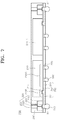
- FIG. 1 shows a cross-sectional view illustrating a stack package, according to an embodiment.
- FIGS. 2 to 6 illustrate a first sub-package included in the stack package of FIG. 1 .
- FIGS. 7 to 11 illustrate a second sub-package included in the stack package of FIG. 1 .
- FIGS. 12 to 14 illustrate a suppression effect of a void phenomenon in a stack package, according to an embodiment.
- FIG. 15 shows a cross-sectional view illustrating a bowing phenomenon of a general stack package, according to a comparative example.
- FIG. 16 shows a cross-sectional view illustrating a heat radiation effect of a stack package, according to according to an embodiment.
- FIG. 17 shows a block diagram illustrating an electronic system employing a memory card including a stack package, according to an embodiment.
- FIG. 18 shows a block diagram illustrating another electronic system including a stack package, according to an embodiment.
- spatially relative terms such as “beneath,” “below,” “lower,” “above,” “upper,” “top,” “bottom,” and the like, may be used to describe an element and/or a feature's relationship to another element(s) and/or feature(s) as, for example, illustrated in the figures. It will be understood that spatially relative terms are intended to encompass different orientations of a device in use and/or operation in addition to the orientation depicted in the figures. For example, when a device in the figures is turned over, elements described as below and/or beneath other elements or features would then be oriented above the other elements or features. The device may be otherwise oriented (rotated 90 degrees or at other orientations) and the spatially relative descriptors used herein interpreted accordingly.
- a semiconductor package may include electronic devices such as semiconductor chips or semiconductor dies.
- the semiconductor chips or the semiconductor dies may be obtained by separating a semiconductor substrate, such as a wafer, into a plurality of pieces using a die sawing process.
- the semiconductor chips may correspond to memory chips, logic chips (including application specific integrated circuits (ASIC) chips), or system-on-chips (SoC).
- ASIC application specific integrated circuits
- SoC system-on-chips
- the memory chips may include dynamic random access memory (DRAM) circuits, static random access memory (SRAM) circuits, NAND-type flash memory circuits, NOR-type flash memory circuits, magnetic random access memory (MRAM) circuits, resistive random access memory (ReRAM) circuits, ferroelectric random access memory (FeRAM) circuits, or phase change random access memory (PcRAM) circuits, which are integrated on the semiconductor substrate.
- DRAM dynamic random access memory
- SRAM static random access memory
- NAND-type flash memory circuits NAND-type flash memory circuits
- NOR-type flash memory circuits magnetic random access memory (MRAM) circuits
- resistive random access memory (ReRAM) circuits resistive random access memory (ReRAM) circuits
- FeRAM ferroelectric random access memory
- PcRAM phase change random access memory
- the logic chips may include logic circuits which are integrated on the semiconductor substrate.
- the semiconductor package may be employed in communication systems such as mobile phones, electronic systems associated with biotechnology or health care, or wearable electronic systems.
- FIG. 1 shows a cross-sectional view illustrating a stack package 10 , according to an embodiment.
- the stack package 10 may be configured to include a first sub-package 100 and a second sub-package 200 vertically stacked on the first sub-package 100 .
- Inner connectors 510 may be disposed between the first and second sub-packages 100 and 200 to electrically connect the first sub-packages 100 to the second sub-packages 200 .
- the inner connectors 510 may be connection members such as micro solder balls or conductive bumps.
- a plurality of dummy balls 550 may also be disposed between the first and second sub-packages 100 and 200 .
- the plurality of dummy balls 550 may be disposed to be spaced apart from and electrically isolated from the inner connectors 510 .
- the dummy balls 550 may be introduced to support the second sub-package 200 .
- Outer connectors 590 may be attached to the first sub-packages 100 to electrically connect with the first sub-packages 100 .
- the outer connectors 590 may be connection members for electrically connecting the stack package 10 to an external system or another electronic module.
- the outer connectors 590 may be solder balls.
- the stack package 10 may further include additional sub-packages vertically stacked on the second sub-stack package 200 .
- a third sub-package 300 may be vertically stacked on a surface of the second sub-stack package 200 opposite to the first sub-package 100
- a fourth sub-package 400 may be vertically stacked on a surface of the third sub-stack package 300 opposite to the second sub-package 200 .
- more sub-packages may be additionally stacked on a surface of the fourth sub-package 400 opposite to the third sub-package 300 .
- the inner connectors 510 and the dummy balls 550 may also be disposed between the second and third sub-packages 200 and 300 as well as between the third and fourth sub-packages 300 and 400 .
- each of the third and fourth sub-packages 300 and 400 may have the same shape and function as the second sub-package 200 .
- the stack package 10 may also include a filling layer 610 that fills a gap between the first and second sub-packages 100 and 200 .
- the filling layer 610 may include a dielectric layer for electrically isolating the second sub-package 200 from the first sub-package 100 .
- the filling layer 610 may include an underfill material.
- the filling layer 610 may be disposed to fill spaces between the second to fourth sub-packages 200 , 300 , and 400 .
- the filling layer 610 may extend to cover side surfaces of the second to fourth sub-packages 200 , 300 , and 400 .
- the stack package 10 may include an outer molding layer 650 that covers and protects the second to fourth sub-packages 200 , 300 , and 400 .
- the word “cover” can mean to directly cover or to indirectly cover.
- the outer molding layer 650 directly covers the fourth sub-package and indirectly covers the third sub-package.
- the outer molding layer 650 may be an encapsulating layer that covers a portion of the first sub-package 100 , the filling layer 610 , and the second to fourth sub-packages 200 , 300 , and 400 .
- the outer molding layer 650 may be formed on a surface of the first sub-package 100 using an encapsulant material such as an epoxy molding compound (EMC) material to cover the second to fourth sub-packages 200 , 300 , and 400 .
- EMC epoxy molding compound
- FIG. 1 illustrates an example in which the outer molding layer 650 is distinct from the filling layer 610
- the outer molding layer 650 and the filling layer 610 may be simultaneously formed using a molded underfill layer in some embodiments.
- FIG. 2 shows a cross-sectional view illustrating the first sub-package 100 included in the stack package 10 of FIG. 1 .
- FIG. 3 shows an enlarged view illustrating a portion (including a first bridge die 120 ) of the first sub-package 100 shown in FIG. 2 .
- FIG. 4 shows a plan view taken along a horizontal line Z 1 -Z 1 ′ of FIG. 3 to illustrate first redistributed lines 151 .
- FIG. 5 shows a plan view taken along a horizontal line Z 2 -Z 2 ′ of FIG. 3 to illustrate the first bridge die 120 and a first semiconductor die 110 .
- FIG. 6 shows a plan view taken along a horizontal line Z 3 -Z 3 ′ of FIG. 3 to illustrate first post bumps 125 and the first semiconductor die 110 .
- FIG. 2 corresponds to a cross-sectional view taken along a line X 1 -X 1 ′ of FIG. 4 .
- the first sub-package 100 may be provided as a single package unit disposed at a relatively low portion of the stack package 10 .
- the first sub-package 100 may be configured to include the first semiconductor die 110 and a first inner molding layer 160 covering and protecting the first semiconductor die 110 .
- the first semiconductor die 110 may be disposed on a first redistribution structure 150 .
- the first bridge die 120 may be disposed on the first redistribution structure 150 to be spaced apart from the first semiconductor die 110 .
- the first inner molding layer 160 may be formed to fill a gap between the first semiconductor die 110 and the first bridge die 120 , which are disposed on the first redistribution structure 150 .
- the first semiconductor die 110 may be disposed on the first redistribution structure 150 in a face-down shape such that a first surface 119 of the first semiconductor die 110 faces the first redistribution structure 150 .
- the first semiconductor die 110 may also include a second surface 118 which is located at opposite side of the first redistribution structure 150 and may further include side surfaces 117 extending from edges of the first surface 119 to edges of the second surface 118 .
- the first surface 119 of the first semiconductor die 110 may be an active surface at which integrated circuits of the first semiconductor die 110 are formed.
- the second surface 118 of the first semiconductor die 110 may be a bottom surface or a back side surface of the first semiconductor die 110 .
- the terms “first,” “second,” etc. in the first surface 119 and the second surface 118 are only used to distinguish one element from another element, are not used to define the element itself or to imply a particular sequence.
- First contact pads 111 may be disposed on the first surface 119 of the first semiconductor die 110 .
- the first contact pads 111 may act as conductive paths for electrically connecting the first semiconductor die 110 to an external device.
- the first contact pads 111 may correspond to edge pads which are disposed on both edge regions of the first semiconductor die 110 , as illustrated in a plan view of FIG. 5 .
- a third semiconductor die 110 - 1 may be disposed side by side with the first semiconductor die 110 on the first redistribution structure 150 .
- the third semiconductor die 110 - 1 may be a semiconductor die having substantially the same shape and configuration as the first semiconductor die 110 .
- the third semiconductor die 110 - 1 may be disposed to have a mirror image with respect to the first semiconductor die 110 .
- the first and third semiconductor dies 110 and 110 - 1 may be memory semiconductor dies, such as DRAM dies.
- the first bridge die 120 may be disposed to be spaced apart from one of the side surfaces 117 of the first semiconductor die 110 .
- the first bridge die 120 may be disposed on the first redistribution structure 150 such that one of side surfaces 127 of a body 129 of the first bridge die 120 faces one of the side surfaces 117 of the first semiconductor die 110 .
- the first bridge die 120 may be configured to include the body 129 and first post bumps 125 protruding from a top surface 128 of the body 129 . There may be a level difference H between the top surface 128 of the body 129 of the first bridge die 120 and the second surface 118 of the first semiconductor die 110 .
- the first bridge die 120 may be disposed to be adjacent to the first semiconductor die 110 such that the top surface 128 of the body 129 of the first bridge die 120 and the second surface 118 of the first semiconductor die 110 provide a step structure.
- the body 129 of the first bridge die 120 may be a semiconductor die having a thickness which is less than a thickness of the first semiconductor die 110 .
- the body 129 of the first bridge die 120 may have a thickness corresponding to 40% to 90% of a thickness of the first semiconductor die 110 .
- the body 129 of the first bridge die 120 may have a thickness corresponding to approximately 50% of a thickness of the first semiconductor die 110 .
- the first bridge die 120 may include first through vias 123 vertically penetrating the body 129 of the first bridge die 120 .
- the body 129 of the first bridge die 120 may include a semiconductor material such as a silicon material. Because the body 129 of the first bridge die 120 is made from a semiconductor material, the first through vias 123 may be formed using a semiconductor manufacturing process, for example, a silicon wafer-based manufacturing process. Thus, the first through vias 123 may be formed to have a through silicon via (TSV) structure with a fine diameter D 1 .
- TSV through silicon via
- the first through vias 123 may be formed of a conductive metal material, for example, a copper material.
- the first through vias 123 vertically penetrating the body 129 of the first bridge die 120 may have a length which is less than a thickness of the first semiconductor die 110 .
- the first through vias 123 vertically penetrating the body 129 of the first bridge die 120 may be formed to have a length corresponding to a thickness of the first semiconductor die 110 .
- the first through vias 123 vertically penetrating the body 129 of the first bridge die 120 may have a relatively short length as compared with a thickness of the first semiconductor die 110 .
- an aspect ratio of via holes in which the first through vias 123 are formed may be increased.
- a thickness of the body 129 of the first bridge die 120 increases, a length of the via holes penetrating the body 129 of the first bridge die 120 may increase and a diameter of the via holes may also increase. That is, it may be difficult to form the via holes having a relatively increased length with a relatively reduced diameter.
- the via holes to be filled with the first through vias 123 may have a relatively reduced length.
- the first through vias 123 may be formed to have the fine diameter D 1 . As a result, it may be possible to increase the number of the first through vias 123 formed in a limited area.
- the first post bumps 125 may be electrically connected to upper portions of the first through vias 123 , respectively.
- the first post bumps 125 may be disposed to overlap with the first through vias 123 in a plan view.
- overlap can mean partially overlapping for some embodiments and completely overlapping for other embodiments.
- the first post bumps 125 for example, completely overlap the first through vias 123 when the first through vias 123 are completely covered, either directly or indirectly, by the first post bumps 125 .
- the first post bumps 125 may protrude from the top surface 128 of the body 129 to have a certain height such that lower portions of side surfaces 125 S of the first post bumps 125 face an upper portion of the side surface 117 of the first semiconductor die 110 .
- the first inner molding layer 160 of the first sub-package 100 may be formed to cover the top surface 128 of the body 129 and to surround the side surfaces of the first post bumps 125 .
- the first inner molding layer 160 may be formed to directly cover the side surfaces of the first post bumps 125 and to expose top surfaces 125 T of the first post bumps 125 .
- a distance L 1 between a top surface 160 T of the first inner molding layer 160 and the top surface 128 of the body 129 may be greater than a distance L 2 between the top surface 160 T of the first inner molding layer 160 and the second surface 118 of the first semiconductor die 110 .
- the inner connectors 510 may be bonded to the top surfaces 125 T of the first post bumps 125 , as illustrated in FIG. 1 .
- the inner connectors 510 may electrically connect the first post bumps 125 to the second sub-package 200 .
- the first post bumps 125 may substantially penetrate a portion of the first inner molding layer 160 , which is located on the body 129 of the first bridge die 120 . Accordingly, the first post bumps 125 may extend electrical paths of the first through vias 123 to the top surface 160 T of the first inner molding layer 160 .
- the first inner molding layer 160 may include an insulation material.
- a space between the first through vias 123 may be filled with a semiconductor material, for example, a silicon material.
- a space between the first post bumps 125 may be filled with a dielectric material of the first inner molding layer 160 , for example, an epoxy molding compound (EMC) material. Since the first through vias 123 penetrate the body 129 made from a semiconductor material, an impedance value of each of the first through vias 123 may increase as compared with a case that the first through vias 123 penetrate a substrate including a dielectric material such as an EMC material.
- EMC epoxy molding compound
- a distance between the first through vias 123 may be reduced to more prominently cause signal noise such as crosstalk between the first through vias 123 .
- the signal noise between the first through vias 123 may affect a signal transmission characteristic or a signal integrity at a high frequency.
- a space between the first post bumps 125 is filled with a dielectric layer, such as an EMC material having a relatively low dielectric constant as compared with a semiconductor material, a crosstalk phenomenon between the first post bumps 125 may be more effectively suppressed.
- a silicon material may have a dielectric constant of approximately 11.68 and an EMC material may have a dielectric constant of approximately 3.7.
- the dielectric constant difference between the first inner molding layer 160 and the body 129 of the first bridge die 120 may influence an electrical characteristic of the first sub-package 100 .
- the first post bumps 125 may have a second diameter D 2 which is greater than the first diameter D 1 of the first through vias 123 . Because the first diameter D 1 corresponding to a diameter of the first through vias 123 is less than the second diameter D 2 corresponding to a diameter of first post bumps 125 , a distance between the first through vias 123 may be relatively greater than a distance between the first post bumps 125 . Accordingly, signal noises between the first through vias 123 may be efficiently suppressed.
- the first through vias 123 may serve to suppress generation of the signal noise between the first through vias 123 .
- the first diameter D 1 of the first through vias 123 may be reduced.
- a thickness of the body 129 of the first bridge die 120 may be reduced in order to obtain a fine diameter of the first through vias 123 .
- the first through vias 123 may be formed to have the first diameter D 1 corresponding to a fine diameter.
- a distance between the first through vias 123 may increase to suppress the generation of signal noise between the first through vias 123 .
- the first post bumps 125 may be metal post bumps including a copper material.
- the first post bumps 125 may have a vertical length or a height of approximately 60 micrometers, for some embodiments.
- the second diameter D 2 of the first post bumps 125 may be within the range of approximately 20 micrometers to approximately 30 micrometers, for some embodiments.
- the first diameter D 1 of the first through vias 123 may be approximately 0.5 micrometers, for some embodiments. Since the first post bumps 125 are formed to have the second diameter D 2 corresponding to a relatively large diameter, it may be possible to directly bond the inner connectors ( 510 of FIG. 1 ) such as solder balls or bumps to the top surfaces 125 T of the first post bumps 125 without misalignment. That is, the inner connectors ( 510 of FIG. 1 ) may be directly bonded to the top surfaces 125 T of the first post bumps 125 without using any additional conductive pads for increasing a contact area of the first post bumps 125 .
- the first inner molding layer 160 may be formed on a surface of the first redistribution structure 150 to cover the first bridge die 120 .
- the first inner molding layer 160 may have an extension part 160 E that extends laterally beyond side surfaces 200 S of the second sub-package 200 stacked on the first sub-package 100 , as illustrated in FIG. 1 . Since the first inner molding layer 160 of the first sub-package 100 has the extension part 160 E, the first sub-package 100 may have a width which is greater than a width of the second sub-package 200 stacked on the first sub-package 100 .
- the first redistribution structure 150 of the first sub-package 100 may be configured to include the first redistributed lines 151 and outer redistribution lines 155 for extending the first redistributed lines 151 .
- the first redistributed lines 151 and the outer redistribution lines 155 may be formed of a conductive layer including metal such as aluminum, copper, and gold.
- the first redistributed lines 151 may be conductive lines for electrically connecting the first bridge die 120 to the first semiconductor die 110 .
- the first redistribution structure 150 may include a first dielectric layer 152 revealing the first contact pads 111 of the first semiconductor die 110 and via pads 121 of the first bridge die 120 .
- the first redistributed lines 151 may be disposed on a surface of the first dielectric layer 152 opposite to the first bridge die 120 .
- Each of the first redistributed lines 151 may have a first overlap portion 151 D that vertically overlaps with and is electrically connected to any one of the first contact pads 111 revealed by the first dielectric layer 152 .
- Each of the first redistributed lines 151 may have a second overlap portion 151 B that vertically overlaps with and is electrically connected to any one of the via pads 121 revealed by the first dielectric layer 152 .
- Each of the first redistributed lines 151 may also include a connection portion 151 C extending from the first overlap portion 151 D to the second overlap portion 1518 .
- the via pads 121 of the first bridge die 120 may be disposed on a bottom surface of the body 129 of the first bridge die 120 to be located between the first through vias 123 and the second overlap portions 1518 of the first redistributed lines 151 . More specifically, the via pads 121 may be formed on bottom surfaces of the first through vias 123 for interconnection, and the second overlap portion 1518 of the first redistributed lines 151 may be formed to overlap with the via pads 121 .
- the via pads 121 may be connected to the first through vias 123 and may be formed to have a diameter which is greater than a diameter of the first through vias 123 .
- the via pads 121 may be interconnection members that electrically connect the first through vias 123 to the first redistributed lines 151 .
- the via pads 121 may be formed of a metal material such as a copper material or an aluminum material.
- the first redistribution structure 150 may further include a second dielectric layer 153 electrically isolating the first redistributed lines 151 from each other and revealing a portion of each of the first redistributed lines 151 .
- the outer redistribution lines 155 may be disposed on a bottom surface of the second dielectric layer 153 such that first ends of the outer redistribution lines 155 respectively overlap with the revealed portions of the first redistributed lines 151 .
- the outer redistribution lines 155 may be located at a different level from the first redistributed lines 151 .
- the first redistribution structure 150 may further include a third dielectric layer 154 electrically isolating the outer redistributed lines 155 from each other and revealing a portion of each of the outer redistributed lines 155 .
- the first to third dielectric layers 152 , 153 , and 154 may provide a dielectric structure that electrically isolates the first redistributed lines 151 and the outer redistributed lines 155 from each other.
- Portions 155 P of the outer redistributed lines 155 may be revealed by holes penetrating the third dielectric layer 154 , and the outer connectors 590 may be attached or bonded to the revealed portions 155 P of the outer redistributed lines 155 .
- the outer redistributed lines 155 may be introduced to extend electrical paths of the first redistributed lines 151 to the outer connectors 590 .
- FIG. 7 shows a cross-sectional view illustrating the second sub-package 200 included in the stack package 10 of FIG. 1 .
- FIG. 8 is an enlarged view illustrating a portion (including a second bridge die 220 ) of the second sub-package 200 shown in FIG. 7 .
- FIG. 9 shows a plan view taken along a horizontal line Z 4 -Z 4 ′ of FIG. 8 to illustrate second redistributed lines 251 .
- FIG. 10 shows a plan view taken along a horizontal line Z 5 -Z 5 ′ of FIG. 8 to illustrate the second bridge die 220 and a second semiconductor die 210 .
- FIG. 11 shows a plan view taken along a horizontal line Z 6 -Z 6 ′ of FIG. 8 to illustrate second post bumps 225 and the second semiconductor die 210 .
- FIG. 7 corresponds to a cross-sectional view taken along a line X 1 -X 1 ′ of FIG. 9 .
- the second sub-package 200 may be provided as a single package unit vertically stacked on the first sub-package 100 in the stack package 10 .
- the second sub-package 200 may include the second semiconductor die 210 and the second bridge die 220 , which are disposed on a second redistribution structure 250 to be spaced apart from each other.
- the second semiconductor die 210 may be a semiconductor die having a similar shape and a similar function to the first semiconductor die ( 110 of FIG. 1 ).
- the second semiconductor die 210 may be a memory semiconductor die having substantially the same shape and function as the first semiconductor die 110 .
- the second bridge die 220 may have substantially the same shape as the first bridge die 120 .
- the second semiconductor die 210 may be located to vertically overlap with the first semiconductor die 110
- the second bridge die 220 may be located to vertically overlap with the first bridge die 120 .
- the second sub-package 200 may be configured to include a second inner molding layer 260 that is disposed on the second redistribution structure 250 to cover and protect the second semiconductor die 210 and the second bridge die 220 .
- the second inner molding layer 260 may be substantially the same material as the first inner molding layer ( 160 of FIG. 1 ).
- the second inner molding layer 260 may be formed to fill a gap between the second semiconductor die 210 and the second bridge die 220 , which are disposed on the second redistribution structure 250 .
- the second inner molding layer 260 may be formed to have a width which is less than a width of the first inner molding layer 160 such that the extension part 160 E of the first inner molding layer 160 laterally protrudes from the side surfaces 200 S of the second sub-package 200 , as illustrated in FIG. 1 .
- second contact pads 211 may be disposed on a surface of the second semiconductor die 210 similar to the first contact pads 111 disposed on the first semiconductor die 110 .
- the second contact pads 211 may correspond to edge pads which are disposed on both edge regions of the second semiconductor die 210 , as illustrated in the plan view of FIG. 10 .
- a fourth semiconductor die 210 - 1 may be disposed side by side with the second semiconductor die 210 on the second redistribution structure 250 .
- the fourth semiconductor die 210 - 1 may be a semiconductor die having substantially the same shape and configuration as the second semiconductor die 210 .
- the fourth semiconductor die 210 - 1 may be disposed to have a mirror image with respect to the second semiconductor die 210 .
- the second and fourth semiconductor dies 210 and 210 - 1 may be memory semiconductor dies.
- the second bridge die 220 may be disposed to be spaced apart from the second semiconductor die 210 .
- the second bridge die 220 may be configured to include a body 229 and second post bumps 225 protruding from a top surface 228 of the body 229 .
- the second post bumps 225 may be electrically connected to upper portions of second through vias 223 vertically penetrating the body 229 , respectively.
- the second post bumps 225 may be disposed to overlap with the second through vias 223 in a plan view.
- the second inner molding layer 260 may be formed to cover the top surface 228 of the body 229 and to surround side surfaces of the second post bumps 225 .
- the second inner molding layer 260 may be formed to expose top surfaces 225 T of the second post bumps 225 .
- the second redistribution structure 250 of the second sub-package 200 may be configured to include the second redistributed lines 251 .
- the second redistributed lines 251 may be conductive lines for electrically connecting the second bridge die 220 to the second semiconductor die 210 .
- the second redistribution structure 250 may include a fourth dielectric layer 252 revealing the second contact pads 211 of the second semiconductor die 210 and via pads 221 of the second bridge die 220 .
- the via pads 221 of the second bridge die 220 may be disposed on a bottom surface of the body 229 of the second bridge die 220 to be located between the second through vias 223 and fourth overlap portions 2518 of the second redistributed lines 251 . More specifically, the via pads 221 may be formed on bottom surfaces of the second through vias 223 for interconnection, and the fourth overlap portion 251 B of the second redistributed lines 251 may be formed to overlap with the via pads 221 .
- the second redistributed lines 251 may be disposed on a surface of the fourth dielectric layer 252 opposite to the second bridge die 220 .
- Third overlap portions 251 D of the second redistributed lines 251 may be disposed to overlap with the second contact pads 211 revealed by the fourth dielectric layer 252 and may be electrically connected to the second contact pads 211 .
- the fourth overlap portion 251 B of the second redistributed lines 251 may be disposed to overlap with the via pads 221 revealed by the fourth dielectric layer 252 and may be electrically connected to the via pads 221 .
- Each of the second redistributed lines 251 may also include a connection portion 251 C extending from the third overlap portion 251 D to the fourth overlap portion 251 B.
- the second redistribution structure 250 may further include a fifth dielectric layer 253 electrically isolating the second redistributed lines 251 from each other and revealing a portion 251 P of each of the second redistributed lines 251 .
- the inner connectors 510 may be attached to or bonded to the revealed portions 251 P of the second redistributed lines 251 .
- the second post bumps 225 may respectively overlap with the second through vias 223 in a plan view, and the second through vias 223 may respectively overlap with the via pads 221 in a plan view.
- the via pads 221 may respectively overlap with the fourth overlap portion 251 B of the second redistributed lines 251 in a plan view, and the fourth overlap portion 251 B may respectively overlap with the inner connectors 510 in a plan view.
- the second post bumps 225 , the second through vias 223 , the via pads 221 , the fourth overlap portion 251 B of the second redistributed lines 251 , and the inner connectors 510 may provide a plurality of vertical electric paths. Thus, as illustrated in FIG.
- the third sub-package 300 may be electrically connected to the first sub-package 100 through the vertical paths including the second post bumps 225 , the second through vias 223 , the via pads 221 , the fourth overlap portion 251 B of the second redistributed lines 251 , and the inner connectors 510 .
- a plurality of dummy pads 270 may be disposed on a surface of the fourth dielectric layer 252 opposite to the second semiconductor die 210 to be spaced apart from the second redistributed lines 251 .
- the dummy pads 270 may be conductive pads which are electrically isolated from the second redistributed lines 251 and the second semiconductor die 210 .
- the dummy pads 270 may be electrically insulated from the second semiconductor die 210 by the fourth dielectric layer 252 .
- the dummy pads 270 may be bases to which dummy balls 550 are attached or bonded. While a metal layer is easily wetted with a solder material, a dielectric layer might not be readily wetted with a solder material.
- the dummy balls 550 are realized using solder balls, it may be difficult to stably attach the solder balls to the fifth dielectric layer 253 of the second sub-package 200 or the first inner molding layer ( 160 of FIG. 1 ) of the first sub-package ( 100 of FIG. 1 ).
- the dummy pads 270 may be disposed on the fourth dielectric layer 252 to stably bond the dummy balls 550 to the dummy pads 270 .
- the dummy pads 270 may be formed while the second redistributed lines 251 are formed using a copper plating process. Thus, the dummy pads 270 and the second redistributed lines 251 may be located at the same level.
- the fifth dielectric layer 253 may be formed to expose the dummy pads 270 to directly attach or bond the dummy balls 550 to the dummy pads 270 in a subsequent process.
- the dummy pads 270 may be wetted with first portions 551 of the dummy balls 550 to be bonded to the dummy pads 270 and the top surfaces 160 T of the first inner molding layer 160 may be in contact with second portions 552 of the dummy balls 550 opposite to the dummy pads 270 .
- the dummy balls 550 bonded to the dummy pads 270 may have a diameter which is less than a diameter of the inner connectors 510 .
- the inner connectors 510 may be bonded to the first post bumps 125 by wetting the first post bumps 125 with the inner connectors 510 .
- a height of the inner connectors 510 may be reduced as compared with an initial height of the inner connectors 510 . Since the first inner molding layer 160 is not substantially wetted with the dummy balls 550 , the dummy balls 550 may maintain their initial height even after the inner connectors 510 are bonded to the first post bumps 125 .
- an initial diameter of the dummy balls 550 may be less than an initial diameter of the inner connectors 510 .
- the diameters of the dummy balls 550 and the inner connectors 510 may be construed as parameters meaning heights thereof.
- the inner connectors 510 may be provided to have an initial diameter of approximately 30 micrometers, and the dummy balls 550 may be provided to have an initial diameter of approximately 20 micrometers.
- the dummy pads 270 may be disposed to overlap with the second semiconductor die 210 in a plan view.
- the second contact pads 211 of the second semiconductor die 210 may be disposed on both edge regions 210 E of the second semiconductor die 210 , as illustrated in FIGS. 7 and 8 . Because the second contact pads 211 correspond to edge pads, the dummy pads 270 may be arrayed on a central region 210 C of the second semiconductor die 210 .
- the dummy pads 270 and the dummy balls 550 may be disposed to overlap with the second semiconductor die 210 and the fourth semiconductor die 210 - 1 . As illustrated in FIGS. 7 and 8 , the dummy balls 550 may be disposed on the central region 210 C of the second semiconductor die 210 so as not to overlap with second contact pads 211 .
- FIG. 12 shows a cross-sectional view illustrating voids 610 V generated in a stack package 11 R according to a comparative example.
- FIG. 13 shows a schematic view illustrating a phenomenon of void 610 V formation.
- FIG. 14 shows a plan view illustrating suppression of a void in a stack package according to an embodiment.
- the stack package 11 R may be configured to include first to fourth sub-packages 100 R, 200 R, 300 R, and 400 R, which are sequentially stacked. If the first to fourth sub-packages 100 R, 200 R, 300 R, and 400 R are sequentially stacked without using the dummy balls ( 550 of FIG. 1 ), the voids 610 V may be formed during an underfill process for filling gaps between the first to fourth sub-packages 100 R, 200 R, 300 R, and 400 R with a filling layer 610 R.
- the voids 610 V may be formed in a vertical overlap region of first semiconductor dies 110 R included in the first sub-package 100 R and second semiconductor dies 210 R included in the second sub-package 200 R.
- the first sub-package 100 R and the second sub-package 200 R may be electrically coupled to each other by inner connectors 510 R that electrically connect a first bridge die 120 R included in the first sub-package 100 R to a second bridge die 220 R included in the second sub-package 200 R.
- the voids 610 V which are not filled with the filling layer 610 R, may be formed between the inner connectors 510 R disposed between the first semiconductor dies 110 R and the second semiconductor dies 210 R.
- a wide empty space may exist between the first sub-package 100 R and the second sub-package 200 R before the filling layer 610 R is formed.
- a flow rate of the underfill material 611 R may be different according to the regions. For example, if the flow rate of the underfill material 611 R is non-uniform, some spaces may be surrounded by the underfill material 611 R after the filling layer 610 R is formed. As a result, the voids 610 V may be formed.
- the dummy balls may prevent the voids 610 V from being formed.
- the dummy balls 550 may be uniformly arrayed in a space between the first sub-package 100 and the second sub-package 200 .
- a flow rate of the underfill material 611 may become uniform due to the presence of the dummy balls 550 . That is, the dummy balls 550 may induce a capillary effect, and the underfill material 611 may flow uniformly due to the capillary effect.
- the dummy balls 550 may prevent the voids ( 610 V of FIG. 12 ) from being formed in spaces between the sub-packages ( 100 , 200 , 300 , and 400 of FIG. 1 ) while the filling layer 610 is formed.
- FIG. 15 shows a cross-sectional view illustrating a bowing phenomenon of sub-packages included in a stack package 15 R, according to a comparative example.
- the stack package 15 R may be configured to include first to fourth sub-packages 105 R, 205 R, 305 R, and 405 R, which are sequentially stacked. If the first to fourth sub-packages 105 R, 205 R, 305 R, and 405 R are sequentially stacked without using the dummy balls ( 550 of FIG. 1 ), the second to fourth sub-packages 205 R, 305 R, and 405 R may bow to cause cracks of stack package 15 R. While an outer molding layer 655 R covering the second to fourth sub-packages 205 R, 305 R, and 405 R is formed, a molding process accompanied by pressure may be performed. In such a case, the second to fourth sub-packages 205 R, 305 R, and 405 R may bow due to the pressure applied to the stack package 15 R.
- the first to fourth sub-packages 105 R, 205 R, 305 R, and 405 R may be supported by inner connectors 555 R.
- the inner connectors 555 R may be located to vertically overlap with both edge regions of each of the second to fourth sub-packages 205 R, 305 R, and 405 R. That is, no inner connectors exist in vertical overlap regions of the first and second semiconductor dies 115 R and 215 R included in the first and second sub-packages 105 R and 205 R. Similarly, no inner connectors exist in vertical overlap regions of semiconductor dies included in the third and fourth sub-packages 305 R and 405 R.
- the pressure applied to the stack package 15 R during the molding process may be concentrated on central portions of the second to fourth sub-packages 205 R, 305 R, and 405 R to cause deformation (e.g., warpage) of the second to fourth sub-packages 205 R, 305 R, and 405 R. If the second to fourth sub-packages 205 R, 305 R, and 405 R severely warp, cracks may be formed in the central portions of the second to fourth sub-packages 205 R, 305 R, and 405 R.
- the dummy balls may suppress or mitigate the warpage and cracks of the sub-packages 200 , 300 , and 400 .
- the dummy balls 550 may be uniformly arrayed in spaces between the sub-packages 100 , 200 , 300 , and 400 .
- the dummy balls 550 may be disposed to support the central portions of the second to fourth sub-packages 200 , 300 , and 400 .
- the dummy balls 550 may suppress the warpage of the second to fourth sub-packages 200 , 300 , and 400 during the molding process.
- FIG. 16 shows a cross-sectional view illustrating an improved heat dissipation effect (also referred to as a heat radiation effect) of the stack package 10 shown in FIG. 1 .
- the dummy balls 550 may be introduced into spaces between the sub-packages 100 , 200 , 300 , and 400 of the stack package 10 .
- the dummy balls 550 may be formed of a material having a thermal conductivity which is higher than a thermal conductivity of the filling layer 610 .
- the dummy balls 550 may be formed of a metal material or a solder material. Because a thermal conductivity of the dummy balls 550 is higher than a thermal conductivity of the filling layer 610 , the dummy balls 550 may act as heat radiation paths (also referred to as heat dissipation paths) between the sub-packages 100 , 200 , 300 , and 400 .
- heat generated in the sub-packages 100 , 200 , 300 , and 400 may be more effectively radiated toward the top surface 650 T of the outer molding layer 650 through the dummy balls 550 .
- the dummy balls 550 may improve a heat dissipation characteristic of the stack package 10 .
- a heat spreader or a heat sink may be additionally attached to the top surface 650 T of the outer molding layer 650 to further improve heat dissipation.
- FIG. 17 shows a block diagram illustrating an electronic system including a memory card 7800 employing a stack package according to an embodiment.
- the memory card 7800 includes a memory 7810 , such as a nonvolatile memory device, and a memory controller 7820 .
- the memory 7810 and the memory controller 7820 may store data or read out the stored data.
- At least one of the memory 7810 and the memory controller 7820 may include the stack package according to an embodiment.
- the memory 7810 may include a nonvolatile memory device to which the technology of the embodiments of the present disclosure is applied.
- the memory controller 7820 may control the memory 7810 such that stored data is read out or data is stored in response to a read/write request from a host 7830 .
- FIG. 18 shows a block diagram illustrating an electronic system 8710 including the stack package, according to the embodiment.
- the electronic system 8710 may include a controller 8711 , an input/output device 8712 , and a memory 8713 .
- the controller 8711 , the input/output device 8712 , and the memory 8713 may be coupled with one another through a bus 8715 providing a path through which data move.
- the controller 8711 may include one or more microprocessors, digital signal processors, microcontrollers, and/or logic devices capable of performing the same functions as such components.
- the controller 8711 and/or the memory 8713 may include one or more stack packages according to embodiments of the present disclosure.
- the input/output device 8712 may include at least one selected among a keypad, a keyboard, a display device, a touchscreen, and so forth.
- the memory 8713 is a device for storing data.
- the memory 8713 may store data and/or commands to be executed by the controller 8711 , and the like.
- the memory 8713 may include a volatile memory device, such as a DRAM, and/or a nonvolatile memory device, such as a flash memory.
- a flash memory may be mounted to an information processing system, such as a mobile terminal or a desktop computer.
- the flash memory may constitute a solid state disk (SSD).
- SSD solid state disk
- the electronic system 8710 may stably store a large amount of data in a flash memory system.
- the electronic system 8710 may further include an interface 8714 configured to transmit and receive data to and from a communication network.
- the interface 8714 may be a wired or wireless type.
- the interface 8714 may include an antenna or a wired or wireless transceiver.
- the electronic system 8710 may be realized as a mobile system, a personal computer, an industrial computer, or a logic system performing various functions.
- the mobile system may be any one of a personal digital assistant (PDA), a portable computer, a tablet computer, a mobile phone, a smart phone, a wireless phone, a laptop computer, a memory card, a digital music system, and an information transmission/reception system.
- PDA personal digital assistant
- the electronic system 8710 may be used in a communication system using a technique of CDMA (code division multiple access), GSM (global system for mobile communications), NADC (north American digital cellular), E-TDMA (enhanced-time division multiple access), WCDAM (wideband code division multiple access), CDMA2000, LTE (long term evolution), or Wibro (wireless broadband Internet).
- CDMA code division multiple access
- GSM global system for mobile communications
- NADC node
- E-TDMA enhanced-time division multiple access
- WCDAM wideband code division multiple access
- CDMA2000 Code Division Multiple Access 2000
- LTE long term evolution
- Wibro wireless broadband Internet
Landscapes
- Engineering & Computer Science (AREA)
- Microelectronics & Electronic Packaging (AREA)
- Power Engineering (AREA)
- Computer Hardware Design (AREA)
- Physics & Mathematics (AREA)
- Condensed Matter Physics & Semiconductors (AREA)
- General Physics & Mathematics (AREA)
- Manufacturing & Machinery (AREA)
- Ceramic Engineering (AREA)
- Production Of Multi-Layered Print Wiring Board (AREA)
- Stacking Of Articles And Auxiliary Devices (AREA)
- Stackable Containers (AREA)
Applications Claiming Priority (2)
| Application Number | Priority Date | Filing Date | Title |
|---|---|---|---|
| KR1020180101256A KR102556517B1 (ko) | 2018-08-28 | 2018-08-28 | 브리지 다이를 포함하는 스택 패키지 |
| KR10-2018-0101256 | 2018-08-28 |
Publications (2)
| Publication Number | Publication Date |
|---|---|
| US20200075542A1 US20200075542A1 (en) | 2020-03-05 |
| US10658332B2 true US10658332B2 (en) | 2020-05-19 |
Family
ID=69640726
Family Applications (1)
| Application Number | Title | Priority Date | Filing Date |
|---|---|---|---|
| US16/219,676 Active US10658332B2 (en) | 2018-08-28 | 2018-12-13 | Stack packages including bridge dies |
Country Status (4)
| Country | Link |
|---|---|
| US (1) | US10658332B2 (ko) |
| KR (1) | KR102556517B1 (ko) |
| CN (1) | CN110867434A (ko) |
| TW (1) | TWI778197B (ko) |
Cited By (2)
| Publication number | Priority date | Publication date | Assignee | Title |
|---|---|---|---|---|
| US10971452B2 (en) * | 2019-09-06 | 2021-04-06 | SK Hynix Inc. | Semiconductor package including electromagnetic interference shielding layer |
| US12002786B2 (en) * | 2021-05-03 | 2024-06-04 | Samsung Electronics Co., Ltd. | Semiconductor package and method of fabricating the same |
Families Citing this family (7)
| Publication number | Priority date | Publication date | Assignee | Title |
|---|---|---|---|---|
| US9825007B1 (en) | 2016-07-13 | 2017-11-21 | Taiwan Semiconductor Manufacturing Co., Ltd. | Chip package structure with molding layer and method for forming the same |
| US11469215B2 (en) * | 2016-07-13 | 2022-10-11 | Taiwan Semiconductor Manufacturing Co., Ltd. | Chip package structure with molding layer and method for forming the same |
| US11309226B2 (en) * | 2019-12-18 | 2022-04-19 | Taiwan Semiconductor Manufacturing Company, Ltd. | Three-dimensional integrated circuit structures and methods of forming the same |
| US11239217B2 (en) * | 2020-03-30 | 2022-02-01 | Nanya Technology Corporation | Semiconductor package including a first sub-package stacked atop a second sub-package |
| KR20220028741A (ko) * | 2020-08-31 | 2022-03-08 | 에스케이하이닉스 주식회사 | 적층 반도체 칩을 포함하는 반도체 패키지 |
| US11658158B2 (en) | 2020-09-03 | 2023-05-23 | Taiwan Semiconductor Manufacturing Company Ltd. | Die to die interface circuit |
| TWI786698B (zh) * | 2021-06-25 | 2022-12-11 | 力晶積成電子製造股份有限公司 | 半導體封裝 |
Citations (3)
| Publication number | Priority date | Publication date | Assignee | Title |
|---|---|---|---|---|
| US20100171208A1 (en) * | 2009-01-06 | 2010-07-08 | Elpida Memory, Inc. | Semiconductor device |
| KR101236798B1 (ko) | 2011-02-16 | 2013-02-25 | 앰코 테크놀로지 코리아 주식회사 | 웨이퍼 레벨 적층형 반도체 패키지 제조 방법 |
| KR20160023481A (ko) | 2014-08-22 | 2016-03-03 | 삼성전자주식회사 | 칩 적층 반도체 패키지 |
Family Cites Families (16)
| Publication number | Priority date | Publication date | Assignee | Title |
|---|---|---|---|---|
| US7550857B1 (en) * | 2006-11-16 | 2009-06-23 | Amkor Technology, Inc. | Stacked redistribution layer (RDL) die assembly package |
| US8035235B2 (en) * | 2009-09-15 | 2011-10-11 | Stats Chippac Ltd. | Integrated circuit packaging system with package-on-package and method of manufacture thereof |
| US8115293B2 (en) * | 2009-12-08 | 2012-02-14 | Stats Chippac Ltd. | Integrated circuit packaging system with interconnect and method of manufacture thereof |
| KR101719636B1 (ko) * | 2011-01-28 | 2017-04-05 | 삼성전자 주식회사 | 반도체 장치 및 그 제조 방법 |
| JP2013183120A (ja) * | 2012-03-05 | 2013-09-12 | Elpida Memory Inc | 半導体装置 |
| DE112013002672T5 (de) * | 2012-05-25 | 2015-03-19 | Nepes Co., Ltd | Halbleitergehäuse, Verfahren zum Herstellen desselben und Gehäuse auf Gehäuse |
| KR101368793B1 (ko) * | 2012-05-25 | 2014-03-03 | 주식회사 네패스 | 반도체 패키지 및 그 제조 방법 |
| KR102190382B1 (ko) * | 2012-12-20 | 2020-12-11 | 삼성전자주식회사 | 반도체 패키지 |
| KR20150025939A (ko) * | 2013-08-30 | 2015-03-11 | 삼성전기주식회사 | 인터포저 및 이를 이용한 반도체 패키지, 그리고 인터포저의 제조 방법 |
| US9825009B2 (en) * | 2015-09-03 | 2017-11-21 | Bridge Semiconductor Corporation | Interconnect substrate having cavity for stackable semiconductor assembly, manufacturing method thereof and vertically stacked semiconductor assembly using the same |
| US20160365334A1 (en) * | 2015-06-09 | 2016-12-15 | Inotera Memories, Inc. | Package-on-package assembly and method for manufacturing the same |
| KR102413441B1 (ko) * | 2015-11-12 | 2022-06-28 | 삼성전자주식회사 | 반도체 패키지 |
| KR102579876B1 (ko) * | 2016-02-22 | 2023-09-18 | 삼성전자주식회사 | 반도체 패키지 |
| US10276548B2 (en) * | 2016-09-14 | 2019-04-30 | Taiwan Semiconductor Manufacturing Company, Ltd. | Semiconductor packages having dummy connectors and methods of forming same |
| US10529697B2 (en) * | 2016-09-16 | 2020-01-07 | Taiwan Semiconductor Manufacturing Company, Ltd. | Package structure and method of forming the same |
| KR102517464B1 (ko) * | 2018-04-30 | 2023-04-04 | 에스케이하이닉스 주식회사 | 반도체 다이와 이격된 브리지 다이를 포함하는 반도체 패키지 |
-
2018
- 2018-08-28 KR KR1020180101256A patent/KR102556517B1/ko active IP Right Grant
- 2018-12-12 CN CN201811515828.5A patent/CN110867434A/zh active Pending
- 2018-12-13 US US16/219,676 patent/US10658332B2/en active Active
- 2018-12-19 TW TW107145890A patent/TWI778197B/zh active
Patent Citations (4)
| Publication number | Priority date | Publication date | Assignee | Title |
|---|---|---|---|---|
| US20100171208A1 (en) * | 2009-01-06 | 2010-07-08 | Elpida Memory, Inc. | Semiconductor device |
| US8304877B2 (en) | 2009-01-06 | 2012-11-06 | Elpida Memory, Inc. | Semiconductor device |
| KR101236798B1 (ko) | 2011-02-16 | 2013-02-25 | 앰코 테크놀로지 코리아 주식회사 | 웨이퍼 레벨 적층형 반도체 패키지 제조 방법 |
| KR20160023481A (ko) | 2014-08-22 | 2016-03-03 | 삼성전자주식회사 | 칩 적층 반도체 패키지 |
Cited By (2)
| Publication number | Priority date | Publication date | Assignee | Title |
|---|---|---|---|---|
| US10971452B2 (en) * | 2019-09-06 | 2021-04-06 | SK Hynix Inc. | Semiconductor package including electromagnetic interference shielding layer |
| US12002786B2 (en) * | 2021-05-03 | 2024-06-04 | Samsung Electronics Co., Ltd. | Semiconductor package and method of fabricating the same |
Also Published As
| Publication number | Publication date |
|---|---|
| TWI778197B (zh) | 2022-09-21 |
| TW202010085A (zh) | 2020-03-01 |
| KR20200024499A (ko) | 2020-03-09 |
| CN110867434A (zh) | 2020-03-06 |
| KR102556517B1 (ko) | 2023-07-18 |
| US20200075542A1 (en) | 2020-03-05 |
Similar Documents
| Publication | Publication Date | Title |
|---|---|---|
| US10658332B2 (en) | Stack packages including bridge dies | |
| US10991640B2 (en) | Semiconductor packages including bridge die | |
| US10985106B2 (en) | Stack packages including bridge dies | |
| US9570370B2 (en) | Multi chip package and method for manufacturing the same | |
| US9153557B2 (en) | Chip stack embedded packages | |
| US11322446B2 (en) | System-in-packages including a bridge die | |
| US20150311182A1 (en) | Semiconductor package and method for manufacturing the same | |
| US20200273799A1 (en) | System-in-packages including a bridge die | |
| US10903131B2 (en) | Semiconductor packages including bridge die spaced apart from semiconductor die | |
| US11495545B2 (en) | Semiconductor package including a bridge die | |
| US11201140B2 (en) | Semiconductor packages including stacked sub-packages with interposing bridges | |
| US20180286835A1 (en) | Semiconductor packages and methods of manufacturing the same | |
| US10903196B2 (en) | Semiconductor packages including bridge die | |
| US11127687B2 (en) | Semiconductor packages including modules stacked with interposing bridges | |
| US10361141B2 (en) | Semiconductor packages relating to thermal transfer plate and methods of manufacturing the same | |
| US11233033B2 (en) | Semiconductor packages including chips stacked on a base module | |
| US11152335B2 (en) | Stack packages including a supporting substrate | |
| US20230317683A1 (en) | Semiconductor package including heat dissipation layer | |
| US10998294B2 (en) | Semiconductor packages having stacked chip structure | |
| US20230120361A1 (en) | Semiconductor devices including substrates bonded to each other and methods for fabricating the same | |
| US20200328189A1 (en) | Semiconductor packages including a thermal conduction network structure | |
| CN111613601B (zh) | 包括桥接晶片的半导体封装件 | |
| TWI836000B (zh) | 包括橋接晶粒的半導體封裝件 |
Legal Events
| Date | Code | Title | Description |
|---|---|---|---|
| AS | Assignment |
Owner name: SK HYNIX INC., KOREA, REPUBLIC OF Free format text: ASSIGNMENT OF ASSIGNORS INTEREST;ASSIGNORS:SUNG, KI JUN;KIM, JONG HOON;REEL/FRAME:047772/0244 Effective date: 20181203 |
|
| FEPP | Fee payment procedure |
Free format text: ENTITY STATUS SET TO UNDISCOUNTED (ORIGINAL EVENT CODE: BIG.); ENTITY STATUS OF PATENT OWNER: LARGE ENTITY |
|
| STPP | Information on status: patent application and granting procedure in general |
Free format text: PUBLICATIONS -- ISSUE FEE PAYMENT VERIFIED |
|
| STCF | Information on status: patent grant |
Free format text: PATENTED CASE |
|
| MAFP | Maintenance fee payment |
Free format text: PAYMENT OF MAINTENANCE FEE, 4TH YEAR, LARGE ENTITY (ORIGINAL EVENT CODE: M1551); ENTITY STATUS OF PATENT OWNER: LARGE ENTITY Year of fee payment: 4 |