US10586898B2 - Method of manufacturing light emitting device - Google Patents
Method of manufacturing light emitting device Download PDFInfo
- Publication number
- US10586898B2 US10586898B2 US16/146,521 US201816146521A US10586898B2 US 10586898 B2 US10586898 B2 US 10586898B2 US 201816146521 A US201816146521 A US 201816146521A US 10586898 B2 US10586898 B2 US 10586898B2
- Authority
- US
- United States
- Prior art keywords
- light emitting
- light
- resin
- transmissive
- alignment mark
- Prior art date
- Legal status (The legal status is an assumption and is not a legal conclusion. Google has not performed a legal analysis and makes no representation as to the accuracy of the status listed.)
- Active
Links
- 238000004519 manufacturing process Methods 0.000 title claims abstract description 52
- 229920005989 resin Polymers 0.000 claims abstract description 142
- 239000011347 resin Substances 0.000 claims abstract description 142
- 238000005520 cutting process Methods 0.000 claims abstract description 40
- 238000000034 method Methods 0.000 claims abstract description 8
- 238000006243 chemical reaction Methods 0.000 claims description 12
- 239000000126 substance Substances 0.000 claims description 12
- 238000000748 compression moulding Methods 0.000 claims description 5
- 238000000227 grinding Methods 0.000 claims description 4
- 229910052751 metal Inorganic materials 0.000 description 26
- 239000002184 metal Substances 0.000 description 26
- 230000015572 biosynthetic process Effects 0.000 description 23
- 239000000758 substrate Substances 0.000 description 14
- 239000004065 semiconductor Substances 0.000 description 7
- 238000000206 photolithography Methods 0.000 description 6
- 239000000463 material Substances 0.000 description 5
- XLYOFNOQVPJJNP-UHFFFAOYSA-N water Substances O XLYOFNOQVPJJNP-UHFFFAOYSA-N 0.000 description 4
- 230000018109 developmental process Effects 0.000 description 3
- 238000002845 discoloration Methods 0.000 description 3
- 239000000945 filler Substances 0.000 description 3
- 239000007788 liquid Substances 0.000 description 3
- 229920002050 silicone resin Polymers 0.000 description 3
- 239000000853 adhesive Substances 0.000 description 2
- 230000001070 adhesive effect Effects 0.000 description 2
- 238000009837 dry grinding Methods 0.000 description 2
- 230000000694 effects Effects 0.000 description 2
- 239000003822 epoxy resin Substances 0.000 description 2
- 238000005530 etching Methods 0.000 description 2
- 230000012447 hatching Effects 0.000 description 2
- 230000001678 irradiating effect Effects 0.000 description 2
- 229920000647 polyepoxide Polymers 0.000 description 2
- 238000005507 spraying Methods 0.000 description 2
- 238000003756 stirring Methods 0.000 description 2
- 238000001721 transfer moulding Methods 0.000 description 2
- RGYAVZGBAJFMIZ-UHFFFAOYSA-N 2,3-dimethylhex-2-ene Chemical compound CCCC(C)=C(C)C RGYAVZGBAJFMIZ-UHFFFAOYSA-N 0.000 description 1
- 239000004925 Acrylic resin Substances 0.000 description 1
- 229920000178 Acrylic resin Polymers 0.000 description 1
- CURLTUGMZLYLDI-UHFFFAOYSA-N Carbon dioxide Chemical compound O=C=O CURLTUGMZLYLDI-UHFFFAOYSA-N 0.000 description 1
- RYGMFSIKBFXOCR-UHFFFAOYSA-N Copper Chemical compound [Cu] RYGMFSIKBFXOCR-UHFFFAOYSA-N 0.000 description 1
- GWEVSGVZZGPLCZ-UHFFFAOYSA-N Titan oxide Chemical compound O=[Ti]=O GWEVSGVZZGPLCZ-UHFFFAOYSA-N 0.000 description 1
- 238000005422 blasting Methods 0.000 description 1
- 235000011089 carbon dioxide Nutrition 0.000 description 1
- 229910052802 copper Inorganic materials 0.000 description 1
- 239000010949 copper Substances 0.000 description 1
- 238000009713 electroplating Methods 0.000 description 1
- 238000000605 extraction Methods 0.000 description 1
- 239000006260 foam Substances 0.000 description 1
- 238000010438 heat treatment Methods 0.000 description 1
- 238000000465 moulding Methods 0.000 description 1
- 239000005011 phenolic resin Substances 0.000 description 1
- 229920000636 poly(norbornene) polymer Polymers 0.000 description 1
- 229920005668 polycarbonate resin Polymers 0.000 description 1
- 239000004431 polycarbonate resin Substances 0.000 description 1
- 239000002002 slurry Substances 0.000 description 1
- 229910000679 solder Inorganic materials 0.000 description 1
- OGIDPMRJRNCKJF-UHFFFAOYSA-N titanium oxide Inorganic materials [Ti]=O OGIDPMRJRNCKJF-UHFFFAOYSA-N 0.000 description 1
- 239000012463 white pigment Substances 0.000 description 1
Images


Classifications
-
- H—ELECTRICITY
- H01—ELECTRIC ELEMENTS
- H01L—SEMICONDUCTOR DEVICES NOT COVERED BY CLASS H10
- H01L33/00—Semiconductor devices having potential barriers specially adapted for light emission; Processes or apparatus specially adapted for the manufacture or treatment thereof or of parts thereof; Details thereof
- H01L33/48—Semiconductor devices having potential barriers specially adapted for light emission; Processes or apparatus specially adapted for the manufacture or treatment thereof or of parts thereof; Details thereof characterised by the semiconductor body packages
- H01L33/52—Encapsulations
- H01L33/56—Materials, e.g. epoxy or silicone resin
-
- H—ELECTRICITY
- H01—ELECTRIC ELEMENTS
- H01L—SEMICONDUCTOR DEVICES NOT COVERED BY CLASS H10
- H01L21/00—Processes or apparatus adapted for the manufacture or treatment of semiconductor or solid state devices or of parts thereof
- H01L21/70—Manufacture or treatment of devices consisting of a plurality of solid state components formed in or on a common substrate or of parts thereof; Manufacture of integrated circuit devices or of parts thereof
- H01L21/77—Manufacture or treatment of devices consisting of a plurality of solid state components or integrated circuits formed in, or on, a common substrate
- H01L21/78—Manufacture or treatment of devices consisting of a plurality of solid state components or integrated circuits formed in, or on, a common substrate with subsequent division of the substrate into plural individual devices
-
- H—ELECTRICITY
- H01—ELECTRIC ELEMENTS
- H01L—SEMICONDUCTOR DEVICES NOT COVERED BY CLASS H10
- H01L23/00—Details of semiconductor or other solid state devices
- H01L23/544—Marks applied to semiconductor devices or parts, e.g. registration marks, alignment structures, wafer maps
-
- H—ELECTRICITY
- H01—ELECTRIC ELEMENTS
- H01L—SEMICONDUCTOR DEVICES NOT COVERED BY CLASS H10
- H01L33/00—Semiconductor devices having potential barriers specially adapted for light emission; Processes or apparatus specially adapted for the manufacture or treatment thereof or of parts thereof; Details thereof
- H01L33/005—Processes
- H01L33/0095—Post-treatment of devices, e.g. annealing, recrystallisation or short-circuit elimination
-
- H—ELECTRICITY
- H01—ELECTRIC ELEMENTS
- H01L—SEMICONDUCTOR DEVICES NOT COVERED BY CLASS H10
- H01L33/00—Semiconductor devices having potential barriers specially adapted for light emission; Processes or apparatus specially adapted for the manufacture or treatment thereof or of parts thereof; Details thereof
- H01L33/48—Semiconductor devices having potential barriers specially adapted for light emission; Processes or apparatus specially adapted for the manufacture or treatment thereof or of parts thereof; Details thereof characterised by the semiconductor body packages
- H01L33/50—Wavelength conversion elements
- H01L33/507—Wavelength conversion elements the elements being in intimate contact with parts other than the semiconductor body or integrated with parts other than the semiconductor body
-
- H—ELECTRICITY
- H01—ELECTRIC ELEMENTS
- H01L—SEMICONDUCTOR DEVICES NOT COVERED BY CLASS H10
- H01L33/00—Semiconductor devices having potential barriers specially adapted for light emission; Processes or apparatus specially adapted for the manufacture or treatment thereof or of parts thereof; Details thereof
- H01L33/48—Semiconductor devices having potential barriers specially adapted for light emission; Processes or apparatus specially adapted for the manufacture or treatment thereof or of parts thereof; Details thereof characterised by the semiconductor body packages
- H01L33/62—Arrangements for conducting electric current to or from the semiconductor body, e.g. lead-frames, wire-bonds or solder balls
-
- H—ELECTRICITY
- H01—ELECTRIC ELEMENTS
- H01L—SEMICONDUCTOR DEVICES NOT COVERED BY CLASS H10
- H01L2224/00—Indexing scheme for arrangements for connecting or disconnecting semiconductor or solid-state bodies and methods related thereto as covered by H01L24/00
- H01L2224/01—Means for bonding being attached to, or being formed on, the surface to be connected, e.g. chip-to-package, die-attach, "first-level" interconnects; Manufacturing methods related thereto
- H01L2224/10—Bump connectors; Manufacturing methods related thereto
- H01L2224/15—Structure, shape, material or disposition of the bump connectors after the connecting process
- H01L2224/16—Structure, shape, material or disposition of the bump connectors after the connecting process of an individual bump connector
- H01L2224/161—Disposition
- H01L2224/16151—Disposition the bump connector connecting between a semiconductor or solid-state body and an item not being a semiconductor or solid-state body, e.g. chip-to-substrate, chip-to-passive
- H01L2224/16221—Disposition the bump connector connecting between a semiconductor or solid-state body and an item not being a semiconductor or solid-state body, e.g. chip-to-substrate, chip-to-passive the body and the item being stacked
- H01L2224/16225—Disposition the bump connector connecting between a semiconductor or solid-state body and an item not being a semiconductor or solid-state body, e.g. chip-to-substrate, chip-to-passive the body and the item being stacked the item being non-metallic, e.g. insulating substrate with or without metallisation
-
- H—ELECTRICITY
- H01—ELECTRIC ELEMENTS
- H01L—SEMICONDUCTOR DEVICES NOT COVERED BY CLASS H10
- H01L2224/00—Indexing scheme for arrangements for connecting or disconnecting semiconductor or solid-state bodies and methods related thereto as covered by H01L24/00
- H01L2224/73—Means for bonding being of different types provided for in two or more of groups H01L2224/10, H01L2224/18, H01L2224/26, H01L2224/34, H01L2224/42, H01L2224/50, H01L2224/63, H01L2224/71
- H01L2224/732—Location after the connecting process
- H01L2224/73251—Location after the connecting process on different surfaces
- H01L2224/73253—Bump and layer connectors
-
- H—ELECTRICITY
- H01—ELECTRIC ELEMENTS
- H01L—SEMICONDUCTOR DEVICES NOT COVERED BY CLASS H10
- H01L2933/00—Details relating to devices covered by the group H01L33/00 but not provided for in its subgroups
- H01L2933/0008—Processes
- H01L2933/0033—Processes relating to semiconductor body packages
-
- H—ELECTRICITY
- H01—ELECTRIC ELEMENTS
- H01L—SEMICONDUCTOR DEVICES NOT COVERED BY CLASS H10
- H01L2933/00—Details relating to devices covered by the group H01L33/00 but not provided for in its subgroups
- H01L2933/0008—Processes
- H01L2933/0033—Processes relating to semiconductor body packages
- H01L2933/0041—Processes relating to semiconductor body packages relating to wavelength conversion elements
-
- H—ELECTRICITY
- H01—ELECTRIC ELEMENTS
- H01L—SEMICONDUCTOR DEVICES NOT COVERED BY CLASS H10
- H01L2933/00—Details relating to devices covered by the group H01L33/00 but not provided for in its subgroups
- H01L2933/0008—Processes
- H01L2933/0033—Processes relating to semiconductor body packages
- H01L2933/0058—Processes relating to semiconductor body packages relating to optical field-shaping elements
-
- H—ELECTRICITY
- H01—ELECTRIC ELEMENTS
- H01L—SEMICONDUCTOR DEVICES NOT COVERED BY CLASS H10
- H01L2933/00—Details relating to devices covered by the group H01L33/00 but not provided for in its subgroups
- H01L2933/0008—Processes
- H01L2933/0033—Processes relating to semiconductor body packages
- H01L2933/0066—Processes relating to semiconductor body packages relating to arrangements for conducting electric current to or from the semiconductor body
-
- H—ELECTRICITY
- H01—ELECTRIC ELEMENTS
- H01L—SEMICONDUCTOR DEVICES NOT COVERED BY CLASS H10
- H01L33/00—Semiconductor devices having potential barriers specially adapted for light emission; Processes or apparatus specially adapted for the manufacture or treatment thereof or of parts thereof; Details thereof
- H01L33/48—Semiconductor devices having potential barriers specially adapted for light emission; Processes or apparatus specially adapted for the manufacture or treatment thereof or of parts thereof; Details thereof characterised by the semiconductor body packages
- H01L33/483—Containers
- H01L33/486—Containers adapted for surface mounting
-
- H—ELECTRICITY
- H01—ELECTRIC ELEMENTS
- H01L—SEMICONDUCTOR DEVICES NOT COVERED BY CLASS H10
- H01L33/00—Semiconductor devices having potential barriers specially adapted for light emission; Processes or apparatus specially adapted for the manufacture or treatment thereof or of parts thereof; Details thereof
- H01L33/48—Semiconductor devices having potential barriers specially adapted for light emission; Processes or apparatus specially adapted for the manufacture or treatment thereof or of parts thereof; Details thereof characterised by the semiconductor body packages
- H01L33/50—Wavelength conversion elements
- H01L33/501—Wavelength conversion elements characterised by the materials, e.g. binder
- H01L33/502—Wavelength conversion materials
-
- H—ELECTRICITY
- H01—ELECTRIC ELEMENTS
- H01L—SEMICONDUCTOR DEVICES NOT COVERED BY CLASS H10
- H01L33/00—Semiconductor devices having potential barriers specially adapted for light emission; Processes or apparatus specially adapted for the manufacture or treatment thereof or of parts thereof; Details thereof
- H01L33/48—Semiconductor devices having potential barriers specially adapted for light emission; Processes or apparatus specially adapted for the manufacture or treatment thereof or of parts thereof; Details thereof characterised by the semiconductor body packages
- H01L33/58—Optical field-shaping elements
- H01L33/60—Reflective elements
Definitions
- the present disclosure relates to a method of manufacturing a light emitting device.
- JP 2017-076719 A describes that a plurality of light emitting elements are mounted on a base member, a plurality of the mounted light emitting elements are covered with a resin sheet, the resin sheet is softened to fill gaps between the light emitting elements, and the base member and the resin sheet are cut at portions between the light emitting elements, to manufacture light emitting devices.
- One object of the present invention is to provide a method of manufacturing a light emitting device, having a reduced size, reduced weight, reduced cost, and with which the position of an alignment mark can be accurately recognized at the time of cutting to allow cutting into individual light emitting devices.
- a method of manufacturing a light emitting device in which a plurality of light emitting devices each including a light emitting element is formed collectively, and then separated into individual light emitting devices including, a base member providing step of providing a base member including: a wiring electrode to be connected to the light emitting elements, and an alignment mark, the wiring electrode and the alignment mark disposed on an upper surface of the base member; a mounting step of mounting each of the light emitting elements at a predetermined position; an alignment mark covering step of covering the alignment mark with a light-transmissive resin; a reflective resin forming step of forming a reflective resin surrounding the light emitting element so as to expose at least a part of a surface of the light-transmissive resin, the reflective resin reflecting light from the light emitting element; and a cutting step of recognizing the alignment mark through the exposed surface of the light-transmissive resin, and cutting the reflective resin and the base member with reference to the alignment mark to perform singulation into individual light emitting devices.
- the position of an alignment mark can be accurately recognized at the time of cutting to perform cutting into individual light emitting devices.
- Light emitting devices according to embodiments of the present invention can have a reduced size and reduced weight, and can be provided at a lower cost.
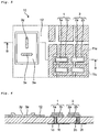
- FIG. 1 is a perspective view of a light emitting device manufactured using a method of manufacturing a light emitting device according to a first embodiment.
- FIG. 2 is a schematic cross-sectional view taken along line A-A in FIG. 1 .
- FIG. 3 is a schematic plan view showing an overall configuration of a base member used in a method of manufacturing a light emitting device according to the first embodiment.
- FIG. 4A is a schematic plan view of a unit alignment-mark formation region and FIG. 4B is a schematic plan view of a unit alignment-mark formation region.
- FIG. 5 is a schematic enlarged plan view of region C in FIG. 3 .
- FIG. 6 is a schematic cross-sectional view taken along a line B-B in FIG. 5 .
- FIG. 7A is a schematic cross-sectional view where a light emitting element is flip-chip-mounted on a base member.
- FIG. 7B is a schematic cross-sectional view where a light-transmissive member is bonded onto a light emitting element.
- FIG. 7C is a schematic cross-sectional view where a light-transmissive resin is applied to an alignment-mark formation region and cured.
- FIG. 7D is a schematic cross-sectional view where a reflective resin covering a light emitting element, a light-transmissive member and a light-transmissive resin is formed on a base member.
- FIG. 7E is a schematic cross-sectional view where a reflective resin is partially removed to expose an upper surface of a light-transmissive member and a surface of a light-transmissive resin.
- FIG. 7F is a schematic cross-sectional view showing a state in which the base member and a reflective resin are cut by a cutting blade.
- FIG. 7G is a schematic cross-sectional view where division into individual light emitting devices is performed.
- FIG. 8A is a schematic cross-sectional view where a wiring metal film is formed on a substrate in a base member providing step in a method of manufacturing according to the first embodiment.
- FIG. 8B is a schematic cross-sectional view where a first resist is formed on a wiring metal film in a base member providing step in the method of manufacturing according to the first embodiment.
- FIG. 8C is a schematic cross-sectional view where a first resist is exposed and developed in a base member providing step in the method of manufacturing according to the first embodiment.
- FIG. 8D is a schematic cross-sectional view where a wiring metal film is etched with a developed first resist as a mask in a base member providing step in the method of manufacturing according to the first embodiment.
- FIG. 8E is a schematic cross-sectional view where the first resist is removed after a wiring metal film is etched in a base member providing step in the method of manufacturing according to the first embodiment.
- FIG. 8F is a schematic cross-sectional view where a projection metal film is formed on a substrate including a first lower electrode, a second lower electrode and a wiring electrode in a base member providing step in method of manufacturing according to the first embodiment.
- FIG. 8G is a schematic cross-sectional view where a second resist is formed on a projection metal film in a base member providing step in the method of manufacturing according to the first embodiment.
- FIG. 8H is a schematic cross-sectional view where a second resist is exposed and developed in a base member providing step in the method of manufacturing according to the embodiment.
- FIG. 8I is a schematic cross-sectional view where a second resist is removed by etching a projection metal film with the second resist as a mask in a base member providing step in the method of manufacturing according to the embodiment.
- FIG. 1 is a perspective view of a light emitting device 100 manufactured using a method of manufacturing a light emitting device according to a first embodiment.
- FIG. 2 is a schematic cross-sectional view taken along line A-A in FIG. 1 .
- the light emitting device 100 includes a base member (hereinafter, may be referred to as a “singulated base member” because it is a base member after singulation) 101 , a light emitting element 30 , a light-transmissive member 50 and a reflective resin 70 .
- the singulated base member 101 has a first land electrode 1 and a second land electrode 2 that are disposed on an upper surface of the singulated member 101 , and a first terminal electrode 1 t and a second terminal electrode 2 t that are disposed on a lower surface of the singulated member 101 .
- the first land electrode 1 includes a first lower electrode 1 b , and a first projection 1 a on the first lower electrode 1 b .
- the second land electrode 2 includes a second lower electrode 2 b , a second projection 2 a on the second lower electrode 2 b .
- the first land electrode 1 is connected to the first terminal electrode 1 t by a connection electrode 1 c disposed on a lateral surface that defines a through-hole extending through the singulated base member 101 and provided directly below the first land electrode 1 .
- the second land electrode 2 is connected to the second terminal electrode 2 t by a connection electrode 2 c disposed on a lateral surface of a through-hole extending through the singulated base member 101 and provided directly below the second land electrode 2 .
- Each of the connection electrodes 1 c and 2 c is disposed on an inner surface defining a respective one of the through-holes.
- a filler such as an epoxy resin is disposed inward of a respective one of the connection electrodes 1 c and 2 c.
- the light emitting element 30 includes, for example, an element substrate 34 , and a semiconductor layered structure 33 disposed on one principal surface of the element substrate.
- the light emitting element 30 includes a p-side electrode 31 and an n-side electrode 32 disposed on a surface of the semiconductor layered structure 33 , i.e., at a same surface side, and is flip-chip-mounted in such a manner that the p-side electrode 31 is connected to the first projection 1 a through one of electrically conductive bonding members 20 , and the n-side electrode 32 is connected to the second projection 2 a through the other of the electrically conductive bonding members 20 .
- the p-side electrode 31 and the n-side electrode 32 are electrically separated from each other, the p-side electrode 31 is in contact with a p-type semiconductor layer of the semiconductor layered structure 33 , and the n-side electrode 32 is in contact with an n-type semiconductor layer of the semiconductor layered structure 33 . Illustrations of these configurations are simplified in FIG. 2 . Further, in the light emitting element 30 , a surface opposite to a surface on which the p-side electrode 31 and the n-side electrode 32 are formed is a light emitting surface. In addition, the light emitting element 30 is a light emitting diode chip having a greater length in an X direction and a smaller length in a Y direction.
- the light-transmissive member 50 is a rectangular solid-shaped small piece having a greater length in the X direction and a smaller length in the Y direction, and for example, a size of the light-transmissive member 50 is a little larger than that of the light emitting element 30 , and is bonded to the light emitting surface of the light emitting element 30 via a light guide member 40 disposed therebetween.
- the light-transmissive member 50 includes, for example, a first light-transmissive member 51 containing a wavelength conversion substance 51 b in a base material 51 a made of a resin, and a second light-transmissive member 52 containing substantially no wavelength conversion substance.
- a portion of a reflective resin can be removed without grinding the first light-transmissive member 51 containing the wavelength conversion substance 51 b when, for example, a portion of the reflective resin on the light-transmissive member 50 is removed in the manufacturing method which will be described below. Accordingly, a variation in amount of the wavelength conversion substance 51 b present on the light emitting element 30 can be reduced, so that variation in color of light emitted from the light emitting device can be reduced.
- the reflective resin 70 is, for example, a reflective member containing a white pigment in a base material made of a resin, and covers lateral surfaces of the light emitting element 30 , lateral surfaces of the light guide member 40 and lateral surfaces of the light-transmissive member 50 on the singulated base member 101 .
- the reflective resin 70 surrounds the lateral surfaces of the light emitting element 30 , and the lateral surfaces of the light-transmissive member 50 , etc., over the whole periphery thereof.
- the upper surface of the light-transmissive member 50 and the upper surface of the reflective resin 70 are substantially in the same plane.
- the reflective resin 70 In the light emitting device 100 having configurations as described above, light laterally emitted from the light emitting element 30 and the light-transmissive member 50 is reflected by the reflective resin 70 to be emitted upward (i.e., frontward), so that light extraction efficiency in an upward direction (i.e., in a frontward direction) can be enhanced. In the light emitting device 100 having configurations as described above, it is required to form the reflective resin 70 with a certain thickness or more so that the amount of light transmitted through the reflective resin 70 is reduced to increase the amount of light reflected by the reflective resin 70 .
- the reflective resin 70 When light emitting devices 100 are formed collectively on a base member, and the reflective resin 70 is cut between light emitting elements 30 to manufacture individual light emitting devices 100 , with a poor accuracy of cutting position of the light emitting element 30 and the light-transmissive member 50 with respect to the mounting position, the reflective resin 70 needs to be formed to have an excessively large thickness with consideration on a variation in accuracy of cutting position, and thus reduction in size is restricted.
- the position of alignment marks 3 can be accurately recognized, so that the cutting position can be accurately set with respect to the mounting position of the light emitting element 30 . Accordingly, it is not necessary to form the reflective resin 70 with an excessively large thickness, and thus a small light emitting device can be manufactured.
- FIG. 3 is a schematic plan view showing an overall configuration of a base member 10 to be used in the method of manufacturing a light emitting device 100 according to the first embodiment.
- FIG. 5 is a schematic enlarged plan view showing a region C, which is a portion of the base member 10 , in FIG. 3 .
- FIG. 6 is a schematic cross-sectional view taken along line B-B in FIG. 5 .
- FIG. 4A is a plan view of a unit alignment-mark formation region 13 a
- FIG. 4B is a plan view of a unit alignment-mark formation region 13 b.
- the method of manufacturing the light emitting device 100 is a method of manufacturing a light emitting device in which a plurality of light emitting devices each including a light emitting element is formed collectively, and then separated into individual light emitting devices.
- the method of manufacturing a light emitting device include providing a base member, mounting a light emitting element, covering an alignment mark, and forming a reflective resin, and performing cutting to singulate into individual light emitting devices.
- the base member 10 In a step of providing the base member, the base member 10 , in which a wiring electrode 12 to be connected to the light emitting element 30 , and the alignment marks 3 are provided on an upper surface, are provided.
- the wiring electrode 12 includes the first land electrode 1 , the second land electrode 2 , and an electrode frame for forming the alignment marks 3 as described below.
- the base member 10 includes, for example, a plurality of rectangular mounting regions 11 (i.e., six mounting regions 11 in FIG. 3 ), and a plurality of alignment-mark formation regions 13 provided on a straight line outside the mounting region 11 along one side of the mounting region 11 as shown in FIG. 3 .
- a plurality of mounting regions 11 is arranged in, for example, a plurality of rows and columns.
- each of the mounting regions 11 is arranged in 3 rows and 2 columns.
- each of the mounting regions 11 includes a plurality of unit mounting regions 11 u , each of which is provided so as to correspond to a respective one of light emitting devices 100 .
- the unit mounting regions 11 u are arranged in a plurality of rows and columns in each mounting region 11 .
- each of the alignment-mark formation regions 13 includes, for example, two unit alignment-mark formation regions 13 a and 13 b .
- the unit alignment-mark formation regions 13 a and 13 b are disposed in the vicinity of a corner of the mounting region 11 in the alignment-mark formation regions 13 , which are provided outside of the mounting regions 11 .
- the unit alignment-mark formation region 13 a includes an alignment mark 3 x and an alignment mark 3 y each having a longitudinal direction, and the longitudinal direction of the alignment mark 3 x and that of the alignment mark 3 y are different from each other.
- the unit alignment-mark formation region 13 b includes the alignment mark 3 x as shown in FIG. 4B .
- the longitudinal direction of the alignment mark 3 x coincides with the X direction
- the longitudinal direction of the alignment mark 3 y coincides with the Y direction.
- the alignment mark 3 x has a shape elongated in the X direction, with opposite long sides extending in the X direction, and semicircular short sides each connecting the ends of the long sides.
- the alignment mark 3 y has a shape elongated in the Y direction, with opposite long sides extending in the Y direction, and semicircular short sides each connecting the ends of the long sides.
- FIGS. 5 and 6 show alignment marks 3 x and 3 y , each of which is surrounded by the wiring electrode 12 and formed by a pattern having a recess whose bottom surface is an exposed surface of the base member 10 . That is, the wiring electrode 12 includes electrode frames 3 a each defines a corresponding or more of the alignment marks 3 x and 3 y constituted by a surface of the base member 10 . In the manufacturing method according to the present embodiment, a surface of the base member 10 may be exposed at the periphery of a part of the wiring electrode 12 to form the island-shaped wiring electrode 12 , with the island-shaped wiring electrode 12 forming the alignment mark 3 .
- an exposure in a photolithography to form the alignment mark 3 and an exposure in a photolithography to form first and second projections defining the mounting position of the light emitting element 30 are performed at once for accurately arranging the alignment mark 3 with respect to the mounting position of the light emitting element 30 .
- the alignment mark and the wiring electrode 12 may be formed in different steps.
- one of or both the alignment marks 3 x and 3 y is (are) arranged outside each mounting region 11 in the vicinity of each of corners of each mounting region 11 .
- the first land electrode 1 and the second land electrode 2 are disposed as shown in FIG. 5 .
- the first land electrode 1 includes the first lower electrode 1 b and the first projection 1 a disposed on the first lower electrode 1 b
- the second land electrode 2 includes the second lower electrode 2 b and the second projection 2 a disposed on the second lower electrode 2 b .
- the first terminal electrode 1 t and the second terminal electrode 2 t are provided on the lower surface of the base member 10 in the unit mounting region 11 u as shown in FIG. 6 .
- the first land electrode 1 and the second land electrode 2 are connected to the first terminal electrode 1 t and the second terminal electrode 2 t , respectively, by a connection electrode disposed on a lateral surface defining respective one of the through-holes in the base member 10 .
- the first land electrode 1 and the second land electrode 2 are each provided as a part of the wiring electrode 12 as shown in FIG. 5 .
- FIG. 5 is a schematic plan view showing a part of the upper surface of the base member 10 and is not a cross-sectional view, the exposed portion of the surface of the base member 10 is indicated by hatchings for easily understanding the shape of the continuously shaped wiring electrode 12 .
- the portion without hatchings indicates the wiring electrode 12 .
- each of the light emitting elements 30 is mounted at a predetermined position.
- the step of mounting may further include placing the light-transmissive member 50 on each of the mounted light emitting elements 30 as necessary.
- placing the light-transmissive member 50 on each of the mounted light emitting elements 30 will be described.
- the light emitting element 30 is flip-chip-mounted on the base member 10 as shown in FIG. 7A .
- a paste-like electrically conductive adhesive member 20 is applied onto each of the first projection 1 a and the second projection 2 a , and the light emitting element 30 is placed such that the p-side electrode 31 and the n-side electrode 32 of the light emitting element 30 face the first projection 1 a and the second projection 2 a , respectively.
- the electrically conductive bonding member 20 is heated to be melted in a reflow furnace or the like, and then cooled to be solidified.
- FIG. 7A shows the light emitting element mounting step in a simplified manner, where only the first land electrode 1 is shown without showing boundary between the lower electrode 1 b and the first projection 1 a , and only the second land electrode 2 is shown without showing boundary between the second lower electrode 2 b and the second projection 2 a .
- the electrically conductive bonding member 20 is not shown.
- the light-transmissive member 50 is bonded onto each of the light emitting elements 30 as shown in FIG. 7B .
- the light guide member 40 in a liquid form is applied onto each light emitting element 30
- the light-transmissive member 50 is placed on the light guide member 40
- the light guide member 40 is cured by heating treatment.
- the “liquid form” in this specification encompasses a sol form and a slurry form.
- the method of manufacturing according to the present embodiment may include processing to adjust the outer shape of the light-transmissive member 50 into a predetermined size after bonding the light-transmissive member 50 onto each of the light emitting elements 30 .
- a lateral surface of the light-transmissive member 50 is ground by dry grinding without spraying water. Dry grinding allows for preventing discoloration of the wavelength conversion substance by moisture.
- the processing can be accurately carried out with a grinding blade positioned with reference to the alignment marks 3 x and 3 y .
- cutting scraps after processing are washed off using, for example, dry ice, which allows for preventing discoloration of the wavelength conversion substance by moisture.
- the alignment mark is covered with a light-transmissive resin 80 .
- a light-transmissive resin 80 is continuously applied to the alignment-mark formation region 13 , and curing is performed to cover the alignment marks 3 x and 3 y with the light-transmissive resin 80 as shown in FIG. 7C .
- a silicone resin, a silicone-modified resin, an epoxy resin, a phenol resin, a polycarbonate resin, an acrylic resin, a trimethylpentene resin or a polynorbornene resin, or a material including two or more of these resins can be used, and in particular, a silicone resin is preferably used.
- a nanosized filler is added to the light-transmissive resin 80 to adjust the viscosity, and the light-transmissive resin 80 is applied. It is preferable that, after addition of the nano-filler to the light-transmissive resin 80 , the light-transmissive resin 80 is applied onto the alignment marks 3 x and 3 y in a state where the light-transmissive resin 80 contains no foam by using, for example, a centrifugal stirring defoaming apparatus to maintain light-transmissivity of the light-transmissive resin 80 .
- the reflective resin 70 which reflects light from the light emitting element 30 , is formed on the periphery of the light emitting element 30 so as to expose at least a part of the surface of the light-transmissive resin 80 .
- the reflective resin 70 is formed on the periphery of the light emitting element 30 and the light-transmissive member 50 .
- the forming of the reflective resin includes, for example, forming the reflective resin 70 to cover the alignment mark 3 and the light emitting element 30 , and curing the reflective resin 70 (step A); and removing a portion of the cured reflective resin 70 to expose the upper surface of the light-transmissive resin 80 and the light emitting surface of the light emitting device, i.e. a surface of the light-transmissive member 50 (step B).
- step A a portion of the cured reflective resin 70 to expose the upper surface of the light-transmissive resin 80 and the light emitting surface of the light emitting device, i.e. a surface of the light-transmissive member 50
- the reflective resin 70 in a liquid form is applied onto the base member 10 to cover the light emitting element 30 , the light-transmissive member 50 , and the light-transmissive resin 80 , so as to be charged on the periphery of the light emitting element 30 and the light-transmissive member 50 , and is cured as shown in FIG. 7D .
- a light-reflective material e.g. titanium oxide is added to a light-transmissive resin such as a silicone resin, and then stirring is performed, after which the reflective resin 70 is charged in a syringe using, for example, a centrifugal defoaming charging machine.
- the reflective resin 70 charged in the syringe is applied to, for example, a base member which is set in a mold of a compression molding machine and on which the light emitting element 30 and the light-transmissive member 50 are mounted.
- the reflective resin 70 is formed by compression molding, it is difficult to dispose the reflective resin 70 except for on the alignment marks 3 .
- the manufacturing method according to this embodiment with the light-transmissive resin 80 , it is possible to dispose the reflective resin 70 except for the alignment mark 3 , so that, in the later-described cutting step, the alignment mark 3 can be accurately recognized with the light-transmissive resin 80 .
- the method for forming the reflective resin 70 is not limited to compression molding, and the reflective resin 70 may be formed using other method such as transfer molding.
- the reflective resin 70 may be attached to the alignment mark 3 even if molding portion is defined by a mold.
- the reflective resin 70 can be formed without being attached to the alignment mark 3 , and the alignment mark 3 can be more reliably recognized by covering the alignment mark 3 with the light-transmissive resin 80 in the cutting as described below.
- the reflective resin 70 is removed to expose the upper surface of the light-transmissive resin 80 and the light emitting surface of the light emitting device.
- the reflective resin 70 is removed starting from an upper surface thereof by grinding or blasting until the upper surface of the light transmissive member 50 (which will be the light emitting surface of the light emitting device) and a surface of the light-transmissive resin 80 as shown in FIG. 7E .
- the reflective resin 70 which covers the lateral surfaces of the light emitting element 30 and the lateral surfaces of the light-transmissive member and in which the alignment mark 3 is exposed through the light-transmissive resin 80 is formed.
- the light-transmissive resin 80 is disposed such that the upper surface of the light-transmissive resin 80 is in the same plane with or located above the light emitting surface of the light emitting device.
- the light-transmissive resin 80 is disposed such that the alignment mark 3 is located inward of the outer periphery of the exposed surface of the light-transmissive resin 80 in a top view after the removing of the reflective resin. Accordingly, in the cutting, which will be described below, the position of the alignment mark 3 can be accurately and more reliably recognized.
- the upper surface of the light-transmissive resin 80 and the light transmitting surface of the light transmitting device may be exposed in different steps.
- the upper surface of the light-transmissive resin 80 and the light emitting surface of the light emitting device are exposed in different steps, the upper surface of the light-transmissive resin 80 may be above or below the light emitting surface of the light emitting device.
- a surface of the light-transmissive resin 80 which is to be exposed, is exposed such that the alignment marks 3 x and 3 y are located inward of the outer periphery of the exposed surface of the light-transmissive resin 80 in top view.
- the positions of the alignment marks 3 x and 3 y are recognized through the light-transmissive resin 80 , a surface of which is exposed, and the reflective resin 70 and the base member 10 at a position between unit mounting regions 11 u are cut with reference to the recognized alignment marks 3 x and 3 y to perform singulation into individual light emitting devices.
- the base member 10 and the reflective resin 70 are cut by a cutting blade so as to form the reflective resin 70 covering the lateral surfaces of the light-transmissive member 50 and the lateral surfaces of the light emitting element 30 with a predetermined width as shown in FIG. 7F .
- the cutting positions is set by positioning the cutting blade with reference to the alignment mark. With the alignment mark 3 covered with the light-transmissive resin 80 and the light-transmissive resin 80 having a surface that is exposed, the alignment mark 3 can be reliably recognized to accurately set the cutting position.
- the reflective resin 70 covering the lateral surfaces of the light-transmissive member 50 and the lateral surfaces of the light emitting element 30 with a predetermined width.
- the alignment mark 3 x formed in the vicinity of each corner of the mounting region 11 and having the longitudinal direction coinciding with the X direction recognition of a pair of alignment marks 3 x adjacent in the X direction can be used for positioning when the cutting blade is moved in the X direction and cutting is performed.
- recognition of a pair of alignment marks 3 x adjacent in the Y direction can be used for positioning when the cutting blade is moved in the Y direction and cutting is performed.
- the alignment mark 3 is provided in the vicinity of a corner of the mounting region 11 , the distance between a pair of adjacent alignment marks 3 is reduced, so that an error occurring in recognition of the alignment mark 3 can be reduced to improve the accuracy of the cutting position.
- the light emitting element 30 can be mounted accurately in position with respect to the first projection 1 a and the second projection 2 a due to a self-alignment effect, and cutting can be performed with reference to the alignment marks 3 formed accurately in position with respect to the first projection 1 a and the second projection 2 a . Accordingly, it is possible to form the reflective resin 70 covering the lateral surfaces of the light-transmissive member 50 and the lateral surfaces of the light emitting element 30 with a predetermined width.
- the cutting may be carried out by, for example, a blade dicing apparatus without spraying water or while water is sprayed.
- the light-transmissive member 50 includes the second light-transmissive member 52 containing substantially no wavelength conversion substance 51 b at the light emitting surface side, and accordingly, discoloration of the wavelength conversion substance 51 b contained in the first light-transmissive member 51 can be prevented.
- the reflective resin 70 covering the lateral surfaces of the light-transmissive member 50 and the lateral surfaces of the light emitting element 30 with a predetermined width can be formed while a variation in thickness thereof can be reduced. Accordingly, it is not necessary to form the reflective resin 70 with an excessively large thickness with consideration on a variation in accuracy of the cutting position, and thus a small-sized light emitting device can be manufactured.
- the alignment marks 3 x and 3 y are formed by a pattern having a recess and a periphery surrounded by the wiring electrode 12 and exposing the surface of the base member 10 therefrom, and an exposure of the photolithography in formation of the alignment marks 3 x and 3 y and an exposure of the photolithography in formation of the first projection 1 a and the second projection 2 a that define the mounting position of the light emitting element 30 are performed at once.
- the base member 10 is provided in the manner as described below.
- the wiring metal film 151 for forming the first lower electrode 1 b and the second lower electrode 2 b is formed on the upper surface of the substrate 15 in each unit mounting region 11 u .
- the first terminal electrode 1 t and the second terminal electrode 2 t are disposed on the lower surface of the substrate 15 , and connected to the first lower electrode 1 b and the second lower electrode 2 b , respectively, by the connection electrodes 1 c and 2 c formed in a through-hole formed in the substrate 15 , but illustrations of these terminal electrodes are omitted in FIGS. 8A to 8I which will be described below.
- the wiring metal film 151 is formed over the whole upper surface of the substrate 15 including the alignment-mark formation region 13 as shown in FIG. 8A .
- the wiring metal film 151 is formed with a predetermined thickness by, for example, forming an electrolytic copper-plated layer on an electroless copper-plated layer.
- a dry-film resist which is adapted to be cured at an exposed portion thereof, is applied onto an entirety of the wiring metal film 151 to form the first resist R 151 as shown in FIG. 8B .
- the first resist R 151 formed on portions that will be the first lower electrode 1 b and the second lower electrode 2 b in each unit mounting region 11 u is irradiated with light to cure the resist.
- the first resist R 151 formed on at least the wiring metal film surrounding the unit alignment-mark formation regions 13 a and 13 b is also irradiated with light to be cured.
- the uncured first resist R 151 is removed as shown in FIG. 8C .
- the wiring metal film 151 is etched using the pattern-formed first resist R 151 .
- the first lower electrode 1 b and the second lower electrode 2 b of each unit mounting region 11 u are formed, and the wiring electrode 12 is formed surrounding each of the unit alignment-mark formation regions 13 a and 13 b as shown in FIG. 8E .
- the projection metal film 152 for forming the first projection 1 a , the second projection 2 a , and an electrode frame that surrounds the alignment mark 3 is formed over an entirety of the upper surface of the substrate 15 .
- the projection metal film 152 is formed directly on a surface of the substrate 15 .
- the projection metal film 152 is formed on the first lower electrode 1 b , the second lower electrode 2 b and the wiring electrode 12 .
- the projection metal film 152 is formed to have a predetermined thickness by, for example, electrolytic-plating copper on an electroless copper-plated layer.
- a second resist R 152 is applied onto the whole projection metal film 152 .
- a dry-film resist which is adapted to be cured at an exposed portion thereof, can be used.
- the second resist R 152 on the first projection 1 a , the second projection 2 a , and the electrode frame 3 a surrounding the alignment mark 3 is irradiated with light to cure portions corresponding to the first projection 1 a , the second projection 2 a and the electrode frame 3 a.
- the second resist R 152 for formation of projections and the second resist R 152 for formation of alignment marks are irradiated in the same exposure. More specifically, with reference to pattern data including position information of the first projection 1 a , the second projection 2 a , and the electrode frame 3 a surrounding the alignment marks 3 , the first projection 1 a , the second projection 2 a and the electrode frame 3 a are irradiated with a series of continuous light, for example, without resetting the irradiation position between irradiation to the pattern of the first projection 1 a and irradiation to the pattern of the second projection 2 a or between irradiation to the pattern of the first projection 1 a and/or the second projection 2 a and irradiation to the pattern of the electrode frame 3 a .
- the electrode frame 3 a surrounding the alignment mark 3 can be formed with a high accuracy in position with respect to the first projection 1 a and the second projection 2 a .
- an example of directly irradiating the second resist R 152 with light has been shown, but exposure may be performed through a photomask in which patterns corresponding to the first projection 1 a , the second projection 2 a and the electrode frame 3 a are integrally formed.
- the uncured second resist R 152 is removed to form the second resist R 152 with a pattern corresponding to the first projection 1 a , the second projection 2 a and the electrode frame 3 a as shown in FIG. 8H .
- the projection metal film 152 is removed by etching to form the first projection 1 a , the second projection 2 a and the electrode frame 3 a as shown in FIG. 8I .
- the alignment marks can be formed with high accuracy in position with respect to the first projection 1 a and the second projection 2 a .
- the alignment mark 3 can be formed with high accuracy in position with respect to the first projection 1 a and the second projection 2 a.
- forming the alignment mark 3 and the wiring electrode 12 by forming a patterned resist with the same exposure step and performing development with the use of the patterned resist is referred to as “forming the alignment mark 3 the wiring electrode 12 simultaneously”.
- the method of manufacturing a light emitting device is illustrated with an example in which portions where a surface of the base member 10 is exposed and each surrounded by an electrode frame serve as the alignment marks 3 .
- the method of manufacturing a light emitting device according to the embodiment is not limited to such configuration, and for example, a metal layer formed simultaneously with the first projection 1 a and the second projection 2 a may be formed to have protrusions in regions where the surface of the base member 10 is exposed, and the protruded portion of the used as an alignment mark.
- the alignment marks can be formed with high accuracy in position with respect to the first projection 1 a and the second projection 2 a by forming the protruding portions of the metal layer as the alignment mark is formed simultaneously with the first projection 1 a and the second protrusion 2 a.
Landscapes
- Engineering & Computer Science (AREA)
- Microelectronics & Electronic Packaging (AREA)
- Computer Hardware Design (AREA)
- Power Engineering (AREA)
- Manufacturing & Machinery (AREA)
- Physics & Mathematics (AREA)
- Condensed Matter Physics & Semiconductors (AREA)
- General Physics & Mathematics (AREA)
- Led Device Packages (AREA)
- Encapsulation Of And Coatings For Semiconductor Or Solid State Devices (AREA)
Applications Claiming Priority (2)
| Application Number | Priority Date | Filing Date | Title |
|---|---|---|---|
| JP2017-191474 | 2017-09-29 | ||
| JP2017191474A JP6677232B2 (ja) | 2017-09-29 | 2017-09-29 | 発光装置の製造方法 |
Publications (2)
| Publication Number | Publication Date |
|---|---|
| US20190103534A1 US20190103534A1 (en) | 2019-04-04 |
| US10586898B2 true US10586898B2 (en) | 2020-03-10 |
Family
ID=65896203
Family Applications (1)
| Application Number | Title | Priority Date | Filing Date |
|---|---|---|---|
| US16/146,521 Active US10586898B2 (en) | 2017-09-29 | 2018-09-28 | Method of manufacturing light emitting device |
Country Status (2)
| Country | Link |
|---|---|
| US (1) | US10586898B2 (ja) |
| JP (1) | JP6677232B2 (ja) |
Families Citing this family (7)
| Publication number | Priority date | Publication date | Assignee | Title |
|---|---|---|---|---|
| US10615305B1 (en) * | 2018-04-20 | 2020-04-07 | Facebook Technologies, Llc | Self-alignment of micro light emitting diode using planarization |
| JP6970365B2 (ja) * | 2019-04-26 | 2021-11-24 | 日亜化学工業株式会社 | 導光体集合基板および複合基板 |
| JP7256382B2 (ja) * | 2019-04-26 | 2023-04-12 | 日亜化学工業株式会社 | 発光装置の製造方法 |
| JP6809556B2 (ja) | 2019-04-26 | 2021-01-06 | 日亜化学工業株式会社 | 導光体集合基板および集積型発光装置の製造方法 |
| CN111916360A (zh) * | 2019-05-10 | 2020-11-10 | 中芯长电半导体(江阴)有限公司 | 一种扇出型封装方法 |
| JP7121294B2 (ja) * | 2019-09-10 | 2022-08-18 | 日亜化学工業株式会社 | 発光装置の製造方法 |
| DE102022102431A1 (de) * | 2022-02-02 | 2023-08-03 | OSRAM Opto Semiconductors Gesellschaft mit beschränkter Haftung | Optoelektronisches bauteil und verfahren zur herstellung eines optoelektronischen bauteils |
Citations (15)
| Publication number | Priority date | Publication date | Assignee | Title |
|---|---|---|---|---|
| US20050282360A1 (en) * | 2004-06-22 | 2005-12-22 | Nec Electronics Corporation | Semiconductor wafer and manufacturing process for semiconductor device |
| US20060027809A1 (en) * | 2004-08-09 | 2006-02-09 | Hiroyuki Ogawa | Semiconductor device including semiconductor thin film, which is subjected to heat treatment to have alignment mark, crystallizing method for the semiconductor thin film, and crystallizing apparatus for the semiconductor thin film |
| JP2009071012A (ja) | 2007-09-13 | 2009-04-02 | Sanyo Electric Co Ltd | 発光装置及びその製造方法 |
| US20090200570A1 (en) * | 2004-10-27 | 2009-08-13 | Kyocera Corporation | Light Emitting Device Mounting Substrate, Light Emitting Device Housing Package, Light Emitting Apparatus, and Illuminating Apparatus |
| US20090269704A1 (en) * | 2008-04-24 | 2009-10-29 | Nitto Denko Corporation | Manufacturing method of opto-electric hybrid board |
| US20100129036A1 (en) * | 2008-11-26 | 2010-05-27 | Nitto Denko Corporation | Opto-electric hybrid board and manufacturing method thereof |
| US20110291154A1 (en) * | 2009-02-10 | 2011-12-01 | Nichia Corporation | Semiconductor light emitting device |
| JP2012244086A (ja) | 2011-05-24 | 2012-12-10 | Dainippon Printing Co Ltd | リフレクタ付きled用リードフレーム及びそれを用いた半導体装置の製造方法 |
| US20160274317A1 (en) * | 2013-10-29 | 2016-09-22 | Nitto Denko Corporation | Opto-electric hybrid board and production method therefor |
| JP2017076719A (ja) | 2015-10-15 | 2017-04-20 | 豊田合成株式会社 | 発光装置の製造方法 |
| US20170148700A1 (en) * | 2015-11-19 | 2017-05-25 | Toyota Jidosha Kabushiki Kaisha | Semiconductor device and manufacturing method of a semiconductor device |
| US20170154880A1 (en) * | 2015-11-30 | 2017-06-01 | Nichia Corporation | Method of manufacturing light emitting device |
| US20170170127A1 (en) * | 2015-12-11 | 2017-06-15 | SK Hynix Inc. | Semiconductors, packages, wafer level packages, and methods of manufacturing the same |
| JP2017108092A (ja) | 2015-11-30 | 2017-06-15 | 日亜化学工業株式会社 | 発光装置の製造方法 |
| US20170307833A1 (en) * | 2014-10-24 | 2017-10-26 | Nitto Denko Corporation | Opto-electric hybrid board, and production method therefor |
Family Cites Families (5)
| Publication number | Priority date | Publication date | Assignee | Title |
|---|---|---|---|---|
| JP2008207450A (ja) * | 2007-02-27 | 2008-09-11 | Towa Corp | 発光素子の圧縮成形方法 |
| US20110049545A1 (en) * | 2009-09-02 | 2011-03-03 | Koninklijke Philips Electronics N.V. | Led package with phosphor plate and reflective substrate |
| WO2013069232A1 (ja) * | 2011-11-07 | 2013-05-16 | パナソニック株式会社 | 配線板とそれを用いた発光装置及びそれらの製造方法 |
| US11024781B2 (en) * | 2014-01-07 | 2021-06-01 | Lumileds Llc | Glueless light emitting device with phosphor converter |
| JP6552190B2 (ja) * | 2014-12-11 | 2019-07-31 | シチズン電子株式会社 | 発光装置及び発光装置の製造方法 |
-
2017
- 2017-09-29 JP JP2017191474A patent/JP6677232B2/ja active Active
-
2018
- 2018-09-28 US US16/146,521 patent/US10586898B2/en active Active
Patent Citations (16)
| Publication number | Priority date | Publication date | Assignee | Title |
|---|---|---|---|---|
| US20050282360A1 (en) * | 2004-06-22 | 2005-12-22 | Nec Electronics Corporation | Semiconductor wafer and manufacturing process for semiconductor device |
| US20060027809A1 (en) * | 2004-08-09 | 2006-02-09 | Hiroyuki Ogawa | Semiconductor device including semiconductor thin film, which is subjected to heat treatment to have alignment mark, crystallizing method for the semiconductor thin film, and crystallizing apparatus for the semiconductor thin film |
| US20090200570A1 (en) * | 2004-10-27 | 2009-08-13 | Kyocera Corporation | Light Emitting Device Mounting Substrate, Light Emitting Device Housing Package, Light Emitting Apparatus, and Illuminating Apparatus |
| JP2009071012A (ja) | 2007-09-13 | 2009-04-02 | Sanyo Electric Co Ltd | 発光装置及びその製造方法 |
| US20090269704A1 (en) * | 2008-04-24 | 2009-10-29 | Nitto Denko Corporation | Manufacturing method of opto-electric hybrid board |
| US20100129036A1 (en) * | 2008-11-26 | 2010-05-27 | Nitto Denko Corporation | Opto-electric hybrid board and manufacturing method thereof |
| US20110291154A1 (en) * | 2009-02-10 | 2011-12-01 | Nichia Corporation | Semiconductor light emitting device |
| JP2012244086A (ja) | 2011-05-24 | 2012-12-10 | Dainippon Printing Co Ltd | リフレクタ付きled用リードフレーム及びそれを用いた半導体装置の製造方法 |
| US20160274317A1 (en) * | 2013-10-29 | 2016-09-22 | Nitto Denko Corporation | Opto-electric hybrid board and production method therefor |
| US20170307833A1 (en) * | 2014-10-24 | 2017-10-26 | Nitto Denko Corporation | Opto-electric hybrid board, and production method therefor |
| JP2017076719A (ja) | 2015-10-15 | 2017-04-20 | 豊田合成株式会社 | 発光装置の製造方法 |
| US20170110635A1 (en) * | 2015-10-15 | 2017-04-20 | Toyoda Gosei Co., Ltd. | Method of manufacturing light-emitting device |
| US20170148700A1 (en) * | 2015-11-19 | 2017-05-25 | Toyota Jidosha Kabushiki Kaisha | Semiconductor device and manufacturing method of a semiconductor device |
| US20170154880A1 (en) * | 2015-11-30 | 2017-06-01 | Nichia Corporation | Method of manufacturing light emitting device |
| JP2017108092A (ja) | 2015-11-30 | 2017-06-15 | 日亜化学工業株式会社 | 発光装置の製造方法 |
| US20170170127A1 (en) * | 2015-12-11 | 2017-06-15 | SK Hynix Inc. | Semiconductors, packages, wafer level packages, and methods of manufacturing the same |
Also Published As
| Publication number | Publication date |
|---|---|
| JP2019067904A (ja) | 2019-04-25 |
| US20190103534A1 (en) | 2019-04-04 |
| JP6677232B2 (ja) | 2020-04-08 |
Similar Documents
| Publication | Publication Date | Title |
|---|---|---|
| US10586898B2 (en) | Method of manufacturing light emitting device | |
| US11513220B2 (en) | Molded proximity sensor | |
| US9583666B2 (en) | Wafer level packaging for proximity sensor | |
| KR101014505B1 (ko) | 기판 및 그 제조 방법, 및 반도체 장치 및 그 제조 방법 | |
| US7952208B2 (en) | Substrate, manufacturing method thereof, method for manufacturing semiconductor device | |
| US20120138967A1 (en) | Led package and method for manufacturing the same | |
| KR20120091839A (ko) | 플립칩 발광소자 패키지 및 그 제조 방법 | |
| US20020053742A1 (en) | IC package and its assembly method | |
| KR101476771B1 (ko) | 반도체 소자 구조물 및 반도체 소자 구조물을 제조하는 방법 | |
| JP2016540385A (ja) | オプトエレクトロニクス部品およびその製造方法 | |
| KR20090029660A (ko) | 반도체 장치의 제조 방법 | |
| US20160308102A1 (en) | Optoelectronic component | |
| JP2004071899A (ja) | 回路装置およびその製造方法 | |
| US10672963B2 (en) | Method of manufacturing substrate and method of manufacturing light emitting device | |
| JP2006528834A (ja) | カプセル化された光パッケージ | |
| US10818579B2 (en) | Lead frame and electronic component device | |
| US11398592B2 (en) | Method for manufacturing light emitting module and light emitting module | |
| JP4877779B2 (ja) | 発光ダイオード装置及びその製造方法 | |
| JP2004207276A (ja) | 回路装置およびその製造方法 | |
| KR20170045544A (ko) | 발광 다이오드 패키지 및 그의 제조 방법 | |
| KR20170106347A (ko) | 다수의 광전자 반도체 컴포넌트를 제조하기 위한 방법 및 광전자 반도체 컴포넌트 | |
| US20220021189A1 (en) | Laser device and method for manufacturing a laser device | |
| JP4020618B2 (ja) | 半導体装置およびその製造方法 | |
| JP2981371B2 (ja) | 光結合装置 | |
| US9551845B1 (en) | Method for manufacturing optical engine packages and apparatus from which optical engine packages are manufactured |
Legal Events
| Date | Code | Title | Description |
|---|---|---|---|
| AS | Assignment |
Owner name: NICHIA CORPORATION, JAPAN Free format text: ASSIGNMENT OF ASSIGNORS INTEREST;ASSIGNOR:SATO, YOSHIKI;REEL/FRAME:047009/0657 Effective date: 20180824 |
|
| FEPP | Fee payment procedure |
Free format text: ENTITY STATUS SET TO UNDISCOUNTED (ORIGINAL EVENT CODE: BIG.); ENTITY STATUS OF PATENT OWNER: LARGE ENTITY |
|
| STPP | Information on status: patent application and granting procedure in general |
Free format text: DOCKETED NEW CASE - READY FOR EXAMINATION |
|
| STPP | Information on status: patent application and granting procedure in general |
Free format text: NON FINAL ACTION MAILED |
|
| STPP | Information on status: patent application and granting procedure in general |
Free format text: RESPONSE TO NON-FINAL OFFICE ACTION ENTERED AND FORWARDED TO EXAMINER |
|
| STPP | Information on status: patent application and granting procedure in general |
Free format text: NOTICE OF ALLOWANCE MAILED -- APPLICATION RECEIVED IN OFFICE OF PUBLICATIONS |
|
| STPP | Information on status: patent application and granting procedure in general |
Free format text: PUBLICATIONS -- ISSUE FEE PAYMENT RECEIVED |
|
| STCF | Information on status: patent grant |
Free format text: PATENTED CASE |
|
| MAFP | Maintenance fee payment |
Free format text: PAYMENT OF MAINTENANCE FEE, 4TH YEAR, LARGE ENTITY (ORIGINAL EVENT CODE: M1551); ENTITY STATUS OF PATENT OWNER: LARGE ENTITY Year of fee payment: 4 |