US10566983B2 - Atomic oscillator, electronic apparatus, and control method - Google Patents
Atomic oscillator, electronic apparatus, and control method Download PDFInfo
- Publication number
- US10566983B2 US10566983B2 US15/685,293 US201715685293A US10566983B2 US 10566983 B2 US10566983 B2 US 10566983B2 US 201715685293 A US201715685293 A US 201715685293A US 10566983 B2 US10566983 B2 US 10566983B2
- Authority
- US
- United States
- Prior art keywords
- light
- period
- frequency
- atomic
- oscillator
- Prior art date
- Legal status (The legal status is an assumption and is not a legal conclusion. Google has not performed a legal analysis and makes no representation as to the accuracy of the status listed.)
- Expired - Fee Related, expires
Links
- 238000000034 method Methods 0.000 title claims description 5
- 238000001514 detection method Methods 0.000 claims abstract description 52
- 150000001340 alkali metals Chemical group 0.000 claims abstract description 45
- 230000007704 transition Effects 0.000 claims abstract description 10
- 230000010355 oscillation Effects 0.000 claims description 22
- 238000009434 installation Methods 0.000 description 26
- 230000006866 deterioration Effects 0.000 description 18
- 239000013078 crystal Substances 0.000 description 15
- 238000010586 diagram Methods 0.000 description 12
- 229910052783 alkali metal Inorganic materials 0.000 description 10
- 230000003321 amplification Effects 0.000 description 6
- 238000003199 nucleic acid amplification method Methods 0.000 description 6
- 230000003287 optical effect Effects 0.000 description 6
- TVFDJXOCXUVLDH-UHFFFAOYSA-N caesium atom Chemical compound [Cs] TVFDJXOCXUVLDH-UHFFFAOYSA-N 0.000 description 5
- 239000007789 gas Substances 0.000 description 5
- 239000004065 semiconductor Substances 0.000 description 5
- 239000002585 base Substances 0.000 description 4
- 229910052792 caesium Inorganic materials 0.000 description 4
- IGLNJRXAVVLDKE-UHFFFAOYSA-N rubidium atom Chemical compound [Rb] IGLNJRXAVVLDKE-UHFFFAOYSA-N 0.000 description 4
- 238000006243 chemical reaction Methods 0.000 description 3
- 238000005259 measurement Methods 0.000 description 3
- 229910052701 rubidium Inorganic materials 0.000 description 3
- XKRFYHLGVUSROY-UHFFFAOYSA-N Argon Chemical compound [Ar] XKRFYHLGVUSROY-UHFFFAOYSA-N 0.000 description 2
- IJGRMHOSHXDMSA-UHFFFAOYSA-N Atomic nitrogen Chemical compound N#N IJGRMHOSHXDMSA-UHFFFAOYSA-N 0.000 description 2
- 230000005540 biological transmission Effects 0.000 description 2
- 230000001427 coherent effect Effects 0.000 description 2
- 230000000694 effects Effects 0.000 description 2
- 238000001228 spectrum Methods 0.000 description 2
- 230000000087 stabilizing effect Effects 0.000 description 2
- 239000000758 substrate Substances 0.000 description 2
- 241000251468 Actinopterygii Species 0.000 description 1
- DGAQECJNVWCQMB-PUAWFVPOSA-M Ilexoside XXIX Chemical compound C[C@@H]1CC[C@@]2(CC[C@@]3(C(=CC[C@H]4[C@]3(CC[C@@H]5[C@@]4(CC[C@@H](C5(C)C)OS(=O)(=O)[O-])C)C)[C@@H]2[C@]1(C)O)C)C(=O)O[C@H]6[C@@H]([C@H]([C@@H]([C@H](O6)CO)O)O)O.[Na+] DGAQECJNVWCQMB-PUAWFVPOSA-M 0.000 description 1
- 229910052786 argon Inorganic materials 0.000 description 1
- 230000036772 blood pressure Effects 0.000 description 1
- 238000004891 communication Methods 0.000 description 1
- 239000004020 conductor Substances 0.000 description 1
- 230000007423 decrease Effects 0.000 description 1
- 239000003989 dielectric material Substances 0.000 description 1
- 238000001839 endoscopy Methods 0.000 description 1
- 239000011261 inert gas Substances 0.000 description 1
- 230000007774 longterm Effects 0.000 description 1
- 229910052754 neon Inorganic materials 0.000 description 1
- GKAOGPIIYCISHV-UHFFFAOYSA-N neon atom Chemical compound [Ne] GKAOGPIIYCISHV-UHFFFAOYSA-N 0.000 description 1
- 229910052757 nitrogen Inorganic materials 0.000 description 1
- 229910052756 noble gas Inorganic materials 0.000 description 1
- 230000010287 polarization Effects 0.000 description 1
- 230000005855 radiation Effects 0.000 description 1
- 229910052708 sodium Inorganic materials 0.000 description 1
- 239000011734 sodium Substances 0.000 description 1
- 238000002834 transmittance Methods 0.000 description 1
Images


Classifications
-
- H—ELECTRICITY
- H03—ELECTRONIC CIRCUITRY
- H03L—AUTOMATIC CONTROL, STARTING, SYNCHRONISATION OR STABILISATION OF GENERATORS OF ELECTRONIC OSCILLATIONS OR PULSES
- H03L7/00—Automatic control of frequency or phase; Synchronisation
- H03L7/26—Automatic control of frequency or phase; Synchronisation using energy levels of molecules, atoms, or subatomic particles as a frequency reference
-
- G—PHYSICS
- G04—HOROLOGY
- G04F—TIME-INTERVAL MEASURING
- G04F5/00—Apparatus for producing preselected time intervals for use as timing standards
- G04F5/14—Apparatus for producing preselected time intervals for use as timing standards using atomic clocks
-
- G—PHYSICS
- G04—HOROLOGY
- G04F—TIME-INTERVAL MEASURING
- G04F5/00—Apparatus for producing preselected time intervals for use as timing standards
- G04F5/14—Apparatus for producing preselected time intervals for use as timing standards using atomic clocks
- G04F5/145—Apparatus for producing preselected time intervals for use as timing standards using atomic clocks using Coherent Population Trapping
-
- H—ELECTRICITY
- H03—ELECTRONIC CIRCUITRY
- H03L—AUTOMATIC CONTROL, STARTING, SYNCHRONISATION OR STABILISATION OF GENERATORS OF ELECTRONIC OSCILLATIONS OR PULSES
- H03L7/00—Automatic control of frequency or phase; Synchronisation
- H03L7/06—Automatic control of frequency or phase; Synchronisation using a reference signal applied to a frequency- or phase-locked loop
- H03L7/08—Details of the phase-locked loop
- H03L7/099—Details of the phase-locked loop concerning mainly the controlled oscillator of the loop
Definitions
- the present invention relates to an atomic oscillator, an electronic apparatus, and a control method.
- Known oscillators having high long-term frequency stability include atomic oscillators that oscillate based on energy transition of atoms of alkali metals such as rubidium and cesium.
- an atomic oscillator disclosed in U.S. Pat. No. 6,320,472 includes a cell (atomic cell) in which a gaseous alkali metal is sealed, a semiconductor laser element that emits light to be radiated to the cell, and a light detector that detects the light transmitted through the cell.
- the atomic oscillator controls the driving of a semiconductor laser based on a detection result of the light detector.
- An advantage of some aspects of the invention is that it provides an atomic oscillator capable of reducing deterioration in short-term frequency stability even when an installation environment varies, and provides an electronic apparatus and a vehicle including the atomic oscillator.
- An atomic oscillator includes: an atomic cell in which alkali metal atoms are sealed; a light source that radiates first light and second light with mutually different frequencies to the atomic cell; a light detector that detects the first light and the second light transmitted through the atomic cell and outputs a detection signal according to a detection intensity; a signal generator that generates a microwave signal according to a transition frequency between two ground levels of the alkali metal atoms based on a result obtained by detecting the detection signal for each first period; and a light source adjuster that adjusts the frequencies of the first light and the second light for each second period longer than the first period.
- the atomic oscillator by adjusting the frequencies of the first light and the second light, it is possible to reduce deterioration of short-term frequency stability due to a variation (disturbance) of the installation environment.
- the period (the second period) at which the frequencies of the first light and the second light are adjusted By causing the period (the second period) at which the frequencies of the first light and the second light are adjusted to be longer than the period (the first period) at which the signal generator detects the detection signal, it is possible to reduce the deterioration in the short-term frequency stability due to the adjustment.
- the light source adjuster includes a driving circuit that drives the light source by inputting a driving current obtained by superimposing a modulated current based on the microwave signal on a bias current to the light source and an automatic gain control circuit that adjusts an amplitude of the microwave signal for each third period longer than the first period.
- the light source adjuster includes a bias current adjuster that adjusts a current value of the bias current for each fourth period longer than the first period.
- the fourth period is shorter than the third period.
- the fourth period is longer than the third period.
- the second period is equal to or less than (0.1/T) seconds when an installation environment temperature varies at a variation speed T [° C./second].
- the first period is equal to or greater than 1/150 seconds and equal to or less than 1/50 seconds.
- the second period is equal to or less than 1 second.
- An atomic oscillator includes: an atomic cell in which alkali metal atoms are sealed; a light source that radiates light to the atomic cell; a light detector that detects the light transmitted through the atomic cell and outputs a detection signal according to a detection intensity; a signal generator that generates a microwave signal according to a transition frequency between two ground levels of the alkali metal atoms based on a result obtained by detecting the detection signal for each first period; an antenna that radiates a microwave to the atomic cell so that a signal based on the microwave signal is input; and a microwave adjuster that adjusts an amplitude of the microwave for each second period longer than the first period.
- the amplitude of the microwave By adjusting the amplitude of the microwave, it is possible to reduce the deterioration in the short-term frequency stability due to a variation (disturbance) in the installation environment.
- the period (the second period) at which the amplitude of the microwave is adjusted By causing the period (the second period) at which the amplitude of the microwave is adjusted to be longer than the period (the first period) at which the signal generator detects a detection signal, it is possible to reduce the deterioration in the short-term frequency stability due to the adjustment.
- An electronic apparatus includes the atomic oscillator according to the aspect of the invention.
- the electronic apparatus it is possible to reduce the deterioration in the short-term frequency stability of the atomic oscillator even when the installation environment of the atomic oscillator varies. Therefore, by using a signal for high frequency stability regardless of the installation environment of the electronic apparatus, it is possible to achieve an improved function of the electronic apparatus.
- a vehicle according to an aspect of the invention includes the atomic oscillator according to the aspect of the invention.
- FIG. 1 is a schematic diagram illustrating an overall configuration of an atomic oscillator according to a first embodiment.
- FIG. 2 is a graph illustrating a relation between a loop gain and a loop bandwidth of a control loop included in the atomic oscillator illustrated in FIG. 1 .
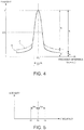
- FIG. 3 is a graph illustrating a relation between Allan variance (frequency precision) and a measurement time of an output signal of the atomic oscillator illustrated in FIG. 1 .
- FIG. 4 is a diagram illustrating a result illustrated in FIG. 3 based on a waveform of an EIT signal.
- FIG. 5 is a diagram schematically illustrating a frequency spectrum of light emitted from a light source illustrated in FIG. 1 .
- FIG. 6 is a graph illustrating an example of characteristics (a relation between a light source output and a bias current to be supplied) of the light source.
- FIG. 7 is a schematic diagram illustrating an overall configuration of an atomic oscillator according to a second embodiment.
- FIG. 8 is a diagram illustrating an embodiment of an electronic apparatus.
- FIG. 9 is a diagram illustrating an embodiment of a vehicle.
- FIG. 1 is a schematic diagram illustrating an overall configuration of an atomic oscillator according to a first embodiment.
- An atomic oscillator 1 illustrated in FIG. 1 is an atomic oscillator that uses coherent population trapping (CPT) in which a phenomenon occurs in which two pieces of resonance light are transmitted without being absorbed by alkali metal atoms when the two pieces of resonance light with specific different wavelengths are simultaneously radiated to the alkali metal atoms.
- CPT coherent population trapping
- the coherent population trapping phenomenon is also called the electromagnetically induced transparency (EIT) phenomenon.
- the atomic oscillator 1 includes a package unit 2 and a controller 10 that is electrically connected to the package unit 2 .
- the package unit 2 includes a light source 22 (light source unit) that emits light, an atomic cell 21 (gas cell) in which, for example, alkali metal atoms such as rubidium atoms or cesium atoms are sealed, and a light detector 23 (light detection unit), which are accommodated in a package (not illustrated).
- the controller 10 includes a detector circuit 31 , a modulation circuit 32 , a low-frequency oscillator 33 , a driving circuit 35 , a detector circuit 42 , a voltage controlled crystal oscillator 43 (VCXO), a modulation circuit 44 , a low-frequency oscillator 45 , a phase synchronization circuit 46 (Phase Locked Loop (PLL)), and an automatic gain control circuit 47 (automatic gain control amplifier (AGC)) which are installed outside of the package of the package unit 2 . At least a part of the controller 10 may be accommodated inside the package unit 2 .
- the driving circuit 35 supplies the light source 22 with a driving current obtained by superimposing a modulated current on a bias current.
- the light source 22 emits light with a central wavelength according to a current value of the bias current and two pieces of sideband light (first light and second light) with wavelengths deviating from the wavelength of the light on both sides of the wavelength by a wavelength according to a frequency of the modulated current.
- the two pieces of sideband light pass through the atomic cell 21 and are detected by the light detector 23 .
- the detector circuit 31 , the modulation circuit 32 , and the low-frequency oscillator 33 function as a “bias current adjuster 30 ” that adjusts the current value of the bias current of the driving circuit 35 based on a detection result of the light detector 23 .
- the detector circuit 42 , the voltage controlled crystal oscillator 43 , the modulation circuit 44 , the low-frequency oscillator 45 , and the phase synchronization circuit 46 function as a “signal generator 40 ” that generates a microwave signal according to a transition frequency between two ground levels of the alkali metal atoms inside the atomic cell 21 based on a detection result of the light detector 23 .
- the signal generator 40 adjusts the frequency of the microwave signal to be used as the modulated current so that an EIT phenomenon is produced by the alkali metal atoms inside the atomic cell 21 and the above-described two pieces of sideband light, stabilizes an output signal of the voltage controlled crystal oscillator 43 (VCXO) at a predetermined frequency, and outputs the output signal as a clock signal of the atomic oscillator 1 .
- the automatic gain control circuit 47 adjusts the amplitude of the modulated current (microwave signal) from the signal generator 40 and inputs the modulated current to the driving circuit 35 .
- the driving circuit 35 the bias current adjuster 30 , and the automatic gain control circuit 47 function as a “light source adjuster 50 ” that adjusts the frequencies of the above-described two pieces of sideband light (the first light and the second light).
- the package unit 2 illustrated in FIG. 1 includes the light source 22 (the light source unit), the atomic cell 21 (gas cell), and the light detector 23 (light detection unit), as described above.
- the light source 22 is supplied with the driving current obtained by superimposing the modulated current on the bias current and emits the above-described two pieces of sideband light as first light and second light with mutually different frequencies (wavelengths).
- the light source 22 may be a light source that has the above-described function.
- the invention is not particularly limited.
- a semiconductor laser such as a vertical cavity surface emitting laser (VCSEL) can be exemplified.
- alkali metal such as rubidium, cesium, or sodium in a gaseous form is sealed inside the atomic cell 21 .
- a noble gas such as argon or neon or an inert gas such as nitrogen may be sealed as a buffer gas along with the alkali metal gas, as necessary.
- the alkali metal atom has energy levels of three level systems formed by two different ground levels (first and second ground levels) and an excited level.
- the first ground level is an energy level lower than the second ground level.
- resonance light first resonance light
- second resonance light that has a frequency ⁇ 2 equivalent to an energy difference between the second ground level and the excited level
- an electromagnetically induced transparency (EIT) phenomenon occurs in which both the first resonance light and the second resonance light are transmitted without being absorbed in the alkali metal atoms.
- the EIT phenomenon occurs when the first resonance light and the second resonance light are simultaneously radiated to the alkali metal atoms and a frequency difference ( ⁇ 1 ⁇ 2 ) between the frequency ⁇ 1 of the first resonance light and the frequency ⁇ 2 of the second resonance light matches a frequency ⁇ 0 equivalent to an energy difference ⁇ E between the first and second ground levels.
- optical absorptance (light transmittance) in the alkali metal atoms of the first resonance light and the second resonance light is changed according to the frequency difference ( ⁇ 1 ⁇ 2 ), the EIT phenomenon occurs when the frequency difference ( ⁇ 1 ⁇ 2 ) matches the frequency ⁇ 0 , and the intensities of the first resonance light and the second resonance light transmitted through the alkali metal atoms are steeply increased.
- a steep signal generated by the EIT phenomenon is referred to as an EIT signal.
- the EIT signal has a fixed value decided according to a type of alkali metal atom. Therefore, by using the EIT signal as a standard, the high precise oscillator can be configured.
- the alkali metal atoms are cesium atoms
- the frequency ⁇ 0 equivalent to the energy difference ⁇ E is 9.1926 GHz. Therefore, when two types of light in which the frequency difference ( ⁇ 1 ⁇ 2 ) is 9.1926 GHz are simultaneously radiated to cesium atoms, the EIT signal is detected.
- the atomic cell 21 is heated by a heater (not illustrated) driven based on a detection result of a temperature sensor (not illustrated) that detects the temperature of the atomic cell 21 .
- a temperature sensor not illustrated
- the alkali metal in the atomic cell 21 can be maintained in a gaseous form of an appropriate density.
- a magnetic field generator (not illustrated) that has a coil or the like applying a magnetic field to the alkali metal by conduction is installed near the atomic cell 21 . According to the magnetic field from the magnetic field generator, a gap between a plurality of different energy levels at which the alkali metal atoms are degenerated can be spread by Zeeman splitting to improve a resolution. As a result, it is possible to improve precision of the oscillation frequency of the atomic oscillator 1 .
- Optical components such as a wavelength plate, a light reduction filter, a lens, and a polarization plate may be disposed between the light source 22 and the atomic cell 21 described above.
- the light detector 23 has a function of receiving and detecting the light (the first light and the second light) transmitted through the atomic cell 21 and outputting a detection signal according to the intensity of the detected light.
- the light detector 23 is not particularly limited as long as the intensity of the light described above can be detected.
- a light detector light-receiving element
- a photodiode can be exemplified.
- the controller 10 includes the bias current adjuster 30 , the driving circuit 35 , the signal generator 40 , and the automatic gain control circuit 47 .
- the bias current adjuster 30 includes the detector circuit 31 , the modulation circuit 32 , and the low-frequency oscillator 33 .
- the detector circuit 31 synchronously detects an output signal of the light detector 23 at a low frequency of a few Hz to a few hundreds of Hz (for each fourth period) using an output signal (oscillation signal) of the low-frequency oscillator 33 oscillated at the frequency.
- the modulation circuit 32 modulates an output signal of the detector circuit 31 using an output signal (oscillation signal) of the low-frequency oscillator 33 as a modulation signal so that the detector circuit 31 can perform detection.
- the driving circuit 35 minutely adjusts a bias current according to the output signal of the modulation circuit 32 and sets a bias current to be supplied to the light source 22 (sets a central wavelength of the light emitted from the light source 22 ). In this way, the central wavelength of the light emitted by the light source 22 is controlled (minutely adjusted) to be stabilized by a feedback loop passing through the light source 22 , the atomic cell 21 , the light detector 23 , the detector circuit 31 , the modulation circuit 32 , and the driving circuit 35 .
- the bias current adjuster 30 adjusts a current value of the bias current set by the driving circuit 35 for each period (the fourth period) corresponding to the oscillation frequency of the low-frequency oscillator 33 .
- the adjusted period (the fourth period) is longer than a detection period (a first period) in the signal generator 40 to be described below.
- the feedback loop may be subjected to analog processing or may be subjected to digital processing.
- the driving circuit 35 superimposes the modulated current from the automatic gain control circuit 47 to be described below on the minutely adjusted bias current, as described above, and supplies the superimposed current to the light source 22 .
- the light emitted from the light source 22 is subjected to frequency modulation in accordance with the modulated current, a plurality of pairs of pieces of light with frequencies deviating on both sides of the central frequency by a frequency of the modulated current are generated as the sideband light along with light with a central frequency according to the bias current.
- the signal generator 40 includes the detector circuit 42 , the voltage controlled crystal oscillator 43 , the modulation circuit 44 , the low-frequency oscillator 45 , and the phase synchronization circuit 46 .
- the detector circuit 42 synchronously detects an output signal of the light detector 23 at a low frequency of a few of Hz to a few hundreds of Hz (for each first period) using an oscillated signal of the low-frequency oscillator 45 oscillated at the low-frequency. Then, the voltage controlled crystal oscillator 43 (VCXO) minutely adjusts the oscillation frequency of the voltage controlled crystal oscillator 43 (VCXO) according to a magnitude of the output signal of the detector circuit 42 .
- the voltage controlled crystal oscillator 43 (VCXO) is oscillated at a low frequency of a few tens of Hz to a few hundreds of Hz, for example.
- the modulation circuit 44 modulates an output signal of the voltage controlled crystal oscillator 43 (VCXO) using an oscillated signal of the low-frequency oscillator 45 as a modulation signal so that the detector circuit 42 can perform detection.
- VXO voltage controlled crystal oscillator 43
- the signal generator 40 configured to include the detector circuit 42 , the voltage controlled crystal oscillator 43 , the modulation circuit 44 , the low-frequency oscillator 45 , and the phase synchronization circuit 46 generates a microwave signal (modulated current) according to the transition frequency between two ground levels of the alkali metal atoms inside the atomic cell 21 based on a result obtained by detecting the detection signal of the light detector 23 for each period (first period) corresponding to the oscillation frequency of the low-frequency oscillator 45 .
- the automatic gain control circuit 47 is an amplification circuit (amplifier) that automatically adjusts an amplification factor (gain) so that the amplitude of the signal (modulated current) from the phase synchronization circuit 46 is constant. That is, the automatic gain control circuit 47 has an amplification function of amplifying the modulated current from the phase synchronization circuit 46 and an automatic gain control function of adjusting an amplification factor of the amplification function so that the amplitude of the modulated current from the phase synchronization circuit 46 becomes a preset constant amplitude.
- the modulated current with the preset constant amplitude can be obtained by removing a variation in the amplitude of the modulated current caused due to the variation in the installation environment.
- the automatic gain control circuit 47 adjusts the amplitude of the microwave signal from the phase synchronization circuit 46 for each period (third period) longer than the detection period (the first period) in the signal generator 40 .
- the automatic gain control circuit 47 includes an amplifier 471 (AMP), a level detector 472 , and a filter 473 .
- the amplifier 471 has a function of amplifying and outputting the modulated current from the phase synchronization circuit 46 and adjusts the amplification factor according to a signal from the filter 473 .
- the modulated current output from the amplifier 471 is input to each of the driving circuit 35 and the level detector 472 .
- the level detector 472 detects an output level of the modulated current from the amplifier 471 at a predetermined period (third period) and outputs a signal according to a detection result.
- the signal from the level detector 472 is input to the amplifier 471 via the filter 473 with a bandwidth corresponding to the detection period of the level detector 472 .
- the configuration of the automatic gain control circuit 47 is not limited to the illustrated configuration.
- a buffer circuit may be installed between the level detector 472 and the filter 473 .
- the output signal of the automatic gain control circuit 47 is input to the driving circuit 35 as a current (modulated current) of a modulation frequency fm.
- a pair of pieces of sideband light emitted by the light source 22 is controlled (minutely adjusted) such that the sideband light turns into a pair of pieces of resonance light producing the EIT phenomenon in the alkali metal atoms by a feedback loop passing through the light source 22 , the atomic cell 21 , the light detector 23 , the detector circuit 42 , the voltage controlled crystal oscillator 43 , the modulation circuit 44 , the phase synchronization circuit 46 , the automatic gain control circuit 47 , and the driving circuit 35 .
- a loop bandwidth of the feedback loop is the same as the oscillation frequency of the low-frequency oscillator 45 .
- the EIT signal which is a steep signal generated by the EIT phenomenon is detected by the light detector 23 and the output signal of the voltage controlled crystal oscillator 43 is stabilized at a predetermined frequency using the EIT signal as a standard signal. Then, the output signal of the voltage controlled crystal oscillator 43 is output to the outside. At this time, the frequency of the output signal of the voltage controlled crystal oscillator 43 may be converted into a desired frequency at a predetermined frequency conversion ratio by, for example, a frequency conversion circuit (not illustrated) such as a direct digital synthesizer (DDS), as necessary.
- DDS direct digital synthesizer
- the bias current adjuster 30 adjusts a current value of the bias current of the driving circuit 35 based on a detection result of the light detector 23 and the signal generator 40 adjusts the frequency of the modulated current of the driving circuit 35 .
- the automatic gain control circuit 47 adjusts the current value (level) of the modulated current from the signal generator 40 and inputs the adjusted current value to the driving circuit 35 .
- the signal generator 40 stabilizes the output signal of the voltage controlled crystal oscillator 43 (VCXO) at the predetermined frequency so that the above-described two pieces of sideband light and the EIT phenomenon occur by the alkali metal atoms inside the atomic cell 21 , and outputs the output signal as a clock signal of the atomic oscillator 1 .
- VXO voltage controlled crystal oscillator 43
- the light source adjuster 50 configured to include the driving circuit 35 , the bias current adjuster 30 , and the automatic gain control circuit 47 adjusts the frequencies of the above-described two pieces of sideband light (the first light and the second light) for each period (second period) longer than the detection period (the first period) in the signal generator 40 .
- the adjustment period (the second period) is identical to a shorter period between the adjustment period (fourth period) in the above-described bias current adjuster 30 and the adjustment period (the third period) in the automatic gain control circuit 47 .
- FIG. 2 is a graph illustrating a relation between a loop gain and a loop bandwidth of a control loop included in the atomic oscillator illustrated in FIG. 1 .
- FIG. 3 is a graph illustrating a relation between Allan variance (frequency precision) and a measurement time of an output signal of the atomic oscillator illustrated in FIG. 1 .
- FIG. 4 is a diagram illustrating a result illustrated in FIG. 3 based on a waveform of an EIT signal.
- FIG. 5 is a diagram schematically illustrating a frequency spectrum of light emitted from a light source illustrated in FIG. 1 .
- FIG. 6 is a graph illustrating an example of characteristics (a relation between a light source output and a bias current to be supplied) of the light source.
- the atomic oscillator 1 includes the atomic cell 21 in which the alkali metal atoms are sealed, the light source 22 that is a “light source unit” radiating the first light and the second light with mutually different frequencies to the atomic cell 21 , and the light detector 23 that is a “light detection unit” detecting the first light and the second light transmitted through the atomic cell 21 and outputting a detection signal according to the detection intensity (hereinafter simply referred to as a “detection signal”).
- the atomic oscillator 1 includes the signal generator 40 that generates a microwave signal according to a transition frequency between two ground levels of the alkali metal atoms inside the atomic cell 21 based on a result obtained by detecting the detection signal of the light detector 23 for each first period (hereinafter simply referred to as the “first period”) and the light source adjuster 50 that adjusts the frequencies of the first light and the second light from the light source 22 for each second period longer than the first period (hereinafter simply referred to as the “second period”).
- first period a transition frequency between two ground levels of the alkali metal atoms inside the atomic cell 21 based on a result obtained by detecting the detection signal of the light detector 23 for each first period
- the light source adjuster 50 that adjusts the frequencies of the first light and the second light from the light source 22 for each second period longer than the first period
- the light source adjuster 50 adjusts the frequencies of the first light and the second light from the light source 22 to stabilize these frequencies. In this way, by adjusting the frequencies of the first light and the second light from the light source 22 , it is possible to reduce deterioration of the short-term frequency stability due to a variation (disturbance) of the installation environment. By causing the period (the second period) at which the frequencies of the first light and the second light are adjusted to be longer than the period (the first period) at which the signal generator 40 detects the detection signal, it is possible to reduce the deterioration in the short-term frequency stability due to the adjustment.
- the light source adjuster 50 includes the driving circuit 35 that drives the light source 22 by inputting the driving current obtained by superimposing the modulated current based on the microwave signal from the signal generator 40 on the bias current to the light source 22 which is the “light source unit” and the automatic gain control circuit 47 that adjusts the amplitude of the microwave signal from the signal generator 40 for each third period longer than the first period (hereinafter simply referred to as the “third period”).
- the third period the third period longer than the first period
- the period (the third period) at which the modulated current is adjusted is longer than the period (the first period) at which the detection signal is detected at the time of generating the microwave signal, it is possible to reduce the deterioration in the short-term frequency stability due to the adjustment.
- a loop bandwidth of the control loop of the automatic gain control circuit 47 is less than a loop bandwidth of a feedback loop passing through the light source 22 , the atomic cell 21 , the light detector 23 , the detector circuit 42 , the voltage controlled crystal oscillator 43 , the modulation circuit 44 , the phase synchronization circuit 46 , the automatic gain control circuit 47 , and the driving circuit 35 described above (hereinafter also referred to as an “atomic resonance loop”).
- a indicated by a one-dot chain line in FIG. 2 indicates a relation between a loop bandwidth and a loop gain in the atomic resonance loop.
- the loop bandwidth in the atomic resonance loop is the same as a reciprocal of the first period.
- B indicated by a solid line in FIG. 2 indicates a relation between a loop gain and a loop bandwidth in the control loop of the automatic gain control circuit 47 .
- the loop bandwidth in the control loop of the automatic gain control circuit 47 is the same as a reciprocal of the third period.
- the third period is longer than the first period (C indicated by a solid line in FIG. 3 )
- the third period is shorter than the first period (D indicated by a dotted line in FIG. 3 )
- the light source adjuster 50 includes the bias current adjuster 30 that adjusts the current value of the bias current set in the driving circuit 35 for each fourth period longer than the first period (hereinafter simply referred to as the “fourth period”). In this way, it is possible to stabilize the bias current input to the light source 22 and reduce the variation in the short-term frequency stability due to the variation (disturbance) in the installation environment.
- the period (the fourth period) at which the bias current is adjusted to be longer than the period (the first period) at which the detection signal is detected at the time of generating the microwave signal, it is possible to reduce the deterioration in the short-term frequency stability due to the adjustment.
- the obtained effect is the same as the effect obtained by causing the third period to be longer than the first period.
- the third period preferably differs from the fourth period from the viewpoint of control easiness.
- a magnitude relation between the periods can be decided according to, for example, the characteristics in the light source 22 .
- the fourth period is preferably shorter than the third period. In this way, it is possible to effectively reduce a variation in the central wavelength of the light from the light source 22 . As a result, it is possible to improve stability of the wavelengths of the first light and the second light. More specifically, as illustrated in FIG.
- the light source 22 emits light with a central frequency f 0 according to the current value of the bias current and two pieces of sideband light (the first light and the second light) with frequencies f 1 and f 2 shifted by a frequency fm of the modulated current on both sides of the central frequency f 0 of the light.
- the fourth period is shorter than the third period, it is possible to first stabilize the central frequency f 0 and stabilize the frequencies f 1 and f 2 from this state. Therefore, it is possible to further reduce the shift of the central frequency f 0 .
- the fourth period is preferably longer than the third period. In this way, it is possible to effectively reduce a variation in the central wavelength of the light from the light source 22 . As a result, it is possible to improve stability of the wavelengths of the first light and the second light. More specifically, for example, as illustrated in FIG. 6 , when the nonlinearity of the output characteristics of the light source 22 with respect to the bias current is relatively high and the microwave signal varies, the bias current is accordingly changed from I 1 to I 2 of the light source 22 , which results in the change of the output of the light source from P 1 to P 2 . Thus, it is difficult to stably adjust the bias current. Accordingly, by causing the fourth period to be longer than the third period, it is possible to first stabilize the microwave signal. As a result, it is possible to stably adjust the bias current.
- T3/T4 is preferably equal to or greater than 0.1 and equal to or less than 10 and is more preferably equal to or greater than 0.5 and equal to or less than 2.0.
- the second period is a period longer than the first period and is identical to a shorter period between the third and fourth periods.
- the second period is preferably equal to or less than (0.1/T) second when the installation environment temperature of the atomic oscillator 1 varies at a variation speed T [° C./second]. In this way, it is possible to reduce a variation in the short-term frequency stability due to the variation in the installation environment temperature.
- the first period is preferably equal to or greater than 1/150 seconds and equal to or less than 1/50 seconds. That is, the loop bandwidth in the atomic resonance loop is preferably equal to or greater than 50 Hz and equal to or less than 150 Hz. In this way, the signal generator 40 can appropriately generate a microwave signal.
- the second period is preferably equal to or less than 1 second. That is, the frequency adjusted by the bias current adjuster 30 and the frequency adjusted by the automatic gain control circuit 47 are preferably equal to or greater than 1 Hz. In this way, it is possible to reduce the variation in the short-term frequency stability due to the variation in a general installation environment.
- FIG. 7 is a schematic diagram illustrating an overall configuration of an atomic oscillator according to a second embodiment.
- the embodiment is the same as the above-described first embodiment except that the invention is applied in an optical microwave double resonance scheme.
- An atomic oscillator 1 A illustrated in FIG. 7 is an atomic oscillator that oscillates based on energy transition of alkali metal atoms such as rubidium using the optical microwave double resonance phenomenon.
- the optical microwave double resonance phenomenon is a phenomenon generated when resonance light that has a frequency equivalent to an energy difference between the first ground level and the excited level and a microwave that has a frequency equivalent to an energy difference between the first and second ground levels are radiated to the alkali metal atoms at the same time.
- the atomic oscillator 1 A includes a package unit 2 A and a controller 10 A electrically connected to the package unit 2 A.
- the package unit 2 A includes a light source 22 A (light source unit), an atomic cell 21 (gas cell), a light detector 23 (light detection unit), and an antenna 24 which are accommodated in a package (not illustrated).
- a light source 22 A light source unit
- an atomic cell 21 gas cell
- a light detector 23 light detection unit
- an antenna 24 which are accommodated in a package (not illustrated).
- the light source 22 A is, for example, a lamp in which an alkali metal is sealed.
- a semiconductor laser such as a vertical cavity surface emitting laser (VCSEL) can be used as the light source 22 A.
- VCSEL vertical cavity surface emitting laser
- the antenna 24 has a function of releasing (radiating) microwaves to be radiated to the alkali metal atoms inside the atomic cell 21 .
- the antenna 24 is not particularly limited as long as microwaves can be released. Any of various antennas can be used.
- the antenna 24 includes a substrate formed of a dielectric material and a radiation pattern and a reflector installed on the surface of the substrate and formed of a conductive material.
- the atomic cell 21 and the antenna are accommodated inside a cavity (not illustrated) configured such that stationary waves with a frequency equivalent to the energy difference between the first and second ground levels of the alkali metal atoms are generated. Accordingly, when the frequency of the microwave from the antenna 24 becomes the frequency equivalent to the energy difference between the first and second ground levels of the alkali metal atoms, the microwave from the antenna 24 is resonated inside the cavity.
- the controller 10 A controls the frequency of the microwave released from the antenna 24 such that the optical microwave double resonance phenomenon is produced based on a detection result of the light detector 23 .
- the controller 10 A includes a driving circuit 35 A, a signal generator 40 , and an automatic gain control circuit 47 .
- the driving circuit 35 A drives the light source 22 A so that the frequency of light from the light source 22 A becomes the frequency equivalent to the energy difference between the first ground level and the excited level of the alkali metal atoms.
- a modulated current from the automatic gain control circuit 47 is supplied to the antenna 24 .
- the automatic gain control circuit 47 is a microwave adjuster 50 A that adjusts the amplitude of the microwave from the antenna 24 for each second period longer than the first period.
- the atomic oscillator 1 A that has the foregoing configuration includes an atomic cell 21 in which alkali metal atoms are sealed, a light source 22 A which is a “light source unit” radiating light to the atomic cell 21 , and a light detector 23 which is a “light detection unit” detecting the light transmitted through the atomic cell 21 and outputting a detection signal according to a detected intensity.
- the atomic oscillator 1 A includes a signal generator 40 that generates a microwave signal according to the transition frequency between two ground levels of the alkali metal atoms inside the atomic cell 21 based on a result obtained by detecting the detection signal for each first period, the antenna 24 that radiates the microwave to the atomic cell 21 when a signal based on the microwave signal from the signal generator 40 is input, and the microwave adjuster 50 A that adjusts the amplitude of the microwave from the antenna 24 for each second period longer than the first period.
- the atomic oscillator 1 A adjusts the amplitude of the microwave from the antenna 24 , it is possible to reduce the deterioration in the short-term frequency stability due to a variation (disturbance) in the installation environment.
- the period (the second period) at which the amplitude of the microwave from the antenna 24 is adjusted to be longer than the period (the first period) at which the signal generator 40 detects a detection signal, it is possible to reduce the deterioration in the short-term frequency stability due to the adjustment.
- FIG. 8 is a diagram illustrating an embodiment of an electronic apparatus.
- a positioning system 100 (electronic apparatus) illustrated in FIG. 8 is configured to include a GPS satellite 200 , abase station apparatus 300 , and a GPS reception apparatus 400 .
- the GPS satellite 200 transmits positioning information (a GPS signal).
- the base station apparatus 300 includes a reception apparatus 302 that receives the positioning information with high precision from the GPS satellite 200 via an antenna 301 installed at, for example, an electronic standard point (GPS continuous observation station) and a transmission apparatus 304 that transmits the positional information received by the reception apparatus 302 via an antenna 303 .
- a reception apparatus 302 that receives the positioning information with high precision from the GPS satellite 200 via an antenna 301 installed at, for example, an electronic standard point (GPS continuous observation station) and a transmission apparatus 304 that transmits the positional information received by the reception apparatus 302 via an antenna 303 .
- the reception apparatus 302 is an electronic apparatus that includes the above-described atomic oscillator 1 as a standard frequency oscillation source.
- the reception apparatus 302 has excellent reliability.
- the positional information received by the reception apparatus 302 is transmitted in real time by the transmission apparatus 304 .
- the GPS reception apparatus 400 includes a satellite receiver 402 that receives the positioning information from the GPS satellite 200 via an antenna 401 and a base station receiver 404 that receives the positional information from the base station apparatus 300 via an antenna 403 .
- the reception apparatus 302 which is an “electronic apparatus” included in the above-described positioning system 100 includes the atomic oscillator 1 , as described above. As described above, the atomic oscillator 1 can reduce the deterioration in the short-term frequency stability even when the installation environment varies. Therefore, by using a signal for high frequency stability regardless of the installation environment of the reception apparatus 302 , the reception apparatus 302 can function highly.
- the reception apparatus 302 may include the atomic oscillator 1 A instead of the atomic oscillator 1 or in addition to the atomic oscillator 1 .
- the electronic apparatus including the atomic oscillator according to the invention is not limited to the above-described electronic apparatus.
- the invention can be applied to, for example, a smartphone, a tablet terminal, a timepiece, a mobile phone, a digital still camera, an ink jet ejection apparatus (for example, an ink jet printer), a personal computer (a mobile personal computer or a laptop personal computer), a television, a video camera, a video tape recorder, a car navigation apparatus, a pager, an electronic organizer (also including a communication function unit), an electronic dictionary, a calculator, an electronic game apparatus, a word processor, a workstation, a television telephone, a security television monitor, electronic binoculars, a POS terminal, a medical apparatus (for example, an electronic thermometer, a blood-pressure meter, a blood-sugar meter, an electrocardiographic apparatus, an ultrasonic diagnostic apparatus, or an electronic endoscopy), a fish finder, various measurement apparatuses, meters (for example, meters for cars
- FIG. 9 is a diagram illustrating an embodiment of a vehicle.
- a vehicle 1500 includes a body 1501 and four wheels 1502 and is configured to rotate the wheels 1502 by a power source (engine) (not illustrated) installed in the body 1501 .
- the vehicle 1500 contains the atomic oscillator 1 .
- the above-described vehicle 1500 includes the atomic oscillator 1 , as described above.
- the atomic oscillator 1 can reduce deterioration of short-term frequency stability even when an installation environment varies. Therefore, the vehicle 1500 can function highly using a signal for high frequency stability regardless of the position of the vehicle 1500 .
- the vehicle 1500 may include the atomic oscillator 1 A instead of the atomic oscillator 1 or in addition to the atomic oscillator 1 .
- each unit of the atomic oscillator, the electronic apparatus, and the vehicle can be substituted with any configuration that has the same function. Any configuration can be added.
Landscapes
- Physics & Mathematics (AREA)
- General Physics & Mathematics (AREA)
- Spectroscopy & Molecular Physics (AREA)
- Life Sciences & Earth Sciences (AREA)
- Ecology (AREA)
- Stabilization Of Oscillater, Synchronisation, Frequency Synthesizers (AREA)
Applications Claiming Priority (2)
| Application Number | Priority Date | Filing Date | Title |
|---|---|---|---|
| JP2016-174979 | 2016-09-07 | ||
| JP2016174979A JP6753232B2 (ja) | 2016-09-07 | 2016-09-07 | 原子発振器、電子機器および移動体 |
Publications (2)
| Publication Number | Publication Date |
|---|---|
| US20180069557A1 US20180069557A1 (en) | 2018-03-08 |
| US10566983B2 true US10566983B2 (en) | 2020-02-18 |
Family
ID=61281046
Family Applications (1)
| Application Number | Title | Priority Date | Filing Date |
|---|---|---|---|
| US15/685,293 Expired - Fee Related US10566983B2 (en) | 2016-09-07 | 2017-08-24 | Atomic oscillator, electronic apparatus, and control method |
Country Status (3)
| Country | Link |
|---|---|
| US (1) | US10566983B2 (ja) |
| JP (1) | JP6753232B2 (ja) |
| CN (1) | CN107800432A (ja) |
Families Citing this family (4)
| Publication number | Priority date | Publication date | Assignee | Title |
|---|---|---|---|---|
| CN109194329A (zh) * | 2018-07-16 | 2019-01-11 | 北京无线电计量测试研究所 | 一种微波源 |
| US20230095704A1 (en) * | 2020-03-16 | 2023-03-30 | Oxford University Innovation Limited | Oscillation device |
| JP7443862B2 (ja) * | 2020-03-23 | 2024-03-06 | セイコーエプソン株式会社 | 共鳴発生方法及び原子発振器 |
| US20220156624A1 (en) * | 2020-11-13 | 2022-05-19 | ColdQuanta, Inc. | Hybrid-cycle quantum-clock frequency regulation |
Citations (5)
| Publication number | Priority date | Publication date | Assignee | Title |
|---|---|---|---|---|
| JP2001036405A (ja) | 1999-07-22 | 2001-02-09 | Fujitsu Ltd | 原子発振器 |
| US6320472B1 (en) | 1999-01-26 | 2001-11-20 | Kernco, Inc. | Atomic frequency standard |
| US8253497B2 (en) * | 2010-03-02 | 2012-08-28 | Seiko Epson Corporation | Atomic oscillator |
| US20130176081A1 (en) * | 2012-01-11 | 2013-07-11 | Seiko Epson Corporation | Interference filter, optical module, and electronic apparatus |
| US20180198456A1 (en) * | 2016-12-20 | 2018-07-12 | Seiko Epson Corporation | Quantum interference device, atomic oscillator, and electronic apparatus |
Family Cites Families (10)
| Publication number | Priority date | Publication date | Assignee | Title |
|---|---|---|---|---|
| JP3172777B2 (ja) * | 1992-05-19 | 2001-06-04 | アンリツ株式会社 | 原子発振器 |
| JP5381400B2 (ja) * | 2009-02-06 | 2014-01-08 | セイコーエプソン株式会社 | 量子干渉装置、原子発振器、および磁気センサー |
| JP5429469B2 (ja) * | 2009-09-07 | 2014-02-26 | セイコーエプソン株式会社 | 量子干渉装置、原子発振器及び磁気センサー |
| JP2011091476A (ja) * | 2009-10-20 | 2011-05-06 | Seiko Epson Corp | 原子発振器 |
| JP6094730B2 (ja) * | 2012-11-07 | 2017-03-15 | セイコーエプソン株式会社 | 周波数変換回路、原子発振器、電子機器及び周波数変換回路の制御方法 |
| JP6201352B2 (ja) * | 2013-03-13 | 2017-09-27 | 株式会社リコー | 原子発振器及びその制御方法 |
| JP6210192B2 (ja) * | 2013-03-27 | 2017-10-11 | セイコーエプソン株式会社 | 原子発振器、原子発振器の製造方法 |
| JP2015070415A (ja) * | 2013-09-27 | 2015-04-13 | セイコーエプソン株式会社 | 原子発振器、電子機器、移動体及び原子発振器の製造方法 |
| JP2015057841A (ja) * | 2014-10-31 | 2015-03-26 | セイコーエプソン株式会社 | 量子干渉装置 |
| JP2016092146A (ja) * | 2014-10-31 | 2016-05-23 | セイコーエプソン株式会社 | 量子干渉装置、原子発振器、電子機器および移動体 |
-
2016
- 2016-09-07 JP JP2016174979A patent/JP6753232B2/ja active Active
-
2017
- 2017-08-18 CN CN201710711853.XA patent/CN107800432A/zh active Pending
- 2017-08-24 US US15/685,293 patent/US10566983B2/en not_active Expired - Fee Related
Patent Citations (6)
| Publication number | Priority date | Publication date | Assignee | Title |
|---|---|---|---|---|
| US6320472B1 (en) | 1999-01-26 | 2001-11-20 | Kernco, Inc. | Atomic frequency standard |
| JP2001036405A (ja) | 1999-07-22 | 2001-02-09 | Fujitsu Ltd | 原子発振器 |
| US6300841B1 (en) | 1999-07-22 | 2001-10-09 | Fujitsu Limited | Atomic oscillator utilizing a high frequency converting circuit and an active, low-integral-number multiplier |
| US8253497B2 (en) * | 2010-03-02 | 2012-08-28 | Seiko Epson Corporation | Atomic oscillator |
| US20130176081A1 (en) * | 2012-01-11 | 2013-07-11 | Seiko Epson Corporation | Interference filter, optical module, and electronic apparatus |
| US20180198456A1 (en) * | 2016-12-20 | 2018-07-12 | Seiko Epson Corporation | Quantum interference device, atomic oscillator, and electronic apparatus |
Also Published As
| Publication number | Publication date |
|---|---|
| JP6753232B2 (ja) | 2020-09-09 |
| US20180069557A1 (en) | 2018-03-08 |
| JP2018042114A (ja) | 2018-03-15 |
| CN107800432A (zh) | 2018-03-13 |
Similar Documents
| Publication | Publication Date | Title |
|---|---|---|
| US10566983B2 (en) | Atomic oscillator, electronic apparatus, and control method | |
| US10432205B2 (en) | Quantum interference device, atomic oscillator, and electronic apparatus | |
| US10659067B2 (en) | Alkali-metal vapor cell atomic clock system | |
| US10312924B2 (en) | Timing signal generation device, electronic device, and moving object | |
| JP6519169B2 (ja) | 原子共鳴遷移装置、原子発振器、時計、電子機器および移動体 | |
| JP2011523787A (ja) | 自己混合干渉に基づく原子周波数取得装置 | |
| JP6686442B2 (ja) | 量子干渉装置、原子発振器、および電子機器 | |
| JP6094730B2 (ja) | 周波数変換回路、原子発振器、電子機器及び周波数変換回路の制御方法 | |
| JP2015070415A (ja) | 原子発振器、電子機器、移動体及び原子発振器の製造方法 | |
| US9935642B2 (en) | Quantum interference device, atomic oscillator, electronic apparatus, and moving object | |
| US10333537B2 (en) | Atomic oscillator and a method of generating atomic oscillation | |
| JP2017188712A (ja) | 量子干渉装置、原子発振器、電子機器および移動体 | |
| US10804915B2 (en) | Atomic oscillator and frequency signal generation system | |
| Zhu et al. | A novel scheme of microwave generation based on heterodyne phase locking of an OEO | |
| JP6686640B2 (ja) | 量子干渉装置、原子発振器、および電子機器 | |
| US10826509B2 (en) | Method of controlling atomic oscillator, atomic oscillator, and frequency signal generation system | |
| US10348052B1 (en) | Tunable laser system and method based on dual sideband locking | |
| JP2015041726A (ja) | 量子干渉装置、原子発振器、電子機器、および移動体 | |
| JP6662061B2 (ja) | 量子干渉装置、原子発振器、電子機器および移動体 | |
| JP6897493B2 (ja) | 原子発振器、電子機器及び移動体 | |
| JP2022098666A (ja) | 原子発振器及び周波数信号生成システム | |
| JP2022127514A (ja) | 波長制御装置、波長制御方法、差分吸収ライダー装置 | |
| JPH09186388A (ja) | 波長安定化光源 | |
| JP2015012528A (ja) | 原子発振器、電子機器、移動体、およびgpsモジュール |
Legal Events
| Date | Code | Title | Description |
|---|---|---|---|
| AS | Assignment |
Owner name: SEIKO EPSON CORPORATION, JAPAN Free format text: ASSIGNMENT OF ASSIGNORS INTEREST;ASSIGNORS:MAKI, YOSHIYUKI;TANAKA, NORIAKI;SIGNING DATES FROM 20170818 TO 20170821;REEL/FRAME:043387/0543 |
|
| STPP | Information on status: patent application and granting procedure in general |
Free format text: NON FINAL ACTION MAILED |
|
| STPP | Information on status: patent application and granting procedure in general |
Free format text: RESPONSE TO NON-FINAL OFFICE ACTION ENTERED AND FORWARDED TO EXAMINER |
|
| STPP | Information on status: patent application and granting procedure in general |
Free format text: FINAL REJECTION MAILED |
|
| STPP | Information on status: patent application and granting procedure in general |
Free format text: RESPONSE AFTER FINAL ACTION FORWARDED TO EXAMINER |
|
| STPP | Information on status: patent application and granting procedure in general |
Free format text: NOTICE OF ALLOWANCE MAILED -- APPLICATION RECEIVED IN OFFICE OF PUBLICATIONS |
|
| STCF | Information on status: patent grant |
Free format text: PATENTED CASE |
|
| AS | Assignment |
Owner name: MICROCHIP TECHNOLOGY INCORPORATED, ARIZONA Free format text: ASSIGNMENT OF ASSIGNORS INTEREST;ASSIGNOR:SEIKO EPSON CORPORATION;REEL/FRAME:061301/0770 Effective date: 20220707 |
|
| FEPP | Fee payment procedure |
Free format text: MAINTENANCE FEE REMINDER MAILED (ORIGINAL EVENT CODE: REM.); ENTITY STATUS OF PATENT OWNER: LARGE ENTITY |
|
| LAPS | Lapse for failure to pay maintenance fees |
Free format text: PATENT EXPIRED FOR FAILURE TO PAY MAINTENANCE FEES (ORIGINAL EVENT CODE: EXP.); ENTITY STATUS OF PATENT OWNER: LARGE ENTITY |
|
| STCH | Information on status: patent discontinuation |
Free format text: PATENT EXPIRED DUE TO NONPAYMENT OF MAINTENANCE FEES UNDER 37 CFR 1.362 |
|
| FP | Lapsed due to failure to pay maintenance fee |
Effective date: 20240218 |