US10475813B2 - Ferroelectric memory device and method of manufacturing the same - Google Patents
Ferroelectric memory device and method of manufacturing the same Download PDFInfo
- Publication number
- US10475813B2 US10475813B2 US15/820,376 US201715820376A US10475813B2 US 10475813 B2 US10475813 B2 US 10475813B2 US 201715820376 A US201715820376 A US 201715820376A US 10475813 B2 US10475813 B2 US 10475813B2
- Authority
- US
- United States
- Prior art keywords
- layer
- superlattice structure
- oxide layer
- memory device
- ferroelectric
- Prior art date
- Legal status (The legal status is an assumption and is not a legal conclusion. Google has not performed a legal analysis and makes no representation as to the accuracy of the status listed.)
- Active
Links
- 238000004519 manufacturing process Methods 0.000 title claims description 16
- 239000000758 substrate Substances 0.000 claims abstract description 64
- 239000010410 layer Substances 0.000 claims description 342
- RVTZCBVAJQQJTK-UHFFFAOYSA-N oxygen(2-);zirconium(4+) Chemical compound [O-2].[O-2].[Zr+4] RVTZCBVAJQQJTK-UHFFFAOYSA-N 0.000 claims description 77
- 229910001928 zirconium oxide Inorganic materials 0.000 claims description 77
- 229910000449 hafnium oxide Inorganic materials 0.000 claims description 58
- WIHZLLGSGQNAGK-UHFFFAOYSA-N hafnium(4+);oxygen(2-) Chemical compound [O-2].[O-2].[Hf+4] WIHZLLGSGQNAGK-UHFFFAOYSA-N 0.000 claims description 58
- 239000000203 mixture Substances 0.000 claims description 52
- 238000000034 method Methods 0.000 claims description 46
- 230000028161 membrane depolarization Effects 0.000 claims description 42
- 238000009413 insulation Methods 0.000 claims description 35
- 230000008569 process Effects 0.000 claims description 15
- 239000010936 titanium Substances 0.000 claims description 10
- 238000002425 crystallisation Methods 0.000 claims description 9
- 230000008025 crystallization Effects 0.000 claims description 9
- 238000010438 heat treatment Methods 0.000 claims description 9
- 239000002356 single layer Substances 0.000 claims description 9
- 239000010949 copper Substances 0.000 claims description 8
- 229910052721 tungsten Inorganic materials 0.000 claims description 8
- 239000010937 tungsten Substances 0.000 claims description 8
- 238000000231 atomic layer deposition Methods 0.000 claims description 7
- 230000015572 biosynthetic process Effects 0.000 claims description 7
- XUIMIQQOPSSXEZ-UHFFFAOYSA-N Silicon Chemical compound [Si] XUIMIQQOPSSXEZ-UHFFFAOYSA-N 0.000 claims description 6
- 229910052710 silicon Inorganic materials 0.000 claims description 6
- 239000010703 silicon Substances 0.000 claims description 6
- RTAQQCXQSZGOHL-UHFFFAOYSA-N Titanium Chemical compound [Ti] RTAQQCXQSZGOHL-UHFFFAOYSA-N 0.000 claims description 5
- 229910052782 aluminium Inorganic materials 0.000 claims description 5
- XAGFODPZIPBFFR-UHFFFAOYSA-N aluminium Chemical compound [Al] XAGFODPZIPBFFR-UHFFFAOYSA-N 0.000 claims description 5
- 238000005229 chemical vapour deposition Methods 0.000 claims description 5
- TWNQGVIAIRXVLR-UHFFFAOYSA-N oxo(oxoalumanyloxy)alumane Chemical compound O=[Al]O[Al]=O TWNQGVIAIRXVLR-UHFFFAOYSA-N 0.000 claims description 5
- 229910052719 titanium Inorganic materials 0.000 claims description 5
- RYGMFSIKBFXOCR-UHFFFAOYSA-N Copper Chemical compound [Cu] RYGMFSIKBFXOCR-UHFFFAOYSA-N 0.000 claims description 4
- NRTOMJZYCJJWKI-UHFFFAOYSA-N Titanium nitride Chemical compound [Ti]#N NRTOMJZYCJJWKI-UHFFFAOYSA-N 0.000 claims description 4
- 229910052802 copper Inorganic materials 0.000 claims description 4
- 238000001704 evaporation Methods 0.000 claims description 4
- 229910001925 ruthenium oxide Inorganic materials 0.000 claims description 4
- WOCIAKWEIIZHES-UHFFFAOYSA-N ruthenium(iv) oxide Chemical compound O=[Ru]=O WOCIAKWEIIZHES-UHFFFAOYSA-N 0.000 claims description 4
- 229910021332 silicide Inorganic materials 0.000 claims description 4
- FVBUAEGBCNSCDD-UHFFFAOYSA-N silicide(4-) Chemical compound [Si-4] FVBUAEGBCNSCDD-UHFFFAOYSA-N 0.000 claims description 4
- 229910052715 tantalum Inorganic materials 0.000 claims description 4
- GUVRBAGPIYLISA-UHFFFAOYSA-N tantalum atom Chemical compound [Ta] GUVRBAGPIYLISA-UHFFFAOYSA-N 0.000 claims description 4
- MZLGASXMSKOWSE-UHFFFAOYSA-N tantalum nitride Chemical compound [Ta]#N MZLGASXMSKOWSE-UHFFFAOYSA-N 0.000 claims description 4
- 229910021341 titanium silicide Inorganic materials 0.000 claims description 4
- MTPVUVINMAGMJL-UHFFFAOYSA-N trimethyl(1,1,2,2,2-pentafluoroethyl)silane Chemical compound C[Si](C)(C)C(F)(F)C(F)(F)F MTPVUVINMAGMJL-UHFFFAOYSA-N 0.000 claims description 4
- WFKWXMTUELFFGS-UHFFFAOYSA-N tungsten Chemical compound [W] WFKWXMTUELFFGS-UHFFFAOYSA-N 0.000 claims description 4
- UONOETXJSWQNOL-UHFFFAOYSA-N tungsten carbide Chemical compound [W+]#[C-] UONOETXJSWQNOL-UHFFFAOYSA-N 0.000 claims description 4
- WQJQOUPTWCFRMM-UHFFFAOYSA-N tungsten disilicide Chemical compound [Si]#[W]#[Si] WQJQOUPTWCFRMM-UHFFFAOYSA-N 0.000 claims description 4
- -1 tungsten nitride Chemical class 0.000 claims description 4
- 229910021342 tungsten silicide Inorganic materials 0.000 claims description 4
- KJTLSVCANCCWHF-UHFFFAOYSA-N Ruthenium Chemical compound [Ru] KJTLSVCANCCWHF-UHFFFAOYSA-N 0.000 claims description 3
- 229910052581 Si3N4 Inorganic materials 0.000 claims description 3
- VYPSYNLAJGMNEJ-UHFFFAOYSA-N Silicium dioxide Chemical compound O=[Si]=O VYPSYNLAJGMNEJ-UHFFFAOYSA-N 0.000 claims description 3
- 229910052707 ruthenium Inorganic materials 0.000 claims description 3
- HQVNEWCFYHHQES-UHFFFAOYSA-N silicon nitride Chemical compound N12[Si]34N5[Si]62N3[Si]51N64 HQVNEWCFYHHQES-UHFFFAOYSA-N 0.000 claims description 3
- 229910052814 silicon oxide Inorganic materials 0.000 claims description 3
- 238000000151 deposition Methods 0.000 claims 1
- 239000000463 material Substances 0.000 description 26
- 239000013078 crystal Substances 0.000 description 9
- 230000010287 polarization Effects 0.000 description 9
- 239000002019 doping agent Substances 0.000 description 6
- 229910000577 Silicon-germanium Inorganic materials 0.000 description 4
- 229910052732 germanium Inorganic materials 0.000 description 3
- GNPVGFCGXDBREM-UHFFFAOYSA-N germanium atom Chemical compound [Ge] GNPVGFCGXDBREM-UHFFFAOYSA-N 0.000 description 3
- 230000001965 increasing effect Effects 0.000 description 3
- 229910052751 metal Inorganic materials 0.000 description 3
- 239000002184 metal Substances 0.000 description 3
- JBRZTFJDHDCESZ-UHFFFAOYSA-N AsGa Chemical compound [As]#[Ga] JBRZTFJDHDCESZ-UHFFFAOYSA-N 0.000 description 2
- IJGRMHOSHXDMSA-UHFFFAOYSA-N Atomic nitrogen Chemical compound N#N IJGRMHOSHXDMSA-UHFFFAOYSA-N 0.000 description 2
- GPXJNWSHGFTCBW-UHFFFAOYSA-N Indium phosphide Chemical compound [In]#P GPXJNWSHGFTCBW-UHFFFAOYSA-N 0.000 description 2
- LEVVHYCKPQWKOP-UHFFFAOYSA-N [Si].[Ge] Chemical compound [Si].[Ge] LEVVHYCKPQWKOP-UHFFFAOYSA-N 0.000 description 2
- 238000007792 addition Methods 0.000 description 2
- 239000011575 calcium Substances 0.000 description 2
- 238000000576 coating method Methods 0.000 description 2
- 239000004020 conductor Substances 0.000 description 2
- RKTYLMNFRDHKIL-UHFFFAOYSA-N copper;5,10,15,20-tetraphenylporphyrin-22,24-diide Chemical compound [Cu+2].C1=CC(C(=C2C=CC([N-]2)=C(C=2C=CC=CC=2)C=2C=CC(N=2)=C(C=2C=CC=CC=2)C2=CC=C3[N-]2)C=2C=CC=CC=2)=NC1=C3C1=CC=CC=C1 RKTYLMNFRDHKIL-UHFFFAOYSA-N 0.000 description 2
- 230000007547 defect Effects 0.000 description 2
- 238000009792 diffusion process Methods 0.000 description 2
- 230000005684 electric field Effects 0.000 description 2
- 230000005621 ferroelectricity Effects 0.000 description 2
- CJNBYAVZURUTKZ-UHFFFAOYSA-N hafnium(iv) oxide Chemical compound O=[Hf]=O CJNBYAVZURUTKZ-UHFFFAOYSA-N 0.000 description 2
- 238000005468 ion implantation Methods 0.000 description 2
- 229910052451 lead zirconate titanate Inorganic materials 0.000 description 2
- 239000011777 magnesium Substances 0.000 description 2
- 229910044991 metal oxide Inorganic materials 0.000 description 2
- 150000004706 metal oxides Chemical class 0.000 description 2
- 239000000615 nonconductor Substances 0.000 description 2
- VSZWPYCFIRKVQL-UHFFFAOYSA-N selanylidenegallium;selenium Chemical compound [Se].[Se]=[Ga].[Se]=[Ga] VSZWPYCFIRKVQL-UHFFFAOYSA-N 0.000 description 2
- 239000004065 semiconductor Substances 0.000 description 2
- 239000006104 solid solution Substances 0.000 description 2
- 239000010409 thin film Substances 0.000 description 2
- OYPRJOBELJOOCE-UHFFFAOYSA-N Calcium Chemical compound [Ca] OYPRJOBELJOOCE-UHFFFAOYSA-N 0.000 description 1
- OKTJSMMVPCPJKN-UHFFFAOYSA-N Carbon Chemical compound [C] OKTJSMMVPCPJKN-UHFFFAOYSA-N 0.000 description 1
- 229910052688 Gadolinium Inorganic materials 0.000 description 1
- FYYHWMGAXLPEAU-UHFFFAOYSA-N Magnesium Chemical compound [Mg] FYYHWMGAXLPEAU-UHFFFAOYSA-N 0.000 description 1
- ATJFFYVFTNAWJD-UHFFFAOYSA-N Tin Chemical compound [Sn] ATJFFYVFTNAWJD-UHFFFAOYSA-N 0.000 description 1
- VNSWULZVUKFJHK-UHFFFAOYSA-N [Sr].[Bi] Chemical compound [Sr].[Bi] VNSWULZVUKFJHK-UHFFFAOYSA-N 0.000 description 1
- 229910052788 barium Inorganic materials 0.000 description 1
- DSAJWYNOEDNPEQ-UHFFFAOYSA-N barium atom Chemical compound [Ba] DSAJWYNOEDNPEQ-UHFFFAOYSA-N 0.000 description 1
- 230000004888 barrier function Effects 0.000 description 1
- 229910052791 calcium Inorganic materials 0.000 description 1
- 229910052799 carbon Inorganic materials 0.000 description 1
- 230000008859 change Effects 0.000 description 1
- 230000006866 deterioration Effects 0.000 description 1
- 230000002542 deteriorative effect Effects 0.000 description 1
- 230000003292 diminished effect Effects 0.000 description 1
- 230000000694 effects Effects 0.000 description 1
- 238000010292 electrical insulation Methods 0.000 description 1
- 238000011066 ex-situ storage Methods 0.000 description 1
- 230000001747 exhibiting effect Effects 0.000 description 1
- 239000010408 film Substances 0.000 description 1
- UIWYJDYFSGRHKR-UHFFFAOYSA-N gadolinium atom Chemical compound [Gd] UIWYJDYFSGRHKR-UHFFFAOYSA-N 0.000 description 1
- 229910052735 hafnium Inorganic materials 0.000 description 1
- VBJZVLUMGGDVMO-UHFFFAOYSA-N hafnium atom Chemical compound [Hf] VBJZVLUMGGDVMO-UHFFFAOYSA-N 0.000 description 1
- 238000011065 in-situ storage Methods 0.000 description 1
- 230000001939 inductive effect Effects 0.000 description 1
- HFGPZNIAWCZYJU-UHFFFAOYSA-N lead zirconate titanate Chemical compound [O-2].[O-2].[O-2].[O-2].[O-2].[Ti+4].[Zr+4].[Pb+2] HFGPZNIAWCZYJU-UHFFFAOYSA-N 0.000 description 1
- 229910052749 magnesium Inorganic materials 0.000 description 1
- 230000007246 mechanism Effects 0.000 description 1
- 238000012986 modification Methods 0.000 description 1
- 230000004048 modification Effects 0.000 description 1
- 150000004767 nitrides Chemical class 0.000 description 1
- 229910052757 nitrogen Inorganic materials 0.000 description 1
- 230000009467 reduction Effects 0.000 description 1
- 230000004044 response Effects 0.000 description 1
- 230000002269 spontaneous effect Effects 0.000 description 1
- 238000004544 sputter deposition Methods 0.000 description 1
- 229910052712 strontium Inorganic materials 0.000 description 1
- CIOAGBVUUVVLOB-UHFFFAOYSA-N strontium atom Chemical compound [Sr] CIOAGBVUUVVLOB-UHFFFAOYSA-N 0.000 description 1
- 238000006467 substitution reaction Methods 0.000 description 1
- 229910052727 yttrium Inorganic materials 0.000 description 1
- VWQVUPCCIRVNHF-UHFFFAOYSA-N yttrium atom Chemical compound [Y] VWQVUPCCIRVNHF-UHFFFAOYSA-N 0.000 description 1
Images


Classifications
-
- H—ELECTRICITY
- H01—ELECTRIC ELEMENTS
- H01L—SEMICONDUCTOR DEVICES NOT COVERED BY CLASS H10
- H01L29/00—Semiconductor devices specially adapted for rectifying, amplifying, oscillating or switching and having potential barriers; Capacitors or resistors having potential barriers, e.g. a PN-junction depletion layer or carrier concentration layer; Details of semiconductor bodies or of electrodes thereof ; Multistep manufacturing processes therefor
- H01L29/66—Types of semiconductor device ; Multistep manufacturing processes therefor
- H01L29/68—Types of semiconductor device ; Multistep manufacturing processes therefor controllable by only the electric current supplied, or only the electric potential applied, to an electrode which does not carry the current to be rectified, amplified or switched
- H01L29/76—Unipolar devices, e.g. field effect transistors
- H01L29/772—Field effect transistors
- H01L29/78—Field effect transistors with field effect produced by an insulated gate
- H01L29/78391—Field effect transistors with field effect produced by an insulated gate the gate comprising a layer which is used for its ferroelectric properties
-
- H01L27/1159—
-
- H—ELECTRICITY
- H01—ELECTRIC ELEMENTS
- H01L—SEMICONDUCTOR DEVICES NOT COVERED BY CLASS H10
- H01L29/00—Semiconductor devices specially adapted for rectifying, amplifying, oscillating or switching and having potential barriers; Capacitors or resistors having potential barriers, e.g. a PN-junction depletion layer or carrier concentration layer; Details of semiconductor bodies or of electrodes thereof ; Multistep manufacturing processes therefor
- H01L29/40—Electrodes ; Multistep manufacturing processes therefor
- H01L29/401—Multistep manufacturing processes
- H01L29/4011—Multistep manufacturing processes for data storage electrodes
- H01L29/40111—Multistep manufacturing processes for data storage electrodes the electrodes comprising a layer which is used for its ferroelectric properties
-
- H—ELECTRICITY
- H10—SEMICONDUCTOR DEVICES; ELECTRIC SOLID-STATE DEVICES NOT OTHERWISE PROVIDED FOR
- H10N—ELECTRIC SOLID-STATE DEVICES NOT OTHERWISE PROVIDED FOR
- H10N70/00—Solid-state devices having no potential barriers, and specially adapted for rectifying, amplifying, oscillating or switching
- H10N70/801—Constructional details of multistable switching devices
-
- H—ELECTRICITY
- H10—SEMICONDUCTOR DEVICES; ELECTRIC SOLID-STATE DEVICES NOT OTHERWISE PROVIDED FOR
- H10B—ELECTRONIC MEMORY DEVICES
- H10B51/00—Ferroelectric RAM [FeRAM] devices comprising ferroelectric memory transistors
- H10B51/30—Ferroelectric RAM [FeRAM] devices comprising ferroelectric memory transistors characterised by the memory core region
-
- B—PERFORMING OPERATIONS; TRANSPORTING
- B82—NANOTECHNOLOGY
- B82Y—SPECIFIC USES OR APPLICATIONS OF NANOSTRUCTURES; MEASUREMENT OR ANALYSIS OF NANOSTRUCTURES; MANUFACTURE OR TREATMENT OF NANOSTRUCTURES
- B82Y30/00—Nanotechnology for materials or surface science, e.g. nanocomposites
-
- B—PERFORMING OPERATIONS; TRANSPORTING
- B82—NANOTECHNOLOGY
- B82Y—SPECIFIC USES OR APPLICATIONS OF NANOSTRUCTURES; MEASUREMENT OR ANALYSIS OF NANOSTRUCTURES; MANUFACTURE OR TREATMENT OF NANOSTRUCTURES
- B82Y40/00—Manufacture or treatment of nanostructures
-
- H—ELECTRICITY
- H01—ELECTRIC ELEMENTS
- H01L—SEMICONDUCTOR DEVICES NOT COVERED BY CLASS H10
- H01L21/00—Processes or apparatus adapted for the manufacture or treatment of semiconductor or solid state devices or of parts thereof
- H01L21/02—Manufacture or treatment of semiconductor devices or of parts thereof
- H01L21/02104—Forming layers
- H01L21/02107—Forming insulating materials on a substrate
- H01L21/02109—Forming insulating materials on a substrate characterised by the type of layer, e.g. type of material, porous/non-porous, pre-cursors, mixtures or laminates
- H01L21/02112—Forming insulating materials on a substrate characterised by the type of layer, e.g. type of material, porous/non-porous, pre-cursors, mixtures or laminates characterised by the material of the layer
- H01L21/02172—Forming insulating materials on a substrate characterised by the type of layer, e.g. type of material, porous/non-porous, pre-cursors, mixtures or laminates characterised by the material of the layer the material containing at least one metal element, e.g. metal oxides, metal nitrides, metal oxynitrides or metal carbides
- H01L21/02175—Forming insulating materials on a substrate characterised by the type of layer, e.g. type of material, porous/non-porous, pre-cursors, mixtures or laminates characterised by the material of the layer the material containing at least one metal element, e.g. metal oxides, metal nitrides, metal oxynitrides or metal carbides characterised by the metal
- H01L21/02181—Forming insulating materials on a substrate characterised by the type of layer, e.g. type of material, porous/non-porous, pre-cursors, mixtures or laminates characterised by the material of the layer the material containing at least one metal element, e.g. metal oxides, metal nitrides, metal oxynitrides or metal carbides characterised by the metal the material containing hafnium, e.g. HfO2
-
- H—ELECTRICITY
- H01—ELECTRIC ELEMENTS
- H01L—SEMICONDUCTOR DEVICES NOT COVERED BY CLASS H10
- H01L21/00—Processes or apparatus adapted for the manufacture or treatment of semiconductor or solid state devices or of parts thereof
- H01L21/02—Manufacture or treatment of semiconductor devices or of parts thereof
- H01L21/02104—Forming layers
- H01L21/02107—Forming insulating materials on a substrate
- H01L21/02109—Forming insulating materials on a substrate characterised by the type of layer, e.g. type of material, porous/non-porous, pre-cursors, mixtures or laminates
- H01L21/02112—Forming insulating materials on a substrate characterised by the type of layer, e.g. type of material, porous/non-porous, pre-cursors, mixtures or laminates characterised by the material of the layer
- H01L21/02172—Forming insulating materials on a substrate characterised by the type of layer, e.g. type of material, porous/non-porous, pre-cursors, mixtures or laminates characterised by the material of the layer the material containing at least one metal element, e.g. metal oxides, metal nitrides, metal oxynitrides or metal carbides
- H01L21/02175—Forming insulating materials on a substrate characterised by the type of layer, e.g. type of material, porous/non-porous, pre-cursors, mixtures or laminates characterised by the material of the layer the material containing at least one metal element, e.g. metal oxides, metal nitrides, metal oxynitrides or metal carbides characterised by the metal
- H01L21/02189—Forming insulating materials on a substrate characterised by the type of layer, e.g. type of material, porous/non-porous, pre-cursors, mixtures or laminates characterised by the material of the layer the material containing at least one metal element, e.g. metal oxides, metal nitrides, metal oxynitrides or metal carbides characterised by the metal the material containing zirconium, e.g. ZrO2
-
- H—ELECTRICITY
- H01—ELECTRIC ELEMENTS
- H01L—SEMICONDUCTOR DEVICES NOT COVERED BY CLASS H10
- H01L21/00—Processes or apparatus adapted for the manufacture or treatment of semiconductor or solid state devices or of parts thereof
- H01L21/02—Manufacture or treatment of semiconductor devices or of parts thereof
- H01L21/02104—Forming layers
- H01L21/02107—Forming insulating materials on a substrate
- H01L21/02109—Forming insulating materials on a substrate characterised by the type of layer, e.g. type of material, porous/non-porous, pre-cursors, mixtures or laminates
- H01L21/022—Forming insulating materials on a substrate characterised by the type of layer, e.g. type of material, porous/non-porous, pre-cursors, mixtures or laminates the layer being a laminate, i.e. composed of sublayers, e.g. stacks of alternating high-k metal oxides
-
- H—ELECTRICITY
- H01—ELECTRIC ELEMENTS
- H01L—SEMICONDUCTOR DEVICES NOT COVERED BY CLASS H10
- H01L21/00—Processes or apparatus adapted for the manufacture or treatment of semiconductor or solid state devices or of parts thereof
- H01L21/02—Manufacture or treatment of semiconductor devices or of parts thereof
- H01L21/02104—Forming layers
- H01L21/02107—Forming insulating materials on a substrate
- H01L21/02296—Forming insulating materials on a substrate characterised by the treatment performed before or after the formation of the layer
- H01L21/02318—Forming insulating materials on a substrate characterised by the treatment performed before or after the formation of the layer post-treatment
- H01L21/02356—Forming insulating materials on a substrate characterised by the treatment performed before or after the formation of the layer post-treatment treatment to change the morphology of the insulating layer, e.g. transformation of an amorphous layer into a crystalline layer
-
- H—ELECTRICITY
- H01—ELECTRIC ELEMENTS
- H01L—SEMICONDUCTOR DEVICES NOT COVERED BY CLASS H10
- H01L21/00—Processes or apparatus adapted for the manufacture or treatment of semiconductor or solid state devices or of parts thereof
- H01L21/02—Manufacture or treatment of semiconductor devices or of parts thereof
- H01L21/04—Manufacture or treatment of semiconductor devices or of parts thereof the devices having potential barriers, e.g. a PN junction, depletion layer or carrier concentration layer
- H01L21/18—Manufacture or treatment of semiconductor devices or of parts thereof the devices having potential barriers, e.g. a PN junction, depletion layer or carrier concentration layer the devices having semiconductor bodies comprising elements of Group IV of the Periodic Table or AIIIBV compounds with or without impurities, e.g. doping materials
- H01L21/28—Manufacture of electrodes on semiconductor bodies using processes or apparatus not provided for in groups H01L21/20 - H01L21/268
- H01L21/28008—Making conductor-insulator-semiconductor electrodes
- H01L21/28017—Making conductor-insulator-semiconductor electrodes the insulator being formed after the semiconductor body, the semiconductor being silicon
- H01L21/28026—Making conductor-insulator-semiconductor electrodes the insulator being formed after the semiconductor body, the semiconductor being silicon characterised by the conductor
- H01L21/28079—Making conductor-insulator-semiconductor electrodes the insulator being formed after the semiconductor body, the semiconductor being silicon characterised by the conductor the final conductor layer next to the insulator being a single metal, e.g. Ta, W, Mo, Al
-
- H—ELECTRICITY
- H01—ELECTRIC ELEMENTS
- H01L—SEMICONDUCTOR DEVICES NOT COVERED BY CLASS H10
- H01L21/00—Processes or apparatus adapted for the manufacture or treatment of semiconductor or solid state devices or of parts thereof
- H01L21/02—Manufacture or treatment of semiconductor devices or of parts thereof
- H01L21/04—Manufacture or treatment of semiconductor devices or of parts thereof the devices having potential barriers, e.g. a PN junction, depletion layer or carrier concentration layer
- H01L21/18—Manufacture or treatment of semiconductor devices or of parts thereof the devices having potential barriers, e.g. a PN junction, depletion layer or carrier concentration layer the devices having semiconductor bodies comprising elements of Group IV of the Periodic Table or AIIIBV compounds with or without impurities, e.g. doping materials
- H01L21/28—Manufacture of electrodes on semiconductor bodies using processes or apparatus not provided for in groups H01L21/20 - H01L21/268
- H01L21/28008—Making conductor-insulator-semiconductor electrodes
- H01L21/28017—Making conductor-insulator-semiconductor electrodes the insulator being formed after the semiconductor body, the semiconductor being silicon
- H01L21/28026—Making conductor-insulator-semiconductor electrodes the insulator being formed after the semiconductor body, the semiconductor being silicon characterised by the conductor
- H01L21/28088—Making conductor-insulator-semiconductor electrodes the insulator being formed after the semiconductor body, the semiconductor being silicon characterised by the conductor the final conductor layer next to the insulator being a composite, e.g. TiN
-
- H—ELECTRICITY
- H01—ELECTRIC ELEMENTS
- H01L—SEMICONDUCTOR DEVICES NOT COVERED BY CLASS H10
- H01L21/00—Processes or apparatus adapted for the manufacture or treatment of semiconductor or solid state devices or of parts thereof
- H01L21/02—Manufacture or treatment of semiconductor devices or of parts thereof
- H01L21/04—Manufacture or treatment of semiconductor devices or of parts thereof the devices having potential barriers, e.g. a PN junction, depletion layer or carrier concentration layer
- H01L21/18—Manufacture or treatment of semiconductor devices or of parts thereof the devices having potential barriers, e.g. a PN junction, depletion layer or carrier concentration layer the devices having semiconductor bodies comprising elements of Group IV of the Periodic Table or AIIIBV compounds with or without impurities, e.g. doping materials
- H01L21/28—Manufacture of electrodes on semiconductor bodies using processes or apparatus not provided for in groups H01L21/20 - H01L21/268
- H01L21/28008—Making conductor-insulator-semiconductor electrodes
- H01L21/28017—Making conductor-insulator-semiconductor electrodes the insulator being formed after the semiconductor body, the semiconductor being silicon
- H01L21/28158—Making the insulator
- H01L21/28167—Making the insulator on single crystalline silicon, e.g. using a liquid, i.e. chemical oxidation
-
- H01L21/28291—
-
- H—ELECTRICITY
- H01—ELECTRIC ELEMENTS
- H01L—SEMICONDUCTOR DEVICES NOT COVERED BY CLASS H10
- H01L29/00—Semiconductor devices specially adapted for rectifying, amplifying, oscillating or switching and having potential barriers; Capacitors or resistors having potential barriers, e.g. a PN-junction depletion layer or carrier concentration layer; Details of semiconductor bodies or of electrodes thereof ; Multistep manufacturing processes therefor
- H01L29/40—Electrodes ; Multistep manufacturing processes therefor
- H01L29/401—Multistep manufacturing processes
-
- H—ELECTRICITY
- H01—ELECTRIC ELEMENTS
- H01L—SEMICONDUCTOR DEVICES NOT COVERED BY CLASS H10
- H01L29/00—Semiconductor devices specially adapted for rectifying, amplifying, oscillating or switching and having potential barriers; Capacitors or resistors having potential barriers, e.g. a PN-junction depletion layer or carrier concentration layer; Details of semiconductor bodies or of electrodes thereof ; Multistep manufacturing processes therefor
- H01L29/40—Electrodes ; Multistep manufacturing processes therefor
- H01L29/41—Electrodes ; Multistep manufacturing processes therefor characterised by their shape, relative sizes or dispositions
- H01L29/423—Electrodes ; Multistep manufacturing processes therefor characterised by their shape, relative sizes or dispositions not carrying the current to be rectified, amplified or switched
- H01L29/42312—Gate electrodes for field effect devices
- H01L29/42316—Gate electrodes for field effect devices for field-effect transistors
- H01L29/4232—Gate electrodes for field effect devices for field-effect transistors with insulated gate
- H01L29/42364—Gate electrodes for field effect devices for field-effect transistors with insulated gate characterised by the insulating layer, e.g. thickness or uniformity
-
- H—ELECTRICITY
- H01—ELECTRIC ELEMENTS
- H01L—SEMICONDUCTOR DEVICES NOT COVERED BY CLASS H10
- H01L29/00—Semiconductor devices specially adapted for rectifying, amplifying, oscillating or switching and having potential barriers; Capacitors or resistors having potential barriers, e.g. a PN-junction depletion layer or carrier concentration layer; Details of semiconductor bodies or of electrodes thereof ; Multistep manufacturing processes therefor
- H01L29/40—Electrodes ; Multistep manufacturing processes therefor
- H01L29/43—Electrodes ; Multistep manufacturing processes therefor characterised by the materials of which they are formed
- H01L29/49—Metal-insulator-semiconductor electrodes, e.g. gates of MOSFET
- H01L29/495—Metal-insulator-semiconductor electrodes, e.g. gates of MOSFET the conductor material next to the insulator being a simple metal, e.g. W, Mo
-
- H—ELECTRICITY
- H01—ELECTRIC ELEMENTS
- H01L—SEMICONDUCTOR DEVICES NOT COVERED BY CLASS H10
- H01L29/00—Semiconductor devices specially adapted for rectifying, amplifying, oscillating or switching and having potential barriers; Capacitors or resistors having potential barriers, e.g. a PN-junction depletion layer or carrier concentration layer; Details of semiconductor bodies or of electrodes thereof ; Multistep manufacturing processes therefor
- H01L29/40—Electrodes ; Multistep manufacturing processes therefor
- H01L29/43—Electrodes ; Multistep manufacturing processes therefor characterised by the materials of which they are formed
- H01L29/49—Metal-insulator-semiconductor electrodes, e.g. gates of MOSFET
- H01L29/4966—Metal-insulator-semiconductor electrodes, e.g. gates of MOSFET the conductor material next to the insulator being a composite material, e.g. organic material, TiN, MoSi2
-
- H—ELECTRICITY
- H01—ELECTRIC ELEMENTS
- H01L—SEMICONDUCTOR DEVICES NOT COVERED BY CLASS H10
- H01L29/00—Semiconductor devices specially adapted for rectifying, amplifying, oscillating or switching and having potential barriers; Capacitors or resistors having potential barriers, e.g. a PN-junction depletion layer or carrier concentration layer; Details of semiconductor bodies or of electrodes thereof ; Multistep manufacturing processes therefor
- H01L29/40—Electrodes ; Multistep manufacturing processes therefor
- H01L29/43—Electrodes ; Multistep manufacturing processes therefor characterised by the materials of which they are formed
- H01L29/49—Metal-insulator-semiconductor electrodes, e.g. gates of MOSFET
- H01L29/51—Insulating materials associated therewith
- H01L29/511—Insulating materials associated therewith with a compositional variation, e.g. multilayer structures
- H01L29/512—Insulating materials associated therewith with a compositional variation, e.g. multilayer structures the variation being parallel to the channel plane
-
- H—ELECTRICITY
- H01—ELECTRIC ELEMENTS
- H01L—SEMICONDUCTOR DEVICES NOT COVERED BY CLASS H10
- H01L29/00—Semiconductor devices specially adapted for rectifying, amplifying, oscillating or switching and having potential barriers; Capacitors or resistors having potential barriers, e.g. a PN-junction depletion layer or carrier concentration layer; Details of semiconductor bodies or of electrodes thereof ; Multistep manufacturing processes therefor
- H01L29/40—Electrodes ; Multistep manufacturing processes therefor
- H01L29/43—Electrodes ; Multistep manufacturing processes therefor characterised by the materials of which they are formed
- H01L29/49—Metal-insulator-semiconductor electrodes, e.g. gates of MOSFET
- H01L29/51—Insulating materials associated therewith
- H01L29/511—Insulating materials associated therewith with a compositional variation, e.g. multilayer structures
- H01L29/513—Insulating materials associated therewith with a compositional variation, e.g. multilayer structures the variation being perpendicular to the channel plane
-
- H—ELECTRICITY
- H01—ELECTRIC ELEMENTS
- H01L—SEMICONDUCTOR DEVICES NOT COVERED BY CLASS H10
- H01L29/00—Semiconductor devices specially adapted for rectifying, amplifying, oscillating or switching and having potential barriers; Capacitors or resistors having potential barriers, e.g. a PN-junction depletion layer or carrier concentration layer; Details of semiconductor bodies or of electrodes thereof ; Multistep manufacturing processes therefor
- H01L29/40—Electrodes ; Multistep manufacturing processes therefor
- H01L29/43—Electrodes ; Multistep manufacturing processes therefor characterised by the materials of which they are formed
- H01L29/49—Metal-insulator-semiconductor electrodes, e.g. gates of MOSFET
- H01L29/51—Insulating materials associated therewith
- H01L29/516—Insulating materials associated therewith with at least one ferroelectric layer
-
- H—ELECTRICITY
- H01—ELECTRIC ELEMENTS
- H01L—SEMICONDUCTOR DEVICES NOT COVERED BY CLASS H10
- H01L29/00—Semiconductor devices specially adapted for rectifying, amplifying, oscillating or switching and having potential barriers; Capacitors or resistors having potential barriers, e.g. a PN-junction depletion layer or carrier concentration layer; Details of semiconductor bodies or of electrodes thereof ; Multistep manufacturing processes therefor
- H01L29/40—Electrodes ; Multistep manufacturing processes therefor
- H01L29/43—Electrodes ; Multistep manufacturing processes therefor characterised by the materials of which they are formed
- H01L29/49—Metal-insulator-semiconductor electrodes, e.g. gates of MOSFET
- H01L29/51—Insulating materials associated therewith
- H01L29/517—Insulating materials associated therewith the insulating material comprising a metallic compound, e.g. metal oxide, metal silicate
-
- H—ELECTRICITY
- H10—SEMICONDUCTOR DEVICES; ELECTRIC SOLID-STATE DEVICES NOT OTHERWISE PROVIDED FOR
- H10N—ELECTRIC SOLID-STATE DEVICES NOT OTHERWISE PROVIDED FOR
- H10N70/00—Solid-state devices having no potential barriers, and specially adapted for rectifying, amplifying, oscillating or switching
- H10N70/011—Manufacture or treatment of multistable switching devices
-
- H—ELECTRICITY
- H10—SEMICONDUCTOR DEVICES; ELECTRIC SOLID-STATE DEVICES NOT OTHERWISE PROVIDED FOR
- H10N—ELECTRIC SOLID-STATE DEVICES NOT OTHERWISE PROVIDED FOR
- H10N70/00—Solid-state devices having no potential barriers, and specially adapted for rectifying, amplifying, oscillating or switching
- H10N70/801—Constructional details of multistable switching devices
- H10N70/841—Electrodes
-
- H—ELECTRICITY
- H10—SEMICONDUCTOR DEVICES; ELECTRIC SOLID-STATE DEVICES NOT OTHERWISE PROVIDED FOR
- H10N—ELECTRIC SOLID-STATE DEVICES NOT OTHERWISE PROVIDED FOR
- H10N70/00—Solid-state devices having no potential barriers, and specially adapted for rectifying, amplifying, oscillating or switching
- H10N70/801—Constructional details of multistable switching devices
- H10N70/881—Switching materials
- H10N70/883—Oxides or nitrides
-
- H—ELECTRICITY
- H01—ELECTRIC ELEMENTS
- H01L—SEMICONDUCTOR DEVICES NOT COVERED BY CLASS H10
- H01L29/00—Semiconductor devices specially adapted for rectifying, amplifying, oscillating or switching and having potential barriers; Capacitors or resistors having potential barriers, e.g. a PN-junction depletion layer or carrier concentration layer; Details of semiconductor bodies or of electrodes thereof ; Multistep manufacturing processes therefor
- H01L29/66—Types of semiconductor device ; Multistep manufacturing processes therefor
- H01L29/66007—Multistep manufacturing processes
- H01L29/66075—Multistep manufacturing processes of devices having semiconductor bodies comprising group 14 or group 13/15 materials
- H01L29/66227—Multistep manufacturing processes of devices having semiconductor bodies comprising group 14 or group 13/15 materials the devices being controllable only by the electric current supplied or the electric potential applied, to an electrode which does not carry the current to be rectified, amplified or switched, e.g. three-terminal devices
- H01L29/66409—Unipolar field-effect transistors
- H01L29/66477—Unipolar field-effect transistors with an insulated gate, i.e. MISFET
- H01L29/6684—Unipolar field-effect transistors with an insulated gate, i.e. MISFET with a ferroelectric gate insulator
Definitions
- Embodiments of the present disclosure relate to a ferroelectric memory device and a method of manufacturing the same.
- a ferroelectric material is a material having spontaneous electrical polarization in the absence of an applied external electric field. More specifically, a ferroelectric material can maintain one of two stable remanent polarization states. Thus, a ferroelectric material may be utilized to store digital information in a nonvolatile manner. For example, binary information “0” or “1” may be stored in remanent polarization states.
- Remanent polarization in a ferroelectric material can be reversibly switched by applying an external electric field.
- ferroelectric materials in nonvolatile memory devices has been actively studied.
- perovskite materials which can manifest ferroelectric properties or characteristics, such as lead zirconate titanate (PZT) or strontium bismuth tantalite (SBT) have been studied for applications in nonvolatile memory devices.
- PZT lead zirconate titanate
- SBT strontium bismuth tantalite
- a ferroelectric memory device having a layer of ferroelectric material having a layer of ferroelectric material.
- the fabrication process of the ferroelectric memory device is compatible with conventional semiconductor integrated circuit fabrication processes.
- the ferroelectric memory device according to an aspect of the present disclosure may include a substrate having a source region and a drain region.
- the ferroelectric memory device may include a ferroelectric superlattice structure disposed on the substrate.
- the ferroelectric superlattice structure may have at least two kinds of different dielectric layers alternately stacked or layered.
- the ferroelectric memory device may include a gate electrode layer disposed on the ferroelectric superlattice structure.
- a method of manufacturing a ferroelectric memory device is disclosed.
- a substrate may be provided. At least two kinds of different dielectric layers are alternately stacked or layered on the substrate to form a ferroelectric superlattice structure.
- a gate electrode layer is formed on the ferroelectric superlattice structure.
- FIG. 1 is a schematic view illustrating a ferroelectric memory device according to an embodiment of the present disclosure.
- FIG. 2 is a schematic view illustrating a ferroelectric memory device according to an embodiment of the present disclosure.
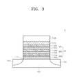
- FIG. 3 is a schematic view illustrating a ferroelectric memory device according to an embodiment of the present disclosure
- FIG. 4 is a schematic view illustrating a ferroelectric memory device according to an embodiment of the present disclosure.
- FIG. 5 is a flow chart schematically illustrating a method of manufacturing a ferroelectric memory device according to an embodiment of the present disclosure.
- FIGS. 6 to 10 are schematic views illustrating a method of manufacturing a ferroelectric memory device according to an embodiment of the present disclosure.
- first element is referred to as located on a second element, it may be understood that the first element is directly located on the second element; that an additional element may be interposed between the first element and the second element; or that a portion of the first element is directly located on a portion of the second element.
- first element is referred to as located on a second element, it may be understood that the first element is directly located on the second element; that an additional element may be interposed between the first element and the second element; or that a portion of the first element is directly located on a portion of the second element.
- the same reference numerals may refer to the same elements throughout the specification.
- each step or process in a method or manufacturing method disclosed herein may be performed sequentially in the stated order, may be performed out of sequence from the stated order, or may be performed substantially at the same time as one or more other steps or processes.
- the steps or processes may also be performed in a reverse order.
- An embodiment of the present disclosure includes a ferroelectric memory device having a ferroelectric superlattice structure.
- Techniques for developing or inducing ferroelectric properties in paraelectric materials have been reported in recent research. As an example, it has been reported that, in a thin film fabricating process, when anisotropic stress is applied to a thin non-ferroelectric hafnium oxide film, a lattice structure is transformed from a tetragonal crystal system to an orthorhombic crystal system, forming a hafnium oxide layer having ferroelectric properties.
- anisotropic stress may be produced through doping with dopants, surface energy effects, and thin film growth mechanisms in relation to a hafnium oxide layer. J. Müller, et al.
- Hf x Zr y O 2 (0 ⁇ x, y ⁇ 1) including hafnium oxide (HfO 2 ) and zirconium oxide (ZrO 2 )
- Hf x Zr y O 2 when the content ratio of hafnium (Hf) and zirconium (Zr) constituting the hafnium oxide (HfO 2 ) and the zirconium oxide (ZrO 2 ) is controlled, the Hf x Zr y O 2 solid solution can have a structure of four-crystal system that has ferroelectric properties.
- a superlattice structure having two or more kinds of different dielectric layers that are alternately stacked or layered on a substrate.
- a first dielectric layer having a first composition may be disposed on a substrate, followed by a first dielectric layer having a second composition.
- a second dielectric layer having a first composition may be disposed on the first dielectric layer having a second composition, followed by a second dielectric layer having a second composition.
- Additional dielectric layers may be sequentially disposed on previously disposed dielectric layers consistent with this alternating pattern to form a superlattice structure.
- one or more unit-stacks may be used in a superlattice structure.
- lattice strain in portions of interface regions between dielectric layers with different compositions may be controlled by controlling the number of or the thickness of dielectric layers.
- the ferroelectric properties of the superlattice structure can be controlled through development of anisotropic stress in the interface regions.
- FIG. 1 is a schematic view illustrating a ferroelectric memory device according to an embodiment of the present disclosure.
- the ferroelectric memory device 1 may include a substrate 101 having a source region 102 and a drain region 103 .
- ferroelectric memory device 1 may include a superlattice structure 10 and a gate electrode layer 155 that are disposed over substrate 101 .
- the ferroelectric memory device 1 of this embodiment may be a nonvolatile memory device such as a transistor.
- Substrate 101 may comprise a semiconductor material.
- substrate 101 may comprise a silicon (Si) substrate, a gallium arsenide (GaAs) substrate, an indium phosphide (InP) substrate, a germanium (Ge) substrate, or a silicon germanium (SiGe) substrate.
- substrate 101 may be doped with n-type or p-type dopants to have conductivity.
- Source region 102 and drain region 103 may be doped with n-type or p-type dopants. In an embodiment, when substrate 101 is n-type doped, source region 102 and drain region 103 may be p-type doped. In another embodiment, when substrate 101 is p-type doped, source region 102 and drain region 103 may be n-type doped.
- An interfacial insulation layer 115 may be disposed between substrate 101 and superlattice structure 10 .
- Interfacial insulation layer 115 may form stable interfaces with each of the substrate 101 and superlattice structure 10 such that interfacial insulation layer 115 suppresses interfacial defects generated at an interface when substrate 101 directly contacts a dielectric layer 125 of superlattice structure 10 .
- the interfacial defects may deteriorate an insulation property between the substrate 101 and superlattice structure 10 .
- interfacial insulation layer 115 may have a lattice constant that is between the lattice constant of substrate 101 and the lattice constant of superlattice structure 10 .
- interfacial insulation layer 115 can suppress material diffusion between substrate 101 and superlattice structure 10 .
- Interfacial insulation layer 115 may be comprised of silicon oxide, silicon nitride, or silicon oxynitride as non-limiting examples.
- Interfacial insulation layer 115 may have an amorphous state.
- Superlattice structure 10 may include at least two kinds of different dielectric layers that are alternately stacked or layered. In an embodiment, each of the at least two kinds of different dielectric layers may have a ferroelectric characteristic before each layer is included in superlattice structure 10 . In another embodiment, each of the at least two kinds of different dielectric layers may not have a ferroelectric characteristic before each layer is included in ferroelectric superlattice structure 10 .
- superlattice structure 10 may include dielectric layers 125 a , 125 b 125 c , 135 a , 135 b and 135 c .
- Dielectric layers 125 a , 125 b and 125 c may comprise hafnium oxide, and dielectric layers 135 a , 135 b and 135 c may comprise zirconium oxide.
- hafnium oxide layers 125 a , 125 b and 125 c and zirconium oxide layers 135 a , 135 b and 135 c may be un-doped.
- hafnium oxide layers 125 a , 125 b and 125 c and zirconium oxide layers 135 a , 135 b and 135 c may each comprise, as dopants, carbon (C), silicon (Si), magnesium (Mg), aluminum (Al), yttrium (Y), nitrogen (N), germanium (Ge), tin (Sn), strontium (Sr), lead (Pb), calcium (Ca), barium (Ba), titanium (Ti), zirconium (Zr), gadolinium (Gd), or a combination of two or more thereof, by way of non-limiting examples.
- superlattice structure 10 may include a plurality of unit-stacks 10 a , 10 b and 10 c .
- Unit-stack 10 a may include one hafnium oxide layer 125 a and one zirconium oxide layer 135 a .
- unit-stack 10 b may include one hafnium oxide layer 125 b and one zirconium oxide layer 135 b
- unit-stack 10 c may include one hafnium oxide layer 125 c and one zirconium oxide layer 135 c .
- superlattice structure 10 may include three unit-stack structures 10 a , 10 b and 10 c , with one unit-stack structure disposed on interfacial insulation layer 115 and the remaining unit-stack structures disposed such that the hafnium oxide layers 125 a , 125 b and 125 c alternate with zirconium oxide layers 135 a , 135 b and 135 c .
- the number of unit-stacks may not be limited to be three.
- two or more unit-stacks may be included in the superlattice structure, with dielectric layers having a first composition disposed between, or alternatingly layered between, dielectric layers having a second composition.
- each of the hafnium oxide layers 125 a , 125 b and 125 c and each of the zirconium oxide layers 135 a , 135 b and 135 c may be a monolayer having a thickness of about five angstroms (5 ⁇ ).
- each of the hafnium oxide layers 125 a , 125 b and 125 c and each of the zirconium oxide layers 135 a , 135 b and 135 c may include a plurality of monolayers, with each monolayer having a thickness of about 5 ⁇ .
- superlattice structure 10 may have an entire thickness of about five to twenty nanometers (5 to 20 nm). Accordingly, the number of unit-stacks constituting superlattice structure 10 may be varied to achieve a thickness of about 5 to 20 nm, or to achieve a different thickness. Alternatively, the thicknesses of hafnium oxide layers 125 a , 125 b and 125 c and zirconium oxide layers 135 a , 135 b and 135 c may be individually varied to achieve a total thickness of superlattice structure 10 of about 5 to 20 nm, or to achieve a different thickness.
- hafnium oxide layers 125 a , 125 b and 125 c and zirconium oxide layers 135 a , 135 b and 135 c may each have the same thickness. In a further embodiment, hafnium oxide layers 125 a , 125 b and 125 c and zirconium oxide layers 135 a , 135 b and 135 c may each have the same number of monolayers.
- the uppermost layer of superlattice structure 10 may be zirconium oxide layer 135 c , on which depolarization suppressing layer 145 is disposed. Also, the lowest layer of superlattice structure 10 disposed on substrate 101 and interfacial insulation layer 115 may be hafnium oxide layer 125 a , which may interface with the interfacial insulation layer 115 .
- a depolarization suppressing layer 145 may be disposed between superlattice structure 10 and gate electrode layer 155 .
- a depolarization phenomenon may occur in an interface region of the different materials.
- the depolarization phenomenon means that the ferroelectricity of the ferroelectric material is lowered or diminished at an interface region between the ferroelectric material and the conductor.
- the depolarization phenomenon may degrade fatigue characteristics of the ferroelectric material when switching operations for remanent polarization of the ferroelectric material is repeatedly performed.
- depolarization suppressing layer 145 is disposed between superlattice structure 10 and gate electrode layer 155 to prevent the ferroelectric properties of the ferroelectric superlattice structure 10 from deteriorating.
- Depolarization suppressing layer 145 may include an electrical insulator.
- depolarization suppressing layer 145 may have a high-k dielectric constant such that polarization deterioration from repeated switching operations may be suppressed at an interface between superlattice structure 10 and depolarization suppressing layer 145 .
- a depolarization suppressing layer 145 having a high-k dielectric constant may include a zirconium oxide layer.
- a depolarization suppressing layer 145 having a high-k dielectric constant may include an aluminum oxide layer.
- gate electrode layer 155 may be disposed on depolarization suppressing layer 145 .
- Gate electrode layer 155 may include, without limitation, metal, conductive metal nitride, conductive metal oxide, or conductive metal carbide.
- gate electrode layer 155 may include tungsten (W), titanium (Ti), copper (Cu), aluminum (Al), ruthenium (Ru), tungsten nitride, titanium nitride, tantalum nitride, tungsten carbide, titanium carbide, tungsten silicide, titanium silicide, tantalum silicide, ruthenium oxide, or a combination of two or more thereof, by way of non-limiting examples.
- the ferroelectric memory device described above is capable of forming polarization having different polarities in a ferroelectric superlattice structure 10 .
- the formed polarization may be stored in a non-volatile manner in ferroelectric superlattice structure 10 .
- the stored polarization with different polarities may change the density of a carrier in a channel region formed in substrate 101 under interfacial insulation layer 115 when a reading voltage is applied to gate electrode layer 155 . According to the density of the carrier, working current conducting through the channel region is differentiated, so that electrical information stored in the ferroelectric memory device can be identified.
- superlattice structure 10 may include combinations of dielectric layers comprising different material structures.
- a dielectric layer may be selected from materials having a crystal structure in which atoms in a unit lattice can move to an asymmetric position with respect to each other in response to an externally applied stress.
- the material of a dielectric layer may have a crystal structure consistent with a tetragonal crystal system, a monoclinic crystal system, or a cubic crystal system, each of which is easily converted into an orthorhombic crystal system exhibiting ferroelectricity.
- dielectric layers in a unit-stack may comprise metal oxides having similar atomic sizes.
- a superlattice structure in which different dielectric layers such as a hafnium oxide layer and a zirconium oxide layer are alternately stacked on a substrate is disclosed.
- lattice strain in the interface region between dielectric layers of different compositions in the superlattice structure can be effectively increased as the thickness of dielectric layers is reduced, including for example reduction of a thickness to a monolayer.
- ferroelectric properties of the superlattice structure can be controlled by anisotropic stress generated in the interface regions having the lattice strain of the dielectric layers constituting the superlattice structure.
- FIG. 2 is a schematic view illustrating a ferroelectric memory device according to an embodiment of the present disclosure.
- ferroelectric memory device 2 has substantially the same configuration as ferroelectric memory device 1 described above and with reference to FIG. 1 , except that depolarization suppressing layer 145 (illustrated in FIG. 1 ) is omitted between superlattice structure 10 and gate electrode layer 155 in ferroelectric memory device 2 .
- layer 135 c is a zirconium oxide layer that may be disposed as the uppermost layer of superlattice structure 10 and unit-stack 10 c .
- Zirconium oxide layer 135 c may directly contact gate electrode layer 155 and may function as a depolarization suppressing layer for superlattice structure 10 .
- the number of unit-stacks may not be fixed at three.
- one or more unit-stacks may be included in the superlattice structure. Additional unit-stacks may be oriented such that, within the superlattice structure, dielectric layers with a first composition are disposed between dielectric layers with a second composition and dielectric layers with a second composition are disposed between dielectric layers with a first composition, or such that, within the superlattice structure, dielectric layers with a first composition are alternated with dielectric layers with a second composition, with the orientation of the unit-stacks resulting in the disposition of gate electrode layer 155 on a zirconium oxide layer.
- layers 135 a , 135 b and 135 c are each comprised of zirconium oxide, however, the thickness of zirconium oxide layer 135 c of unit-stack structure 10 c may be greater than the thickness of each of zirconium oxide layers 135 a and 135 b of unit-stack structures 10 a and 10 b.
- the depolarization phenomenon occurring at an interface between gate electrode layer 155 and superlattice structure 10 can be effectively suppressed by disposing gate electrode layer 155 on zirconium oxide layer 135 c , which has a high-k dielectric constant, without introducing an additional depolarization suppressing layer.
- FIG. 3 is a schematic view illustrating a ferroelectric memory device according to an embodiment of the present disclosure.
- ferroelectric memory device 3 has substantially the same configuration as ferroelectric memory device 1 of the embodiment described above and with reference to FIG. 1 , except for the stacking order of the dielectric layers in superlattice structure 30 .
- superlattice structure 30 may include three unit-stack structures 30 a , 30 b and 30 c .
- Each of the unit-stack structures 30 a , 30 b and 30 c may comprise zirconium oxide layers 135 a , 135 b and 135 c respectively and hafnium oxide layers 125 a , 125 b and 125 c respectively.
- superlattice structure 30 may include three unit-stack structures 30 a , 30 b and 30 c , with one unit-stack structure disposed on interfacial insulation layer 115 and the remaining unit-stack structures disposed such that zirconium oxide layers 135 a , 135 b and 135 c alternate with hafnium oxide layers 125 a , 125 b and 125 c .
- the number of unit-stacks may not be fixed at three. In such embodiments, one or more unit-stacks may be included in the superlattice structure.
- Additional unit-stacks may be oriented such that, within the superlattice structure, dielectric layers with a first composition are disposed between dielectric layers with a second composition and dielectric layers with a second composition are disposed between dielectric layers with a first composition, or such that, within the superlattice structure, dielectric layers with a first composition are alternated with dielectric layers with a second composition, with the orientation of the unit-stacks resulting in the disposition a zirconium oxide layer on the substrate or interfacial insulation layer.
- the uppermost layer of superlattice structure 30 may be hafnium oxide layer 125 c , on which depolarization suppressing layer 145 is disposed.
- the lowest layer of superlattice structure 30 disposed on substrate 101 and interfacial insulation layer 115 may be zirconium oxide layer 135 a , which may interface with the interfacial insulation layer 115 . Accordingly, zirconium oxide layer 135 a may be the lowest layer of superlattice structure 30 to interface with interfacial insulation layer 115 and hafnium oxide layer 125 c may be the top layer of superlattice structure 30 .
- depolarization suppressing layer 145 may be disposed on hafnium oxide layer 125 c to prevent formation of a direct interface with gate electrode layer 155 .
- Depolarization suppressing layer 145 may include an electrical insulator having a high-k dielectric constant.
- depolarization suppressing layer 145 may comprise a zirconium oxide layer.
- depolarization suppressing layer 145 may comprise an aluminum oxide layer.
- FIG. 4 is a schematic view illustrating a ferroelectric memory device according to an embodiment of the present disclosure.
- ferroelectric memory device 4 has substantially the same configuration as ferroelectric memory device 2 of embodiments described above and with reference to FIG. 2 , except for the order of dielectric layers in superlattice structure 40 .
- superlattice structure 40 may include three unit-stack structures 40 a , 40 b and 40 c and a dielectric layer 135 d .
- Dielectric layer 135 d may comprise zirconium oxide.
- Each of the unit-stack structures 40 a , 40 b and 40 c may comprise zirconium oxide layers 135 a , 135 b and 135 c respectively and hafnium oxide layers 125 a , 125 b and 125 c respectively.
- superlattice structure 40 may include three unit-stack structures 40 a , 40 b and 40 c , with one unit-stack structure disposed on interfacial insulation layer 115 and the remaining unit-stack structures disposed such that zirconium oxide layers 135 a , 135 b and 135 c alternate with hafnium oxide layers 125 a , 125 b and 125 c .
- the number of unit-stacks may not be fixed at three. In such embodiments, one or more unit-stacks may be included in the superlattice structure.
- Additional unit-stacks may be oriented such that, within the superlattice structure, dielectric layers with a first composition are disposed between dielectric layers with a second composition and dielectric layers with a second composition are disposed between dielectric layers with a first composition, or such that, within the superlattice structure, dielectric layers with a first composition are alternated with dielectric layers with a second composition, with the orientation of the unit-stacks resulting in the disposition a zirconium oxide layer on the substrate or interfacial insulation layer.
- the uppermost layer of superlattice structure 40 may be hafnium oxide layer 125 c , on which zirconium oxide layer 135 d is disposed.
- the lowest layer of superlattice structure 40 disposed on substrate 101 and interfacial insulation layer 115 may be zirconium oxide layer 135 a , which may interface with the interfacial insulation layer 115 .
- zirconium oxide layer 135 a may be the lowest layer of superlattice structure 40 to interface with interfacial insulation layer 115 and zirconium oxide layer 135 d may be the top layer of superlattice structure 40 .
- hafnium oxide layer 125 c may be the uppermost layer of superlattice structure 40 .
- hafnium oxide layer 125 c may directly interface with gate electrode layer 155 , resulting in depolarization of hafnium oxide layer 125 c.
- zirconium oxide layer 135 d is additionally formed on unit-stack structure 40 c as an uppermost layer of superlattice structure 40 so that zirconium oxide layer 135 d can form an interface directly with gate electrode layer 155 .
- zirconium oxide layer 135 d provides more electrical insulation and more interface stability with respect to gate electrode layer 155 . In this manner, any depolarization phenomenon occurring at the interface between gate electrode layer 155 and superlattice structure 40 can be effectively suppressed without introducing an additional depolarization suppressing layer.
- zirconium oxide layers 135 a , 135 b , 135 c and 135 d may each have substantially the same thickness.
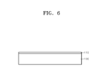
- FIG. 5 is a flow chart schematically illustrating a method of manufacturing a ferroelectric memory device according to an embodiment of the present disclosure.
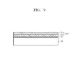
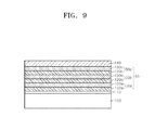
- FIGS. 6 to 10 are cross-sectional views schematically illustrating a method of manufacturing a ferroelectric memory device according to an embodiment of the present disclosure. Steps and processes disclosed herein and illustrated in FIGS. 5 to 10 may describe a manufacturing method of an embodiment of ferroelectric memory device 1 described above and with reference to FIG. 1 .
- Substrate 100 may comprise a silicon (Si) substrate, a gallium arsenide (GaAs) substrate, an indium phosphide (InP) substrate, a germanium (Ge) substrate, or a silicon germanium (SiGe) substrate by way of non-limiting examples.
- Substrate 100 may be doped with n-type or p-type dopants to have conductivity.
- a source region and a drain region may be formed in substrate 100 .
- the source region and the drain region may be doped with dopants of an opposite doping type to substrate 100 .
- the source region and the drain region may be p-type doped.
- the source region and the drain region may be n-type doped.
- the source region and the drain region may be formed in an upper portion of substrate 100 .
- the source region and the drain region may each be in the form of a well and created, for example, by ion implantation methods known in the art.
- interfacial insulation layer 110 is formed on an upper portion of substrate 100 and may compensate for the difference in lattice constant between a superlattice structure 50 that will be formed on interfacial insulation layer 110 and substrate 100 to eliminate, reduce or control interfacial stress.
- interfacial insulation layer 110 may have a lattice constant that is between the lattice constant of substrate 100 and the lattice constant of superlattice structure 50 .
- interfacial insulation layer 110 can serve as a barrier to material diffusion between substrate 100 and superlattice structure 50 .
- Interfacial insulation layer 110 may include, as non-limiting examples, a silicon oxide material, a silicon nitride material, or a silicon oxynitride material. Interfacial insulation layer 110 may be formed by, for example, applying a chemical vapor deposition method, an atomic layer deposition method, a coating method or other methods known in the art.
- a first dielectric layer having a first composition may be formed on a substrate, followed by a first dielectric layer having a second composition.
- a second dielectric layer having a first composition may be formed on the first dielectric layer having a second composition, followed by a second dielectric layer having a second composition.
- Additional dielectric layers may be sequentially formed on previously formed dielectric layers consistent with this alternating pattern to form a superlattice structure.
- one or more unit-stacks may be used in a superlattice structure.
- a unit-stack may comprise a dielectric layer with a first composition, followed by a dielectric layer with a second, different composition formed on the dielectric layer with a first composition.
- Additional unit-stacks in a superlattice structure may be oriented such that, within the superlattice structure, dielectric layers with a first composition are formed between dielectric layers with a second composition and dielectric layers with a second composition are formed between dielectric layers with a first composition, or such that, within the superlattice structure, dielectric layers with a first composition are alternated with dielectric layers with a second composition.
- first hafnium oxide layer 120 a and a first zirconium oxide layer 130 a are sequentially formed on interfacial insulation layer 110 .
- First hafnium oxide layer 120 a and first zirconium oxide layer 130 a may form a first unit-stack structure 50 a .
- First hafnium oxide layer 120 a and first zirconium oxide layer 130 a may be formed by utilizing, for example, an atomic layer deposition method, a chemical vapor deposition method, a molecular beam evaporation method, an evaporation method or other methods known in the art.
- first hafnium oxide layer 120 a is formed as a monolayer of about 5 ⁇ thick on interfacial insulation layer 110 , and then first zirconium oxide layer 130 a is formed on first hafnium oxide layer 120 a as a monolayer of about 5 ⁇ thick.
- first hafnium oxide layer 120 a is formed by disposing a plurality of monolayers of hafnium oxide on interfacial insulation layer 110 , and then first zirconium oxide layer 130 a is formed by disposing a plurality of monolayers of zirconium oxide on first hafnium oxide layer 120 a .
- the thickness of first hafnium oxide layer 120 a and the thickness of first zirconium oxide layer 130 a may be substantially the same.
- first hafnium oxide layer 120 a and first zirconium oxide layer 130 a may be formed, for example, at a substrate temperature of about 150 degrees Celcius (° C.) to 350 degrees Celcius (° C.).
- First hafnium oxide layer 120 a and first zirconium oxide layer 130 a may be formed in an amorphous state, a partially crystalline state, or a fully crystalline state.
- a second unit-stack 50 b and a third unit-stack 50 c are sequentially formed on first unit-stack 50 a .
- Unit-stack 50 b includes a second hafnium oxide layer 120 b and a second zirconium oxide layer 130 b
- the third unit-stack structure 50 c includes a third hafnium oxide layer 120 c and a third zirconium oxide layer 130 c.
- the second and third unit-stack structures 50 b and 50 c may be formed using methods that are substantially the same as methods for forming first unit-stack structure 50 a .
- superlattice structure 50 may be formed with three unit-stack structures 50 a , 50 b and 50 c .
- superlattice structure 50 may be formed, for example, with a total thickness of about 5 to 20 nm.
- a depolarization suppressing layer 140 may be additionally formed on superlattice structure 50 .
- Depolarization suppressing layer 140 may, for example, include a zirconium oxide layer or an aluminum oxide layer.
- Depolarization suppressing layer 140 may, for example, be formed using a chemical vapor deposition method, an atomic layer deposition method, a coating method or similar methods known in the art.
- the process for forming the zirconium oxide layer may be performed in-situ during formation of superlattice structure 50 .
- the process for forming depolarization suppressing layer 140 may be performed ex-situ after forming the superlattice structure 50 .
- Gate electrode layer 150 is formed on depolarization suppressing layer 140 .
- Gate electrode layer 150 may include tungsten (W), titanium (Ti), copper (Cu), aluminum (Al), tungsten nitride, titanium nitride, tantalum nitride, tungsten carbide, titanium carbide, tungsten silicide, titanium silicide, tantalum silicide, ruthenium oxide or a combination of two or more thereof, as non-limiting examples.
- Gate electrode layer 150 may, for example, be formed using a sputtering method, a chemical vapor deposition method, an evaporation method or an atomic layer deposition method.
- a crystallization heat treatment for hafnium oxide layers 120 a , 120 b and 120 c and zirconium oxide layers 130 a , 130 b and 130 c may be additionally performed.
- the crystallization heat treatment may be performed at a process temperature of about 400° C. to 600° C.
- the crystallization heat treatment may be performed after forming gate electrode layer 150 . In another embodiment, the crystallization heat treatment may be performed before forming gate electrode layer 150 . In yet another embodiment, the crystallization heat treatment may be performed during formation of gate electrode layer 150 .
- hafnium oxide layers 120 a , 120 b and 120 c and zirconium oxide layers 130 a , 130 b and 130 c may crystallize during formation of gate electrode layer 150 , in which case the additional crystallization heat treatment may be omitted.
- gate electrode layer 150 and superlattice structure 50 may be patterned over substrate 100 to form a gate structure.
- a ferroelectric memory device including the gate structure, a channel region formed in substrate 100 under the gate structure, and a source region and a drain region disposed in the substrate of both sides of the gate structure can be fabricated.
- the source region and the drain region may be formed after forming the gate structure. The source region and the drain region may be formed by selectively doping substrate 100 using known ion implantation methods.
- the process of forming depolarization suppressing layer 140 described above with reference to FIGS. 5, 9 and 10 may be omitted. Accordingly, zirconium oxide layer 130 c , which is the uppermost layer of superlattice structure 50 , can perform the function of depolarization suppressing layer 140 .
- the thickness of zirconium oxide layer 130 c of the third unit-stack structure 50 c may be greater than the thickness of zirconium oxide layers 130 a and 130 b of the first and second unit-stack structures 50 a and 50 b respectively.
- unit-stacks 50 a , 50 b and 50 c in S 120 of FIG. 5 the order of hafnium oxide layers 120 a , 120 b and 120 c and zirconium oxide layers 130 a , 130 b and 130 c may be reversed within each unit-stack illustrated in FIGS. 7 to 10 . More specifically, in unit-stack structures 50 a , 50 b and 50 c , zirconium oxide layers 130 a , 130 b and 130 c may be formed in the lower portion of the respective unit-stack structures and hafnium oxide layers 120 a , 120 b and 120 c may be formed at the upper portions of each respective unit-stack.
- the zirconium oxide layer may be formed closer to substrate 100 relative to the hafnium oxide layer, which is in turn formed closer to gate electrode 150 relative to the zirconium oxide layer.
- an additional zirconium oxide layer may be formed on hafnium oxide layer 120 c in the process of forming superlattice structure 50 .
- a superlattice structure including at least two kinds of different dielectric layers alternately stacked or layered is formed on a substrate.
- the stress generated at an interface between the different dielectric layers in the formation of the superlattice structure can convert the superlattice structure into a ferroelectric structure.
- a structurally stable ferroelectric material layer can be provided by effectively increasing lattice strain in the interfacial region and controlling anisotropic stress in the interfacial region having the increased lattice strain.
Landscapes
- Engineering & Computer Science (AREA)
- Microelectronics & Electronic Packaging (AREA)
- Power Engineering (AREA)
- Physics & Mathematics (AREA)
- Condensed Matter Physics & Semiconductors (AREA)
- General Physics & Mathematics (AREA)
- Computer Hardware Design (AREA)
- Ceramic Engineering (AREA)
- Manufacturing & Machinery (AREA)
- Chemical & Material Sciences (AREA)
- Crystallography & Structural Chemistry (AREA)
- Nanotechnology (AREA)
- Composite Materials (AREA)
- Materials Engineering (AREA)
- Chemical Kinetics & Catalysis (AREA)
- General Chemical & Material Sciences (AREA)
- Semiconductor Memories (AREA)
- Non-Volatile Memory (AREA)
Applications Claiming Priority (2)
| Application Number | Priority Date | Filing Date | Title |
|---|---|---|---|
| KR10-2017-0024300 | 2017-02-23 | ||
| KR1020170024300A KR20180097377A (ko) | 2017-02-23 | 2017-02-23 | 강유전성 메모리 장치 및 그 제조 방법 |
Publications (2)
| Publication Number | Publication Date |
|---|---|
| US20180240804A1 US20180240804A1 (en) | 2018-08-23 |
| US10475813B2 true US10475813B2 (en) | 2019-11-12 |
Family
ID=63167979
Family Applications (1)
| Application Number | Title | Priority Date | Filing Date |
|---|---|---|---|
| US15/820,376 Active US10475813B2 (en) | 2017-02-23 | 2017-11-21 | Ferroelectric memory device and method of manufacturing the same |
Country Status (3)
| Country | Link |
|---|---|
| US (1) | US10475813B2 (zh) |
| KR (1) | KR20180097377A (zh) |
| CN (1) | CN108511517B (zh) |
Cited By (3)
| Publication number | Priority date | Publication date | Assignee | Title |
|---|---|---|---|---|
| US11469043B2 (en) * | 2017-08-30 | 2022-10-11 | Micron Technology, Inc. | Electronic device comprising conductive material and ferroelectric material |
| WO2022225698A3 (en) * | 2021-04-05 | 2022-11-24 | The Regents Of The University Of California | Superlattice, ferroic order thin films for use as high/negative-k dielectric |
| US11832449B2 (en) | 2020-05-14 | 2023-11-28 | Samsung Electronics Co., Ltd. | Semiconductor device |
Families Citing this family (23)
| Publication number | Priority date | Publication date | Assignee | Title |
|---|---|---|---|---|
| US20190245056A1 (en) * | 2018-02-02 | 2019-08-08 | International Business Machines Corporation | Ferroelectric devices free of extended grain boundaries |
| US11101362B2 (en) * | 2018-07-30 | 2021-08-24 | Taiwan Semiconductor Manufacturing Co., Ltd. | Semiconductor device and forming method thereof |
| US20200098926A1 (en) * | 2018-09-26 | 2020-03-26 | Intel Corporation | Transistors with ferroelectric gates |
| US11349008B2 (en) * | 2018-09-27 | 2022-05-31 | Taiwan Semiconductor Manufacturing Co., Ltd. | Negative capacitance transistor having a multilayer ferroelectric structure or a ferroelectric layer with a gradient doping profile |
| KR20200071852A (ko) * | 2018-12-04 | 2020-06-22 | 삼성전자주식회사 | 강유전층을 포함하는 전자 소자 |
| US20210384197A1 (en) * | 2019-06-14 | 2021-12-09 | Samsung Electronics Co., Ltd. | Semiconductor memory devices and methods of fabricating the same |
| JP7292140B2 (ja) * | 2019-07-25 | 2023-06-16 | ルネサスエレクトロニクス株式会社 | 半導体装置の製造方法 |
| US11895855B2 (en) * | 2019-08-29 | 2024-02-06 | Samsung Electronics Co., Ltd. | Light-emitting device |
| KR20210033346A (ko) * | 2019-09-18 | 2021-03-26 | 삼성전자주식회사 | 전자 소자 및 그 제조방법 |
| KR20210036714A (ko) * | 2019-09-26 | 2021-04-05 | 삼성전자주식회사 | 강유전 박막 구조체 및 그 제조방법과, 강유전 박막 구조체를 포함하는 전자 소자 |
| US11532355B2 (en) * | 2019-09-26 | 2022-12-20 | The Regents Of The University Of California | Non-volatile multi-level cell memory using a ferroelectric superlattice and related systems |
| US11139315B2 (en) * | 2019-10-31 | 2021-10-05 | Qualcomm Incorporated | Ferroelectric transistor |
| KR20210111625A (ko) * | 2020-03-03 | 2021-09-13 | 삼성전자주식회사 | 강유전 박막 구조체 및 이를 포함하는 전자 소자 |
| US11450370B2 (en) | 2020-06-19 | 2022-09-20 | Taiwan Semiconductor Manufacturing Company, Ltd. | Ferroelectric field-effect transistor (FeFET) memory |
| US11749718B2 (en) * | 2021-03-05 | 2023-09-05 | Taiwan Semiconductor Manufacturing Company, Ltd. | Semiconductor device and manufacturing method thereof |
| CN113571583A (zh) * | 2021-06-16 | 2021-10-29 | 西安电子科技大学 | 基于HfO2-ZrO2超晶格铁电栅介质的晶体管及其制备方法 |
| US11791383B2 (en) * | 2021-07-28 | 2023-10-17 | Infineon Technologies Ag | Semiconductor device having a ferroelectric gate stack |
| CN113725289A (zh) * | 2021-08-09 | 2021-11-30 | 西安电子科技大学 | 一种超晶格结构薄膜及其应用 |
| KR20230045291A (ko) * | 2021-09-28 | 2023-04-04 | 에스케이하이닉스 주식회사 | 반도체 장치 및 그 제조 방법 |
| CN114023876B (zh) * | 2021-10-29 | 2023-08-25 | 华中科技大学 | 一种基于HfO2/ZrO2或HfO2/Al2O3超晶格铁电忆阻器及其制备 |
| CN114284361B (zh) * | 2021-12-29 | 2023-03-24 | 湘潭大学 | 半导体存储器、铁电场效应晶体管和铁电薄膜电容器 |
| US11973123B2 (en) * | 2022-01-18 | 2024-04-30 | Sandisk Technologies Llc | Ferroelectric devices including a single crystalline ferroelectric layer and method of making the same |
| US20230292526A1 (en) * | 2022-03-11 | 2023-09-14 | Taiwan Semiconductor Manufacturing Company, Ltd. | Memory Device Structure and Manufacturing Method Thereof |
Citations (9)
| Publication number | Priority date | Publication date | Assignee | Title |
|---|---|---|---|---|
| US5789071A (en) * | 1992-11-09 | 1998-08-04 | Northwestern University | Multilayer oxide coatings |
| US20030152813A1 (en) * | 1992-10-23 | 2003-08-14 | Symetrix Corporation | Lanthanide series layered superlattice materials for integrated circuit appalications |
| US20040036111A1 (en) * | 2002-03-26 | 2004-02-26 | Matsushita Electric Industrial Co., Ltd. | Semiconductor device and a fabrication method thereof |
| US20070049051A1 (en) * | 2005-08-29 | 2007-03-01 | Micron Technology, Inc. | Atomic layer deposition of Zrx Hfy Sn1-x-y O2 films as high k gate dielectrics |
| US20090087623A1 (en) * | 2007-09-28 | 2009-04-02 | Brazier Mark R | Methods for the deposition of ternary oxide gate dielectrics and structures formed thereby |
| US20130244016A1 (en) | 2010-10-13 | 2013-09-19 | Minoru Osada | Ferroelectric thin film having superlattice structure, manufacturing method thereof, ferroelectric element, and manufacturing method thereof |
| KR20150005709A (ko) | 2012-06-05 | 2015-01-14 | 도꾸리쯔교세이호진 상교기쥬쯔 소고겡뀨죠 | 반도체 강유전체 기억 트랜지스터 및 그의 제조 방법 |
| US20170294219A1 (en) * | 2015-09-01 | 2017-10-12 | Micron Technology, Inc. | Methods of operating ferroelectric memory cells, and related ferroelectric memory cells and capacitors |
| US20180218911A1 (en) * | 2017-01-27 | 2018-08-02 | Applied Materials, Inc. | Modifying work function of a metal film with a plasma process |
Family Cites Families (3)
| Publication number | Priority date | Publication date | Assignee | Title |
|---|---|---|---|---|
| TWI255467B (en) * | 2004-06-25 | 2006-05-21 | Univ Tsinghua | Linear ferroelectric element with lead zirconate and barium zirconate supper lattice structure |
| KR100644405B1 (ko) * | 2005-03-31 | 2006-11-10 | 삼성전자주식회사 | 불휘발성 메모리 장치의 게이트 구조물 및 이의 제조 방법 |
| US20070158640A1 (en) * | 2005-12-22 | 2007-07-12 | Rj Mears, Llc | Electronic device including a poled superlattice having a net electrical dipole moment |
-
2017
- 2017-02-23 KR KR1020170024300A patent/KR20180097377A/ko not_active Application Discontinuation
- 2017-11-21 US US15/820,376 patent/US10475813B2/en active Active
- 2017-12-08 CN CN201711296456.7A patent/CN108511517B/zh active Active
Patent Citations (9)
| Publication number | Priority date | Publication date | Assignee | Title |
|---|---|---|---|---|
| US20030152813A1 (en) * | 1992-10-23 | 2003-08-14 | Symetrix Corporation | Lanthanide series layered superlattice materials for integrated circuit appalications |
| US5789071A (en) * | 1992-11-09 | 1998-08-04 | Northwestern University | Multilayer oxide coatings |
| US20040036111A1 (en) * | 2002-03-26 | 2004-02-26 | Matsushita Electric Industrial Co., Ltd. | Semiconductor device and a fabrication method thereof |
| US20070049051A1 (en) * | 2005-08-29 | 2007-03-01 | Micron Technology, Inc. | Atomic layer deposition of Zrx Hfy Sn1-x-y O2 films as high k gate dielectrics |
| US20090087623A1 (en) * | 2007-09-28 | 2009-04-02 | Brazier Mark R | Methods for the deposition of ternary oxide gate dielectrics and structures formed thereby |
| US20130244016A1 (en) | 2010-10-13 | 2013-09-19 | Minoru Osada | Ferroelectric thin film having superlattice structure, manufacturing method thereof, ferroelectric element, and manufacturing method thereof |
| KR20150005709A (ko) | 2012-06-05 | 2015-01-14 | 도꾸리쯔교세이호진 상교기쥬쯔 소고겡뀨죠 | 반도체 강유전체 기억 트랜지스터 및 그의 제조 방법 |
| US20170294219A1 (en) * | 2015-09-01 | 2017-10-12 | Micron Technology, Inc. | Methods of operating ferroelectric memory cells, and related ferroelectric memory cells and capacitors |
| US20180218911A1 (en) * | 2017-01-27 | 2018-08-02 | Applied Materials, Inc. | Modifying work function of a metal film with a plasma process |
Non-Patent Citations (1)
| Title |
|---|
| Okuyama et al., Ferroelectric Thin Films, Springer, pp. 1-4 (Retrieved through Google Books) (Year: 2005). * |
Cited By (3)
| Publication number | Priority date | Publication date | Assignee | Title |
|---|---|---|---|---|
| US11469043B2 (en) * | 2017-08-30 | 2022-10-11 | Micron Technology, Inc. | Electronic device comprising conductive material and ferroelectric material |
| US11832449B2 (en) | 2020-05-14 | 2023-11-28 | Samsung Electronics Co., Ltd. | Semiconductor device |
| WO2022225698A3 (en) * | 2021-04-05 | 2022-11-24 | The Regents Of The University Of California | Superlattice, ferroic order thin films for use as high/negative-k dielectric |
Also Published As
| Publication number | Publication date |
|---|---|
| CN108511517A (zh) | 2018-09-07 |
| CN108511517B (zh) | 2021-07-20 |
| KR20180097377A (ko) | 2018-08-31 |
| US20180240804A1 (en) | 2018-08-23 |
Similar Documents
| Publication | Publication Date | Title |
|---|---|---|
| US10475813B2 (en) | Ferroelectric memory device and method of manufacturing the same | |
| US10522564B2 (en) | Ferroelectric memory device and method of manufacturing the same | |
| US10374054B2 (en) | Ferroelectric memory devices | |
| US10600808B2 (en) | Ferroelectric memory cell for an integrated circuit | |
| US10923501B2 (en) | Ferroelectric memory device and method of manufacturing the same | |
| KR101973248B1 (ko) | 극성, 비대칭성, 및 비-중심-대칭성 강유전성 물질들, 그러한 물질들을 포함하는 메모리 셀들, 및 관련 디바이스들 및 방법들 | |
| US11848193B2 (en) | Ferroelectric semiconductor device and method of manufacturing the same | |
| US10763360B2 (en) | Ferroelectric memory device and method of manufacturing the same | |
| US10847541B2 (en) | Ferroelectric memory device and a method of manufacturing the same | |
| US10475653B2 (en) | Methods of fabricating ferroelectric memory devices | |
| US11758737B2 (en) | Ferroelectric memory device and method of forming the same | |
| KR102514952B1 (ko) | 비휘발성 메모리 소자 및 이를 포함하는 크로스 포인트 어레이 장치 | |
| US11737280B2 (en) | Wakeup free approach to improve the ferroelectricity of FeRAM using a stressor layer | |
| US20220293766A1 (en) | Semiconducting Ferroelectric Device | |
| KR102479391B1 (ko) | 분극 가능한 물질을 이용한 메모리 소자 | |
| US11818895B2 (en) | Semiconductor device including ferroelectric layer and metal particles embedded in metal-organic framework layer | |
| US20230099330A1 (en) | Semiconductor device including ferroelectric layer and insulation layer with metal particles and methods of manufacturing the same | |
| US20230200078A1 (en) | Ferroelectric Device | |
| TW202415250A (zh) | 半導體裝置 | |
| KR20240060480A (ko) | 강유전성 구조물에 반강유전성을 유도하기 위한 억제층 삽입 |
Legal Events
| Date | Code | Title | Description |
|---|---|---|---|
| AS | Assignment |
Owner name: SK HYNIX INC., KOREA, REPUBLIC OF Free format text: ASSIGNMENT OF ASSIGNORS INTEREST;ASSIGNOR:YOO, HYANGKEUN;REEL/FRAME:044195/0944 Effective date: 20171116 |
|
| FEPP | Fee payment procedure |
Free format text: ENTITY STATUS SET TO UNDISCOUNTED (ORIGINAL EVENT CODE: BIG.); ENTITY STATUS OF PATENT OWNER: LARGE ENTITY |
|
| STPP | Information on status: patent application and granting procedure in general |
Free format text: ADVISORY ACTION MAILED |
|
| STPP | Information on status: patent application and granting procedure in general |
Free format text: DOCKETED NEW CASE - READY FOR EXAMINATION |
|
| STPP | Information on status: patent application and granting procedure in general |
Free format text: NOTICE OF ALLOWANCE MAILED -- APPLICATION RECEIVED IN OFFICE OF PUBLICATIONS |
|
| STPP | Information on status: patent application and granting procedure in general |
Free format text: PUBLICATIONS -- ISSUE FEE PAYMENT RECEIVED |
|
| STCF | Information on status: patent grant |
Free format text: PATENTED CASE |
|
| MAFP | Maintenance fee payment |
Free format text: PAYMENT OF MAINTENANCE FEE, 4TH YEAR, LARGE ENTITY (ORIGINAL EVENT CODE: M1551); ENTITY STATUS OF PATENT OWNER: LARGE ENTITY Year of fee payment: 4 |