US10074774B2 - Micro-LED device - Google Patents
Micro-LED device Download PDFInfo
- Publication number
- US10074774B2 US10074774B2 US15/528,730 US201515528730A US10074774B2 US 10074774 B2 US10074774 B2 US 10074774B2 US 201515528730 A US201515528730 A US 201515528730A US 10074774 B2 US10074774 B2 US 10074774B2
- Authority
- US
- United States
- Prior art keywords
- μled
- light emitting
- light
- mesa structure
- emitting source
- Prior art date
- Legal status (The legal status is an assumption and is not a legal conclusion. Google has not performed a legal analysis and makes no representation as to the accuracy of the status listed.)
- Active
Links
Images


Classifications
-
- H01L33/24—
-
- H—ELECTRICITY
- H10—SEMICONDUCTOR DEVICES; ELECTRIC SOLID-STATE DEVICES NOT OTHERWISE PROVIDED FOR
- H10H—INORGANIC LIGHT-EMITTING SEMICONDUCTOR DEVICES HAVING POTENTIAL BARRIERS
- H10H20/00—Individual inorganic light-emitting semiconductor devices having potential barriers, e.g. light-emitting diodes [LED]
- H10H20/80—Constructional details
- H10H20/81—Bodies
- H10H20/819—Bodies characterised by their shape, e.g. curved or truncated substrates
- H10H20/821—Bodies characterised by their shape, e.g. curved or truncated substrates of the light-emitting regions, e.g. non-planar junctions
-
- H—ELECTRICITY
- H10—SEMICONDUCTOR DEVICES; ELECTRIC SOLID-STATE DEVICES NOT OTHERWISE PROVIDED FOR
- H10H—INORGANIC LIGHT-EMITTING SEMICONDUCTOR DEVICES HAVING POTENTIAL BARRIERS
- H10H20/00—Individual inorganic light-emitting semiconductor devices having potential barriers, e.g. light-emitting diodes [LED]
- H10H20/80—Constructional details
- H10H20/81—Bodies
- H10H20/819—Bodies characterised by their shape, e.g. curved or truncated substrates
- H10H20/82—Roughened surfaces, e.g. at the interface between epitaxial layers
-
- H01L27/156—
-
- H01L33/06—
-
- H01L33/10—
-
- H01L33/32—
-
- H01L33/58—
-
- H—ELECTRICITY
- H10—SEMICONDUCTOR DEVICES; ELECTRIC SOLID-STATE DEVICES NOT OTHERWISE PROVIDED FOR
- H10H—INORGANIC LIGHT-EMITTING SEMICONDUCTOR DEVICES HAVING POTENTIAL BARRIERS
- H10H20/00—Individual inorganic light-emitting semiconductor devices having potential barriers, e.g. light-emitting diodes [LED]
- H10H20/80—Constructional details
- H10H20/81—Bodies
- H10H20/811—Bodies having quantum effect structures or superlattices, e.g. tunnel junctions
- H10H20/812—Bodies having quantum effect structures or superlattices, e.g. tunnel junctions within the light-emitting regions, e.g. having quantum confinement structures
-
- H—ELECTRICITY
- H10—SEMICONDUCTOR DEVICES; ELECTRIC SOLID-STATE DEVICES NOT OTHERWISE PROVIDED FOR
- H10H—INORGANIC LIGHT-EMITTING SEMICONDUCTOR DEVICES HAVING POTENTIAL BARRIERS
- H10H20/00—Individual inorganic light-emitting semiconductor devices having potential barriers, e.g. light-emitting diodes [LED]
- H10H20/80—Constructional details
- H10H20/81—Bodies
- H10H20/814—Bodies having reflecting means, e.g. semiconductor Bragg reflectors
-
- H—ELECTRICITY
- H10—SEMICONDUCTOR DEVICES; ELECTRIC SOLID-STATE DEVICES NOT OTHERWISE PROVIDED FOR
- H10H—INORGANIC LIGHT-EMITTING SEMICONDUCTOR DEVICES HAVING POTENTIAL BARRIERS
- H10H20/00—Individual inorganic light-emitting semiconductor devices having potential barriers, e.g. light-emitting diodes [LED]
- H10H20/80—Constructional details
- H10H20/81—Bodies
- H10H20/819—Bodies characterised by their shape, e.g. curved or truncated substrates
-
- H—ELECTRICITY
- H10—SEMICONDUCTOR DEVICES; ELECTRIC SOLID-STATE DEVICES NOT OTHERWISE PROVIDED FOR
- H10H—INORGANIC LIGHT-EMITTING SEMICONDUCTOR DEVICES HAVING POTENTIAL BARRIERS
- H10H20/00—Individual inorganic light-emitting semiconductor devices having potential barriers, e.g. light-emitting diodes [LED]
- H10H20/80—Constructional details
- H10H20/81—Bodies
- H10H20/822—Materials of the light-emitting regions
- H10H20/824—Materials of the light-emitting regions comprising only Group III-V materials, e.g. GaP
- H10H20/825—Materials of the light-emitting regions comprising only Group III-V materials, e.g. GaP containing nitrogen, e.g. GaN
-
- H—ELECTRICITY
- H10—SEMICONDUCTOR DEVICES; ELECTRIC SOLID-STATE DEVICES NOT OTHERWISE PROVIDED FOR
- H10H—INORGANIC LIGHT-EMITTING SEMICONDUCTOR DEVICES HAVING POTENTIAL BARRIERS
- H10H20/00—Individual inorganic light-emitting semiconductor devices having potential barriers, e.g. light-emitting diodes [LED]
- H10H20/80—Constructional details
- H10H20/84—Coatings, e.g. passivation layers or antireflective coatings
- H10H20/841—Reflective coatings, e.g. dielectric Bragg reflectors
-
- H—ELECTRICITY
- H10—SEMICONDUCTOR DEVICES; ELECTRIC SOLID-STATE DEVICES NOT OTHERWISE PROVIDED FOR
- H10H—INORGANIC LIGHT-EMITTING SEMICONDUCTOR DEVICES HAVING POTENTIAL BARRIERS
- H10H20/00—Individual inorganic light-emitting semiconductor devices having potential barriers, e.g. light-emitting diodes [LED]
- H10H20/80—Constructional details
- H10H20/85—Packages
- H10H20/855—Optical field-shaping means, e.g. lenses
-
- H—ELECTRICITY
- H10—SEMICONDUCTOR DEVICES; ELECTRIC SOLID-STATE DEVICES NOT OTHERWISE PROVIDED FOR
- H10H—INORGANIC LIGHT-EMITTING SEMICONDUCTOR DEVICES HAVING POTENTIAL BARRIERS
- H10H29/00—Integrated devices, or assemblies of multiple devices, comprising at least one light-emitting semiconductor element covered by group H10H20/00
- H10H29/10—Integrated devices comprising at least one light-emitting semiconductor component covered by group H10H20/00
- H10H29/14—Integrated devices comprising at least one light-emitting semiconductor component covered by group H10H20/00 comprising multiple light-emitting semiconductor components
- H10H29/142—Two-dimensional arrangements, e.g. asymmetric LED layout
-
- H—ELECTRICITY
- H10—SEMICONDUCTOR DEVICES; ELECTRIC SOLID-STATE DEVICES NOT OTHERWISE PROVIDED FOR
- H10H—INORGANIC LIGHT-EMITTING SEMICONDUCTOR DEVICES HAVING POTENTIAL BARRIERS
- H10H20/00—Individual inorganic light-emitting semiconductor devices having potential barriers, e.g. light-emitting diodes [LED]
- H10H20/80—Constructional details
- H10H20/84—Coatings, e.g. passivation layers or antireflective coatings
Definitions
- the invention relates to micro-LED ( ⁇ LED) devices. More specifically, the invention relates to, but is not limited to, ⁇ LEDs having improved collimation of light output.
- ⁇ LEDs When compared to standard LED devices, ⁇ LEDs may provide advantages of increased extraction efficiency (EE) and a “quasi-collimated” light output, that is, a light output that is at least partially directional. These advantages may be achieved by the introduction of a parabolic mesa structure to the ⁇ LED, in which an active layer or light emitting layer sits. Light that is emitted from the light emitting layer is reflected from the internal surface of the mesa and out of the ⁇ LED from an emission surface opposed to the mesa. Such a ⁇ LED is shown in U.S. Pat. No. 7,518,149.
- a micro-LED, ⁇ LED comprising: a substantially parabolic mesa structure; a light emitting source within the mesa structure; and a primary emission surface on a side of the device opposed to a top of the mesa structure; wherein the mesa structure has an aspect ratio, defined by (H 2 *H 2 )/Ac, of less than 0.5, and the ⁇ LED further comprises a reflective surface located in a region from the light emitting source to the primary emission surface, wherein the reflective surface has a roughness, Ra, less than 500 nm.
- Reflective surface as used herein encompasses a surface of a ⁇ LED to air, but more broadly, may also encompass an interface between two mediums.
- a reflective surface may be a surface of a ⁇ LED between an emitting medium and another medium. The light may be partially or fully reflected depending on its incidence angle.
- the primary emission surface is the surface of the ⁇ LED from which the majority of light is emitted.
- the primary emission surface may be a surface of an epilayer.
- the primary emission surface may be polished to achieve the desired surface roughness.
- the epilayer abuts a substrate of a different material one or both of the primary emission surface and a surface of the substrate may have a surface roughness, Ra, less than 500 nm. Further, one or both of the primary emission surface and a surface of the substrate may be polished to achieve the desired surface roughness.
- the low aspect ratio is counterintuitive to the disclosure of the art, as is the low roughness of the reflective surface.
- the combination of these features allows parasitic rays emitted from the emission source to be internally reflected, thereby reducing the half angle (and increasing the collimation) of the ⁇ LED.
- Previous ⁇ LEDs select a high aspect ratio and/or a rough or shaped reflective and/or emission surface to enhance the extraction efficiency.
- a low roughness reflective surface and a low aspect ratio near-parabolic mesa are combined. These two parameters taken separately decrease the extraction efficiency, but it is demonstrated herein that, when combined, they provide a surprising effect of the enhancement of the light collimation.
- the reflective surface is the primary emission surface.
- the reflective surface has a roughness, Ra, of less than 300 nm.
- the reflective surface is an interface between a first material having a first refractive index and a second material having a second refractive index.
- the first material comprises an epilayer and the second material comprises a substrate upon which the ⁇ LED is fabricated.
- the ⁇ LED is formed from GaN on a sapphire substrate, and wherein the interface between two materials is the interface between the GaN and the sapphire substrate.
- the reflective surface has a roughness, Ra, less than 500 nm (and, in exemplary apparatus, less than 300 nm) in a region greater than or equal to a cross sectional area of a base of the mesa, and aligned with a central axis of the mesa.
- the region may be in a range from substantially equal to the cross sectional area of the base of the mesa to 1.5 times the cross sectional area of the base of the mesa.
- the aspect ratio of the mesa structure is less than 0.3.
- the mesa structure comprises a truncated top.
- the light emitting source is offset from a central axis of the mesa structure.
- the light emitting source is offset by a distance on one or both of perpendicular axes lying in a plane parallel to the primary emission surface.
- the offset distance in each of the perpendicular axes is in a range from 1 ⁇ m to 5 ⁇ m.
- the offset distance in each of the perpendicular axes is in a range from 10% to 50% of the total distance from the central axis to an edge of the mesa in each of the perpendicular axes.
- the light emitting source is configured to emit light anisotropically, such that the light is emitted from the light emitting source substantially in a direction perpendicular to the direction of emission of light from the ⁇ LED.
- the emission of light from the light emitting source is controlled using index guiding and/or dipole anisotropy.
- the ⁇ LED further comprises an additive layer applied to the primary emission surface, wherein the additive layer attenuates light incident thereon at a given angle and/or at above a given wavelength.
- the additive layer is a multi-level dielectric filter.
- the source occupancy of the light emitting source within a light emitting layer of the mesa structure is in a range from 20% to 50%.
- a micro-LED, ⁇ LED comprising: a substantially parabolic mesa structure; a light emitting source within the mesa structure; and a primary emission surface on a side of the device opposed to a top of the mesa structure; wherein the mesa structure has an aspect ratio defined by (H 2 *H 2 )/Ac less than 0.3.
- a micro-LED, ⁇ LED comprising: a substantially parabolic mesa structure; a light emitting source within the mesa structure; and a primary emission surface on a side of the device opposed to a top of the mesa structure; wherein the light emitting source is offset from a central axis of the mesa structure.
- a micro-LED, ⁇ LED comprising: a substantially parabolic mesa structure; a light emitting source within the mesa structure; and a primary emission surface on a side of the device opposed to a top of the mesa structure; wherein the light emitting source is configured to emit light anisotropically, such that light is emitted from the light emitting source substantially in a direction perpendicular to the direction of emission of light from the ⁇ LED.
- a micro-LED, ⁇ LED, cluster comprising a plurality of ⁇ LEDs according to any described above and formed on a common substrate.
- a display device comprising a plurality of ⁇ LEDs according to any described above.
- a micro-LED, ⁇ LED comprising: a substantially parabolic mesa structure; a light emitting source within the mesa structure; and a primary emission surface on a side of the device opposed to a top of the mesa structure; wherein light emitted from the light emitting source is anisotropic.
- the anisotropic nature of the light emitted from the light emitting source may be in a direction substantially parallel to the primary emission surface, substantially perpendicular to a primary direction of emission of the ⁇ LED or substantially in a plane of the light emitting source.
- the light emitted by the light emitting source may be guided and/or encouraged within the mesa structure in a direction substantially parallel to the primary emission surface, substantially perpendicular to a primary direction of emission of the ⁇ LED or substantially in a plane of the light emitting source.
- the light emitting source may be substantially planar. Further, the primary direction of emission of the ⁇ LED may be taken as a direction from a centre of the light emitting source and normal to the primary emission surface.
- the light emitting source may be configured to emit light weighted towards a direction substantially parallel to the primary emission surface, substantially perpendicular to a primary direction of emission of the ⁇ LED or substantially in a plane of the light emitting source.
- the weighting may result in at least 50% of the emitted light being emitted in a range from 30 degrees, 25 degrees, 20 degrees, 15 degrees or 10 degrees either side of a direction substantially parallel to the primary emission surface, substantially perpendicular to a primary direction of emission of the ⁇ LED or substantially in a plane of the light emitting source.
- the weighting may result in at least 40%, 50%, 60% or 70% of the emitted light being directly incident on an internal sidewall of the mesa structure.
- the anisotropic light emitting source may form part of the guiding or may aid the guiding. That is, the guiding may be provided, at least in part, by the anisotropic emission of light from the light emitting source, or the guiding may be provided by configuration of a material within the mesa and aided by the anisotropic emission of light from the light emitting source.
- FIG. 1 is a section through a ⁇ LED
- FIGS. 2 a and 2 b are sections through ⁇ LEDs with mesa structures having different aspect ratios
- FIGS. 3 a and 3 b present the impact of aspect ratio variation over the half-angle and the extraction efficiency
- FIGS. 4 a and 4 b are sections through ⁇ LEDs with an unpolished (rough) primary emission surface and a polished (relatively less rough) primary emission surface;
- FIG. 5 shows the decrease in half angle of light emitted by a ⁇ LED due to reduction in roughness of a reflective surface of the ⁇ LED
- FIGS. 6 a and 6 b are sections through ⁇ LEDs with a centrally aligned emission source and an offset emission source;
- FIGS. 7 a and 7 b are plan views of ⁇ LEDs with a centrally aligned emission source and an offset emission source;
- FIG. 8 shows the effect of P contact misalignment on EE in a ⁇ LED
- FIG. 9 shows a polar plot of a modelled ⁇ LED with a light emitting source offset from the central axis of the mesa structure by 30%, 30%;
- FIGS. 10 a and 10 b show ⁇ LEDs having isotropic and anisotropic light emitting sources
- FIG. 11 shows a plot of transmission through a multi-layer dielectric filter applied as an additive layer to a ⁇ LED with an emission half-angle of 20° and a typical planar LED with a lambertian profile;
- FIG. 12 presents the power against current characteristics for processed ⁇ LEDs
- FIG. 13 shows the EE of ⁇ LEDs with various source occupancies
- FIG. 14 shows the influence of mesa aspect ratio and source occupancy on emission half angle.
- Exemplary ⁇ LEDs disclosed herein describe features for improving the collimation of the light generated by a ⁇ LED and extracted from the device to a surrounding medium. This may be done by allowing the reflection of the parasitic light rays back inside the substrate by using a low aspect ratio mesa combined with a reflective surface in a region from the mesa structure to the primary emission surface of the ⁇ LED.
- the reflective surface may be a polished primary emission surface or a reflective surface at a boundary between materials in the region from the mesa structure to the primary emission surface.
- the term “light” will be used in the sense that it is used in optical systems to mean not just visible light, but also electromagnetic radiation having a wavelength outside that of the visible range.
- the term “parasitic light rays” may refer to light rays emitted from a light emitting source at a point away from a focal point of a mesa structure within the ⁇ LED. Such parasitic light rays may be reflected from an internal surface of the mesa in a way that deflects them from the collimated output that is expected if light is emitted from the focal point.
- the term “low aspect ratio” encompasses mesa aspect ratios less than 0.5 and, in specific exemplary ⁇ LEDs, less than 0.3. This is explained in greater detail below.
- a ⁇ LED may also be operated as a photodiode. Any reference to a ⁇ LED made herein therefore also encompasses photodiodes.
- ⁇ LEDs should have a high aspect ratio mesa structure and a rough or shaped surface through which the light passes or is extracted to the surrounding medium. This is dominated by the view that a high EE is the most desirable feature of a ⁇ LED.
- ⁇ LEDs with a low aspect ratio mesa structure and a relatively higher reflectivity (e.g. polished) emission surface have improved collimation whilst maintaining a satisfactory EE.
- Improved collimation can be the most desirable feature of a ⁇ LED for multiple applications, including but not limited to electro-optical systems requiring stray light and light path management or a display, as detailed below.
- FIG. 1 shows a ⁇ LED 100 having a parabolic mesa structure in which the light emitting layer sits.
- FIG. 1 defines the parameters of the mesa structure in order to aid description of the ⁇ LEDs disclosed herein.
- a ⁇ LED 100 comprises, on a substrate 101 and a semiconductor layer 102 , a mesa 103 , a light emitting layer 104 , and an electrical contact 106 .
- an emission surface 108 of the ⁇ LED 100 is shown between the substrate 101 and the semiconductor 102 .
- the emission surface 108 may alternatively be defined as between the ⁇ LED 100 and the surrounding medium 110 , depending on the nature of the light emitting layer and the substrate.
- the ⁇ LED 100 comprises the following features and attributes:
- a further attribute of a ⁇ LED may defined as
- the mesa structure may or may not have a truncated top.
- H 3 is equal to H 4 .
- D 3 is equal to zero.
- H 1 can be less than, equal to or greater than H 2 , which respectively defines the cases when the focal point is above, in or below the LEL.
- D 1 can be less than, equal to or greater than D 2 depending on current spreading or current confinement in the material.
- FIG. 1 the size and dimensions of the features and attributes of FIG. 1 are exemplary and for the purposes of description and need not be indicative of the features and attributes of ⁇ LEDs 100 disclosed herein.
- An aspect ratio of a near parabolic mesa may be defined as (H 2 *H 2 )/Ac.
- the aspect ratio may also be defined as (H 3 *H 3 )/Ac in cases where the top of the mesa structure is truncated.
- the difference between an aspect ratio determined by (H 2 *H 2 )/Ac and one determined by (H 3 *H 3 )/Ac is negligible in many cases and (H 3 *H 3 )/Ac may be used as a proxy for the more accurate (H 2 *H 2 )/Ac.
- the determination of the aspect ratio does not require a mesa structure having a circular cross-section.
- the aspect ratio may also be determined for irregular mesa structures, e.g. mesa structures that are slightly deformed or elongated.
- Ac is determined by ⁇ *(D 4 /2)*(D 4 /2).
- FIGS. 2 a and 2 b show ⁇ LEDs having near parabolic mesa structures with different aspect ratios.
- FIG. 2 a shows a ⁇ LED 300 having a mesa structure with a relatively high aspect ratio
- FIG. 2 b shows a ⁇ LED 302 having a mesa structure with a relatively low aspect ratio.
- ⁇ LED 300 may have an aspect ratio of greater than or equal to 0.5
- ⁇ LED 302 may have an aspect ratio of less than 0.5 and, in particular exemplary case, the aspect ratio may be less than or equal to 0.3.
- ⁇ LEDs 300 , 302 have near-parabolic mesa structures 304 a , 304 b encapsulating light emitting sources 306 a , 306 b .
- the parabolic mesa structure may or may not have a truncated top that is the top of the parabola is flattened above the level of the light emitting source.
- the light emitted from the light emitting sources of the ⁇ LED devices 300 , 302 is considered to originate from a point source. However, the inventors have appreciated that this is not a true reflection of the way light is emitted from the light emitting sources 306 a , 306 b .
- the collimation of the light output from a ⁇ LED may be described using the inherent property of a parabola: that light originating from a point source at the focal point of the parabola is collimated into a parallel beam. Based on this and the analysis of ⁇ LEDs as emitting light from a point source, it has been assumed in known devices that using a high aspect ratio mesa allows a better collimation, as the mesa structure gets closer to a perfect, infinite parabola.
- the ⁇ LED 300 of FIG. 2 a has a near parabolic mesa structure with a high aspect ratio relative to the ⁇ LED 302 .
- the aspect ratio of the ⁇ LED 300 may be 0.5 or greater.
- light rays emitted from the light emitting layer 306 a that would be considered parasitic in ⁇ LED 302 are reflected from the internal surface of the mesa structure 304 a and, as such, are emitted from the primary emission surface 310 a instead of being internally reflected. This leads to enhanced extraction efficiency but reduced collimation of the output light, which, for many applications is an important parameter.
- the aspect ratio may be less than 0.5. In other exemplary ⁇ LEDs 302 , the aspect ratio may be less than 0.3. In other exemplary ⁇ LEDs 302 , the aspect ratio may be less than 0.2. In other exemplary ⁇ LEDs 302 , the aspect ratio may be less than 0.1. In other exemplary ⁇ LEDs 302 , the aspect ratio may be in a range from 0.1 to 0.25 or in a range from 0.01 to 0.25.
- the beam collimation of ⁇ LEDs may be increased by designing and processing the mesa structure to have an aspect ratio less than 0.5 and/or polishing the primary emission surface such that the surface roughness is reduced and the reflection properties are increased.
- the light emitting layer is encapsulated in a near-parabolic mesa structure.
- the light emitting layer may not be the same as the light emitting source.
- the light emitting layer defines the layer within the mesa structure in which the light emitting source sits.
- the light emitting layer may cover an area the same as the area of a cross section through the mesa structure at that level.
- the light emitting source may be the area of the light emitting layer that actually emits light.
- the light emitting source may be smaller than the light emitting layer.
- the mesa structure may have a low aspect ratio (typically H ⁇ H/Ac ⁇ 0.5), where H is the height of the mesa and Ac the light emitting layer area.
- the primary emission surface may be fully or partially polished or may be treated to allow internal reflection of angled rays.
- the combination of polished surface and low mesa aspect ratio allows the internal reflection of some unwanted parasitic rays, which have a large angle from the perpendicular of the primary emission surface and/or of the light emitting layer. If the primary emission surface is shaped (e.g., as a lens or other structure) the perpendicular to the primary emission surface cannot be so easily defined. In those cases the perpendicular may be defined as a perpendicular to the light emitting layer, or the axis of symmetry of the extracted beam. This allows enhancement of the emitted beam collimation.
- the light emitting source area is modelled as multiple sources or an extended source, near or in the plane of the mesa focal point. This plane may coincide with the light emitting layer.
- a percentage of parasitic rays are not reflected by the mesa structure, and thus propagated through the ⁇ LED directly to the primary emission surface, from which they are internally reflected.
- These parasitic rays can also be reflected by at an interface inside the material, for example at the interface GaN/Sapphire in case of a multi-material substrate or by a reflective coating layer between the substrate and the surrounding medium, or by any other reflective structures.
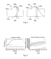
- FIGS. 3 a and 3 b present the impact of the H ⁇ H/Ac (aspect ratio) variation over the half-angle, which allows quantifying the collimation, ( FIG. 3 a ) and the extraction efficiency ( FIG. 3 b ) for a specific near parabolic mesa structure and source area.
- FIG. 3 a shows that aspect ratios below 0.5 show an unexpected decrease in half angle of the emitted beam, so an improvement of the light collimation. For different mesa structures and/or light emitting source areas, these results may change slightly.
- ⁇ LEDs relate to enhancement of the EE by increasing the aspect ratio of the mesa structure beyond 0.5.
- the extraction efficiency requires enhancement, but also the light collimation.
- EE can be sacrificed to some degree in favour of better collimation.
- Improvements in collimation of the light generated by a ⁇ LED and extracted from the device to the surrounding medium may be obtained by polishing the primary emission surface.
- a rough or a shaped emission surface is conventionally used in the LED industry in order to maximize the extraction efficiency, at the expense of collimation.
- a rough primary emission surface reduces internal reflection of light.
- polishing the primary emission surface allows an internal reflection of the parasitic light, which leads to an improved collimation.
- the roughness of the primary emission surface defined by Ra may be 500 nm or less, 150 nm or less, 100 nm or less or 50 nm or less.
- FIGS. 4 a and 4 b show ⁇ LEDs 500 , 502 with an unpolished (rough) primary emission surface 510 a and a polished (relatively less rough) primary emission surface 510 b .
- FIG. 4 a when the primary emission surface 510 a is unpolished, light rays 508 a that have not been reflected off an internal surface of the mesa structure 504 a interact with the primary emission surface 510 a and, due to the roughness, the angle at which the light rays 508 a are incident on the primary emission surface 510 a may be such that the light is emitted from the device 500 . This may increase EE, but it also increases the half-angle of the output light and so decreases collimation.
- the primary emission surface 510 b of the ⁇ LED 502 of FIG. 4 b has a polished primary emission surface 510 b , which is less rough than the primary emission surface 510 a . Therefore, the same light rays 508 b that were emitted by the device 500 are internally reflected. This may reduce the EE of the device but reduces the half-angle of the light output and so improves collimation.
- the half angle of the same micro-LEDs has been measured again.
- the results are plotted on FIG. 5 .
- a major improvement in beam collimation is observed when the primary emission surface is polished.
- a 20-40% improvement in beam collimation is observed for half angles below 25 degrees and a 5-20% improvement is observed for half angles above 25 degrees. This result highlights that the effect of polishing is more pronounced for a LED with naturally good collimation (i.e. a ⁇ LED).
- the interface at the surface determines the critical angle at which light is internally reflected.
- the reflective surface may be the primary emission surface, but in other exemplary ⁇ LEDs the reflective surface may be an interface surface between two materials.
- the interface may be provided by a single material that has a varying refractive index. In such ⁇ LEDs the refractive index of the material may continuously vary over an interface region. The wavelength of the emitted light may also affect the critical angle.
- Exemplary ⁇ LEDs may improve the collimation of the light generated by a micro-LED device and extracted from the device to the surrounding medium, by optimizing the position of the light emitting source in the mesa and taking advantage of the parasitic rays reflected back into the substrate (not extracted to the surrounding medium). That is, exemplary ⁇ LEDs may have a light emitting source that is offset from a central axis of the near parabolic mesa structure
- FIGS. 6 a and 6 b show the principal.
- FIG. 6 a shows ⁇ LEDs 700 , 702 with differently positioned light emitting sources 706 a , 706 b .
- the light emitting source 706 a is centralised with respect to a central axis running vertically through the mesa structure 704 a .
- the light emitting source 706 a may be circular.
- the light emitting source 706 a may be asymmetrical.
- the light source might be a ring around the centre with no emission at the centre (no emission at the focal plane).
- Light generated at the light emitting source 706 a is reflected off the internal walls of the mesa structure 704 a and emitted from the device 700 through the primary emission surface 710 a . It can be seen that light rays, such as 708 a , generated at the periphery of the light emitting source 706 a and/or contacting the lower edge of the mesa structure 704 a are emitted from the device 700 and provide the limit of the half-angle of the beam. In contrast, referring to FIG. 6 b , the light emitting source 706 b of the device 702 is offset from the central axis of the mesa structure 704 b .
- FIGS. 7 a and 7 b show plan views of the ⁇ LEDs 700 , 702 .
- the misalignment of the light emitting source 706 b is shown in FIG. 7 b .
- FIG. 7 a shows the light emitting source 706 a , which is aligned with the central axis of the mesa structure 704 a .
- Exemplary x offsets may be in the range from 1 to 5 ⁇ m or in a range from 0% to (D 4 ⁇ D 2 )/D 4 % of the radius of the light emitting layer.
- Exemplary y offsets may be in the range from 1 to 5 ⁇ m or in a range from 0% to (D 4 ⁇ D 2 )/D 4 % of the radius of the light emitting layer. Any combination of x and y offsets within those ranges is also possible. The x and y offsets may be in a range from 10% to 50% of the radius of the light emitting layer
- FIG. 9 shows a polar plot of a modelled ⁇ LED with a light emitting source offset from the central axis of the mesa structure by 30%, 30%.
- the collimation of light emitted from a ⁇ LED may also be improved by having an anisotropic light emitting source. That is, a light emitting source that emits light in only selected directions.
- An anisotropic source can enhance the collimation and extraction efficiency of a ⁇ LED by generating primarily those beam paths that are incident upon the near paraboloid mesa structure surface.
- source emission may be guided or encouraged perpendicular or primarily perpendicular to the device emission direction, that is, within the plane of the active layer of the ⁇ LED.
- the source emission may be guided substantially parallel to the primary emission surface of the ⁇ LED. It is counter-intuitive deliberately to guide light emission from a light emitting source in a plane perpendicular to the direction of the device emission, as typically light would be guided towards an emission surface.
- a source emission perpendicular or substantially perpendicular to the device emission direction coupled with a ⁇ LED mesa structure allows enhancing the extracted beam collimation and the extraction efficiency. If the source is isotropic then only a small proportion of the radiated light will be immediately incident upon the mesa internal reflective surface.
- FIGS. 10 a and 10 b show ⁇ LEDs 1100 , 1102 , which have isotropic and anisotropic light emitting sources respectively.
- FIG. 10 a shows light emitted from the light emitting source 1106 a in all directions.
- Only light rays 8 and 4 are immediately incident upon the mesa structure internal reflective surface. The remaining light rays mostly contribute to internal scattering and loss, reducing the extraction efficiency, or exit the surface without being guided by the mesa, broadening the collimated emitted beam.
- the light rays other than 8 and 4 are typically reflected from the planar top surface of the mesa 1104 a (light rays 1 and 3), not reflected by the mesa but propagated into the substrate (light rays 5 and 7) or coincidentally contribute to (but broaden) the collimated beam either directly (light ray 6) or after planar reflection (light ray 2).
- exemplary ⁇ LEDs more than 50% of the light emitted from the light emitting source is substantially perpendicular to the direction of emission, which may be defined by a normal to the light emitting layer. In other exemplary ⁇ LEDs, more than 80% of the light emitted from the light emitting source is substantially perpendicular to the direction of emission. In other exemplary ⁇ LEDs, more than 90% of the light emitted from the light emitting source is substantially perpendicular to the direction of emission.
- the proportion of the light rays that contribute to internal scattering may increase as the aspect ratio of the mesa structure is reduced and may negatively impact on the extraction efficiency of the ⁇ LED 1100 . Therefore to enhance extraction efficiency it is advantageous to eliminate parasitic light rays 1, 3, 5 and 7 by source anisotropy.
- the anisotropic light emitting source 1106 b shown in FIG. 10 b emits predominantly in the plane of the quantum wells of the light emitting source 1106 b .
- a greater proportion of the generated light is incident upon the inner reflective surface of the mesa structure 1104 b and a smaller proportion of generated light contributes to internal scattering and loss of the ⁇ LED.
- An anisotropic source may be created in several ways, not limited to the examples given below:
- an epitaxial structure is modulated with the quantum wells of the light emitting source 1106 b embedded in low refractive index material and higher refractive indices in outer cladding regions. This has the effect of guiding (bending) generated light back into the plane of the quantum wells.
- the quantum well emission may be isotropic but the index guiding of the cladding guides the light emitted from the light emitting source 1106 b to be away from loss paths, e.g. perpendicular to the direction of emission of the ⁇ LED 1102 .
- Dipole Anisotropy some semiconductor materials exhibit a spatial separation of electron and hole states, such that a dipole effect is apparent in certain planes.
- GaN has polar, semi-polar and non-polar planes. This spatial separation impacts the probability of recombination in certain polarisations which is linked to the direction of propagation. This can lead to enhanced photon emission in certain planes and suppressed photon emission in others, with the photons then exhibiting associated polarisation effects. This effect may be used to encourage light to be emitted from the light emitting source in a direction perpendicular to the direction of emission of the ⁇ LED 1102 .
- Exemplary ⁇ LEDs utilise refractive index guiding or crystal anisotropy effects to encourage propagation of light in the plane of the quantum wells.
- the anisotropic emission of light from the light emitting source may increase the extraction efficiency and/or the collimation of the light emitted from the ⁇ LED without the need to have a reflective region or low roughness surface in a range from the light emitting source to the primary emission surface.
- Collimation of the light generated by a ⁇ LED and extracted from the ⁇ LEDs to the surrounding medium may also be reduced by the application of additive layers on the primary emission surface.
- Additive layers applied to the primary emission surface may exhibit an angular dependence, that is, they may attenuate, reflect or propagate light incident on them based on the angle of incidence of the light. When applied to a ⁇ LED this effect may improve collimation by, for example, attenuating light incident on the additive layer at higher angles with respect to a normal to the primary emission surface. Conversely the transmission of the applied layer may be enhanced by application to a collimated source that matches the known angular dependence.
- Treatment of ⁇ LEDs on the primary emission surface may include the addition of layers with several alternative functions included but not limited to wavelength bandpass, high-pass, low-pass, reflecting or antireflecting filters.
- Such additive layers are known to have an angle of incidence (AOI) dependency that typically manifests as a loss mechanism when a filter is applied to a non-collimated device acting as a broad emission-angle source.
- AOI angle of incidence
- the primary function of these filters is not to affect a beam profile
- the AOI dependency means that as a secondary effect they can have beam shaping properties that enhance the functionality of the ⁇ LED by improving collimation, suppressing scattered light and reducing cross-talk in arrays of devices.
- the performance of these layers may be enhanced relative to non-collimated sources, as the associated loss of power at higher angles is greatly reduced when applied to a ⁇ LED.
- FIG. 11 shows a plot of transmission through a band pass filter applied as an additive layer to a ⁇ LED with an emission half-angle of 20° and a typical planar LED with a lambertian profile.
- the band pass filter heavily attenuates light incident on it at angles above 30°.
- the plot also shows the ratio of the ⁇ LED transmission and the planar LED transmission through the filter. It can be seen that at small angles of incidence the ⁇ LED delivers up to four times more power, and over the whole hemisphere the ⁇ LED delivers twice as much power as a planar device.
- the transmission loss through the filter is less for a ⁇ LED than when using a planar LED, as the application of a filter to a micro-LED yields a more efficient system.
- a multi-level dielectric filter may be used.
- the filter may have a pass band of 10 nm to 30 nm (in a particular example, 20 nm) and a nominal transmission wavelength anywhere in the visible region from 400 to 700 nm.
- Other proprietary filters can be applied from deep UV, through optical wavelengths to infra-red wavelength, with low-pass band-pass or high-pass properties that all display an angular dependence resulting in an improvement of ⁇ LED collimation.
- Light at angles of >10° from a normal to the light emitting layer experience attenuation effects and the majority of emission above 30° is not transmitted.
- More general types of additive layers are formed from multiple layers of dielectric film, each layer typically of the order ⁇ /4 thickness.
- Exemplary ⁇ LEDs disclosed herein may have improved wall-plug efficiency by designing the light emitting source area regarding the polished primary emission surface reflection properties.
- the light emitting source defined by its area, i.e. S area , is encapsulated in a near-parabolic mesa structure which may have a truncated top.
- the active layer also called the light emitting layer LEL, is defined by its area LEL area .
- the source occupancy is defined by the source area over the light emitting layer area: S area /LEL area .
- S area /LEL area For circular mesa, another way to define the source occupancy is D 2 *D 2 /(D 4 *D 4 ).
- the mesa may have a low aspect ratio (H 2 ⁇ H 2 /Ac ⁇ 0.5.
- the primary emission surface may be polished (or treated to allow internal reflection of angled rays).
- the wall plug efficiency is optimized while enlarging the source area
- U.S. Pat. No. 7,518,149 discloses a particularly high efficiency if the contact occupies less than 16% of the truncated top mesa surface area. This statement tends to indicate that more light is extracted from a ⁇ LED device when the source occupancy is reduced; i.e. that the wall plug efficiency is higher. Nevertheless, when the source occupancy is reduced, the contact is reduced and so the current density increases. So, for a same input power (I ⁇ V), depending on the IV characteristics of the material, more electrons can be injected through a large contact, and so more photons can be produced.
- I ⁇ V input power
- FIG. 12 presents the power vs current characteristics for processed ⁇ LEDs (GaN with NiAu contact).
- ⁇ LED for an input power of 0.5 mW: 90 ⁇ A can be injected for a source occupancy of 10%; and 98 ⁇ A can be injected for a source occupancy of 30%.
- the extraction efficiency may vary between the two designs due to the loss of collimation for a large source. For the specific mesa structure modelled, the extraction efficiency varies from: 48.2% for a source occupancy of 10% to 45.9% for a source occupancy of 30%.
- FIG. 13 shows the extraction efficiency (EE) of ⁇ LEDs with various source occupancies for a specific mesa design. Other designs (mesa aspect ratio, geometrical coefficients, . . . ) might bring slightly different results.
- the number of generated photons may increase by 9.2%, which, considering the loss due to the decrease of the extraction efficiency, still allows an overall increase of the wall plug efficiency of almost 4%.
- a low aspect ratio mesa structure (e.g. below 0.5) with a polished surface with low roughness for reflecting parasitic rays allows an improvement of the half angle of emitted light when compared to a high aspect ratio mesa structures. Enlarging the source occupancy increases the half-angle. So, for the same collimation requirement, a low aspect ratio mesa with an enlarged source occupancy can be used as shown in FIG. 14 .
- the mesa structure can be designed with a high aspect ratio (e.g., greater than 0.5) and a small source occupancy (e.g., 10% or less), or a low aspect ratio (e.g., less than 0.5) and a large source occupancy (e.g., greater than 50%).
- a high aspect ratio e.g., greater than 0.5
- a small source occupancy e.g., 10% or less
- a low aspect ratio e.g., less than 0.5
- a large source occupancy e.g., greater than 50%
- Enlarged source occupancies up to 100% can be utilised in real ⁇ LED applications and achieve acceptable levels of collimation when combined with low aspect ratio mesa structures.
- a high aspect ratio design with large source occupancy could result in unacceptable collimation. This allows trade-off of collimation with factors of forward voltage, manufacturability etc.
- Exemplary ⁇ LEDs disclosed herein provide advantages for stray light and light path management for electro-optical systems. Exemplary ⁇ LEDs simplify an optical system and packaging by removing bulk optics. In addition, exemplary ⁇ LEDs may remove background noise, reduce power requirement and/or reduce cross-talk between elements.
- exemplary ⁇ LEDs may: optimize the light coupling to the light-guide backplane; decrease the external losses; and/or enable different power savings backlighting architectures.
Landscapes
- Led Devices (AREA)
- Led Device Packages (AREA)
Applications Claiming Priority (3)
| Application Number | Priority Date | Filing Date | Title |
|---|---|---|---|
| GBGB1420860.7A GB201420860D0 (en) | 2014-11-24 | 2014-11-24 | Micro-LED device |
| GB1420860.7 | 2014-11-24 | ||
| PCT/EP2015/077332 WO2016083289A1 (en) | 2014-11-24 | 2015-11-23 | Micro-led device |
Related Parent Applications (1)
| Application Number | Title | Priority Date | Filing Date |
|---|---|---|---|
| PCT/EP2015/077332 A-371-Of-International WO2016083289A1 (en) | 2014-11-24 | 2015-11-23 | Micro-led device |
Related Child Applications (1)
| Application Number | Title | Priority Date | Filing Date |
|---|---|---|---|
| US16/103,853 Continuation US10490699B2 (en) | 2014-11-24 | 2018-08-14 | Micro-LED device |
Publications (2)
| Publication Number | Publication Date |
|---|---|
| US20170271557A1 US20170271557A1 (en) | 2017-09-21 |
| US10074774B2 true US10074774B2 (en) | 2018-09-11 |
Family
ID=52292442
Family Applications (3)
| Application Number | Title | Priority Date | Filing Date |
|---|---|---|---|
| US15/528,730 Active US10074774B2 (en) | 2014-11-24 | 2015-11-23 | Micro-LED device |
| US16/103,853 Active US10490699B2 (en) | 2014-11-24 | 2018-08-14 | Micro-LED device |
| US16/588,737 Active US10854782B2 (en) | 2014-11-24 | 2019-09-30 | Micro-LED device |
Family Applications After (2)
| Application Number | Title | Priority Date | Filing Date |
|---|---|---|---|
| US16/103,853 Active US10490699B2 (en) | 2014-11-24 | 2018-08-14 | Micro-LED device |
| US16/588,737 Active US10854782B2 (en) | 2014-11-24 | 2019-09-30 | Micro-LED device |
Country Status (7)
| Country | Link |
|---|---|
| US (3) | US10074774B2 (enExample) |
| EP (1) | EP3224873B1 (enExample) |
| JP (1) | JP6612869B2 (enExample) |
| KR (1) | KR102447697B1 (enExample) |
| CN (1) | CN107112388B (enExample) |
| GB (1) | GB201420860D0 (enExample) |
| WO (1) | WO2016083289A1 (enExample) |
Cited By (1)
| Publication number | Priority date | Publication date | Assignee | Title |
|---|---|---|---|---|
| US10490699B2 (en) * | 2014-11-24 | 2019-11-26 | Facebook Technologies, Llc | Micro-LED device |
Families Citing this family (36)
| Publication number | Priority date | Publication date | Assignee | Title |
|---|---|---|---|---|
| CN109983392B (zh) | 2016-12-09 | 2021-02-23 | 应用材料公司 | 准直led光场显示器 |
| US10490599B2 (en) * | 2017-07-13 | 2019-11-26 | Applied Materials, Inc. | Collimated, directional micro-LED light field display |
| US10712579B1 (en) * | 2017-09-20 | 2020-07-14 | Facebook Technologies, Llc | Vortex linearization of micro-LED polarization |
| US11238780B2 (en) | 2017-10-13 | 2022-02-01 | Hewlett-Packard Development Company, L.P. | Displays with movable privacy gates |
| US10720098B2 (en) * | 2017-11-15 | 2020-07-21 | Facebook Technologies, Llc | Pulse-width-modulation control of micro LED |
| US10468552B2 (en) * | 2018-03-30 | 2019-11-05 | Facebook Technologies, Llc | High-efficiency micro-LEDs |
| US10622519B2 (en) | 2018-03-30 | 2020-04-14 | Facebook Technologies, Llc | Reduction of surface recombination losses in micro-LEDs |
| JP7206628B2 (ja) * | 2018-04-27 | 2023-01-18 | セイコーエプソン株式会社 | 発光装置およびプロジェクター |
| EP3803976B1 (en) | 2018-05-24 | 2024-05-22 | Lumiode, Inc. | Led display structures and fabrication of same |
| US11145786B2 (en) | 2018-09-11 | 2021-10-12 | Facebook Technologies, Llc | Methods for wafer-to-wafer bonding |
| US11056611B2 (en) | 2018-09-11 | 2021-07-06 | Facebook Technologies, Llc | Mesa formation for wafer-to-wafer bonding |
| US11342479B2 (en) | 2018-09-11 | 2022-05-24 | Facebook Technologies, Llc | Reducing bowing of materials before wafer-to-wafer bonding for LED manufacturing |
| US11257982B1 (en) * | 2018-10-18 | 2022-02-22 | Facebook Technologies, Llc | Semiconductor display device |
| US11164905B2 (en) | 2018-10-18 | 2021-11-02 | Facebook Technologies, Llc | Manufacture of semiconductor display device |
| US11227970B1 (en) | 2018-10-18 | 2022-01-18 | Facebook Technologies, Llc | Light emitting diodes manufacture and assembly |
| EP3899920A4 (en) | 2018-12-21 | 2022-09-28 | Lumiode, Inc. | ADDRESSING FOR EMISSIVE INDICATORS |
| US11302248B2 (en) | 2019-01-29 | 2022-04-12 | Osram Opto Semiconductors Gmbh | U-led, u-led device, display and method for the same |
| US11271143B2 (en) | 2019-01-29 | 2022-03-08 | Osram Opto Semiconductors Gmbh | μ-LED, μ-LED device, display and method for the same |
| WO2020229576A2 (de) | 2019-05-14 | 2020-11-19 | Osram Opto Semiconductors Gmbh | Beleuchtungseinheit, verfahren zur herstellung einer beleuchtungseinheit, konverterelement für ein opto-elektronisches bauelement, strahlungsquelle mit einer led und einem konverterelement, auskoppelstruktur, und optoelektronische vorrichtung |
| CN121583214A (zh) | 2019-01-29 | 2026-02-27 | 奥斯兰姆奥普托半导体股份有限两合公司 | 视频墙、驱动器电路、控制系统及其方法 |
| KR20210120106A (ko) * | 2019-02-11 | 2021-10-06 | 오스람 옵토 세미컨덕터스 게엠베하 | 광전자 부품, 광전자 조립체 및 방법 |
| US11538852B2 (en) | 2019-04-23 | 2022-12-27 | Osram Opto Semiconductors Gmbh | μ-LED, μ-LED device, display and method for the same |
| JP7604394B2 (ja) | 2019-04-23 | 2024-12-23 | エイエムエス-オスラム インターナショナル ゲーエムベーハー | Ledモジュール、ledディスプレイモジュール、および当該モジュールを製造する方法 |
| KR102947058B1 (ko) | 2019-05-13 | 2026-04-01 | 에이엠에스-오스람 인터내셔널 게엠베하 | 다중 칩 캐리어 구조체 |
| WO2020233873A1 (de) | 2019-05-23 | 2020-11-26 | Osram Opto Semiconductors Gmbh | Beleuchtungsanordnung, lichtführungsanordnung und verfahren |
| US10840418B1 (en) * | 2019-05-28 | 2020-11-17 | Facebook Technologies, Llc | Fabricating parabolic-shaped LEDs |
| CN114730824A (zh) | 2019-09-20 | 2022-07-08 | 奥斯兰姆奥普托半导体股份有限两合公司 | 光电组件、半导体结构和方法 |
| US11309464B2 (en) | 2019-10-14 | 2022-04-19 | Facebook Technologies, Llc | Micro-LED design for chief ray walk-off compensation |
| GB2593181B (en) | 2020-03-17 | 2023-11-15 | Plessey Semiconductors Ltd | Micro-LED device |
| GB2593910B (en) | 2020-04-08 | 2022-09-28 | Plessey Semiconductors Ltd | Micro-lightguide for micro-LED |
| WO2021236652A1 (en) * | 2020-05-18 | 2021-11-25 | Avicenatech Corp. | Embedding leds with waveguides |
| GB2590744B (en) * | 2020-06-03 | 2022-02-02 | Plessey Semiconductors Ltd | Spacer micro-LED architecture for microdisplay applications |
| GB2595685B (en) * | 2020-06-03 | 2024-08-07 | Plessey Semiconductors Ltd | Spacer LED architecture for high efficiency micro LED displays |
| GB2595715B (en) | 2020-06-04 | 2022-08-17 | Plessey Semiconductors Ltd | Enhanced colour conversion and collimation of micro-LED devices |
| TWI779672B (zh) * | 2021-06-17 | 2022-10-01 | 錼創顯示科技股份有限公司 | 微型發光元件 |
| KR102854252B1 (ko) * | 2022-12-16 | 2025-09-04 | (재)한국나노기술원 | 고출력 발광소자의 제조방법 및 그에 의해 제조된 고출력 발광소자 |
Citations (11)
| Publication number | Priority date | Publication date | Assignee | Title |
|---|---|---|---|---|
| US20060113638A1 (en) * | 2003-05-02 | 2006-06-01 | Maaskant Pleun P | Light emitting diodes and the manufacture thereof |
| US20070210299A1 (en) * | 2006-03-08 | 2007-09-13 | Fujitsu Limited | Single-photon generating device, single-photon detecting device, and optical quantum gate |
| US20130175557A1 (en) * | 2011-09-02 | 2013-07-11 | The Procter & Gamble Company | Light emitting apparatus |
| US8507924B2 (en) * | 2004-07-02 | 2013-08-13 | Cree, Inc. | Light emitting diode with high aspect ratio submicron roughness for light extraction and methods of forming |
| WO2013121051A1 (en) | 2012-02-16 | 2013-08-22 | University College Cork, National University Of Ireland, Cork | Micro -led array with filters |
| GB201420860D0 (en) * | 2014-11-24 | 2015-01-07 | Infiniled Ltd | Micro-LED device |
| US9048409B2 (en) * | 2010-09-24 | 2015-06-02 | Seoul Semiconductor Co., Ltd. | Wafer-level light emitting diode package and method of fabricating the same |
| US20150236201A1 (en) * | 2012-09-03 | 2015-08-20 | Infiniled Limited | Optical device |
| US20150325746A1 (en) * | 2014-05-07 | 2015-11-12 | Infiniled Limited | Methods and apparatus for improving micro-led devices |
| WO2016122725A1 (en) * | 2015-01-30 | 2016-08-04 | Technologies Llc Sxaymiq | Micro-light emitting diode with metal side mirror |
| US9825200B2 (en) * | 2015-05-13 | 2017-11-21 | Au Optronics Corporation | Micro-light-emitting diode device and method for manufacturing the same |
Family Cites Families (22)
| Publication number | Priority date | Publication date | Assignee | Title |
|---|---|---|---|---|
| JP2005252086A (ja) * | 2004-03-05 | 2005-09-15 | Sony Corp | 半導体発光素子の製造方法、半導体発光素子、集積型半導体発光装置の製造方法、集積型半導体発光装置、画像表示装置の製造方法、画像表示装置、照明装置の製造方法および照明装置 |
| US6908219B1 (en) * | 2004-03-29 | 2005-06-21 | Valeo Sylvania Llc | Optical element for a high mounted stop lamp with an LED light source |
| US7750425B2 (en) * | 2005-12-16 | 2010-07-06 | The Trustees Of Princeton University | Intermediate-band photosensitive device with quantum dots embedded in energy fence barrier |
| US8434912B2 (en) * | 2006-02-27 | 2013-05-07 | Illumination Management Solutions, Inc. | LED device for wide beam generation |
| GB2456756A (en) * | 2008-01-16 | 2009-07-29 | Sharp Kk | AlInGaN Light-Emitting devices |
| JP2011512037A (ja) * | 2008-02-08 | 2011-04-14 | イルミテックス, インコーポレイテッド | エミッタ層成形のためのシステムおよび方法 |
| US20110012147A1 (en) * | 2009-07-15 | 2011-01-20 | Koninklijke Philips Electronics N.V. | Wavelength-converted semiconductor light emitting device including a filter and a scattering structure |
| KR101783955B1 (ko) * | 2011-02-10 | 2017-10-11 | 삼성디스플레이 주식회사 | 발광 다이오드 패키지 및 이를 구비한 백라이트 유닛 |
| WO2012150647A1 (ja) * | 2011-05-02 | 2012-11-08 | パナソニック株式会社 | スーパールミネッセントダイオード |
| DE102014009677A1 (de) * | 2014-02-19 | 2015-08-20 | Pierre-Alain Cotte | Anzeigevorrichtung mit verbessertem Kontrast |
| CN106463591A (zh) * | 2014-06-02 | 2017-02-22 | 3M创新有限公司 | 带有远程荧光粉和外壳反射器的led |
| US11437775B2 (en) * | 2015-08-19 | 2022-09-06 | Kyocera Sld Laser, Inc. | Integrated light source using a laser diode |
| KR20170043727A (ko) * | 2015-10-13 | 2017-04-24 | 삼성디스플레이 주식회사 | 표시 장치 |
| GB2544335A (en) * | 2015-11-13 | 2017-05-17 | Oculus Vr Llc | A method and apparatus for use in the manufacture of a display element |
| CN109983392B (zh) * | 2016-12-09 | 2021-02-23 | 应用材料公司 | 准直led光场显示器 |
| JP6910226B2 (ja) * | 2017-07-07 | 2021-07-28 | Hoya株式会社 | 光照射装置 |
| US10490599B2 (en) * | 2017-07-13 | 2019-11-26 | Applied Materials, Inc. | Collimated, directional micro-LED light field display |
| US10020422B1 (en) * | 2017-09-29 | 2018-07-10 | Oculus Vr, Llc | Mesa shaped micro light emitting diode with bottom N-contact |
| US10720098B2 (en) * | 2017-11-15 | 2020-07-21 | Facebook Technologies, Llc | Pulse-width-modulation control of micro LED |
| US10325791B1 (en) * | 2017-12-13 | 2019-06-18 | Facebook Technologies, Llc | Formation of elastomeric layer on selective regions of light emitting device |
| US10326052B1 (en) * | 2018-02-12 | 2019-06-18 | Facebook Technologies, Llc | Light emitting diode with field enhanced contact |
| EP3803976B1 (en) * | 2018-05-24 | 2024-05-22 | Lumiode, Inc. | Led display structures and fabrication of same |
-
2014
- 2014-11-24 GB GBGB1420860.7A patent/GB201420860D0/en not_active Ceased
-
2015
- 2015-11-23 US US15/528,730 patent/US10074774B2/en active Active
- 2015-11-23 CN CN201580073398.4A patent/CN107112388B/zh not_active Expired - Fee Related
- 2015-11-23 EP EP15816093.7A patent/EP3224873B1/en active Active
- 2015-11-23 KR KR1020177016829A patent/KR102447697B1/ko active Active
- 2015-11-23 WO PCT/EP2015/077332 patent/WO2016083289A1/en not_active Ceased
- 2015-11-23 JP JP2017527777A patent/JP6612869B2/ja not_active Expired - Fee Related
-
2018
- 2018-08-14 US US16/103,853 patent/US10490699B2/en active Active
-
2019
- 2019-09-30 US US16/588,737 patent/US10854782B2/en active Active
Patent Citations (24)
| Publication number | Priority date | Publication date | Assignee | Title |
|---|---|---|---|---|
| US20060113638A1 (en) * | 2003-05-02 | 2006-06-01 | Maaskant Pleun P | Light emitting diodes and the manufacture thereof |
| US8507924B2 (en) * | 2004-07-02 | 2013-08-13 | Cree, Inc. | Light emitting diode with high aspect ratio submicron roughness for light extraction and methods of forming |
| US20070210299A1 (en) * | 2006-03-08 | 2007-09-13 | Fujitsu Limited | Single-photon generating device, single-photon detecting device, and optical quantum gate |
| US9293664B2 (en) * | 2010-09-24 | 2016-03-22 | Seoul Semiconductor Co., Ltd. | Wafer-level light emitting diode package and method of fabricating the same |
| US9543490B2 (en) * | 2010-09-24 | 2017-01-10 | Seoul Semiconductor Co., Ltd. | Wafer-level light emitting diode package and method of fabricating the same |
| US9048409B2 (en) * | 2010-09-24 | 2015-06-02 | Seoul Semiconductor Co., Ltd. | Wafer-level light emitting diode package and method of fabricating the same |
| US9070851B2 (en) * | 2010-09-24 | 2015-06-30 | Seoul Semiconductor Co., Ltd. | Wafer-level light emitting diode package and method of fabricating the same |
| US9153750B2 (en) * | 2010-09-24 | 2015-10-06 | Seoul Semiconductor Co., Ltd. | Wafer-level light emitting diode package and method of fabricating the same |
| US9219196B2 (en) * | 2010-09-24 | 2015-12-22 | Seoul Semiconductor Co., Ltd. | Wafer-level light emitting diode package and method of fabricating the same |
| US9882102B2 (en) * | 2010-09-24 | 2018-01-30 | Seoul Semiconductor Co., Ltd. | Wafer-level light emitting diode and wafer-level light emitting diode package |
| US20130175557A1 (en) * | 2011-09-02 | 2013-07-11 | The Procter & Gamble Company | Light emitting apparatus |
| WO2013121051A1 (en) | 2012-02-16 | 2013-08-22 | University College Cork, National University Of Ireland, Cork | Micro -led array with filters |
| US9941328B2 (en) * | 2012-09-03 | 2018-04-10 | Oculus Vr, Llc | Optical device having mesas for light extraction enhancement |
| US20150236201A1 (en) * | 2012-09-03 | 2015-08-20 | Infiniled Limited | Optical device |
| US9450148B2 (en) * | 2012-09-03 | 2016-09-20 | Infiniled Limited | Optical device having mesas |
| US20150325746A1 (en) * | 2014-05-07 | 2015-11-12 | Infiniled Limited | Methods and apparatus for improving micro-led devices |
| US20170271557A1 (en) * | 2014-11-24 | 2017-09-21 | Oculus Vr, Llc | Micro-LED Device |
| KR20170089888A (ko) * | 2014-11-24 | 2017-08-04 | 아큘러스 브이알, 엘엘씨 | 마이크로 led 장치 |
| CN107112388A (zh) * | 2014-11-24 | 2017-08-29 | 欧库勒斯虚拟现实有限责任公司 | 微型led装置 |
| EP3224873A1 (en) * | 2014-11-24 | 2017-10-04 | Oculus VR, LLC | Micro-led device |
| WO2016083289A1 (en) * | 2014-11-24 | 2016-06-02 | Infiniled Limited | Micro-led device |
| GB201420860D0 (en) * | 2014-11-24 | 2015-01-07 | Infiniled Ltd | Micro-LED device |
| WO2016122725A1 (en) * | 2015-01-30 | 2016-08-04 | Technologies Llc Sxaymiq | Micro-light emitting diode with metal side mirror |
| US9825200B2 (en) * | 2015-05-13 | 2017-11-21 | Au Optronics Corporation | Micro-light-emitting diode device and method for manufacturing the same |
Non-Patent Citations (1)
| Title |
|---|
| PCT International Search Report and Written Opinion, PCT/EP2015/077332, dated Oct. 3, 2016, 9 pgs. |
Cited By (3)
| Publication number | Priority date | Publication date | Assignee | Title |
|---|---|---|---|---|
| US10490699B2 (en) * | 2014-11-24 | 2019-11-26 | Facebook Technologies, Llc | Micro-LED device |
| US20200044114A1 (en) * | 2014-11-24 | 2020-02-06 | Facebook Technologies, Llc | Micro-led device |
| US10854782B2 (en) * | 2014-11-24 | 2020-12-01 | Facebook Technologies, Llc | Micro-LED device |
Also Published As
| Publication number | Publication date |
|---|---|
| JP2017535966A (ja) | 2017-11-30 |
| US10854782B2 (en) | 2020-12-01 |
| WO2016083289A1 (en) | 2016-06-02 |
| CN107112388B (zh) | 2020-02-14 |
| GB201420860D0 (en) | 2015-01-07 |
| JP6612869B2 (ja) | 2019-11-27 |
| US20200044114A1 (en) | 2020-02-06 |
| US20170271557A1 (en) | 2017-09-21 |
| KR20170089888A (ko) | 2017-08-04 |
| US20190013438A1 (en) | 2019-01-10 |
| KR102447697B1 (ko) | 2022-09-29 |
| EP3224873A1 (en) | 2017-10-04 |
| CN107112388A (zh) | 2017-08-29 |
| EP3224873B1 (en) | 2020-04-22 |
| US10490699B2 (en) | 2019-11-26 |
Similar Documents
| Publication | Publication Date | Title |
|---|---|---|
| US10854782B2 (en) | Micro-LED device | |
| CN112349744B (zh) | 图像显示元件 | |
| JP7041259B2 (ja) | Ledからの発光をコリメートするためのナノ構造化されたメタマテリアルおよびメタサーフェス | |
| US20180182918A1 (en) | Enhanced light extraction | |
| US20180248078A1 (en) | Light-emitting diode chip | |
| US11393958B2 (en) | Light emitting device to improve the extraction efficiency | |
| CN101911320A (zh) | 具有光引导装置的光电器件以及形成该装置的方法 | |
| US8823032B2 (en) | Light-emitting diode element, method for manufacturing light guide structure thereof and equipment for forming the same | |
| JP2006339656A (ja) | 発光ダイオード | |
| JP6747353B2 (ja) | 半導体発光素子とその製造方法 | |
| US12310150B2 (en) | Optoelectronic device having a photonic crystal structure | |
| US10698158B1 (en) | Optical waveguides in micro-LED devices | |
| CN108233178A (zh) | 半导体激光装置 | |
| US20150340557A1 (en) | Shaped led for enhanced light extraction efficiency | |
| US11275202B1 (en) | GRIN lens structure in micro-LED devices | |
| US20220352417A1 (en) | Emitter system assembly and method of forming | |
| TWI533061B (zh) | 光源模組 | |
| KR101630371B1 (ko) | 반도체 발광소자 | |
| CN117832360A (zh) | 有光导层的led芯片 | |
| JP2019067856A (ja) | 半導体発光素子 | |
| TW201409743A (zh) | 光半導體元件及其製造方法 | |
| JP2015126214A (ja) | 光半導体素子およびその製造方法 |
Legal Events
| Date | Code | Title | Description |
|---|---|---|---|
| AS | Assignment |
Owner name: OCULUS VR, LLC, CALIFORNIA Free format text: ASSIGNMENT OF ASSIGNORS INTEREST;ASSIGNORS:BRENNAN, VINCENT;PERCIVAL, CHRISTOPHER;HUGHES, PADRAIG;AND OTHERS;SIGNING DATES FROM 20170607 TO 20170616;REEL/FRAME:042733/0527 |
|
| AS | Assignment |
Owner name: OCULUS VR, LLC, CALIFORNIA Free format text: CORRECTIVE ASSIGNMENT TO CORRECT THE SIXTH ASSIGNOR NAME PREVIOUSLY RECORDED AT REEL: 042733 FRAME: 0527. ASSIGNOR(S) HEREBY CONFIRMS THE ASSIGNMENT;ASSIGNORS:BRENNAN, VINCENT;PERCIVAL, CHRISTOPHER;HUGHES, PADRAIG;AND OTHERS;SIGNING DATES FROM 20170607 TO 20170616;REEL/FRAME:044034/0903 |
|
| STCF | Information on status: patent grant |
Free format text: PATENTED CASE |
|
| AS | Assignment |
Owner name: FACEBOOK TECHNOLOGIES, LLC, CALIFORNIA Free format text: CHANGE OF NAME;ASSIGNOR:OCULUS VR, LLC;REEL/FRAME:047178/0616 Effective date: 20180903 |
|
| MAFP | Maintenance fee payment |
Free format text: PAYMENT OF MAINTENANCE FEE, 4TH YEAR, LARGE ENTITY (ORIGINAL EVENT CODE: M1551); ENTITY STATUS OF PATENT OWNER: LARGE ENTITY Year of fee payment: 4 |
|
| AS | Assignment |
Owner name: META PLATFORMS TECHNOLOGIES, LLC, CALIFORNIA Free format text: CHANGE OF NAME;ASSIGNOR:FACEBOOK TECHNOLOGIES, LLC;REEL/FRAME:060315/0224 Effective date: 20220318 |
|
| MAFP | Maintenance fee payment |
Free format text: PAYMENT OF MAINTENANCE FEE, 8TH YEAR, LARGE ENTITY (ORIGINAL EVENT CODE: M1552); ENTITY STATUS OF PATENT OWNER: LARGE ENTITY Year of fee payment: 8 |