US10044120B2 - Connector - Google Patents
Connector Download PDFInfo
- Publication number
- US10044120B2 US10044120B2 US15/116,483 US201615116483A US10044120B2 US 10044120 B2 US10044120 B2 US 10044120B2 US 201615116483 A US201615116483 A US 201615116483A US 10044120 B2 US10044120 B2 US 10044120B2
- Authority
- US
- United States
- Prior art keywords
- conductive
- received
- case
- contact sheet
- conductive terminal
- Prior art date
- Legal status (The legal status is an assumption and is not a legal conclusion. Google has not performed a legal analysis and makes no representation as to the accuracy of the status listed.)
- Active, expires
Links
Images


Classifications
-
- H—ELECTRICITY
- H01—ELECTRIC ELEMENTS
- H01R—ELECTRICALLY-CONDUCTIVE CONNECTIONS; STRUCTURAL ASSOCIATIONS OF A PLURALITY OF MUTUALLY-INSULATED ELECTRICAL CONNECTING ELEMENTS; COUPLING DEVICES; CURRENT COLLECTORS
- H01R13/00—Details of coupling devices of the kinds covered by groups H01R12/70 or H01R24/00 - H01R33/00
- H01R13/40—Securing contact members in or to a base or case; Insulating of contact members
-
- H—ELECTRICITY
- H01—ELECTRIC ELEMENTS
- H01R—ELECTRICALLY-CONDUCTIVE CONNECTIONS; STRUCTURAL ASSOCIATIONS OF A PLURALITY OF MUTUALLY-INSULATED ELECTRICAL CONNECTING ELEMENTS; COUPLING DEVICES; CURRENT COLLECTORS
- H01R12/00—Structural associations of a plurality of mutually-insulated electrical connecting elements, specially adapted for printed circuits, e.g. printed circuit boards [PCB], flat or ribbon cables, or like generally planar structures, e.g. terminal strips, terminal blocks; Coupling devices specially adapted for printed circuits, flat or ribbon cables, or like generally planar structures; Terminals specially adapted for contact with, or insertion into, printed circuits, flat or ribbon cables, or like generally planar structures
- H01R12/50—Fixed connections
- H01R12/51—Fixed connections for rigid printed circuits or like structures
- H01R12/55—Fixed connections for rigid printed circuits or like structures characterised by the terminals
- H01R12/58—Fixed connections for rigid printed circuits or like structures characterised by the terminals terminals for insertion into holes
- H01R12/585—Terminals having a press fit or a compliant portion and a shank passing through a hole in the printed circuit board
-
- H—ELECTRICITY
- H01—ELECTRIC ELEMENTS
- H01R—ELECTRICALLY-CONDUCTIVE CONNECTIONS; STRUCTURAL ASSOCIATIONS OF A PLURALITY OF MUTUALLY-INSULATED ELECTRICAL CONNECTING ELEMENTS; COUPLING DEVICES; CURRENT COLLECTORS
- H01R13/00—Details of coupling devices of the kinds covered by groups H01R12/70 or H01R24/00 - H01R33/00
- H01R13/62—Means for facilitating engagement or disengagement of coupling parts or for holding them in engagement
- H01R13/629—Additional means for facilitating engagement or disengagement of coupling parts, e.g. aligning or guiding means, levers, gas pressure electrical locking indicators, manufacturing tolerances
-
- H—ELECTRICITY
- H01—ELECTRIC ELEMENTS
- H01R—ELECTRICALLY-CONDUCTIVE CONNECTIONS; STRUCTURAL ASSOCIATIONS OF A PLURALITY OF MUTUALLY-INSULATED ELECTRICAL CONNECTING ELEMENTS; COUPLING DEVICES; CURRENT COLLECTORS
- H01R12/00—Structural associations of a plurality of mutually-insulated electrical connecting elements, specially adapted for printed circuits, e.g. printed circuit boards [PCB], flat or ribbon cables, or like generally planar structures, e.g. terminal strips, terminal blocks; Coupling devices specially adapted for printed circuits, flat or ribbon cables, or like generally planar structures; Terminals specially adapted for contact with, or insertion into, printed circuits, flat or ribbon cables, or like generally planar structures
- H01R12/50—Fixed connections
- H01R12/51—Fixed connections for rigid printed circuits or like structures
-
- H—ELECTRICITY
- H01—ELECTRIC ELEMENTS
- H01R—ELECTRICALLY-CONDUCTIVE CONNECTIONS; STRUCTURAL ASSOCIATIONS OF A PLURALITY OF MUTUALLY-INSULATED ELECTRICAL CONNECTING ELEMENTS; COUPLING DEVICES; CURRENT COLLECTORS
- H01R12/00—Structural associations of a plurality of mutually-insulated electrical connecting elements, specially adapted for printed circuits, e.g. printed circuit boards [PCB], flat or ribbon cables, or like generally planar structures, e.g. terminal strips, terminal blocks; Coupling devices specially adapted for printed circuits, flat or ribbon cables, or like generally planar structures; Terminals specially adapted for contact with, or insertion into, printed circuits, flat or ribbon cables, or like generally planar structures
- H01R12/50—Fixed connections
- H01R12/59—Fixed connections for flexible printed circuits, flat or ribbon cables or like structures
- H01R12/62—Fixed connections for flexible printed circuits, flat or ribbon cables or like structures connecting to rigid printed circuits or like structures
-
- H—ELECTRICITY
- H01—ELECTRIC ELEMENTS
- H01R—ELECTRICALLY-CONDUCTIVE CONNECTIONS; STRUCTURAL ASSOCIATIONS OF A PLURALITY OF MUTUALLY-INSULATED ELECTRICAL CONNECTING ELEMENTS; COUPLING DEVICES; CURRENT COLLECTORS
- H01R12/00—Structural associations of a plurality of mutually-insulated electrical connecting elements, specially adapted for printed circuits, e.g. printed circuit boards [PCB], flat or ribbon cables, or like generally planar structures, e.g. terminal strips, terminal blocks; Coupling devices specially adapted for printed circuits, flat or ribbon cables, or like generally planar structures; Terminals specially adapted for contact with, or insertion into, printed circuits, flat or ribbon cables, or like generally planar structures
- H01R12/70—Coupling devices
- H01R12/71—Coupling devices for rigid printing circuits or like structures
- H01R12/72—Coupling devices for rigid printing circuits or like structures coupling with the edge of the rigid printed circuits or like structures
- H01R12/721—Coupling devices for rigid printing circuits or like structures coupling with the edge of the rigid printed circuits or like structures cooperating directly with the edge of the rigid printed circuits
-
- H—ELECTRICITY
- H01—ELECTRIC ELEMENTS
- H01R—ELECTRICALLY-CONDUCTIVE CONNECTIONS; STRUCTURAL ASSOCIATIONS OF A PLURALITY OF MUTUALLY-INSULATED ELECTRICAL CONNECTING ELEMENTS; COUPLING DEVICES; CURRENT COLLECTORS
- H01R12/00—Structural associations of a plurality of mutually-insulated electrical connecting elements, specially adapted for printed circuits, e.g. printed circuit boards [PCB], flat or ribbon cables, or like generally planar structures, e.g. terminal strips, terminal blocks; Coupling devices specially adapted for printed circuits, flat or ribbon cables, or like generally planar structures; Terminals specially adapted for contact with, or insertion into, printed circuits, flat or ribbon cables, or like generally planar structures
- H01R12/70—Coupling devices
- H01R12/71—Coupling devices for rigid printing circuits or like structures
- H01R12/72—Coupling devices for rigid printing circuits or like structures coupling with the edge of the rigid printed circuits or like structures
- H01R12/73—Coupling devices for rigid printing circuits or like structures coupling with the edge of the rigid printed circuits or like structures connecting to other rigid printed circuits or like structures
- H01R12/732—Printed circuits being in the same plane
-
- H—ELECTRICITY
- H01—ELECTRIC ELEMENTS
- H01R—ELECTRICALLY-CONDUCTIVE CONNECTIONS; STRUCTURAL ASSOCIATIONS OF A PLURALITY OF MUTUALLY-INSULATED ELECTRICAL CONNECTING ELEMENTS; COUPLING DEVICES; CURRENT COLLECTORS
- H01R12/00—Structural associations of a plurality of mutually-insulated electrical connecting elements, specially adapted for printed circuits, e.g. printed circuit boards [PCB], flat or ribbon cables, or like generally planar structures, e.g. terminal strips, terminal blocks; Coupling devices specially adapted for printed circuits, flat or ribbon cables, or like generally planar structures; Terminals specially adapted for contact with, or insertion into, printed circuits, flat or ribbon cables, or like generally planar structures
- H01R12/70—Coupling devices
- H01R12/91—Coupling devices allowing relative movement between coupling parts, e.g. floating or self aligning
-
- H—ELECTRICITY
- H01—ELECTRIC ELEMENTS
- H01R—ELECTRICALLY-CONDUCTIVE CONNECTIONS; STRUCTURAL ASSOCIATIONS OF A PLURALITY OF MUTUALLY-INSULATED ELECTRICAL CONNECTING ELEMENTS; COUPLING DEVICES; CURRENT COLLECTORS
- H01R13/00—Details of coupling devices of the kinds covered by groups H01R12/70 or H01R24/00 - H01R33/00
- H01R13/46—Bases; Cases
- H01R13/516—Means for holding or embracing insulating body, e.g. casing, hoods
- H01R13/518—Means for holding or embracing insulating body, e.g. casing, hoods for holding or embracing several coupling parts, e.g. frames
-
- H—ELECTRICITY
- H01—ELECTRIC ELEMENTS
- H01R—ELECTRICALLY-CONDUCTIVE CONNECTIONS; STRUCTURAL ASSOCIATIONS OF A PLURALITY OF MUTUALLY-INSULATED ELECTRICAL CONNECTING ELEMENTS; COUPLING DEVICES; CURRENT COLLECTORS
- H01R31/00—Coupling parts supported only by co-operation with counterpart
- H01R31/06—Intermediate parts for linking two coupling parts, e.g. adapter
-
- H—ELECTRICITY
- H01—ELECTRIC ELEMENTS
- H01R—ELECTRICALLY-CONDUCTIVE CONNECTIONS; STRUCTURAL ASSOCIATIONS OF A PLURALITY OF MUTUALLY-INSULATED ELECTRICAL CONNECTING ELEMENTS; COUPLING DEVICES; CURRENT COLLECTORS
- H01R12/00—Structural associations of a plurality of mutually-insulated electrical connecting elements, specially adapted for printed circuits, e.g. printed circuit boards [PCB], flat or ribbon cables, or like generally planar structures, e.g. terminal strips, terminal blocks; Coupling devices specially adapted for printed circuits, flat or ribbon cables, or like generally planar structures; Terminals specially adapted for contact with, or insertion into, printed circuits, flat or ribbon cables, or like generally planar structures
- H01R12/70—Coupling devices
- H01R12/7082—Coupling device supported only by cooperation with PCB
Definitions
- the present invention relates to a technical field of electronic devices, and more particular relates to a connector.
- Connector is a commonly used component in communication equipment. Opposite ends of the common connector are connected to two electrical components respectively. When a design deviation of the electrical component emerges, the connector is difficult to connect with the electrical component. At the time, even though the electrical component is connected to the connector, a relative greater stress is generated, and an electrical performance is greatly influenced, therefore, a tolerance insensitive is poor.
- a connector includes:
- a first connecting member including a first case, a first insulator, and a first conductive terminal, wherein the first case defines a first receiving chamber therein, the first insulator is received in the first receiving chamber, and the first conductive terminal is received in the first insulator, an external sidewall of the first case is provided with a first step on an external sidewall thereof;
- a second connecting member including a second case and a PCB board, wherein the second case defines a containing hole, the PCB board is received in the containing hole, a first end and a second end of the second case each defines a latching groove, the latching grooves is in communication with the containing hole, opposite ends of the PCB board are provided with a first contact sheet and a second contact sheet, the first step is received in the latching groove of the first end, the first conductive terminal resists the first contact sheet, and the first conductive terminal is capable of sliding along a first direction on the first contact sheet; and a third connecting member including a third case, a second
- the first step is received in the latching groove of the first end, and the first conductive terminal resists the first contact sheet.
- the first connecting member slides along the first direction relative to the second connecting member.
- the second step is received in the latching groove of the second end, and the second conductive terminal resists the second contact sheet.
- the third connecting member slides along the second direction relative to the second connecting member.
- the third connecting member can slide along the third direction on the second case. Because the electrical components coupled to opposite ends of the connector can slide along three directions which are perpendicular to each other, i.e.
- the connector further includes a third conductive terminal, a fourth conductive terminal, and a third contact sheet:
- the first insulator includes a first portion and a second portion, the first portion is plugged to the second portion, the first conductive terminal is received in the first portion, the third conductive terminal is received in the second portion;
- the second insulator includes a third portion and a fourth portion, the third portion is plugged to the fourth portion, the second conductive terminal is received the third portion, the third conductive terminal is received the fourth portion;
- the third contact sheet is positioned on the PCB board, the first contact sheet, the second contact sheet, and the third contact sheet are positioned on a same side surface of the PCB board, and separation distances are provided between the first contact sheet and the third contact sheet, between the second contact sheet and the third contact sheet, the third conductive terminal and the fourth conductive terminal both resist the third contact sheet.
- a number of the third contact sheet is two, the two third contact sheets are positioned on opposite sides of the PCB board, respectively;
- the third conductive terminal includes two first terminal units positioned on the second portion and opposite to each other, the two first terminal units clamp the PCB board, and the two first terminal units resist the two third contact sheets correspondingly;
- the fourth conductive terminal includes two second terminal units positioned on the fourth portion and opposite to each other, the two second terminal units clamp the PCB board, and the two second terminal units resist the two third contact sheets correspondingly.
- a number of the first portions, the first conductive terminals, the third conductive terminals, and the second portions each is more than two, the plurality of first conductive terminals are received in the plurality of first portions correspondingly, the plurality of first portions are plugged to the plurality of second portions correspondingly, the plurality of third conductive terminals is received in the plurality of second portions correspondingly, the plurality of second portions are received in the first receiving groove side by side;
- a number of the first contact sheets is more than two, the plurality of first contact sheets is arranged along a first direction and spaced from each other, the plurality of first conductive terminals resists the plurality of first contact sheets correspondingly, the plurality of third conductive terminals and the plurality of first conductive terminals are alternatively arranged, and the plurality of third conductive terminals resists the third contact sheet; a number of the third portions, the second conductive terminals, the fourth conductive terminals, and the fourth portions each is more than two, the plurality of second conductive terminals is received in the plurality of third portions, the plurality of third portions is plugged to the plurality of fourth portions, the plurality of fourth conductive terminals is received in the plurality of fourth portions correspondingly, the plurality of fourth portions is received in the second receiving chamber side by side; a number of the second conductive sheets is more than two, the plurality of second conductive sheets is arranged along the first direction and spaced from each other, the plurality of second conductive terminals resists the
- the connector further includes a first conductive sheet and a second conductive sheet, wherein the first conductive sheet is positioned on the second portion, and the plurality of third conductive terminals are electrically coupled to the first conductive sheet, the second conductive sheet is positioned on the fourth portion, and the plurality of fourth conductive terminals are electrically coupled to the second conductive sheet.
- the connector further includes a first shielding sheet and a second shielding sheet
- first portion defines a first groove
- second portion defines a second groove
- first shielding sheet is received in the first groove and the second groove respectively
- the third portion defines a third groove
- the fourth portion defines a fourth groove
- the second shielding sheet is received in the third groove and the fourth groove respectively.
- a slidable displacement of the first conductive terminal along the first direction on the first contact sheet is denoted as S, 0.5 millimeters ⁇ S ⁇ 1 millimeters.
- a cross section of the containing hole has a shape which shrinks from opposite ends toward a middle portion.
- a slidable displacement of the third connecting member along the third direction on the second case is denoted as d, 0.5 millimeters ⁇ d ⁇ 1 millimeters.
- a slidable displacement of the second conductive terminal along the second direction on the second contact sheet is denoted as L, 1.0 millimeters ⁇ L ⁇ 3 millimeters.
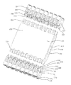
- FIG. 1 is a perspective view of a connector according to an embodiment
- FIG. 2 is an exploded view of the connector of FIG. 1 ;
- FIG. 3 is a cross-sectional view of the connector of FIG. 1 ;
- FIG. 4 is another perspective view of the connector of FIG. 1 (with the first case, the second case and the third case being removed);
- FIG. 5 is an exploded view of the connector of FIG. 4 ;
- FIG. 6 is an exploded view of a first connecting member of the connector of FIG. 1 :
- FIG. 7 is an exploded view of a third connecting member of the connector of FIG. 1 ;
- FIG. 8 is an exploded view of a second connecting member of the connector of FIG. 1 .
- a connector 10 is gusset plate connector with a floating tolerance insensitive.
- the connector 10 includes a first connecting member 100 , a second connecting member 200 and a third connecting member 300 .
- the first connecting member 100 includes a first case 110 , a first insulator 120 , and a first conductive terminal 130 , the first case 110 defines a first receiving chamber 112 therein, the first insulator 120 is received in the first receiving chamber 112 , and the first conductive terminal 130 is received in the first insulator 120 .
- An external sidewall of the first case 110 is provided with a first step 114 .
- the second connecting member 200 includes a second case 210 and a PCB board 220 , the second case 210 defines a containing hole 212 , the PCB board 222 is received in the containing hole 212 .
- a first end and a second end of the second case 210 each defines a latching groove 214 , the latching grooves 214 are in communication with the containing hole 212 .
- opposite ends of the PCB board 220 are provided with a first contact sheet 222 and a second contact sheet 224 .
- the first step 114 is received in the latching groove 214 of the first end.
- the first conductive terminal 130 resists the first contact sheet 222 , and the first conductive terminal 130 is capable of sliding along a first direction on the first contact sheet 222 .
- the third connecting member 300 includes a third case 310 , a second insulator 320 , and a second conductive terminal 330
- the third case 310 defines a second receiving chamber 312 therein
- the second insulator 320 is received in the second receiving chamber 312
- the second conductive terminal 330 is received in the second insulator 320
- An external sidewall of the third case 310 is provided with a second step 314
- the second step 314 is received in the latching groove 214 of the second end, also referring to FIG. 4
- the second conductive terminal 330 resists the second contact sheet 224
- the second conductive terminal 330 is capable of sliding along a second direction on the second contact sheet 224 .
- the third connecting member 300 is capable of sliding along a third direction on the second case 210 .
- an end of the first connecting member 100 is coupled to a first electrical component (not shown), the other end is coupled to the second connecting member 200 .
- An end of the third connecting member 300 is coupled to the second connecting member 200 , the other end is coupled to a second electrical component (not shown).
- the first connecting member 100 is a fixed connecting member
- the second connecting member 200 is an intermediate connecting member
- the third connecting member 300 is a slidable connecting member.
- Outer shapes of the first case 110 , the second case 210 and the third case 310 are cuboids. As shown in FIG.
- an external side of the first case 110 which is coupled to the second case 210 is provided with the first step 114 .
- An external side of the third case 310 which is coupled to the second case 210 is provided with the second step 314 .
- a first end and a second end of the second case 210 defines a latching groove 214 , the first step 114 is received in the latching groove 214 of the first end, the second step 314 is received in the latching groove 214 of the second end.
- the second case 210 defines a containing hole 212 for receiving the PCT board 220 .
- the containing hole 212 is in communication with the latching grooves 214 of the two ends respectively.
- the PCB board 220 is a relative thinner flat board.
- a surface of a first end of the PCB board 220 is provided with the first contact sheet 222
- a surface of a second end is provided with a second contact sheet 224 .
- a width of the first contact sheet 222 is greater than a width of the second contact sheet 224
- a length of the first contact sheet 222 is less than a length of the second contact sheet 224 .
- the first conductive terminal 130 and the second conductive terminal 330 both are signal terminals. The first conducive terminal 130 resists the first contact sheet 222
- the second conducive terminal 330 resists the second contact sheet 224 .
- a surface of the PCB board 220 is a flat surface, a direction oriented from a first edge of the PCB board 220 to a second edge is defined as the second direction, i.e. the Z axis direction.
- a direction parallel to the first edge of the PCB board 220 is defined as the first direction, i.e. the X axis direction.
- a direction perpendicular to the surface of the PCB board 220 is defined as the third direction, i.e. the Y axis direction.
- the first contact sheet 222 extends along a direction parallel to the X axis direction
- the second contact sheet 224 extends along a direction parallel to the Z axis direction.
- the first conductive terminal 130 is capable of sliding along a direction parallel to the X axis direction, to enable the second connecting member 200 to sliding along the X axis direction relative to the first connecting member 100 .
- the second conductive terminal 330 is capable of sliding along a direction parallel to the Z axis direction, to enable the third connecting member 300 to sliding along the Z axis direction relative to the second connecting member 200 .
- the third connecting member 300 is capable of sliding along the third direction on the second case 210 , i.e. the third connecting member 300 is capable of sling along the Y axis direction relative to the first connecting member 100 .
- the first direction, the second direction, and the third direction are perpendicular to each other.
- the first step 114 is received in the latching groove 214 of the first end, and the first conductive terminal 130 resists the first contact sheet 222 .
- the first connecting member 100 slides along the first direction relative to the second connecting member 200 .
- the second step 314 is received in the latching groove 214 of the second end, and the second conductive terminal 330 resists the second contact sheet 224 .
- the third connecting member 100 slides along the second direction relative to the second connecting member 200 .
- the third connecting member 300 can slide along the third direction on the second case 210 .
- the electrical components coupled to opposite ends of the connector 10 can slide along three directions which are perpendicular to each other, i.e. deviations in the design of the structure of the electrical components on opposite ends of the connector 10 are allowed, such that a problem of a difficulty of a connection between the connector 10 and the electrical components which is caused by a deviation of the design of the structure of the electrical components can be avoided, thereby a tolerance insensitive of the connector 10 is enhanced.
- the connector 10 further includes a third conductive terminal 400 , a fourth conductive terminal 500 , and a third contact sheet 600 .
- the first insulator 120 includes a first portion 122 and a second portion 124 , the first portion 122 is plugged to the second portion 124 , the first conductive terminal 130 is received in the first portion 122 , the third conductive terminal 400 is received in the second portion 124 .
- the second insulator 320 includes a third portion 322 and a fourth portion 324 , the third portion 322 is plugged to the fourth portion 324 .
- the second conductive terminal 330 is received the third portion 322
- the third conductive terminal 500 is received in the fourth portion 324 .
- the third contact sheet 600 is positioned on the PCB board 220
- the first contact sheet 222 , the second contact sheet 224 , and the third contact sheet 600 are all positioned on a same side surface of the PCB board 220 .
- separation distances are provided between the first contact sheet 222 and the third contact sheet 600 , between the second contact sheet 224 and the third contact sheet 600 .
- the third conductive terminal 400 and the fourth conductive terminal 500 both resist the third contact sheet 600 .
- FIG. 1 shows the embodiment, as shown in FIG.
- the first conductive terminal 130 and the first portion 122 are integrally formed
- the third conductive terminal 400 and the second portion 124 are integrally formed.
- the second conductive terminal 330 and the third portion 322 are integrally formed
- the fourth conductive terminal 500 and the fourth portion 324 are integrally formed.
- a number of the third contact sheet 600 is two, the two third contact sheets 600 are positioned on opposite sides of the PCB board 220 respectively.
- the third conductive terminal 400 includes two first terminal units 410 positioned on the second portion 124 and opposite to each other. The two first terminal units 410 clamp the PCB board 220 , and the two first terminal units 410 resist the two third contact sheets 600 correspondingly.
- the fourth conductive terminal 500 includes two second terminal units 510 positioned on the fourth portion 324 and opposite to each other. The two second terminal units 510 clamp the PCB board 220 , and the two second terminal units 510 resist the two third contact sheets 600 correspondingly.
- the two first terminal units 410 and the two second terminal units 510 both clamp the PCB board 220 .
- the third connecting member 300 slides along a direction parallel to a thickness direction of the second case 210 , the third conductive terminal 400 and the fourth conductive terminal 500 can maintain a reliable contact with the third contact sheet 600 on the PCB board 200 , thereby ensuring a closed transmission of the signal.
- the third conductive terminal 400 and the fourth conductive terminal 500 both are ground terminals, as shown in FIG. 6
- the third conductive terminal 400 includes two first terminal units 410 .
- the fourth conductive terminal 500 includes two second terminal units 510 .
- Each first terminal unit 410 and each second terminal unit 510 includes a fixing portion and a resisting portion.
- the second portion 124 has a cuboids shape, and the second portion 124 defines a gate groove for receiving the first portion 122 .
- the two first terminal units 410 are positioned on the top and the bottom of the second portion 124 .
- the fixing portion of the two first terminal units 410 and the second portion 124 are integrally formed.
- the resisting portions of the two first terminal units 410 each has a bent shape, and the resisting portions of the two first terminal units 410 resist opposite sides of the PCB board 220 , to enable the two first terminal units 410 to clamp the PCB board 220 , and the two first terminal units 410 resist the third contact sheets 600 on opposite sides of the PCB board 220 .
- the fourth portion 324 has a cuboids shape, and the fourth portion 324 defines a gate groove for receiving the third portion 322 .
- the two second terminal units 510 are positioned on the top and the bottom of the fourth portion 324 .
- the fixing portion of the two second terminal units 510 and the fourth portion 324 are integrally formed.
- the resisting portions of the two second terminal units 510 each has a bent shape, and the resisting portions of the two second terminal units 510 resist opposite sides of the PCB board 220 , to enable the two second terminal units 510 to clamp the PCB board 220 , and the two second terminal units 510 resist the third contact sheets 600 on opposite sides of the PCB board 220 , and cause the third conductive terminal 400 and the fourth conductive terminal 500 to reliability contact the third contact sheet 600 .
- a first side surface of the PCB board 220 is provided with a first contact sheet 222 , a second contact sheet 224 and one third contact sheet 600 , a second side surface is provided with another one third contact sheet 600 .
- a surface of the third contact sheet 600 defines a plurality of vias 610 .
- a number of the first portion 122 , the first conductive terminal 130 , the third conductive terminal 400 , and the second portion 124 each is more than two
- the plurality of first conductive terminals 130 is received in the plurality of first portions 122 correspondingly.
- the plurality of first portions 122 are plugged to the plurality of second portions 124 correspondingly.
- the plurality of third conductive terminals 400 is received the plurality of second portions 124 correspondingly.
- the plurality of second portions 124 are received in the first receiving groove 112 side by side.
- a number of the first contact sheets 222 is more than two, the plurality of first contact sheets 222 is arranged along a first direction and spaced from each other, the plurality of first conductive terminals 130 resists the plurality of first contact sheets 222 correspondingly.
- the plurality of third conductive terminals 400 and the plurality of first conductive terminals 130 are alternatively arranged, the plurality of third conductive terminals 400 resists the third contact sheet 600 .
- a number of the third portions 322 , the second conductive terminals 330 , the fourth conductive terminals 500 , and the fourth portions 324 each is more than two.
- the plurality of second conductive terminals 330 is received in the plurality of third portions 322 , the plurality of third portions 322 is plugged to the plurality of fourth portions 324 , the plurality of fourth conductive terminals 500 is received in the plurality of fourth portions 324 correspondingly.
- the plurality of fourth portions 324 is received in the second receiving chamber 312 side by side.
- a number of the second conductive sheets 224 is more than two, the plurality of second conductive sheets 224 is arranged along the first direction and spaced from each other.
- the plurality of second conductive terminals 330 resists the plurality of second contact sheets 224 correspondingly.
- the plurality of fourth conductive terminals 500 and the plurality of second conductive terminals 330 are alternatively arranged, the plurality of fourth conductive terminals 500 resists the third contact sheet 600 , enabling the connector 10 to transmit signals by multiple passages, and the transmission efficient of the connector 10 is enhanced.
- the first case 110 defines a first receiving chamber 112 along a direction parallel to an axial direction of the second case 210 .
- a number of the first portion 122 and the second portion 124 each is more than two, the plurality of second portions 124 are arranged in two rows in the first receiving chamber 112 .
- the plurality of first portions 122 are plugged to the plurality of second portions 124 correspondingly.
- the plurality of first conductive terminals 130 is received in the plurality of first portions 122 correspondingly.
- the plurality of third conductive terminals 400 is received in the plurality of second portions 124 correspondingly.
- the plurality of first conductive terminals 130 resists the plurality of first contact sheets 222 correspondingly.
- the plurality of third conductive terminals 400 resists the third contact sheet 600 .
- the plurality of second portions 124 can also be aligned in a row or several rows in the first receiving groove 112 .
- the third case 310 defines a second receiving chamber 312 along a direction parallel to an axial direction of the second case 210 .
- a number of the second portion 322 and the fourth portion 324 each is more than two, the plurality of fourth portions 324 are arranged in two rows in the second receiving chamber 312 .
- the plurality of third portions 322 are plugged to the plurality of fourth portions 324 correspondingly.
- the plurality of second conductive terminals 330 is received in the plurality of third portions 322 correspondingly.
- the plurality of fourth conductive terminals 500 is received in the plurality of fourth portions 324 correspondingly.
- the plurality of second conductive terminals 330 resists the plurality of second contact sheets 224 correspondingly.
- the plurality of fourth conductive terminals 500 resists the third contact sheet 600 .
- the plurality of third portions 322 can also be aligned in a row or a plurality of rows in the second receiving groove 312 .
- a number of the first receiving grooves 112 , the second receiving grooves 312 , the containing hole 212 and the PCB board 220 each is two, the two first receiving groove 112 are defined on the first case 110 side by side, the two second receiving groove 312 are defined on the second case 210 side by side.
- opposite ends of the two containing holes 222 are in communication with the latching groove 214 .
- the two PCB boards 220 are received in the two containing holes 212 correspondingly, and the two PCB boards 220 are positioned opposite to each other. It can be understood that, in other embodiments, a number of the first receiving groove 112 , the second receiving groove 212 , the containing hole 212 and the PCB board 220 each can be one or more than two.
- the connector 10 further includes a first conductive sheet 700 and a second conductive sheet 800 .
- the first conductive sheet 700 is positioned on the second portion 124 , and the plurality of third conductive terminals 400 are electrically coupled to the first conductive sheet 700 .
- the second conductive sheet 800 is positioned on the fourth portion 324 , and the plurality of fourth conductive terminals 500 are electrically coupled to the second conductive sheet 800 .
- FIG. 6 the first conductive sheet 700 is positioned on the second portion 124 , and the plurality of third conductive terminals 400 are electrically coupled to the first conductive sheet 700 .
- the second conductive sheet 800 is positioned on the fourth portion 324 , and the plurality of fourth conductive terminals 500 are electrically coupled to the second conductive sheet 800 .
- the connector 10 further includes a first shielding sheet 900 and a second shielding sheet 1100 . As shown in FIG.
- the first portion 122 defines a first groove 1222
- the second portion 124 defines a second groove 1242
- the first shielding sheet 900 is received in the first groove 1222 and the second groove 1242 respectively.
- the third portion 322 defines a third groove 3222
- the fourth portion 324 defines a fourth groove 3242
- the second shielding sheet 1100 is received in the third groove 3222 and the fourth groove 3242 respectively, such that a reliable signal transmission can be ensured.
- a slidable displacement of the first conductive terminal 130 along the first direction on the first contact sheet 222 is denoted as S, 0.5 millimeters ⁇ S ⁇ 1 millimeters.
- the slidable distance of the first conductive terminal 130 along the first direction on the first contact sheet 222 is equal to a slidable distance of the first conductive terminal 130 along a direction parallel to the X axis direction, i.e. the slidable displacement of the second connecting member 200 along the X axis direction relative to the first connecting member 100 .
- the slidable displacement of the second connecting member 200 along the X axis direction relative to the first connecting member 100 is 0.7 millimeters, i.e.
- values of a slidable displacement of the second connecting member 200 relative to a left side and a right side of the first connecting member 100 both are 0.7 millimeters. It can be understood, the electrical components connected to opposite ends of the connector 10 allow a position deviation value of 0.7 millimeters along the X axis direction.
- a cross section of the containing hole 212 has a shape which shrinks from opposite ends toward a middle portion, and can allow a deflection of opposite ends of the PCB board in a range.
- a slidable distance of the third connecting member 300 along the third direction on the second case 210 is denoted as d, 0.5 millimeters ⁇ d ⁇ 1 millimeters.
- a slidable distance of the third connecting member 300 along the Y axis direction relative to the second connecting member 200 is equal to the slidable distance of the third connecting member 300 along the third direction on the second case 210 .
- a slidable displacement of the third connecting member 300 along the Y axis direction relative to the second connecting member 200 is 0.7 millimeters, i.e. values of slidable displacements of the third connecting member 300 relative to an upper side and a lower side of the second connecting member 200 both are 0.7 millimeters.
- the electrical components connected to opposite ends of the connector 10 allow a position deviation value of 0.7 millimeters along the Y axis direction.
- a slidable displacement of the second conductive terminal 330 along the second direction on the second contact sheet 224 is denoted as L, 1.0 millimeters ⁇ L ⁇ 3 millimeters.
- a slidable displacement of the second conductive terminal 330 along a direction parallel to the Z axis direction is equal to the slidable displacement of the second conductive terminal 330 along the second direction on the second contact sheet 224 , i.e. a sidable displacement of the third connecting member 300 along the Z axis direction relative to the second connecting member 200 .
- a sidable displacement of the third connecting member 300 along the Z axis direction relative to the second connecting member 200 is 2.0 millimeters, i.e.
- the value of the slidable displacement of the third connecting member 300 towards or away from the second connecting member 200 is 2.0 millimeters. It can be understood, the electrical components connected to opposite ends of the connector 10 allow a position deviation value of 2.0 millimeters along the Z axis direction
Applications Claiming Priority (4)
| Application Number | Priority Date | Filing Date | Title |
|---|---|---|---|
| CN201610368104 | 2016-05-27 | ||
| CN201610368104.7 | 2016-05-27 | ||
| CN201610368104.7A CN105896145B (zh) | 2016-05-27 | 2016-05-27 | 连接器 |
| PCT/CN2016/089816 WO2017201834A1 (zh) | 2016-05-27 | 2016-07-12 | 连接器 |
Publications (2)
| Publication Number | Publication Date |
|---|---|
| US20170373413A1 US20170373413A1 (en) | 2017-12-28 |
| US10044120B2 true US10044120B2 (en) | 2018-08-07 |
Family
ID=56710634
Family Applications (1)
| Application Number | Title | Priority Date | Filing Date |
|---|---|---|---|
| US15/116,483 Active 2036-08-25 US10044120B2 (en) | 2016-05-27 | 2016-07-12 | Connector |
Country Status (7)
| Country | Link |
|---|---|
| US (1) | US10044120B2 (de) |
| EP (1) | EP3467950B1 (de) |
| JP (1) | JP6498681B2 (de) |
| KR (1) | KR101878049B1 (de) |
| CN (1) | CN105896145B (de) |
| TW (1) | TWI621311B (de) |
| WO (1) | WO2017201834A1 (de) |
Cited By (4)
| Publication number | Priority date | Publication date | Assignee | Title |
|---|---|---|---|---|
| US20180301837A1 (en) * | 2017-04-14 | 2018-10-18 | Amphenol Corporation | Float connector for interconnecting printed circuit boards |
| US10446955B2 (en) | 2017-04-14 | 2019-10-15 | Amphenol Corporation | Shielded connector for interconnecting printed circuit boards |
| US10505302B2 (en) * | 2017-11-28 | 2019-12-10 | Tyco Electronics Japan G.K. | Connector |
| US11056807B2 (en) | 2017-04-14 | 2021-07-06 | Amphenol Corporation | Float connector for interconnecting printed circuit boards |
Families Citing this family (3)
| Publication number | Priority date | Publication date | Assignee | Title |
|---|---|---|---|---|
| CN106898885B (zh) * | 2017-01-03 | 2019-03-19 | 新华三技术有限公司 | 分线器和分线系统 |
| CN109599689B (zh) | 2017-09-30 | 2020-11-17 | 中航光电科技股份有限公司 | 连接器组件 |
| CN111224253A (zh) | 2018-11-23 | 2020-06-02 | 深圳市深台帏翔电子有限公司 | 连接器 |
Citations (15)
| Publication number | Priority date | Publication date | Assignee | Title |
|---|---|---|---|---|
| US6293826B1 (en) | 2000-12-28 | 2001-09-25 | Hon Hai Precision Ind. Co., Ltd. | Electrical connector with metal side members and method of producing same |
| CN2507156Y (zh) | 2001-09-10 | 2002-08-21 | 莫列斯公司 | 电连接器 |
| US6623310B1 (en) * | 2002-05-21 | 2003-09-23 | Hon Hai Precision Ind. Co., Ltd. | High density electrical connector assembly with reduced insertion force |
| US6695622B2 (en) * | 2002-05-31 | 2004-02-24 | Hon Hai Precision Ind. Co., Ltd. | Electrical system having means for accommodating various distances between PC boards thereof mounting the means |
| US7481679B1 (en) * | 2006-11-01 | 2009-01-27 | Emc Corporation | Electrical connector and circuit card assembly |
| US7494383B2 (en) * | 2007-07-23 | 2009-02-24 | Amphenol Corporation | Adapter for interconnecting electrical assemblies |
| US7637784B2 (en) * | 2007-01-29 | 2009-12-29 | Fci Americas Technology, Inc. | Disk drive interposer |
| CN102683929A (zh) | 2012-06-06 | 2012-09-19 | 上海雷迪埃电子有限公司 | 射频连接器 |
| CN202444086U (zh) | 2012-03-08 | 2012-09-19 | 深圳立讯精密工业股份有限公司 | 连接器 |
| US8740643B2 (en) * | 2011-08-02 | 2014-06-03 | Hon Hai Precision Industry Co., Ltd. | Electrical receptacle connector compatible with existing electrical plug and complementary plug |
| CN204696287U (zh) | 2015-05-29 | 2015-10-07 | 深圳市深台帏翔电子有限公司 | 电连接器 |
| US20160006191A1 (en) * | 2014-07-01 | 2016-01-07 | Tyco Electronics Corporation | Electrical connector having electrical contacts configured to reduce wear caused by wiping |
| CN205029062U (zh) | 2015-09-29 | 2016-02-10 | 凡甲电子(苏州)有限公司 | 电连接器 |
| US9306336B2 (en) * | 2014-04-25 | 2016-04-05 | Speed Tech Corp. | High frequency connector |
| CN205790554U (zh) | 2016-05-27 | 2016-12-07 | 深圳市深台帏翔电子有限公司 | 连接器 |
Family Cites Families (14)
| Publication number | Priority date | Publication date | Assignee | Title |
|---|---|---|---|---|
| JPH0344882U (de) * | 1989-09-07 | 1991-04-25 | ||
| JPH04253174A (ja) * | 1991-01-29 | 1992-09-08 | Fujitsu Ltd | コネクタの接続機構とそれを用いたコネクタ |
| JP2001307831A (ja) | 2000-04-19 | 2001-11-02 | Jst Mfg Co Ltd | プリント配線板用コネクタ |
| JP2004265599A (ja) * | 2002-12-19 | 2004-09-24 | Iriso Denshi Kogyo Kk | 基板接続用コネクタ及びコネクタ接続用基板 |
| US7044748B2 (en) * | 2003-09-26 | 2006-05-16 | Hon Hai Precision Ind. Co., Ltd | Electrical device for interconnecting two printed circuit boards at a large distance |
| JP4295270B2 (ja) * | 2005-11-16 | 2009-07-15 | 日本航空電子工業株式会社 | コネクタ及び相手方コネクタ並びにそれらの組立体 |
| SG145604A1 (en) * | 2007-03-08 | 2008-09-29 | 3M Innovative Properties Co | Connector apparatus |
| JP4514065B2 (ja) * | 2007-09-10 | 2010-07-28 | ヒロセ電機株式会社 | 基板用電気コネクタ及びこれと中間電気コネクタとを有する電気コネクタ組立体 |
| DE102009015462B4 (de) * | 2008-11-10 | 2014-10-30 | Erni Production Gmbh & Co. Kg | Winkel-Steckverbinder mit einer Abschirmung und Verfahren zur Herstellung der Abschirmung des Winkel-Steckverbinders |
| CN102201624B (zh) * | 2010-03-26 | 2014-02-26 | 3M创新有限公司 | 电连接器和电连接器组件 |
| JP5840649B2 (ja) * | 2013-05-29 | 2016-01-06 | ヒロセ電機株式会社 | 電気コネクタ、該電気コネクタと相手コネクタとを有する電気コネクタ組立体 |
| JP6190202B2 (ja) * | 2013-08-06 | 2017-08-30 | ヒロセ電機株式会社 | 電気コネクタ |
| CN203445286U (zh) * | 2013-09-16 | 2014-02-19 | 罗森伯格亚太电子有限公司 | 板对板射频连接器及其适配器 |
| JP5860917B2 (ja) * | 2014-04-08 | 2016-02-16 | 日本航空電子工業株式会社 | プリント配線板 |
-
2016
- 2016-05-27 CN CN201610368104.7A patent/CN105896145B/zh active Active
- 2016-07-12 WO PCT/CN2016/089816 patent/WO2017201834A1/zh active Application Filing
- 2016-07-12 EP EP16741840.9A patent/EP3467950B1/de active Active
- 2016-07-12 JP JP2016549547A patent/JP6498681B2/ja not_active Expired - Fee Related
- 2016-07-12 US US15/116,483 patent/US10044120B2/en active Active
- 2016-08-02 KR KR1020160098386A patent/KR101878049B1/ko active IP Right Grant
- 2016-08-03 TW TW105124653A patent/TWI621311B/zh active
Patent Citations (15)
| Publication number | Priority date | Publication date | Assignee | Title |
|---|---|---|---|---|
| US6293826B1 (en) | 2000-12-28 | 2001-09-25 | Hon Hai Precision Ind. Co., Ltd. | Electrical connector with metal side members and method of producing same |
| CN2507156Y (zh) | 2001-09-10 | 2002-08-21 | 莫列斯公司 | 电连接器 |
| US6623310B1 (en) * | 2002-05-21 | 2003-09-23 | Hon Hai Precision Ind. Co., Ltd. | High density electrical connector assembly with reduced insertion force |
| US6695622B2 (en) * | 2002-05-31 | 2004-02-24 | Hon Hai Precision Ind. Co., Ltd. | Electrical system having means for accommodating various distances between PC boards thereof mounting the means |
| US7481679B1 (en) * | 2006-11-01 | 2009-01-27 | Emc Corporation | Electrical connector and circuit card assembly |
| US7637784B2 (en) * | 2007-01-29 | 2009-12-29 | Fci Americas Technology, Inc. | Disk drive interposer |
| US7494383B2 (en) * | 2007-07-23 | 2009-02-24 | Amphenol Corporation | Adapter for interconnecting electrical assemblies |
| US8740643B2 (en) * | 2011-08-02 | 2014-06-03 | Hon Hai Precision Industry Co., Ltd. | Electrical receptacle connector compatible with existing electrical plug and complementary plug |
| CN202444086U (zh) | 2012-03-08 | 2012-09-19 | 深圳立讯精密工业股份有限公司 | 连接器 |
| CN102683929A (zh) | 2012-06-06 | 2012-09-19 | 上海雷迪埃电子有限公司 | 射频连接器 |
| US9306336B2 (en) * | 2014-04-25 | 2016-04-05 | Speed Tech Corp. | High frequency connector |
| US20160006191A1 (en) * | 2014-07-01 | 2016-01-07 | Tyco Electronics Corporation | Electrical connector having electrical contacts configured to reduce wear caused by wiping |
| CN204696287U (zh) | 2015-05-29 | 2015-10-07 | 深圳市深台帏翔电子有限公司 | 电连接器 |
| CN205029062U (zh) | 2015-09-29 | 2016-02-10 | 凡甲电子(苏州)有限公司 | 电连接器 |
| CN205790554U (zh) | 2016-05-27 | 2016-12-07 | 深圳市深台帏翔电子有限公司 | 连接器 |
Non-Patent Citations (3)
| Title |
|---|
| ISR of PCT/CN2016/089816 dated Jan. 25, 2017. |
| SIPO Office Action of corresponding Chinese patent application dated Jul. 12, 2017. |
| Taiwanese Office Action of corresponding patent application in Taiwan dated Aug. 15, 2017. |
Cited By (7)
| Publication number | Priority date | Publication date | Assignee | Title |
|---|---|---|---|---|
| US20180301837A1 (en) * | 2017-04-14 | 2018-10-18 | Amphenol Corporation | Float connector for interconnecting printed circuit boards |
| US10446955B2 (en) | 2017-04-14 | 2019-10-15 | Amphenol Corporation | Shielded connector for interconnecting printed circuit boards |
| US10505303B2 (en) * | 2017-04-14 | 2019-12-10 | Amphenol Corporation | Float connector for interconnecting printed circuit boards |
| US10665976B2 (en) | 2017-04-14 | 2020-05-26 | Amphenol Corporation | Float connector for interconnecting printed circuit boards |
| US11056807B2 (en) | 2017-04-14 | 2021-07-06 | Amphenol Corporation | Float connector for interconnecting printed circuit boards |
| US11901654B2 (en) | 2017-04-14 | 2024-02-13 | Amphenol Corporation | Method of interconnecting printed circuit boards |
| US10505302B2 (en) * | 2017-11-28 | 2019-12-10 | Tyco Electronics Japan G.K. | Connector |
Also Published As
| Publication number | Publication date |
|---|---|
| TW201742331A (zh) | 2017-12-01 |
| CN105896145A (zh) | 2016-08-24 |
| CN105896145B (zh) | 2018-05-08 |
| JP6498681B2 (ja) | 2019-04-10 |
| JP2018518791A (ja) | 2018-07-12 |
| EP3467950A4 (de) | 2020-01-01 |
| TWI621311B (zh) | 2018-04-11 |
| KR101878049B1 (ko) | 2018-08-09 |
| WO2017201834A1 (zh) | 2017-11-30 |
| US20170373413A1 (en) | 2017-12-28 |
| KR20170134150A (ko) | 2017-12-06 |
| EP3467950A1 (de) | 2019-04-10 |
| EP3467950B1 (de) | 2021-11-17 |
Similar Documents
| Publication | Publication Date | Title |
|---|---|---|
| US10044120B2 (en) | Connector | |
| US7980893B2 (en) | Coaxial connector and connector device | |
| US7708603B1 (en) | Electrical connector with improved crosstalk features | |
| US20140073173A1 (en) | Electrical connector | |
| US9362695B2 (en) | Electrical connector | |
| KR20120089745A (ko) | 플러그 어댑터 | |
| US9166350B2 (en) | Hybrid electrical connector | |
| KR20160080636A (ko) | 전기 커넥터의 컨택트 및 이를 포함하는 전기 커넥터 | |
| US8814585B2 (en) | Electrical connector having a positioning protrusion with a slanted guiding surface | |
| US20170133779A1 (en) | Electrical Connector | |
| KR102430924B1 (ko) | 커넥터 및 커넥터 조립체 | |
| US11355876B2 (en) | Electrical connector for printed circuit boards | |
| US9614334B2 (en) | Hermaphroditic electrical connector | |
| US9774146B2 (en) | Cable connector assembly with improved printed circuit board module | |
| KR101488891B1 (ko) | 기판 대 기판 커넥터 어셈블리 | |
| US8052460B1 (en) | Electrical connector assembly and adjustable receiving connector thereof | |
| US9431736B2 (en) | Card edge connector and card edge connector assembly | |
| US8523613B2 (en) | Electrical connector for broadside coupled or edge coupled mating with mating connector | |
| US8007322B2 (en) | Connector component and connector device | |
| KR200496943Y1 (ko) | 버클 커넥터 | |
| KR200492776Y1 (ko) | 커넥터 | |
| US8506309B2 (en) | Electrical connector with improved signal transmitting performance | |
| US20130095684A1 (en) | Electrical connector | |
| US20160172800A1 (en) | Universal serial bus jack, universal serial bus plug and universal serial bus connector assembly | |
| US20220329012A1 (en) | Connector assembly |
Legal Events
| Date | Code | Title | Description |
|---|---|---|---|
| AS | Assignment |
Owner name: SHENZHEN SHENTAI WEIXIANG ELECTRONICS CO., LTD., C Free format text: ASSIGNMENT OF ASSIGNORS INTEREST;ASSIGNORS:WANG, JIAN;CHEN, PING;REEL/FRAME:039335/0605 Effective date: 20160728 |
|
| FEPP | Fee payment procedure |
Free format text: ENTITY STATUS SET TO SMALL (ORIGINAL EVENT CODE: SMAL); ENTITY STATUS OF PATENT OWNER: SMALL ENTITY |
|
| STCF | Information on status: patent grant |
Free format text: PATENTED CASE |
|
| FEPP | Fee payment procedure |
Free format text: PETITION RELATED TO MAINTENANCE FEES GRANTED (ORIGINAL EVENT CODE: PTGR); ENTITY STATUS OF PATENT OWNER: SMALL ENTITY |
|
| MAFP | Maintenance fee payment |
Free format text: PAYMENT OF MAINTENANCE FEE, 4TH YR, SMALL ENTITY (ORIGINAL EVENT CODE: M2551); ENTITY STATUS OF PATENT OWNER: SMALL ENTITY Year of fee payment: 4 |