TWI790984B - Light-emitting device - Google Patents
Light-emitting device Download PDFInfo
- Publication number
- TWI790984B TWI790984B TW111131100A TW111131100A TWI790984B TW I790984 B TWI790984 B TW I790984B TW 111131100 A TW111131100 A TW 111131100A TW 111131100 A TW111131100 A TW 111131100A TW I790984 B TWI790984 B TW I790984B
- Authority
- TW
- Taiwan
- Prior art keywords
- semiconductor layer
- light
- layer
- semiconductor
- emitting element
- Prior art date
Links
- 239000004065 semiconductor Substances 0.000 claims abstract description 180
- 239000010410 layer Substances 0.000 description 253
- 239000000758 substrate Substances 0.000 description 32
- 239000000463 material Substances 0.000 description 24
- 230000004888 barrier function Effects 0.000 description 23
- BASFCYQUMIYNBI-UHFFFAOYSA-N platinum Chemical compound [Pt] BASFCYQUMIYNBI-UHFFFAOYSA-N 0.000 description 23
- 238000012360 testing method Methods 0.000 description 22
- 239000010936 titanium Substances 0.000 description 18
- PXHVJJICTQNCMI-UHFFFAOYSA-N Nickel Chemical compound [Ni] PXHVJJICTQNCMI-UHFFFAOYSA-N 0.000 description 15
- 239000011651 chromium Substances 0.000 description 14
- 238000009826 distribution Methods 0.000 description 13
- 238000000034 method Methods 0.000 description 11
- 229910052697 platinum Inorganic materials 0.000 description 10
- 229910052719 titanium Inorganic materials 0.000 description 10
- 238000005240 physical vapour deposition Methods 0.000 description 9
- 230000008569 process Effects 0.000 description 9
- 229910052782 aluminium Inorganic materials 0.000 description 8
- 239000010931 gold Substances 0.000 description 8
- 238000009413 insulation Methods 0.000 description 8
- 239000002356 single layer Substances 0.000 description 8
- 229910052721 tungsten Inorganic materials 0.000 description 8
- VYPSYNLAJGMNEJ-UHFFFAOYSA-N Silicium dioxide Chemical compound O=[Si]=O VYPSYNLAJGMNEJ-UHFFFAOYSA-N 0.000 description 7
- RTAQQCXQSZGOHL-UHFFFAOYSA-N Titanium Chemical compound [Ti] RTAQQCXQSZGOHL-UHFFFAOYSA-N 0.000 description 7
- XAGFODPZIPBFFR-UHFFFAOYSA-N aluminium Chemical compound [Al] XAGFODPZIPBFFR-UHFFFAOYSA-N 0.000 description 7
- 229910052804 chromium Inorganic materials 0.000 description 7
- OGIDPMRJRNCKJF-UHFFFAOYSA-N titanium oxide Inorganic materials [Ti]=O OGIDPMRJRNCKJF-UHFFFAOYSA-N 0.000 description 7
- 239000004925 Acrylic resin Substances 0.000 description 6
- 229920000178 Acrylic resin Polymers 0.000 description 6
- 229920000089 Cyclic olefin copolymer Polymers 0.000 description 6
- KDLHZDBZIXYQEI-UHFFFAOYSA-N Palladium Chemical compound [Pd] KDLHZDBZIXYQEI-UHFFFAOYSA-N 0.000 description 6
- 239000004697 Polyetherimide Substances 0.000 description 6
- 239000004642 Polyimide Substances 0.000 description 6
- UMIVXZPTRXBADB-UHFFFAOYSA-N benzocyclobutene Chemical compound C1=CC=C2CCC2=C1 UMIVXZPTRXBADB-UHFFFAOYSA-N 0.000 description 6
- 239000010949 copper Substances 0.000 description 6
- 238000010586 diagram Methods 0.000 description 6
- 239000003989 dielectric material Substances 0.000 description 6
- 238000005530 etching Methods 0.000 description 6
- 229920002313 fluoropolymer Polymers 0.000 description 6
- 229910010272 inorganic material Inorganic materials 0.000 description 6
- 239000011147 inorganic material Substances 0.000 description 6
- 239000012811 non-conductive material Substances 0.000 description 6
- BCCOBQSFUDVTJQ-UHFFFAOYSA-N octafluorocyclobutane Chemical compound FC1(F)C(F)(F)C(F)(F)C1(F)F BCCOBQSFUDVTJQ-UHFFFAOYSA-N 0.000 description 6
- 235000019407 octafluorocyclobutane Nutrition 0.000 description 6
- 239000011368 organic material Substances 0.000 description 6
- 229920003229 poly(methyl methacrylate) Polymers 0.000 description 6
- 229920001601 polyetherimide Polymers 0.000 description 6
- 229920000139 polyethylene terephthalate Polymers 0.000 description 6
- 239000005020 polyethylene terephthalate Substances 0.000 description 6
- 229920001721 polyimide Polymers 0.000 description 6
- 239000004926 polymethyl methacrylate Substances 0.000 description 6
- 238000004544 sputter deposition Methods 0.000 description 6
- VYZAMTAEIAYCRO-UHFFFAOYSA-N Chromium Chemical compound [Cr] VYZAMTAEIAYCRO-UHFFFAOYSA-N 0.000 description 5
- 239000011521 glass Substances 0.000 description 5
- 229910052759 nickel Inorganic materials 0.000 description 5
- 238000000206 photolithography Methods 0.000 description 5
- 238000002310 reflectometry Methods 0.000 description 5
- 229910052814 silicon oxide Inorganic materials 0.000 description 5
- WFKWXMTUELFFGS-UHFFFAOYSA-N tungsten Chemical compound [W] WFKWXMTUELFFGS-UHFFFAOYSA-N 0.000 description 5
- 239000010937 tungsten Substances 0.000 description 5
- 239000011701 zinc Substances 0.000 description 5
- PIGFYZPCRLYGLF-UHFFFAOYSA-N Aluminum nitride Chemical class [Al]#N PIGFYZPCRLYGLF-UHFFFAOYSA-N 0.000 description 4
- JMASRVWKEDWRBT-UHFFFAOYSA-N Gallium nitride Chemical compound [Ga]#N JMASRVWKEDWRBT-UHFFFAOYSA-N 0.000 description 4
- 229910045601 alloy Inorganic materials 0.000 description 4
- 239000000956 alloy Substances 0.000 description 4
- 238000000605 extraction Methods 0.000 description 4
- PCHJSUWPFVWCPO-UHFFFAOYSA-N gold Chemical compound [Au] PCHJSUWPFVWCPO-UHFFFAOYSA-N 0.000 description 4
- 229910052737 gold Inorganic materials 0.000 description 4
- 229910052751 metal Inorganic materials 0.000 description 4
- 239000007769 metal material Substances 0.000 description 4
- TWNQGVIAIRXVLR-UHFFFAOYSA-N oxo(oxoalumanyloxy)alumane Chemical compound O=[Al]O[Al]=O TWNQGVIAIRXVLR-UHFFFAOYSA-N 0.000 description 4
- 239000010948 rhodium Substances 0.000 description 4
- LIVNPJMFVYWSIS-UHFFFAOYSA-N silicon monoxide Chemical compound [Si-]#[O+] LIVNPJMFVYWSIS-UHFFFAOYSA-N 0.000 description 4
- 235000012431 wafers Nutrition 0.000 description 4
- 229910018072 Al 2 O 3 Inorganic materials 0.000 description 3
- RYGMFSIKBFXOCR-UHFFFAOYSA-N Copper Chemical compound [Cu] RYGMFSIKBFXOCR-UHFFFAOYSA-N 0.000 description 3
- 239000004593 Epoxy Substances 0.000 description 3
- 229910002601 GaN Inorganic materials 0.000 description 3
- 229910052581 Si3N4 Inorganic materials 0.000 description 3
- BQCADISMDOOEFD-UHFFFAOYSA-N Silver Chemical compound [Ag] BQCADISMDOOEFD-UHFFFAOYSA-N 0.000 description 3
- GWEVSGVZZGPLCZ-UHFFFAOYSA-N Titan oxide Chemical compound O=[Ti]=O GWEVSGVZZGPLCZ-UHFFFAOYSA-N 0.000 description 3
- 238000005229 chemical vapour deposition Methods 0.000 description 3
- 229910052802 copper Inorganic materials 0.000 description 3
- 239000003822 epoxy resin Substances 0.000 description 3
- 150000002148 esters Chemical class 0.000 description 3
- 238000001704 evaporation Methods 0.000 description 3
- ORUIBWPALBXDOA-UHFFFAOYSA-L magnesium fluoride Chemical compound [F-].[F-].[Mg+2] ORUIBWPALBXDOA-UHFFFAOYSA-L 0.000 description 3
- 229910001635 magnesium fluoride Inorganic materials 0.000 description 3
- 238000001451 molecular beam epitaxy Methods 0.000 description 3
- 239000004417 polycarbonate Substances 0.000 description 3
- 229920000515 polycarbonate Polymers 0.000 description 3
- 229920000647 polyepoxide Polymers 0.000 description 3
- -1 polyethylene terephthalate Polymers 0.000 description 3
- 229920001296 polysiloxane Polymers 0.000 description 3
- HQVNEWCFYHHQES-UHFFFAOYSA-N silicon nitride Chemical compound N12[Si]34N5[Si]62N3[Si]51N64 HQVNEWCFYHHQES-UHFFFAOYSA-N 0.000 description 3
- 229910052709 silver Inorganic materials 0.000 description 3
- 239000004332 silver Substances 0.000 description 3
- 229910000679 solder Inorganic materials 0.000 description 3
- 238000003466 welding Methods 0.000 description 3
- 229910052725 zinc Inorganic materials 0.000 description 3
- XEEYBQQBJWHFJM-UHFFFAOYSA-N Iron Chemical compound [Fe] XEEYBQQBJWHFJM-UHFFFAOYSA-N 0.000 description 2
- ZOKXTWBITQBERF-UHFFFAOYSA-N Molybdenum Chemical compound [Mo] ZOKXTWBITQBERF-UHFFFAOYSA-N 0.000 description 2
- KJTLSVCANCCWHF-UHFFFAOYSA-N Ruthenium Chemical compound [Ru] KJTLSVCANCCWHF-UHFFFAOYSA-N 0.000 description 2
- 229910003087 TiOx Inorganic materials 0.000 description 2
- ATJFFYVFTNAWJD-UHFFFAOYSA-N Tin Chemical compound [Sn] ATJFFYVFTNAWJD-UHFFFAOYSA-N 0.000 description 2
- RNQKDQAVIXDKAG-UHFFFAOYSA-N aluminum gallium Chemical compound [Al].[Ga] RNQKDQAVIXDKAG-UHFFFAOYSA-N 0.000 description 2
- 230000008859 change Effects 0.000 description 2
- 229910017052 cobalt Inorganic materials 0.000 description 2
- 239000010941 cobalt Substances 0.000 description 2
- GUTLYIVDDKVIGB-UHFFFAOYSA-N cobalt atom Chemical compound [Co] GUTLYIVDDKVIGB-UHFFFAOYSA-N 0.000 description 2
- 238000013461 design Methods 0.000 description 2
- 238000009792 diffusion process Methods 0.000 description 2
- 230000008020 evaporation Effects 0.000 description 2
- 229910052738 indium Inorganic materials 0.000 description 2
- APFVFJFRJDLVQX-UHFFFAOYSA-N indium atom Chemical compound [In] APFVFJFRJDLVQX-UHFFFAOYSA-N 0.000 description 2
- 229910052741 iridium Inorganic materials 0.000 description 2
- GKOZUEZYRPOHIO-UHFFFAOYSA-N iridium atom Chemical compound [Ir] GKOZUEZYRPOHIO-UHFFFAOYSA-N 0.000 description 2
- 230000001788 irregular Effects 0.000 description 2
- 238000004519 manufacturing process Methods 0.000 description 2
- 239000002184 metal Substances 0.000 description 2
- 229910052750 molybdenum Inorganic materials 0.000 description 2
- 239000011733 molybdenum Substances 0.000 description 2
- 230000003287 optical effect Effects 0.000 description 2
- 229910052762 osmium Inorganic materials 0.000 description 2
- SYQBFIAQOQZEGI-UHFFFAOYSA-N osmium atom Chemical compound [Os] SYQBFIAQOQZEGI-UHFFFAOYSA-N 0.000 description 2
- 238000004806 packaging method and process Methods 0.000 description 2
- 229910052763 palladium Inorganic materials 0.000 description 2
- 229910052703 rhodium Inorganic materials 0.000 description 2
- MHOVAHRLVXNVSD-UHFFFAOYSA-N rhodium atom Chemical compound [Rh] MHOVAHRLVXNVSD-UHFFFAOYSA-N 0.000 description 2
- 229910052707 ruthenium Inorganic materials 0.000 description 2
- VSZWPYCFIRKVQL-UHFFFAOYSA-N selanylidenegallium;selenium Chemical compound [Se].[Se]=[Ga].[Se]=[Ga] VSZWPYCFIRKVQL-UHFFFAOYSA-N 0.000 description 2
- 229910002027 silica gel Inorganic materials 0.000 description 2
- 239000000741 silica gel Substances 0.000 description 2
- 125000006850 spacer group Chemical group 0.000 description 2
- 229910052715 tantalum Inorganic materials 0.000 description 2
- GUVRBAGPIYLISA-UHFFFAOYSA-N tantalum atom Chemical compound [Ta] GUVRBAGPIYLISA-UHFFFAOYSA-N 0.000 description 2
- JBQYATWDVHIOAR-UHFFFAOYSA-N tellanylidenegermanium Chemical compound [Te]=[Ge] JBQYATWDVHIOAR-UHFFFAOYSA-N 0.000 description 2
- HLLICFJUWSZHRJ-UHFFFAOYSA-N tioxidazole Chemical compound CCCOC1=CC=C2N=C(NC(=O)OC)SC2=C1 HLLICFJUWSZHRJ-UHFFFAOYSA-N 0.000 description 2
- 229910002704 AlGaN Inorganic materials 0.000 description 1
- JBRZTFJDHDCESZ-UHFFFAOYSA-N AsGa Chemical compound [As]#[Ga] JBRZTFJDHDCESZ-UHFFFAOYSA-N 0.000 description 1
- GPXJNWSHGFTCBW-UHFFFAOYSA-N Indium phosphide Chemical compound [In]#P GPXJNWSHGFTCBW-UHFFFAOYSA-N 0.000 description 1
- 230000001154 acute effect Effects 0.000 description 1
- 230000009286 beneficial effect Effects 0.000 description 1
- 230000000903 blocking effect Effects 0.000 description 1
- 230000015556 catabolic process Effects 0.000 description 1
- 238000005253 cladding Methods 0.000 description 1
- 239000000470 constituent Substances 0.000 description 1
- 238000005566 electron beam evaporation Methods 0.000 description 1
- 230000005496 eutectics Effects 0.000 description 1
- 230000020169 heat generation Effects 0.000 description 1
- 150000004678 hydrides Chemical class 0.000 description 1
- AMGQUBHHOARCQH-UHFFFAOYSA-N indium;oxotin Chemical compound [In].[Sn]=O AMGQUBHHOARCQH-UHFFFAOYSA-N 0.000 description 1
- 239000011810 insulating material Substances 0.000 description 1
- 238000007733 ion plating Methods 0.000 description 1
- 238000002493 microarray Methods 0.000 description 1
- 230000005012 migration Effects 0.000 description 1
- 238000013508 migration Methods 0.000 description 1
- 239000000203 mixture Substances 0.000 description 1
- 238000012986 modification Methods 0.000 description 1
- 230000004048 modification Effects 0.000 description 1
- 239000002365 multiple layer Substances 0.000 description 1
- 230000007935 neutral effect Effects 0.000 description 1
- 230000005693 optoelectronics Effects 0.000 description 1
- 230000003647 oxidation Effects 0.000 description 1
- 238000007254 oxidation reaction Methods 0.000 description 1
- 230000002093 peripheral effect Effects 0.000 description 1
- 230000005855 radiation Effects 0.000 description 1
- 238000005546 reactive sputtering Methods 0.000 description 1
- 230000004044 response Effects 0.000 description 1
- 229910052594 sapphire Inorganic materials 0.000 description 1
- 239000010980 sapphire Substances 0.000 description 1
- 238000007650 screen-printing Methods 0.000 description 1
- HBMJWWWQQXIZIP-UHFFFAOYSA-N silicon carbide Chemical compound [Si+]#[C-] HBMJWWWQQXIZIP-UHFFFAOYSA-N 0.000 description 1
- 238000005476 soldering Methods 0.000 description 1
- 239000000126 substance Substances 0.000 description 1
- 238000002207 thermal evaporation Methods 0.000 description 1
- 239000012780 transparent material Substances 0.000 description 1
- 238000007740 vapor deposition Methods 0.000 description 1
- YVTHLONGBIQYBO-UHFFFAOYSA-N zinc indium(3+) oxygen(2-) Chemical compound [O--].[Zn++].[In+3] YVTHLONGBIQYBO-UHFFFAOYSA-N 0.000 description 1
Images


Classifications
-
- H—ELECTRICITY
- H01—ELECTRIC ELEMENTS
- H01L—SEMICONDUCTOR DEVICES NOT COVERED BY CLASS H10
- H01L33/00—Semiconductor devices with at least one potential-jump barrier or surface barrier specially adapted for light emission; Processes or apparatus specially adapted for the manufacture or treatment thereof or of parts thereof; Details thereof
- H01L33/36—Semiconductor devices with at least one potential-jump barrier or surface barrier specially adapted for light emission; Processes or apparatus specially adapted for the manufacture or treatment thereof or of parts thereof; Details thereof characterised by the electrodes
- H01L33/40—Materials therefor
- H01L33/405—Reflective materials
-
- H—ELECTRICITY
- H01—ELECTRIC ELEMENTS
- H01L—SEMICONDUCTOR DEVICES NOT COVERED BY CLASS H10
- H01L33/00—Semiconductor devices with at least one potential-jump barrier or surface barrier specially adapted for light emission; Processes or apparatus specially adapted for the manufacture or treatment thereof or of parts thereof; Details thereof
- H01L33/02—Semiconductor devices with at least one potential-jump barrier or surface barrier specially adapted for light emission; Processes or apparatus specially adapted for the manufacture or treatment thereof or of parts thereof; Details thereof characterised by the semiconductor bodies
- H01L33/20—Semiconductor devices with at least one potential-jump barrier or surface barrier specially adapted for light emission; Processes or apparatus specially adapted for the manufacture or treatment thereof or of parts thereof; Details thereof characterised by the semiconductor bodies with a particular shape, e.g. curved or truncated substrate
- H01L33/22—Roughened surfaces, e.g. at the interface between epitaxial layers
-
- H—ELECTRICITY
- H01—ELECTRIC ELEMENTS
- H01L—SEMICONDUCTOR DEVICES NOT COVERED BY CLASS H10
- H01L33/00—Semiconductor devices with at least one potential-jump barrier or surface barrier specially adapted for light emission; Processes or apparatus specially adapted for the manufacture or treatment thereof or of parts thereof; Details thereof
- H01L33/36—Semiconductor devices with at least one potential-jump barrier or surface barrier specially adapted for light emission; Processes or apparatus specially adapted for the manufacture or treatment thereof or of parts thereof; Details thereof characterised by the electrodes
- H01L33/38—Semiconductor devices with at least one potential-jump barrier or surface barrier specially adapted for light emission; Processes or apparatus specially adapted for the manufacture or treatment thereof or of parts thereof; Details thereof characterised by the electrodes with a particular shape
-
- H—ELECTRICITY
- H01—ELECTRIC ELEMENTS
- H01L—SEMICONDUCTOR DEVICES NOT COVERED BY CLASS H10
- H01L33/00—Semiconductor devices with at least one potential-jump barrier or surface barrier specially adapted for light emission; Processes or apparatus specially adapted for the manufacture or treatment thereof or of parts thereof; Details thereof
- H01L33/36—Semiconductor devices with at least one potential-jump barrier or surface barrier specially adapted for light emission; Processes or apparatus specially adapted for the manufacture or treatment thereof or of parts thereof; Details thereof characterised by the electrodes
- H01L33/40—Materials therefor
- H01L33/42—Transparent materials
-
- H—ELECTRICITY
- H01—ELECTRIC ELEMENTS
- H01L—SEMICONDUCTOR DEVICES NOT COVERED BY CLASS H10
- H01L33/00—Semiconductor devices with at least one potential-jump barrier or surface barrier specially adapted for light emission; Processes or apparatus specially adapted for the manufacture or treatment thereof or of parts thereof; Details thereof
- H01L33/44—Semiconductor devices with at least one potential-jump barrier or surface barrier specially adapted for light emission; Processes or apparatus specially adapted for the manufacture or treatment thereof or of parts thereof; Details thereof characterised by the coatings, e.g. passivation layer or anti-reflective coating
- H01L33/46—Reflective coating, e.g. dielectric Bragg reflector
-
- H—ELECTRICITY
- H01—ELECTRIC ELEMENTS
- H01L—SEMICONDUCTOR DEVICES NOT COVERED BY CLASS H10
- H01L33/00—Semiconductor devices with at least one potential-jump barrier or surface barrier specially adapted for light emission; Processes or apparatus specially adapted for the manufacture or treatment thereof or of parts thereof; Details thereof
- H01L33/48—Semiconductor devices with at least one potential-jump barrier or surface barrier specially adapted for light emission; Processes or apparatus specially adapted for the manufacture or treatment thereof or of parts thereof; Details thereof characterised by the semiconductor body packages
- H01L33/62—Arrangements for conducting electric current to or from the semiconductor body, e.g. lead-frames, wire-bonds or solder balls
-
- F—MECHANICAL ENGINEERING; LIGHTING; HEATING; WEAPONS; BLASTING
- F21—LIGHTING
- F21K—NON-ELECTRIC LIGHT SOURCES USING LUMINESCENCE; LIGHT SOURCES USING ELECTROCHEMILUMINESCENCE; LIGHT SOURCES USING CHARGES OF COMBUSTIBLE MATERIAL; LIGHT SOURCES USING SEMICONDUCTOR DEVICES AS LIGHT-GENERATING ELEMENTS; LIGHT SOURCES NOT OTHERWISE PROVIDED FOR
- F21K9/00—Light sources using semiconductor devices as light-generating elements, e.g. using light-emitting diodes [LED] or lasers
- F21K9/20—Light sources comprising attachment means
- F21K9/23—Retrofit light sources for lighting devices with a single fitting for each light source, e.g. for substitution of incandescent lamps with bayonet or threaded fittings
- F21K9/232—Retrofit light sources for lighting devices with a single fitting for each light source, e.g. for substitution of incandescent lamps with bayonet or threaded fittings specially adapted for generating an essentially omnidirectional light distribution, e.g. with a glass bulb
-
- F—MECHANICAL ENGINEERING; LIGHTING; HEATING; WEAPONS; BLASTING
- F21—LIGHTING
- F21K—NON-ELECTRIC LIGHT SOURCES USING LUMINESCENCE; LIGHT SOURCES USING ELECTROCHEMILUMINESCENCE; LIGHT SOURCES USING CHARGES OF COMBUSTIBLE MATERIAL; LIGHT SOURCES USING SEMICONDUCTOR DEVICES AS LIGHT-GENERATING ELEMENTS; LIGHT SOURCES NOT OTHERWISE PROVIDED FOR
- F21K9/00—Light sources using semiconductor devices as light-generating elements, e.g. using light-emitting diodes [LED] or lasers
- F21K9/60—Optical arrangements integrated in the light source, e.g. for improving the colour rendering index or the light extraction
- F21K9/69—Details of refractors forming part of the light source
-
- F—MECHANICAL ENGINEERING; LIGHTING; HEATING; WEAPONS; BLASTING
- F21—LIGHTING
- F21Y—INDEXING SCHEME ASSOCIATED WITH SUBCLASSES F21K, F21L, F21S and F21V, RELATING TO THE FORM OR THE KIND OF THE LIGHT SOURCES OR OF THE COLOUR OF THE LIGHT EMITTED
- F21Y2115/00—Light-generating elements of semiconductor light sources
- F21Y2115/10—Light-emitting diodes [LED]
-
- H—ELECTRICITY
- H01—ELECTRIC ELEMENTS
- H01L—SEMICONDUCTOR DEVICES NOT COVERED BY CLASS H10
- H01L2933/00—Details relating to devices covered by the group H01L33/00 but not provided for in its subgroups
- H01L2933/0008—Processes
- H01L2933/0016—Processes relating to electrodes
-
- H—ELECTRICITY
- H01—ELECTRIC ELEMENTS
- H01L—SEMICONDUCTOR DEVICES NOT COVERED BY CLASS H10
- H01L2933/00—Details relating to devices covered by the group H01L33/00 but not provided for in its subgroups
- H01L2933/0008—Processes
- H01L2933/0025—Processes relating to coatings
-
- H—ELECTRICITY
- H01—ELECTRIC ELEMENTS
- H01L—SEMICONDUCTOR DEVICES NOT COVERED BY CLASS H10
- H01L33/00—Semiconductor devices with at least one potential-jump barrier or surface barrier specially adapted for light emission; Processes or apparatus specially adapted for the manufacture or treatment thereof or of parts thereof; Details thereof
- H01L33/005—Processes
- H01L33/0062—Processes for devices with an active region comprising only III-V compounds
- H01L33/0075—Processes for devices with an active region comprising only III-V compounds comprising nitride compounds
-
- H—ELECTRICITY
- H01—ELECTRIC ELEMENTS
- H01L—SEMICONDUCTOR DEVICES NOT COVERED BY CLASS H10
- H01L33/00—Semiconductor devices with at least one potential-jump barrier or surface barrier specially adapted for light emission; Processes or apparatus specially adapted for the manufacture or treatment thereof or of parts thereof; Details thereof
- H01L33/02—Semiconductor devices with at least one potential-jump barrier or surface barrier specially adapted for light emission; Processes or apparatus specially adapted for the manufacture or treatment thereof or of parts thereof; Details thereof characterised by the semiconductor bodies
- H01L33/04—Semiconductor devices with at least one potential-jump barrier or surface barrier specially adapted for light emission; Processes or apparatus specially adapted for the manufacture or treatment thereof or of parts thereof; Details thereof characterised by the semiconductor bodies with a quantum effect structure or superlattice, e.g. tunnel junction
- H01L33/06—Semiconductor devices with at least one potential-jump barrier or surface barrier specially adapted for light emission; Processes or apparatus specially adapted for the manufacture or treatment thereof or of parts thereof; Details thereof characterised by the semiconductor bodies with a quantum effect structure or superlattice, e.g. tunnel junction within the light emitting region, e.g. quantum confinement structure or tunnel barrier
-
- H—ELECTRICITY
- H01—ELECTRIC ELEMENTS
- H01L—SEMICONDUCTOR DEVICES NOT COVERED BY CLASS H10
- H01L33/00—Semiconductor devices with at least one potential-jump barrier or surface barrier specially adapted for light emission; Processes or apparatus specially adapted for the manufacture or treatment thereof or of parts thereof; Details thereof
- H01L33/02—Semiconductor devices with at least one potential-jump barrier or surface barrier specially adapted for light emission; Processes or apparatus specially adapted for the manufacture or treatment thereof or of parts thereof; Details thereof characterised by the semiconductor bodies
- H01L33/12—Semiconductor devices with at least one potential-jump barrier or surface barrier specially adapted for light emission; Processes or apparatus specially adapted for the manufacture or treatment thereof or of parts thereof; Details thereof characterised by the semiconductor bodies with a stress relaxation structure, e.g. buffer layer
-
- H—ELECTRICITY
- H01—ELECTRIC ELEMENTS
- H01L—SEMICONDUCTOR DEVICES NOT COVERED BY CLASS H10
- H01L33/00—Semiconductor devices with at least one potential-jump barrier or surface barrier specially adapted for light emission; Processes or apparatus specially adapted for the manufacture or treatment thereof or of parts thereof; Details thereof
- H01L33/02—Semiconductor devices with at least one potential-jump barrier or surface barrier specially adapted for light emission; Processes or apparatus specially adapted for the manufacture or treatment thereof or of parts thereof; Details thereof characterised by the semiconductor bodies
- H01L33/26—Materials of the light emitting region
- H01L33/30—Materials of the light emitting region containing only elements of group III and group V of the periodic system
- H01L33/32—Materials of the light emitting region containing only elements of group III and group V of the periodic system containing nitrogen
Abstract
Description
本申請案本申請案係關於一種發光元件之一結構,且特別係關於一種包含一半導體結構及一焊墊位於半導體結構上之發光元件。The present application The present application relates to a structure of a light-emitting element, and particularly relates to a light-emitting element comprising a semiconductor structure and a bonding pad on the semiconductor structure.
發光二極體(Light-Emitting Diode, LED)為固態半導體發光元件,其優點為功耗低,產生的熱能低,工作壽命長,防震,體積小,反應速度快和具有良好的光電特性,例如穩定的發光波長。因此發光二極體被廣泛應用於家用電器,設備指示燈,及光電產品等。Light-Emitting Diode (Light-Emitting Diode, LED) is a solid-state semiconductor light-emitting element, which has the advantages of low power consumption, low heat generation, long working life, shockproof, small size, fast response and good photoelectric properties, such as Stable emission wavelength. Therefore, light-emitting diodes are widely used in household appliances, equipment indicator lights, and optoelectronic products.
一發光元件包含一半導體結構,其包含一第一半導體層,一第二半導體層,及一活性層位於第一半導體層和第二半導體層之間;一環繞部位於半導體結構上及/或環繞半導體結構以露出第一半導體層的一表面;一第一絕緣結構位於半導體結構上,包含複數個凸出部以覆蓋第一半導體層的表面的一部分及複數個凹陷部以露出第一半導體層的表面的其它部分;一第一接觸部分形成在環繞部上,並藉由複數個凹陷部以接觸第一半導體層的表面的其它部分;一第一焊墊形成在半導體結構上;以及一第二焊墊形成在半導體結構上。A light-emitting element includes a semiconductor structure, which includes a first semiconductor layer, a second semiconductor layer, and an active layer located between the first semiconductor layer and the second semiconductor layer; a surrounding portion is located on and/or surrounds the semiconductor structure A semiconductor structure to expose a surface of the first semiconductor layer; a first insulating structure is located on the semiconductor structure, including a plurality of protrusions to cover part of the surface of the first semiconductor layer and a plurality of depressions to expose the first semiconductor layer other parts of the surface; a first contact part is formed on the surrounding part, and contacts other parts of the surface of the first semiconductor layer through a plurality of recesses; a first pad is formed on the semiconductor structure; and a second Bonding pads are formed on the semiconductor structure.
為了使本申請案之敘述更加詳盡與完備,請參照下列實施例之描述並配合相關圖示。惟,以下所示之實施例係用於例示本申請案之發光元件,並非將本申請案限定於以下之實施例。又,本說明書記載於實施例中的構成零件之尺寸、材質、形狀、相對配置等在沒有限定之記載下,本申請案之範圍並非限定於此,而僅是單純之說明而已。且各圖示所示構件之大小或位置關係等,會由於為了明確說明有加以誇大之情形。更且,於以下之描述中,為了適切省略詳細說明,對於同一或同性質之構件用同一名稱、符號顯示。In order to make the description of this application more detailed and complete, please refer to the description of the following embodiments and cooperate with the relevant drawings. However, the examples shown below are for illustrating the light-emitting device of the present application, and do not limit the present application to the following examples. In addition, the size, material, shape, relative arrangement, etc. of the constituent parts described in the embodiments in this specification are not limited, and the scope of the application is not limited thereto, but is merely a description. In addition, the size and positional relationship of components shown in the drawings may be exaggerated for clarity. In addition, in the following description, in order to omit detailed description appropriately, the same name and symbol are used for the same or similar member.
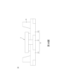
如第1圖至第4圖所示,第1圖係本申請案一實施例中所揭示之一發光元件2的上視圖。第2圖係沿著第1圖之線B-B’所揭示之發光元件2的剖面圖。第3圖係沿著第1圖之線C-C’所揭示之發光元件2的剖面圖。第4圖係第1圖所揭示之發光元件2之流程圖。As shown in FIG. 1 to FIG. 4 , FIG. 1 is a top view of a light-emitting
發光元件2包含一基板11b;一或多個半導體結構1000b位於基板11b上;一環繞部111b位於一或多個半導體結構上及/或環繞一或多個半導體結構1000a;一第一絕緣結構20b位於半導體結構1000b上,並沿著環繞部111b形成;一透明導電層30b位於一或多個半導體結構1000b上;一反射結構包含一反射層40b及一阻障層41b位於透明導電層30b上;一第二絕緣結構50b覆蓋反射層40b及阻障層41b;一接觸層60b位於第二絕緣結構50b上;一第三絕緣結構70b位於接觸層60b上;以及一第一焊墊80b和一第二焊墊90b位於接觸層60b上。The
如第1圖至第4圖所示,於發光元件2之製造流程中包含,首先在基板11b上形成半導體疊層10b。基板11b可以是藍寶石基板,但並不限於此。於一實施例中,基板11b包含一圖案化表面。圖案化表面包括複數個圖案。圖案的形狀包括圓錐(cone),角錐(pyramid)或半球形。As shown in FIGS. 1 to 4 , the manufacturing process of the light-emitting
於本申請案之一實施例中,基板11b為一成長基板,用以磊晶成長半導體疊層10b,包括用以成長磷化鋁鎵銦(AlGaInP)之砷化鎵(GaAs)晶圓,或用以成長氮化銦鎵(InGaN)之藍寶石(Al
2O
3)晶圓、氮化鎵(GaN)晶圓或碳化矽(SiC)晶圓。
In one embodiment of the present application, the
於本申請案之一實施例中,基板11b包含一圖案化表面位於半導體結構1000b和基板11b之間,其可提高發光元件之光取出效率。基板11b之裸露面可包含一圖案化表面(圖未示)。圖案化表面可為各種圖案,例如不規則圖案、微透鏡、微陣列、散射區域或其他種光學區域。例如,圖案化表面包括複數個凸部,各凸部包含一高度位於0.5〜2.5μm之間,一寬度位於1〜3.5μm之間,複數個凸部之間包含一間距(pitch)位於1〜3.5μm之間。In one embodiment of the present application, the
於本申請案之一實施例中,基板11b包含一側壁,其包含一平坦表面和/或一粗糙表面,以提高發光元件的光取出效率。於本申請案之一實施例中,基板11b的側壁係傾斜於基板11b與半導體結構1000b鄰接的一表面,以調整發光元件的光場分佈。In one embodiment of the present application, the
於本申請案之一實施例中,半導體疊層10b包括光學特性,例如發光角度或波長分佈,以及電學特性,例如正向電壓或向電流。半導體疊層10b藉由有機金屬化學氣相沉積法(MOCVD)、分子束磊晶(MBE)、氫化物氣相沉積法(HVPE)、物理氣相沉積法(PVD)或離子電鍍方法,以形成於基板11b上,其中物理氣象沉積法包含濺鍍 (Sputtering)或蒸鍍(Evoaporation)法。In one embodiment of the present application, the
一或多個半導體結構1000b各包含一半導體疊層10b,其包含一第一半導體層101b,一第二半導體層102b,及一活性層103b位於第一半導體層101b和第二半導體層102b之間。半導體結構1000b更包含一或複數個通孔100b穿過第二半導體層102b和活性層103b以露出第一半導體層101b。第一半導體層101b和第二半導體層102b可各由單層或複數個次層所構成。此外,活性層103b可為單量子井結構或者多重量子井結構。半導體疊層10b可藉由金屬有機化學氣相沉積(MOCVD),分子束磊晶(MBE)或物理氣相沉積法(PVD),在基板11b上形成III族氮化物化合物半導體層。Each of the one or
於本申請案之一實施例中,於形成半導體疊層10b之前,可先形成ㄧ緩衝結構(圖未示)於基板11b上,用以改善基板11b與半導體疊層10b之間的晶格不匹配。緩衝結構可由氮化鎵(GaN)系列之材料構成,例如氮化鎵和氮化鋁鎵,或氮化鋁(AlN)系列之材料。緩衝結構可以是單層或多層。緩衝結構可以通過金屬有機化學氣相沉積(MOCVD),分子束外延(MBE)或物理氣相沉積(PVD)來形成。物理氣相沉積(PVD)包括濺鍍(sputter)法,例如反應性濺鍍,或蒸鍍法,例如電子束蒸鍍法和熱蒸鍍法。於一實施例中,緩衝結構包括氮化鋁(AlN)緩衝層,並係由濺鍍(sputter)法形成。氮化鋁(AlN)緩衝層形成在具有圖案化表面的成長基板上。濺鍍(sputter)法可形成具有高均勻性的緻密緩衝層,因此氮化鋁(AlN)緩衝層可共形地沉積在基板11b的圖案化表面上。In one embodiment of the present application, before forming the
於本申請案之一實施例中,第一半導體層101b和第二半導體層102b,可為包覆層(cladding layer),兩者具有不同的導電型態、電性、極性,或依摻雜的元素以提供電子或電洞。例如,第一半導體層101b為n型電性的半導體層,第二半導體層102b為p型電性的半導體層。活性層103b形成在第一半導體層101b和第二半導體層102b之間,電子與電洞於一電流驅動下在活性層103b內複合,並將電能轉換成光能以發出一光線。藉由改變半導體疊層10b之一層或多層的物理及化學組成以調整發光元件2所發出光線之波長。半導體疊層10b之材料包含Ⅲ-Ⅴ族半導體材料,例如Al
xIn
yGa
(1-x-y)N或Al
xIn
yGa
(1-x-y)P,其中0≦x,y≦1;(x+y)≦1。依據活性層103b之材料,當半導體疊層10b之材料為AlInGaP系列時,活性層103b可發出波長介於610 nm及650 nm之間的紅光,或是波長介於530 nm及570 nm之間的黃光。當半導體疊層10b之材料為InGaN系列時,活性層103b可發出波長介於400 nm及490 nm之間的藍光、深藍光,或是波長介於490 nm及550 nm之間的綠光。當半導體疊層10b之材料為AlGaN系列時,活性層103b可發出波長介於250 nm及400 nm之間的紫外光。活性層103b可為單異質結構(single heterostructure, SH),雙異質結構(double heterostructure, DH),雙側雙異質結構(double-side double heterostructure, DDH),或多層量子井結構(multi-quantum well, MQW) 。活性層103b之材料可為中性、p型或n型電性的半導體。
In one embodiment of the present application, the
於半導體疊層10b形成在基板11b之後,藉由光微影(photolithography)和蝕刻工藝以圖案化半導體疊層10b,以形成複數個通孔100b以及環繞部111b。藉由光微影(photolithography)和蝕刻工藝,第二半導體層102b和活性層103b之內部的一部分被移除以形成複數個通孔100b,並且複數個通孔100b對應地裸露出第一半導體層101b的第二表面1012b。於此,通孔100b係由一內側壁1002b和第二表面1012b所定義。內側壁1002b的一端係連接至第一半導體層101b的第二表面1012b,而內側壁1002b的另一端係連接至第二半導體層102b的表面102sb。After the
於相同或另一個光微影(photolithography)和蝕刻工藝,圍繞半導體結構1000b周圍的第二半導體層102b和活性層103b被移除以形成環繞部111b,且環繞部111b露出第一半導體層101b的第一表面1011b。於另一實施例中,於光微影(photolithography)和蝕刻工藝中,第一半導體層101b之一部分進一步地被蝕刻至更深的蝕刻深度,以露出第二表面1012b和第一表面1011b。具體而言,環繞部111b包含基板11b之裸露面,第一半導體層101b露出的第一表面1011b,以及由第二半導體層102b,活性層103b和第一半導體層102b露出的側表面所構成的第一外側壁1003b和第二外側壁1001b,其中第一表面1011b之一端係連接至第一外側壁1003b,第一表面1011b之另一端係連接至第二外側壁1001b。第一外側壁1003b和第二外側壁1001b係傾斜於第一表面1011b。環繞部111b係沿著半導體結構1000b之一外圍而形成,位於及/或圍繞一或多個半導體結構1000b之外圍。於一實施例中,第一外側壁1003b傾斜於基板11b的裸露面(圖未示)。第一外側壁1003b與基板11b的裸露面之間包含一銳角。於一實施例中,第一外側壁1003b與基板11b的裸露面之間包含一鈍角。In the same or another photolithography and etching process, the
於半導體結構1000b形成之後,第一絕緣結構20b形成於半導體疊層10b上,覆蓋第二半導體層102b之表面102sb的一部份,並延伸至第二外側壁1001b,且覆蓋第一表面1011b。換言之,第一絕緣結構20b覆蓋環繞部111b之多個部分。第一絕緣結構20b保護半導體結構1000b的側壁,防止活性層103b為後續製程所破壞。如第4圖所示,於一上視圖中,第一絕緣結構20b包含一環繞絕緣部分201b以及複數個環形覆蓋區203b。於此,於一上視圖中,環繞絕緣部分201b包含複數個凸出部2011b以及複數個凹陷部2012b。複數個環形覆蓋區203b為環繞絕緣部分201b所圍繞,且複數個環形覆蓋區203b分別形成於複數個通孔100b內,並且與複數個通孔100b相對應。複數個環形覆蓋區203b中的每一個具有一開口(圖未標號)以露出第一半導體層101b的第二表面1012b。於一實施例中,第一絕緣結構20b的環繞絕緣部分201b係沿著第一半導體層101b的第一表面1011b而設置,並且圍繞半導體結構1000b。於本實施例中,環繞絕緣部分201b之複數個凸出部2011b和複數個凹陷部2012b係沿著環繞部111b交替配置,並且複數個環形覆蓋區203b的位置與複數個通孔100b的位置相對應,但是本申請案並不限於此。於一實施例中,位於兩個凸出部2011b之間的一區域構成凹陷部2012b。於另一實施例中,環繞絕緣部分201b更包含一次凸出部延伸自凸出部2011b,及/或更包括一次凹陷部自凹陷部2012b凹陷。於本實施例中,複數個凸出部2011b延伸自第二半導體層102b之上表面102sb,直接接觸並覆蓋第一半導體層101b之第一表面1011b的多個部分以及第一半導體層102b之第一表面1011b的多個角落。複數個凹陷部2012b露出未被複數個凸出部2011b所覆蓋的第一半導體層101b的第一表面1011b的其他部分。於一實施例中,複數個凹陷部2012b露出位於半導體結構1000b的複數個邊上的第一表面1011b。如第2圖所示,於一剖面圖中,第一絕緣結構20b之凹陷部2012b露出第一半導體層101b之第一表面1011b的一部分。如第3圖所示,於一剖面圖中,第一絕緣結構20b之凸出部2011b覆蓋第一半導體層101b的第一表面1011b以及半導體結構1000b的多個側壁。換言之,複數個凸出部2011b和複數個凹陷部2012b交替地覆蓋第一半導體層101b的第一表面1011b的一部分並露出第一半導體層101b的第一表面1011b的另一部分。於本實施例中,第一表面1011b的露出部分是不連續的,並且第一表面1011b的露出部分的總面積小於第一表面1011b的總面積。大部分的第二半導體層102b未被第一絕緣結構20b所覆蓋。於一上視圖中,環繞絕緣部分201b的形狀包含環狀,例如矩形、圓形或多邊形。複數個凸出部2011b或複數個凹陷部2012b之一的形狀包含三角形、矩形、半圓形、圓形或多邊形。第一絕緣結構20b的材料包含非導電材料。非導電材料包含有機材料,無機材料或是介電材料。有機材料包含Su8、苯并環丁烯(BCB)、過氟環丁烷(PFCB)、環氧樹脂(Epoxy)、丙烯酸樹脂(Acrylic Resin)、環烯烴聚合物(COC)、聚甲基丙烯酸甲酯(PMMA)、聚對苯二甲酸乙二酯(PET)、聚醯亞胺(PI)、聚碳酸酯(PC)、聚醚醯亞胺(Polyetherimide)或氟碳聚合物(Fluorocarbon Polymer)。無機材料包含矽膠(Silicone)或玻璃(Glass)。介電材料包含氧化鋁(Al
2O
3)、氮化矽(SiN
x)、氧化矽(SiO
x)、氧化鈦(TiO
x) 、或氟化鎂(MgF
x)。第一絕緣結構20b包含一層或複數層。第一絕緣結構20b可以保護半導體結構1000b的側壁,防止活性層103b為後續製程所破壞。當第一絕緣結構20b包含複數層時,第一絕緣結構20b可為包含多對膜層之布拉格反射鏡(DBR)結構以保護半導體結構1000b的側壁及選擇性地反射活性層103b所發出之特定波長之光至發光元件2之外部以提高亮度,並且每一膜層具有一折射率與相鄰膜層之折射率不同。具體而言,第一絕緣結構20b可以藉由交替堆疊SiO
x層和TiO
x層來形成。 藉由調整每對膜層之高折射率和低折射率之間的折射率差異,以使布拉格反射鏡(DBR)對特定波長或在特定波長范圍內具有高反射率。每對膜層中的兩層具有不同的厚度。每對膜層中具有相同材料的層之厚度可以相同或不同。
After the
於第一絕緣結構20b形成之後,透明導電層30b形成於第二半導體層102b上,包含複數個開口301tb以露出第一半導體層101b的第二表面1012b。於本實施例中,於一上視圖中,透明導電層30b的形狀對應於第二半導體層102b的形狀,並且複數個開口301tb的位置係對應於複數個環形覆蓋區203b和複數個通孔100b的位置。透明導電層30b接觸並覆蓋第二半導體層102b以擴散電流,並將電流注入於第二半導體層102b。此外,透明導電層30b不與第一半導體層101b相接觸。於一實施例中,發光元件2包含另一個透明導電層 (圖未標示) 與環繞部111b的第一半導體層101b相接觸。透明導電層30b的材料包括對從活性層103b所發射的光線為透明的透明材料,例如氧化銦鋅(IZO)或氧化銦錫(ITO)。透明導電層30b可與第二半導體層102b形成低電阻接觸,例如歐姆接觸(ohmic contact)。透明導電層30b包含一層或複數次層。例如,當透明導電層30b包含複數次層時,透明導電層30b可為包含複數對次層之布拉格反射鏡(DBR)結構,並且每一次層具有一折射率與相鄰次層之折射率不同。具體而言,透明導電層30b可以藉由交替堆疊具有不同折射率之兩個次層來形成布拉格反射鏡(DBR)結構。After the first
於透明導電層30b形成之後,反射結構包含反射層40b及阻障層41b對應形成於透明導電層30b上。於一實施例中,反射結構對準於透明導電層30b,反射結構的複數邊對準於透明導電層30b的複數邊。於一實施例中,反射結構不與透明導電層30b對齊,並且反射結構的複數邊位在透明導電層30b之複數邊以內或以外。於一實施例中,透明導電層30b和反射結構延伸至第一絕緣結構20b上。After the transparent
反射層40b及阻障層41b分別包含複數個開口401tb和411tb。反射層40b之複數個開口401tb及阻障層41之複數個開口411tb露出複數個環形覆蓋區203b、複數個通孔以及第一半導體層101b的第二表面1012b。阻障層41b形成並覆蓋於反射層40b上,阻障層41b可以防止反射層40b之金屬元素的遷移、擴散或氧化。反射結構之反射層40b和阻障層41b的形狀係對應於透明導電層30b的形狀。於一實施例中,反射結構之反射層40b和阻障層41b的形狀接近於矩形,並且反射層40b和阻障層41b的角落為弧形。反射層40b包含單層結構或者多層結構,並且反射層40b的材料包含對於活性層103b所發射的光線具有高反射率的金屬材料,例如銀(Ag),金(Au),鋁(Al),鈦(Ti),鉻(Cr),銅(Cu),鎳(Ni),鉑(Pt)或上述材料之合金。阻障層41b包含單層結構或多層結構,阻障層的材料包括鉻(Cr),鉑(Pt),鈦(Ti),鎢(W)或鋅(Zn)。當阻障層41b為多層結構時,阻障層41b係由第一阻障層(圖未示)和第二阻障層(圖未示)交替堆疊而形成,例如Cr/Pt,Cr/Ti,Cr/TiW,Cr/W,Cr/Zn,Ti/Pt,Ti/W,Ti/TiW,Ti/Zn,Pt/TiW,Pt/W,Pt/Zn,TiW/W,TiW/Zn,或W/Zn。反射結構可更包含一布拉格反射鏡(DBR)形成在反射層40b之下。布拉格反射鏡(DBR)結構包含複數對次層,並且每一次層具有一折射率與相鄰次層的折射率不同。於一實施例中,複數對次層可以藉由交替堆疊SiO
x層和TiO
x層來形成。藉由調整每對次層之高折射率和低折射率之間的折射率差異,以使布拉格反射鏡(DBR)對特定波長或在特定波長范圍內具有高反射率。每對次層之其中兩層具有不同的厚度。每對次層中具有相同材料之層的厚度可以相同或不同。
The
於反射結構形成之後,第二絕緣結構50b形成在反射結構上以覆蓋反射結構(反射層40b或阻障層41b)之上表面的一部分,並且位於反射結構與第一絕緣結構20b之間的第二半導體層102b的周圍區域。第二絕緣結構50b接觸並覆蓋第一絕緣結構20b,使得環繞部111b之第一外側壁1003b和第二外側壁1001b以及為第一絕緣結構20b所覆蓋之第一表面1011b之部分亦被第二絕緣結構50b所覆蓋。第二絕緣結構50b可保護半導體結構1000b的側壁,防止活性層103b為後續製程所破壞。由於第二絕緣結構50b覆蓋第一絕緣結構20b,因此第二絕緣結構50b能夠防止第一絕緣結構20b於後續製程中被蝕刻移除。如第4圖所示,第二絕緣結構50b包含複數個開口501b以及一開口503b。於此,第二絕緣結構50b包含一外圍505b具有複數個凸出部5051b和複數個凹陷部5052b。開口503b露出反射結構之反射層40b或阻障層41b的一部分,並且複數個開口501b露出第一半導體層101b的第二表面1012b。如第2圖至第4圖所示,於本實施例中,第二絕緣結構50b的外圍505b接觸、覆蓋並對齊於第一絕緣結構20b。複數個開口501b的位置與複數開口401tb,411tb,301tb,以及複數個通孔100b的位置對應。此外,位於第二絕緣結構50b外圍505b的複數個凸出部5051b和複數個凹陷部5052b沿著第一絕緣結構20b的環繞絕緣部分201b或環繞部111b交替排列以分別覆蓋及暴露第一半導體層101b的第一表面1011b的不同部份。於一實施例中,位於兩個凸出部5051b之間的區域構成凹陷部5052b。於另一實施例中,第二絕緣結構50b更包含一次凸出部延伸自凸出部5051b,及/或更包括一次凹陷部自凹陷部5052b凹陷。此外,於一實施例中,第二絕緣結構50b之外圍505b的形狀係對應於第一絕緣結構20b之環繞絕緣部分201b的形狀,用以不連續地露出位於環繞部111b上的第一半導體層101b的第一表面1011b之部份。換言之,複數個凸出部5051b和複數個凹陷部5052b的形狀和位置係對應於環繞絕緣部分201b之複數個凸出部2011b和複數個凹陷部2012b的形狀和位置。為複數個凹陷部2012b所露出的第一表面1011b之部份亦為多個複數個凹陷部5052b所露出。為複數個凸出部2011b所覆蓋的第一表面1011b之部份亦為複數個凸出部5051b所覆蓋。當第一表面1011b為第一絕緣結構20b和第二絕緣結構50b所不連續地露出時,於一實施例中,凸出部5051b和凹陷部5052b的形狀或位置可與凸出部2011b和凹陷部2012b的形狀或位置不同。於一實施例中,凸出部5051b和凹陷部5052b的面積可大於或小於凸出部2011b和凹陷部2012b的面積。為凹陷部2012b及凹陷部5052b所露出的第一表面1011b的部份係藉由凸出部2011b, 5051b和凹陷部2012b, 5052b的形狀、位置或面積來調整。After the reflective structure is formed, the second
如第2圖所示,於一剖面圖中,第一半導體層101b之第一表面1011b的一部分為第一絕緣結構20b之複數個凹陷部2012b所露出,並且為第二絕緣結構50b之複數個凹陷部5052b所露出。換言之,第二絕緣結構50b之複數個凹陷部5052b露出第一半導體層101b之第一表面1011b上未被複數個凸出部2011b,5051b覆蓋並且為複數個凹陷部2012b所露出的部分。如第3圖所示,於一剖面圖中,複數個凸出部5051b於第一半導體層101b之第一表面1011b上覆蓋第一絕緣結構20b的複數個凸出部2011b,並且覆蓋形成在第一外側壁1003b和第二外側壁1001b上的環繞絕緣部分201b以及第一半導體層101b之第一表面1011b的角落,其中第一外側壁1003b和第二外側壁1001b係由第二半導體層102b,活性層103b和第一半導體層101b所露出的側表面所構成。具體而言,於本實施例中,複數個凸出部5051b直接接觸第一絕緣結構20b之複數個凸出部2011b,複數個凹陷部5052b露出第一半導體層101b之第一表面1011b,且複數個凸出部5051b及複數個凹陷部5052b彼此交替排列以不連續地露出第一半導體層101b的第一表面1011b的部份。換言之,為複數個凹陷部5052b所露出的第一表面1011b的部份係不連續的,並且第一表面1011b具有一總裸露面積。第一表面1011b之總裸露面積係小於第一表面1011b之整體面積。As shown in FIG. 2, in a cross-sectional view, a part of the
於一實施例中,複數個凸出部5051b之一的形狀包含三角形、矩形、半圓形、圓形或多邊形。第二絕緣結構50b的材料包含非導電材料。非導電材料包含有機材料,無機材料或介電材料。有機材料包含Su8、苯并環丁烯(BCB)、過氟環丁烷(PFCB)、環氧樹脂(Epoxy)、丙烯酸樹脂(Acrylic Resin)、環烯烴聚合物(COC)、聚甲基丙烯酸甲酯(PMMA)、聚對苯二甲酸乙二酯(PET)、聚醯亞胺(PI)、聚碳酸酯(PC)、聚醚醯亞胺(Polyetherimide)或氟碳聚合物(Fluorocarbon Polymer)。無機材料包含矽膠(Silicone)或玻璃(Glass)。介電材料包含氧化鋁(Al
2O
3)、氮化矽(SiN
x)、氧化矽(SiO
x)、氧化鈦(TiO
x) 、或氟化鎂(MgF
x)。第二絕緣結構50b包含一層或複數層。第二絕緣結構50b可保護半導體結構1000b的側壁,防止活性層103b為後續製程所破壞,以及選擇性地反射活性層103b所發出之特定波長之光至發光元件2之外部以提高亮度。當第二絕緣結構50b包含複數層時,第二絕緣結構50b可為包含多對膜層之布拉格反射鏡(DBR)結構,並且每一膜層具有一折射率與相鄰膜層之折射率不同。於一實施例中,第二絕緣結構50b可以藉由交替堆疊SiO
x層和TiO
x層來形成。 藉由調整每對膜層之高折射率和低折射率之間的折射率差異,以使布拉格反射鏡(DBR)對特定波長或在特定波長范圍內具有高反射率。每對膜層中的兩層具有不同的厚度。每對膜層中具有相同材料的層的厚度可以相同或不同。
In one embodiment, the shape of one of the plurality of
參考第1圖至第4圖,接觸層60b位於第二絕緣結構50b及反射結構(反射層40b及阻障層41b)上,包含一第一接觸部分600b,一第二接觸部分601b及一第三接觸部分602b。於一實施例中,其中於一上視圖下,第二接觸部分601b位於半導體結構之一幾何中心上。第一接觸部分600b及第三接觸部分602b係彼此分離。第三接觸部分602b為第一接觸部分600b所圍繞。第一接觸部分600b係電連接至第一半導體層101b,第三接觸部分602b係電連接至第二半導體層102b,且第二接觸部分601b係與第一半導體層101b及第二半導體層102b電性絕緣。於一實施例中,第二接觸部分601b電連接至第一接觸部分600b及第三接觸部分602b之其中之一。於一實施例中,第一接觸部分600b藉由第二絕緣結構50b之複數個開口501b及複數個凹陷部5052b以接觸第二表面1012b及第一表面1011b,並電連接至第一半導體層101b。此外,於環繞部111b之一剖面圖中,第一接觸部分600b沿著第一絕緣結構20b或第二絕緣結構50b之一外圍505b具有一凹凸上表面。第一接觸部分600b沿著外圍505b而形成在複數個凸出部5051b和複數個凹陷部5052b上,並且凹凸上表面係對應於複數個凸出部5051b和複數個凹陷部5052b而形成。第一接觸部分600b藉由環繞絕緣部分201b之複數個凹陷部2012b及第二絕緣結構50b之複數個凹陷部5052b以不連續地接觸第一表面1011b。第一接觸部分600b與第一半導體層101b之第一表面1011b包含複數個不連續的第一接觸區域(圖未示)。第一接觸部分600b與第一半導體層101b之第二表面1012b包含複數個第一接觸區域(圖未示)。1 to 4, the
於本實施例中,第二接觸部分601b及第三接觸部分602b為第一接觸部分600b所環繞,並且於一上視圖中,第二接觸部分601b的形狀包含一幾何形狀,例如矩形、圓形或不規則形。第三接觸部分602b藉由第二絕緣結構50b之開口503b以接觸反射結構並電連接至第二半導體層102b。第三接觸部分602b與反射結構之間具有一第二接觸區域(圖未示)。於一實施例中,第二接觸部分601b可連接至第一接觸部分600b或第三接觸部分602b。接觸層60b可為單層或複數個次層組成。接觸層60b包含金屬材料,例如鋁(Al),鉻(Cr),鉑(Pt),鈦(Ti),鎢(W)或鋅(Zn)。In this embodiment, the
參考第1圖至第4圖,於接觸層60b形成之後,第三絕緣結構70b形成在接觸層60b上並覆蓋接觸層60b。第三絕緣結構70b包含一第一開口701b及一第二開口702b。第三絕緣結構70b之第一開口701b露出接觸層60b之第一接觸部分600b。第二開口702b露出接觸層60b之第三接觸部分602b。第三絕緣結構70b的材料包含非導電材料。非導電材料包含有機材料,無機材料或是介電材料。有機材料包含Su8、苯并環丁烯(BCB)、過氟環丁烷(PFCB)、環氧樹脂(Epoxy)、丙烯酸樹脂(Acrylic Resin)、環烯烴聚合物(COC)、聚甲基丙烯酸甲酯(PMMA)、聚對苯二甲酸乙二酯(PET)、聚醯亞胺(PI)、聚碳酸酯(PC)、聚醚醯亞胺(Polyetherimide)或氟碳聚合物(Fluorocarbon Polymer)。無機材料包含矽膠(Silicone)或玻璃(Glass)。介電材料包含氧化鋁(Al
2O
3)、氮化矽(SiN
x)、氧化矽(SiO
x)、氧化鈦(TiO
x) 、或氟化鎂(MgF
x)。第一絕緣結構20b,第二絕緣結構50b及第三絕緣結構70b可藉由網印,蒸鍍或濺鍍而形成。
Referring to FIGS. 1 to 4, after the
於第三絕緣結構70b形成之後,第一焊墊80b和第二焊墊90b形成在半導體疊層10b上以完成發光元件2之製造。第一焊墊80b及第二焊墊90b的位置係分別對應於第三絕緣結構70b之第一開口701b及第二開口702b的位置。於一實施例中,第一焊墊80b及第二焊墊90b之位置及形狀係分別對應於第三絕緣結構70b之第一開口701b及第二開口702b之位置及形狀。第一焊墊80b藉由第三絕緣結構70b之第一開口701b以與接觸層60b之第一接觸部分600b相接觸,並電連接至第一半導體層101b。第二焊墊90b藉由第三絕緣結構70b之第二開口702b以與接觸層60b之第三接觸部分602b相接觸,並電連接至第二半導體層102b。於一實施例中,由發光元件之一上視圖觀之,第一焊墊80b包含與第二焊墊90b相同之形狀,例如第一焊墊80b及第二焊墊90b包含梳狀,但發明並不限於此。於一實施例中,第一焊墊80b之形狀或大小可與第二焊墊90b之形狀或大小不同。例如,第一焊墊80b之形狀為矩形,第二焊墊90b之形狀為梳狀,且第一焊墊80b之面積大於第二焊墊90b之面積。於一實施例中,第一焊墊80b和第二焊墊90b包含一結構具有單層或複數層。第一焊墊80b和第二焊墊90b包含金屬材料,例如鉻(Cr),鈦(Ti),鎢(W),鋁(Al),銦(In),錫(Sn),鎳(Ni),鉑(Pt)或上述材料之合金。當第一焊墊80b和第二焊墊90b包含複數層時,第一焊墊80b包含一第一上焊墊和第一下焊墊,並且第二焊墊90b包括第二上焊墊和第二下焊墊。上焊墊和下焊墊具有不同的功能。上焊墊的功能係用於焊接和接線。發光元件2可藉由上焊墊透過焊料(solder)或AuSn共晶接合、翻轉並安裝至一封裝基板上。上焊墊包含一具有高延展性的金屬材料,例如鎳(Ni),鈷(Co),鐵(Fe),鈦(Ti),銅(Cu),金(Au),鎢(W),鋯(Zr),鉬(Mo),鉭(Ta),鋁(Al),銀(Ag),鉑(Pt),鈀(Pd),銠(Rh),銥(Ir),釕(Ru),鋨(Os)。上焊墊可以是上述材料的單層,多層或合金。於本申請案之一實施例中,上焊墊之材料較佳的包含鎳(Ni)及/或金(Au),且上焊墊可為單層或多層。下焊墊的功能是與接觸層60b、反射層40b或阻障層41b形成穩定介面,例如改善第一下焊墊和接觸層60b之間的介面接合強度,或改善第二下焊墊與反射層40b或阻障層41b之間的介面接合強度。下焊墊的另一個功能是防止焊料或AuSn中的錫(Sn)擴散至反射結構中,破壞反射結構的反射率。因此,下焊墊較佳的包含金(Au)和銅(Cu)以外的金屬元素,例如鎳(Ni),鈷(Co),鐵(Fe),鈦(Ti),鎢(W),鋯(Zr),鉬(Mo),鉭(Ta),鋁(Al),銀(Ag),鉑(Pt),鈀(Pd),銠(Rh),銥(Ir),釕(Ru),鋨(Os)。下焊墊可以是上述材料的單層,多層或合金。於本申請案之一實施例中,下焊墊較佳的包括鈦(Ti)和鋁(Al)的多層膜,或鉻(Cr)和鋁(Al)的多層膜。After the third
於一實施例中,當操作發光元件2之時,一外部電源分別電連接至第一焊墊80b和第二焊墊90b。此時電流被注入至發光元件2中,藉由第一接觸部分600b和第三接觸部分602b以擴散電流,分別經由第一接觸區域和第二接觸區域注入第一半導體層101b和第二半導體層102b中。為了改善發光元件2之電流分佈,可以調整第一接觸部分600b以及第一半導體層101b的第一表面1011b之間的第一接觸區域的面積和位置,避免電流集中於第一表面1011b的某些區域,例如第一表面1011b的角落。於一實施例中,由於第一絕緣結構20b的環繞絕緣部分201b和第二絕緣結構50b的外圍505b覆蓋第一半導體層101b之第一表面1011b的一部分,所以接觸層60b和第一表面1011b間之第一接觸區域的面積和位置可藉由環繞絕緣部分201b和第二絕緣結構50b來調整。換言之,第一接觸區域的面積和位置係藉由環繞絕緣部分201b和第二絕緣結構50b的凹陷部2012b,5052b所露出的第一表面1011b之露出部分來調整。然而,在設計第一絕緣結構20b的環繞絕緣部分201b和第二絕緣結構50b時,發光元件2的正向電壓(V
f)和電流分佈必須同時考慮有所取捨。具體而言,第一接觸區域的面積越大,發光元件2的正向電壓越低。然而,若第一接觸區域的面積越大,發光元件2將產生電流壅塞效應。為了達到可接受的正向電壓(V
f)和較佳的電流分佈,第一接觸部分600b被設計藉由複數個凹陷部2012b,5052b以不連續地接觸第一表面1011b,藉由複數個凸出部2011b,5051b以與第一表面1011b的部份電性絕緣。於一實施例中,第一接觸部分600b被設計成避免接觸第一半導體層101b之第一表面1011b的角落。依此,電流藉由第一接觸部分600b之不連續的第一接觸區域而注入至第一半導體層101b,且不能直接注入至為第一絕緣結構20b和第二絕緣結構50b所覆蓋的區域中。因此,電流可以藉由第一接觸部分600b擴散,並進一步藉由不連續的第一接觸區域擴散。換言之,環繞絕緣部分201b和第二絕緣結構50b的外圍505b設計可影響正向電壓值,並改變電流路徑,迫使電流流入為複數個凹陷部2012b及複數個凹陷部5052b所露出的第一表面,改變電流分布。於本實施例中,第一接觸部分600b的面積足夠以達到可接受的正向電壓值,例如2.15 V~2.4 V,並且在此第一接觸區域下可以達到期望的電流分佈,細節將於下描述。
In one embodiment, when operating the light-emitting
如第5圖和第6圖所示,第5圖係發光元件2之燒毀區域的上視圖。第6圖係習知發光元件3之燒毀區域的上視圖。發光元件2與傳統的發光元件3之間的差異在於傳統發光元件3的第一絕緣結構20b'與第二絕緣結構50b'不具有如發光元件2的複數個凸出部2011b,5051b和複數個凹陷部2012b,5052b。在傳統發光元件3中,第一半導體層101b的第一表面1011b整體被暴露以與接觸層60b接觸,使得接觸層60b係連續的接觸第一半導體層101b的第一表面1011b,並且直接接觸第一半導體層101b之第一表面1011b的角落(圖未標示)。As shown in FIG. 5 and FIG. 6 , FIG. 5 is a top view of the burnt area of the
如第6圖所示,當傳統的發光元件3被施以一突波時,傳統的發光元件3無法承受此高電壓並有效地分散電流,使電流集中於角落,因此傳統的發光元件3容易燒毀。參考第6圖,突波之電壓超過傳統發光件3的正常工作電壓,並且此突波藉由標號為f3的多個故障區域以燒毀傳統的發光元件3。相較於其他區域,傳統發光件3的的電流更傾向於聚集在角落處。當發光元件2被施以一超過其可承受的突波時,如第5圖所示,發光元件2之故障區域標號為f2。故障區域f2的分佈與傳統發光元件3的故障區域f3的分佈不同,發光元件2的電流未聚集在第一半導體層101b之第一表面1011b的角落,發光元件2的電流分佈比傳統的發光元件3的電流分佈更均勻,並可承受更高電壓的突波。As shown in Figure 6, when a surge is applied to the traditional light-emitting
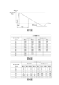
於本實施例中,接觸層60b與第一半導體層101b之第一表面1011b間的不連續第一接觸區有益於發光元件2的電流擴散,並且避免發光元件2被擊穿(breakdown)。此外,藉由不連續的第一接觸區,發光元件2具有可接受的正向電壓,例如,2.15V-2.4V,和預期的的電流分佈。於一實施例中,發光元件2和傳統的發光元件3在不同施加電壓下進行過度電性應力(Electrical Over Stress, EOS)測試。請參考第7圖、第8圖和第9圖。第7圖係一突波(surge)於過度電性應力(Electrical Over Stress, EOS)測試下之電壓波型圖。第8圖係發光元件2與習知發光元件3於過度電性應力(Electrical Over Stress, EOS)測試下,最大施加電壓之突波(surge)對可導通之正向電壓(forward voltage, V
f)之一圖表。第9圖係發光元件2與習知發光元件3於過度電性應力(Electrical Over Stress, EOS)測試下,突波(surge)之最大施加電壓對反向電流(reverse current, I
r)之一圖表。為了進一步比較本申請案之發光元件2和傳統的發光元件3,如第8圖所示,發光元件2的樣品1,2和傳統發光元件3的樣品1,2於過度電性應力(Electrical Over Stress, EOS)測試。在EOS測試中(符合IEC 61000-4-5標準),如第7圖所示,具有一電壓波形之突波分別施加到發光元件2和傳統的發光元件3。每一突波的電壓隨時間而變化,並且每一突波具有一最大施加電壓Va(max)。如第8圖所示,多個樣品被施以不同的最大施加電壓Va(max),例如0V,20V,30V,35V,40V,45V,50V,55V,60V和65V。對每一最大施加電壓Va(max),以每秒1次的頻率施加5次突波,每一突波約持續10
-4秒。每一樣品的大小約為38Í38 mil
2。經最大施加電壓進行突波測試之後,在固定電流10μA下驅動每個樣品,測量每個樣品的正向電壓(V
f)並記錄於第8圖的表格中。如第8圖所示,發光元件2的樣品1,2分別在最大施加電壓65V和60V的突波下進行EOS測試,其所測量到的正向電壓Vf小於2.15V。傳統發光元件3的樣品1,2在最大施加電壓50V的突波下進行EOS測試,其所測量到的正向電壓Vf小於2.15V。此外,由於可接受的正向電壓值在2.15V和2.4V之間,發光元件2的樣品1在施加等於或小於60V的最大施加電壓的突波之後,所測量到的正向電壓大於2.15 V及小於2.4 V,即發光元件2的樣品1於EOS測試之後仍能正常操作。發光元件2的樣品2在施加等於或小於55V的最大施加電壓的突波之後,所測量到的正向電壓大於2.15 V及小於2.4 V,即樣品2於EOS測試之後仍能正常操作。相較於傳統的發光元件3,發光元件2可承受60V的最大施加電壓的突波,因此發光元件2於過度電性應力(Electrical Over Stress, EOS)測試中的表現比傳統的發光元件3佳。
In this embodiment, the discontinuous first contact region between the
於一實施例中,與上述實施例類似,如第9圖所示,將發光元件2之樣品1,2,3,4以及習知之發光元件3之樣品1,2,3,4用於過度電性應力(Electrical Over Stress, EOS)測試。藉由施加不同的最大電壓0V,60V,65V,70V,75V和80V以對每一樣品施以一突波(surge)測試。經施以最大電壓後的突波(surge)測試之後,於反向電壓-5V下驅動樣品,並測量每一樣品的反向電流(Ir),將測量值紀錄於第9圖中。於本實施例中,發光元件之可接受的反向電流(Ir)係小於0.3μA。如第9圖所示,當發光元件受到損傷,例如擊穿,則反向電流(Ir)將會發生,且在本實施例會被量測到如第9圖所示的100 μA的讀值。在最大施加電壓75V和80V的突波(surge)下進行過度電性應力(Electrical Over Stress, EOS)測試,發光元件2之樣品1,2,3,4的反向電流Ir(μA)為100 μA大於0.3μA。換言之,發光元件2可承受之突波(surge)的最大施加電壓在75V以下。在最大施加電壓65V至80V的突波(surge)下進行過度電性應力(Electrical Over Stress, EOS)測試,發光元件3之樣品1,2,3,4的反向電流Ir(μA)大於0.3μA。換言之,發光元件3可承受之突波(surge)的最大施加電壓在65V以下。此外,由於可接受的反向電流(Ir)小於0.3μA,在施以等於或小於70V之最大施加電壓的突波(surge)之後,發光元件2之樣品1,2,3,4的測試結果顯示反向電流Ir為零,即發光元件2之樣品1,2,3,4仍可正常操作並通過過度電性應力(Electrical Over Stress, EOS)測試。相較於發光元件3,發光元件2可承受70V的最大施加電壓,因此發光元件2於過度電性應力(Electrical Over Stress, EOS)測試中的表現比傳統的發光元件3佳。In one embodiment, similar to the above-mentioned embodiment, as shown in FIG. Electrical Over Stress (EOS) test. Each sample was subjected to a surge test by applying different maximum voltages of 0V, 60V, 65V, 70V, 75V and 80V. After the surge test after the maximum voltage was applied, the samples were driven at a reverse voltage of -5V, and the reverse current (Ir) of each sample was measured, and the measured values were recorded in Figure 9. In this embodiment, the acceptable reverse current (Ir) of the light emitting device is less than 0.3 μA. As shown in FIG. 9, when the light-emitting element is damaged, such as breakdown, a reverse current (Ir) will occur, and in this embodiment, a reading value of 100 μA as shown in FIG. 9 will be measured. The electrical over stress (EOS) test was carried out under the surge of the maximum applied voltage of 75V and 80V, and the reverse current Ir (μA) of the
如第8圖及第9圖所示,發光元件2在過度電性應力(Electrical Over Stress, EOS)測試下的可靠度優於傳統的發光元件3。於本申請案之實施例中,藉由第一絕緣結構之環繞絕緣部分201b和第二絕緣結構50b之外圍505b設計,本申請案之發光元件2可避免電流集中於角落。並且,可藉由調整接觸層60b之第一接觸區域的面積和位置,以達到可接受的正向電壓。藉此可以達到2.15 V-2.4 V之間的正向電壓,改善發光元件2的電流分佈,提高發光元件2的可靠度。As shown in FIG. 8 and FIG. 9 , the reliability of the light-emitting
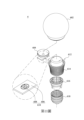
第10圖係為依本申請案一實施例之發光裝置30之示意圖。將前述實施例中的發光元件2以倒裝晶片之形式安裝於封裝基板51之第一墊片511、第二墊片512上。第一墊片511、第二墊片512之間藉由一包含絕緣材料之絕緣部53做電性絕緣。倒裝晶片之安裝係將與焊墊形成面相對之成長基板11b側朝上設置,使成長基板側為主要的光取出面。為了增加發光裝置30之光取出效率,可於發光元件2之周圍設置一反射結構54。FIG. 10 is a schematic diagram of a
第11圖係為依本申請案一實施例之發光裝置4之示意圖。發光裝置4為一球泡燈包括一燈罩602、一反射鏡604、一發光模組610、一燈座612、一散熱片614、一連接部616以及一電連接元件618。發光模組610包含一承載部606,以及複數個發光單元608位於承載部606上,其中複數個發光單元608可為前述實施例中的發光元件2或發光裝置30。Fig. 11 is a schematic diagram of a
本申請案所列舉之各實施例僅用以說明本申請案,並非用以限制本申請案之範圍。任何人對本申請案所作之任何顯而易知之修飾或變更皆不脫離本申請案之精神與範圍。The various embodiments listed in this application are only used to illustrate this application, and are not intended to limit the scope of this application. Any obvious modifications or changes made by anyone to this application do not depart from the spirit and scope of this application.
2 發光元件2 light emitting elements
3 傳統發光元件3 Traditional light-emitting components
4 發光裝置4 Lighting device
10b 半導體疊層10b Semiconductor stack
11b 基板11b Substrate
20b、20b' 第一絕緣結構20b, 20b' first insulating structure
30 發光裝置30 light emitting device
30b 透明導電層30b transparent conductive layer
40b 反射層40b reflective layer
41b 阻障層41b Barrier layer
50b、 50b' 第二絕緣結構50b, 50b' second insulating structure
60b 接觸層60b contact layer
60b' 接觸層60b' contact layer
70b 第三絕緣結構70b Third insulation structure
80b 第一焊墊80b First pad
90b 第二焊墊90b Second welding pad
100b 通孔100b through hole
101b 第一半導體層101b first semiconductor layer
102b 第二半導體層102b second semiconductor layer
102sb 表面102sb surface
103b 活性層103b active layer
111b 環繞部111b Surrounding part
201b 環繞絕緣部分201b Surrounding insulation
203b 環形覆蓋區203b Ring coverage area
301tb 開口301tb opening
401tb 開口401tb opening
411tb 開口411tb opening
501b 開口501b opening
503b 開口503b opening
505b 外圍505b peripheral
600b 第一接觸部分600b first contact part
601b 第二接觸部分601b Second contact part
602b 第三接觸部分602b Third contact part
701b 第一開口701b First opening
702b 第二開口702b Second opening
1000b 半導體結構1000b Semiconductor Structures
1002b 內側壁1002b inner wall
1001b 第二外側壁1001b second outer wall
1003b 第一外側壁1003b first outer wall
1011b 第一表面1011b first surface
1012b 第二表面1012b second surface
2011b 凸出部2011b Protrusion
2012b 凹陷部2012b Depression
5051b 凸出部5051b Protrusion
5052b 凹陷部5052b Depression
f2 故障區域f2 fault area
f3 故障區域f3 fault area
51 封裝基板51 package substrate
53 絕緣部53 insulation part
54 反射結構54 Reflective structure
511 第一墊片511 first gasket
512 第二墊片512 second gasket
602 燈罩602 lampshade
604 反射鏡604 reflector
606 承載部606 Carrying part
608 發光單元608 light emitting unit
610 發光模組610 Lighting Module
612 燈座612 lamp holder
614 散熱片614 heat sink
616 連接部616 connection part
618 電連接元件618 Electrical connection components
第1圖係本申請案一實施例中所揭示之一發光元件2的上視圖。FIG. 1 is a top view of a
第2圖係沿著第1圖之線B-B’所揭示之發光元件2的剖面圖。Fig. 2 is a cross-sectional view of the light-emitting
第3圖係沿著第1圖之線C-C’所揭示之發光元件2的剖面圖。Fig. 3 is a cross-sectional view of the light-emitting
第4圖係第1圖所揭示之發光元件2之各層上視圖。Fig. 4 is a top view of each layer of the light-emitting
第5圖係本申請案一實施例中所揭示之發光元件2之燒毀區域的上視圖。FIG. 5 is a top view of the burnt area of the light-emitting
第6圖係傳統發光元件3之燒毀區域的上視圖。FIG. 6 is a top view of the burnt area of a conventional light-emitting
第7圖係一突波(surge)於過度電性應力(Electrical Over Stress, EOS)測試下之電壓波型圖。Figure 7 is a voltage waveform diagram of a surge under the Electrical Over Stress (EOS) test.
第8圖係突波(surge)之最大施加電壓對可導通之正向電壓(forward voltage, V f)之一圖表。 Fig. 8 is a graph of the maximum applied voltage of a surge versus the forward voltage (V f ) that can be turned on.
第9圖係突波(surge)之最大施加電壓對反向電流(reverse current, I r)之一圖表。 Fig. 9 is a graph of the maximum applied voltage of a surge versus the reverse current (I r ).
第10圖係為依本申請案一實施例之發光裝置30之示意圖。FIG. 10 is a schematic diagram of a
第11圖係為依本申請案一實施例之發光裝置4之示意圖。Fig. 11 is a schematic diagram of a
無。none.
2 發光元件
10b 半導體疊層
11b 基板
20b 第一絕緣結構
30 發光裝置
30b 透明導電層
40b 反射層
41b 阻障層
50b 第二絕緣結構
70b 第三絕緣結構
80b 第一焊墊
90b 第二焊墊
100b 通孔
101b 第一半導體層
102b 第二半導體層
102sb 表面
103b 活性層
111b 環繞部
600b 第一接觸部分
601b 第二接觸部分
602b 第三接觸部分
1000b 半導體結構
1002b 內側壁
1001b 第二外側壁
1003b 第一外側壁
1011b 第一表面
2
Claims (10)
Applications Claiming Priority (2)
| Application Number | Priority Date | Filing Date | Title |
|---|---|---|---|
| US201762450860P | 2017-01-26 | 2017-01-26 | |
| US62/450,860 | 2017-01-26 |
Publications (2)
| Publication Number | Publication Date |
|---|---|
| TW202247497A TW202247497A (en) | 2022-12-01 |
| TWI790984B true TWI790984B (en) | 2023-01-21 |
Family
ID=62813050
Family Applications (7)
| Application Number | Title | Priority Date | Filing Date |
|---|---|---|---|
| TW111131100A TWI790984B (en) | 2017-01-26 | 2018-01-17 | Light-emitting device |
| TW107101738A TWI778010B (en) | 2017-01-26 | 2018-01-17 | Light-emitting device |
| TW107102143A TWI758400B (en) | 2017-01-26 | 2018-01-22 | Light-emitting device |
| TW111104714A TWI795205B (en) | 2017-01-26 | 2018-01-22 | Light-emitting device |
| TW112127195A TW202343836A (en) | 2017-01-26 | 2018-01-25 | Light-emitting device |
| TW107102755A TWI758402B (en) | 2017-01-26 | 2018-01-25 | Light-emitting device |
| TW111105545A TWI813171B (en) | 2017-01-26 | 2018-01-25 | Light-emitting device |
Family Applications After (6)
| Application Number | Title | Priority Date | Filing Date |
|---|---|---|---|
| TW107101738A TWI778010B (en) | 2017-01-26 | 2018-01-17 | Light-emitting device |
| TW107102143A TWI758400B (en) | 2017-01-26 | 2018-01-22 | Light-emitting device |
| TW111104714A TWI795205B (en) | 2017-01-26 | 2018-01-22 | Light-emitting device |
| TW112127195A TW202343836A (en) | 2017-01-26 | 2018-01-25 | Light-emitting device |
| TW107102755A TWI758402B (en) | 2017-01-26 | 2018-01-25 | Light-emitting device |
| TW111105545A TWI813171B (en) | 2017-01-26 | 2018-01-25 | Light-emitting device |
Country Status (6)
| Country | Link |
|---|---|
| US (10) | US10340423B2 (en) |
| JP (4) | JP7246853B2 (en) |
| KR (5) | KR102494108B1 (en) |
| CN (6) | CN108365068B (en) |
| DE (1) | DE102018101658A1 (en) |
| TW (7) | TWI790984B (en) |
Families Citing this family (15)
| Publication number | Priority date | Publication date | Assignee | Title |
|---|---|---|---|---|
| TWI790984B (en) * | 2017-01-26 | 2023-01-21 | 晶元光電股份有限公司 | Light-emitting device |
| JP7100980B2 (en) | 2018-01-22 | 2022-07-14 | ローム株式会社 | LED package |
| DE102018101393A1 (en) * | 2018-01-23 | 2019-07-25 | Osram Opto Semiconductors Gmbh | OPTOELECTRONIC SEMICONDUCTOR CHIP AND METHOD FOR PRODUCING AN OPTOELECTRONIC SEMICONDUCTOR CHIP |
| US20190237629A1 (en) * | 2018-01-26 | 2019-08-01 | Lumileds Llc | Optically transparent adhesion layer to connect noble metals to oxides |
| US11038085B2 (en) * | 2018-08-01 | 2021-06-15 | Epistar Corporation | Light-emitting device with a plurality of electrodes on a semiconductor stack |
| CN110828502B (en) * | 2018-08-09 | 2024-04-02 | 首尔伟傲世有限公司 | Light-emitting element |
| CN109860366A (en) * | 2018-12-28 | 2019-06-07 | 映瑞光电科技(上海)有限公司 | Flip LED chips |
| CN109728140A (en) * | 2018-12-28 | 2019-05-07 | 映瑞光电科技(上海)有限公司 | A kind of high pressure flip LED chips and forming method thereof |
| US10971650B2 (en) | 2019-07-29 | 2021-04-06 | Lextar Electronics Corporation | Light emitting device |
| US11764328B2 (en) * | 2019-08-13 | 2023-09-19 | Epistar Corporation | Light-emitting diode package having bump formed in wriggle shape |
| US11594658B2 (en) * | 2020-03-06 | 2023-02-28 | Lextar Electronics Corporation | Flip-chip light emitting diode with two flat pads |
| TWI726685B (en) | 2020-04-16 | 2021-05-01 | 錼創顯示科技股份有限公司 | Micro light-emitting device display apparatus |
| CN114188448A (en) * | 2020-09-14 | 2022-03-15 | 厦门乾照光电股份有限公司 | LED chip and manufacturing method thereof |
| CN115528154A (en) * | 2021-09-07 | 2022-12-27 | 厦门三安光电有限公司 | Flip-chip light emitting diode and light emitting device |
| US20240063344A1 (en) * | 2022-08-17 | 2024-02-22 | Creeled, Inc. | Metallic layer for dimming light-emitting diode chips |
Citations (2)
| Publication number | Priority date | Publication date | Assignee | Title |
|---|---|---|---|---|
| TW201603319A (en) * | 2014-07-03 | 2016-01-16 | 晶元光電股份有限公司 | Optoelectronic device and method for manufacturing the same |
| TW201633563A (en) * | 2014-12-16 | 2016-09-16 | 晶元光電股份有限公司 | Light-emitting element |
Family Cites Families (61)
| Publication number | Priority date | Publication date | Assignee | Title |
|---|---|---|---|---|
| JPH07193279A (en) * | 1993-12-27 | 1995-07-28 | Stanley Electric Co Ltd | Optical semiconductor device |
| JP4201079B2 (en) * | 2002-12-20 | 2008-12-24 | 昭和電工株式会社 | LIGHT EMITTING ELEMENT, MANUFACTURING METHOD THEREOF, AND LED LAMP |
| JP5008263B2 (en) | 2005-03-02 | 2012-08-22 | 日亜化学工業株式会社 | Semiconductor light emitting device |
| JP2009176900A (en) * | 2008-01-23 | 2009-08-06 | Mitsubishi Electric Corp | Semiconductor light-emitting element and method of manufacturing the same |
| JP5426124B2 (en) * | 2008-08-28 | 2014-02-26 | 株式会社東芝 | Semiconductor light emitting device manufacturing method and semiconductor light emitting device |
| JP2010157547A (en) * | 2008-12-26 | 2010-07-15 | Showa Denko Kk | Method of manufacturing silicon carbide semiconductor device |
| WO2010114250A2 (en) * | 2009-03-31 | 2010-10-07 | Seoul Semiconductor Co., Ltd. | Light emitting device having plurality of light emitting cells and method of fabricating the same |
| JP2011071272A (en) * | 2009-09-25 | 2011-04-07 | Toshiba Corp | Semiconductor light-emitting device and method for manufacturing the same |
| TWI412161B (en) * | 2009-11-06 | 2013-10-11 | Semileds Optoelectronics Co | Light emitting diode device |
| JP5185308B2 (en) * | 2010-03-09 | 2013-04-17 | 株式会社東芝 | Manufacturing method of semiconductor light emitting device |
| KR101020963B1 (en) * | 2010-04-23 | 2011-03-09 | 엘지이노텍 주식회사 | Light emitting device, method for fabricating the light emitting device and light emitting device package |
| KR101729263B1 (en) * | 2010-05-24 | 2017-04-21 | 엘지이노텍 주식회사 | Light emitting device, method for fabricating the light emitting device and light emitting device package |
| KR101252032B1 (en) * | 2010-07-08 | 2013-04-10 | 삼성전자주식회사 | Semiconductor light emitting device and method of manufacturing the same |
| KR101125025B1 (en) * | 2010-07-23 | 2012-03-27 | 엘지이노텍 주식회사 | Light emitting device and method for manufacturing the same |
| WO2012026695A2 (en) * | 2010-08-27 | 2012-03-01 | Seoul Opto Device Co., Ltd. | Light emitting diode with improved luminous efficiency |
| US9070851B2 (en) * | 2010-09-24 | 2015-06-30 | Seoul Semiconductor Co., Ltd. | Wafer-level light emitting diode package and method of fabricating the same |
| JP2012216664A (en) * | 2011-03-31 | 2012-11-08 | Furukawa Electric Co Ltd:The | Laser element, laser element array, light source and optical module |
| US8592847B2 (en) * | 2011-04-15 | 2013-11-26 | Epistar Corporation | Light-emitting device |
| JP5642623B2 (en) * | 2011-05-17 | 2014-12-17 | 株式会社東芝 | Semiconductor light emitting device |
| US9269878B2 (en) * | 2011-05-27 | 2016-02-23 | Lg Innotek Co., Ltd. | Light emitting device and light emitting apparatus |
| KR101893376B1 (en) * | 2011-06-28 | 2018-08-31 | 삼성디스플레이 주식회사 | Organic light emitting display device and method of manufacturing an organic light emitting display device |
| GB2482945B (en) | 2011-07-18 | 2012-07-25 | Synagi Intelligence Ltd | Improvements in or relating to decorating tools |
| JP5662277B2 (en) * | 2011-08-08 | 2015-01-28 | 株式会社東芝 | Semiconductor light emitting device and light emitting module |
| JP6011108B2 (en) * | 2011-09-27 | 2016-10-19 | 日亜化学工業株式会社 | Semiconductor element |
| KR101969334B1 (en) * | 2011-11-16 | 2019-04-17 | 엘지이노텍 주식회사 | Light emitting device and light emitting apparatus having the same |
| CN103178182B (en) * | 2011-12-20 | 2016-02-03 | 新世纪光电股份有限公司 | Light-emitting diode and crystal-coated light-emitting diodes potted element |
| KR101740531B1 (en) * | 2012-07-02 | 2017-06-08 | 서울바이오시스 주식회사 | Light Emitting Diode Module for Surface Mount Technology and Method of manufacturing the same |
| US9461212B2 (en) * | 2012-07-02 | 2016-10-04 | Seoul Viosys Co., Ltd. | Light emitting diode module for surface mount technology and method of manufacturing the same |
| US20140014991A1 (en) * | 2012-07-13 | 2014-01-16 | Epistar Corporation | Light-Emitting Element with Window Layers Sandwiching Distributed Bragg Reflector |
| KR101976459B1 (en) * | 2012-11-02 | 2019-05-09 | 엘지이노텍 주식회사 | Light emitting device, light emitting device package, and light unit |
| CN103022298B (en) * | 2012-11-22 | 2016-01-06 | 华南理工大学 | High voltage LED chip with light-guiding pillar and preparation method thereof |
| JP5581427B2 (en) | 2013-07-10 | 2014-08-27 | 株式会社東芝 | Semiconductor light emitting diode element and semiconductor light emitting device |
| TWI527263B (en) * | 2013-07-17 | 2016-03-21 | 新世紀光電股份有限公司 | Light emitting diode structure |
| WO2015016561A1 (en) * | 2013-07-29 | 2015-02-05 | Seoul Viosys Co., Ltd. | Light emitting diode, method of fabricating the same and led module having the same |
| TWI616004B (en) * | 2013-11-27 | 2018-02-21 | 晶元光電股份有限公司 | Semiconductor light-emitting device |
| JP6204131B2 (en) * | 2013-09-24 | 2017-09-27 | スタンレー電気株式会社 | Light emitting device and manufacturing method thereof |
| TWI707484B (en) * | 2013-11-14 | 2020-10-11 | 晶元光電股份有限公司 | Light-emitting device |
| TWI632692B (en) * | 2013-11-18 | 2018-08-11 | 晶元光電股份有限公司 | Semiconductor light-emitting device |
| JP6185415B2 (en) * | 2014-03-27 | 2017-08-23 | 株式会社東芝 | Semiconductor light emitting device |
| US10032960B2 (en) * | 2014-06-03 | 2018-07-24 | Semicon Light Co., Ltd. | Semiconductor light emitting device of a flip chip and method for manufacturing same |
| US9577171B2 (en) * | 2014-06-03 | 2017-02-21 | Seoul Viosys Co., Ltd. | Light emitting device package having improved heat dissipation efficiency |
| JP6636237B2 (en) * | 2014-07-29 | 2020-01-29 | 晶元光電股▲ふん▼有限公司Epistar Corporation | Photoelectric components |
| WO2016021919A1 (en) * | 2014-08-05 | 2016-02-11 | 서울바이오시스 주식회사 | Light-emitting diode and manufacturing method therefor |
| KR20160025456A (en) * | 2014-08-27 | 2016-03-08 | 서울바이오시스 주식회사 | Light emitting diode and method of fabricating the same |
| CN104392941B (en) * | 2014-10-31 | 2017-11-03 | 通富微电子股份有限公司 | The method for forming flip chip semiconductor package |
| US9871171B2 (en) * | 2014-11-07 | 2018-01-16 | Epistar Corporation | Light-emitting device and manufacturing method thereof |
| TWI552394B (en) * | 2014-11-18 | 2016-10-01 | 隆達電子股份有限公司 | Light emitting diode structure and light emitting diode module |
| TWI548123B (en) * | 2014-12-03 | 2016-09-01 | 隆達電子股份有限公司 | Light emitting diode structure |
| TWI695523B (en) * | 2015-02-17 | 2020-06-01 | 新世紀光電股份有限公司 | Light emitting diode |
| KR101669122B1 (en) | 2015-02-26 | 2016-10-25 | 엘지이노텍 주식회사 | Light emitting device package |
| US10270008B2 (en) * | 2015-03-16 | 2019-04-23 | Seoul Viosys Co., Ltd. | Light emitting element including metal bulk |
| KR102239627B1 (en) * | 2015-03-26 | 2021-04-12 | 엘지이노텍 주식회사 | Light emitting device package |
| TW201709553A (en) * | 2015-04-22 | 2017-03-01 | 新世紀光電股份有限公司 | Light-emitting diode chip |
| US9614126B2 (en) | 2015-04-27 | 2017-04-04 | Nichia Corporation | Light emitting device |
| JP6160726B2 (en) * | 2015-04-27 | 2017-07-12 | 日亜化学工業株式会社 | Light emitting device |
| KR102335452B1 (en) * | 2015-06-16 | 2021-12-07 | 서울바이오시스 주식회사 | Light emitting device |
| US9851056B2 (en) * | 2015-10-16 | 2017-12-26 | Seoul Viosys Co., Ltd. | Compact light emitting diode chip and light emitting device having a slim structure with secured durability |
| TWI772253B (en) * | 2015-11-13 | 2022-08-01 | 晶元光電股份有限公司 | Light-emitting device |
| CN105870290B (en) * | 2016-06-23 | 2018-10-09 | 天津三安光电有限公司 | Light emitting diode and preparation method thereof |
| US9923083B1 (en) * | 2016-09-09 | 2018-03-20 | International Business Machines Corporation | Embedded endpoint fin reveal |
| TWI790984B (en) * | 2017-01-26 | 2023-01-21 | 晶元光電股份有限公司 | Light-emitting device |
-
2018
- 2018-01-17 TW TW111131100A patent/TWI790984B/en active
- 2018-01-17 TW TW107101738A patent/TWI778010B/en active
- 2018-01-18 US US15/874,398 patent/US10340423B2/en active Active
- 2018-01-22 CN CN201810058016.6A patent/CN108365068B/en active Active
- 2018-01-22 CN CN202111634818.5A patent/CN114400275A/en active Pending
- 2018-01-22 TW TW107102143A patent/TWI758400B/en active
- 2018-01-22 TW TW111104714A patent/TWI795205B/en active
- 2018-01-25 TW TW112127195A patent/TW202343836A/en unknown
- 2018-01-25 DE DE102018101658.1A patent/DE102018101658A1/en active Pending
- 2018-01-25 TW TW107102755A patent/TWI758402B/en active
- 2018-01-25 JP JP2018010357A patent/JP7246853B2/en active Active
- 2018-01-25 US US15/880,067 patent/US10217906B2/en active Active
- 2018-01-25 TW TW111105545A patent/TWI813171B/en active
- 2018-01-26 JP JP2018011405A patent/JP7221591B2/en active Active
- 2018-01-26 CN CN201810076678.6A patent/CN108365065B/en active Active
- 2018-01-26 CN CN202110732951.8A patent/CN113594331A/en active Pending
- 2018-01-26 KR KR1020180009891A patent/KR102494108B1/en active IP Right Grant
- 2018-01-26 KR KR1020180009790A patent/KR102452845B1/en active IP Right Grant
- 2018-01-26 US US15/880,908 patent/US10446721B2/en active Active
- 2018-01-26 CN CN201810077979.0A patent/CN108365070B/en active Active
- 2018-01-26 CN CN202210008926.XA patent/CN114497311A/en active Pending
-
2019
- 2019-01-14 US US16/246,791 patent/US10651344B2/en active Active
- 2019-05-20 US US16/416,488 patent/US10680136B2/en active Active
- 2019-09-10 US US16/566,585 patent/US11011680B2/en active Active
-
2020
- 2020-05-19 US US16/877,840 patent/US10950758B2/en active Active
-
2021
- 2021-02-02 US US17/165,290 patent/US11721791B2/en active Active
- 2021-06-24 US US17/357,164 patent/US11563149B2/en active Active
-
2022
- 2022-10-04 KR KR1020220126027A patent/KR102539900B1/en active IP Right Grant
-
2023
- 2023-01-26 KR KR1020230010025A patent/KR102606543B1/en active IP Right Grant
- 2023-02-02 JP JP2023014605A patent/JP2023041863A/en active Pending
- 2023-03-15 JP JP2023040286A patent/JP2023063468A/en active Pending
- 2023-06-21 US US18/212,449 patent/US20230335681A1/en active Pending
- 2023-11-21 KR KR1020230162561A patent/KR20230163981A/en active Application Filing
Patent Citations (2)
| Publication number | Priority date | Publication date | Assignee | Title |
|---|---|---|---|---|
| TW201603319A (en) * | 2014-07-03 | 2016-01-16 | 晶元光電股份有限公司 | Optoelectronic device and method for manufacturing the same |
| TW201633563A (en) * | 2014-12-16 | 2016-09-16 | 晶元光電股份有限公司 | Light-emitting element |
Also Published As
Similar Documents
| Publication | Publication Date | Title |
|---|---|---|
| TWI790984B (en) | Light-emitting device | |
| TWI755245B (en) | Light-emitting device | |
| CN113809210B (en) | Light emitting diode chip, light emitting device and display device | |
| TWI718358B (en) | Light-emitting device | |
| TWI672826B (en) | Light-emitting device | |
| US10553759B2 (en) | Light-emitting device | |
| TWI804437B (en) | Light-emitting device | |
| TWI835538B (en) | Light-emitting device | |
| TWI781867B (en) | Light-emitting device | |
| TW202247491A (en) | Light-emitting device | |
| TWM593068U (en) | Light-emitting device |