JP6636237B2 - Photoelectric components - Google Patents
Photoelectric components Download PDFInfo
- Publication number
- JP6636237B2 JP6636237B2 JP2014153402A JP2014153402A JP6636237B2 JP 6636237 B2 JP6636237 B2 JP 6636237B2 JP 2014153402 A JP2014153402 A JP 2014153402A JP 2014153402 A JP2014153402 A JP 2014153402A JP 6636237 B2 JP6636237 B2 JP 6636237B2
- Authority
- JP
- Japan
- Prior art keywords
- electrode
- conductive electrode
- semiconductor layer
- layer
- conductive
- Prior art date
- Legal status (The legal status is an assumption and is not a legal conclusion. Google has not performed a legal analysis and makes no representation as to the accuracy of the status listed.)
- Active
Links
- 239000004065 semiconductor Substances 0.000 claims description 122
- 229910052751 metal Inorganic materials 0.000 claims description 12
- 239000002184 metal Substances 0.000 claims description 12
- 230000005693 optoelectronics Effects 0.000 claims 1
- 239000010410 layer Substances 0.000 description 185
- 239000000463 material Substances 0.000 description 29
- 239000000758 substrate Substances 0.000 description 26
- 238000000034 method Methods 0.000 description 18
- PXHVJJICTQNCMI-UHFFFAOYSA-N Nickel Chemical compound [Ni] PXHVJJICTQNCMI-UHFFFAOYSA-N 0.000 description 6
- 238000009826 distribution Methods 0.000 description 6
- 238000004519 manufacturing process Methods 0.000 description 6
- BASFCYQUMIYNBI-UHFFFAOYSA-N platinum Chemical compound [Pt] BASFCYQUMIYNBI-UHFFFAOYSA-N 0.000 description 6
- 230000008859 change Effects 0.000 description 5
- 230000002093 peripheral effect Effects 0.000 description 5
- 230000008569 process Effects 0.000 description 5
- 239000000853 adhesive Substances 0.000 description 4
- 230000001070 adhesive effect Effects 0.000 description 4
- XAGFODPZIPBFFR-UHFFFAOYSA-N aluminium Chemical compound [Al] XAGFODPZIPBFFR-UHFFFAOYSA-N 0.000 description 4
- 239000011651 chromium Substances 0.000 description 4
- 239000010949 copper Substances 0.000 description 4
- 239000010931 gold Substances 0.000 description 4
- 230000003287 optical effect Effects 0.000 description 4
- 239000002356 single layer Substances 0.000 description 4
- 239000010936 titanium Substances 0.000 description 4
- JMASRVWKEDWRBT-UHFFFAOYSA-N Gallium nitride Chemical compound [Ga]#N JMASRVWKEDWRBT-UHFFFAOYSA-N 0.000 description 3
- OAICVXFJPJFONN-UHFFFAOYSA-N Phosphorus Chemical compound [P] OAICVXFJPJFONN-UHFFFAOYSA-N 0.000 description 3
- VYPSYNLAJGMNEJ-UHFFFAOYSA-N Silicium dioxide Chemical compound O=[Si]=O VYPSYNLAJGMNEJ-UHFFFAOYSA-N 0.000 description 3
- 229910052782 aluminium Inorganic materials 0.000 description 3
- 238000005229 chemical vapour deposition Methods 0.000 description 3
- 230000002950 deficient Effects 0.000 description 3
- 238000010586 diagram Methods 0.000 description 3
- 239000012535 impurity Substances 0.000 description 3
- 238000003475 lamination Methods 0.000 description 3
- 150000002739 metals Chemical class 0.000 description 3
- TWNQGVIAIRXVLR-UHFFFAOYSA-N oxo(oxoalumanyloxy)alumane Chemical compound O=[Al]O[Al]=O TWNQGVIAIRXVLR-UHFFFAOYSA-N 0.000 description 3
- 229910000679 solder Inorganic materials 0.000 description 3
- 239000000126 substance Substances 0.000 description 3
- 229910018072 Al 2 O 3 Inorganic materials 0.000 description 2
- PIGFYZPCRLYGLF-UHFFFAOYSA-N Aluminum nitride Chemical compound [Al]#N PIGFYZPCRLYGLF-UHFFFAOYSA-N 0.000 description 2
- IJGRMHOSHXDMSA-UHFFFAOYSA-N Atomic nitrogen Chemical compound N#N IJGRMHOSHXDMSA-UHFFFAOYSA-N 0.000 description 2
- VYZAMTAEIAYCRO-UHFFFAOYSA-N Chromium Chemical compound [Cr] VYZAMTAEIAYCRO-UHFFFAOYSA-N 0.000 description 2
- RYGMFSIKBFXOCR-UHFFFAOYSA-N Copper Chemical compound [Cu] RYGMFSIKBFXOCR-UHFFFAOYSA-N 0.000 description 2
- 229910010093 LiAlO Inorganic materials 0.000 description 2
- BQCADISMDOOEFD-UHFFFAOYSA-N Silver Chemical compound [Ag] BQCADISMDOOEFD-UHFFFAOYSA-N 0.000 description 2
- ATJFFYVFTNAWJD-UHFFFAOYSA-N Tin Chemical compound [Sn] ATJFFYVFTNAWJD-UHFFFAOYSA-N 0.000 description 2
- RTAQQCXQSZGOHL-UHFFFAOYSA-N Titanium Chemical compound [Ti] RTAQQCXQSZGOHL-UHFFFAOYSA-N 0.000 description 2
- XLOMVQKBTHCTTD-UHFFFAOYSA-N Zinc monoxide Chemical compound [Zn]=O XLOMVQKBTHCTTD-UHFFFAOYSA-N 0.000 description 2
- 229910045601 alloy Inorganic materials 0.000 description 2
- 239000000956 alloy Substances 0.000 description 2
- 238000000231 atomic layer deposition Methods 0.000 description 2
- UMIVXZPTRXBADB-UHFFFAOYSA-N benzocyclobutene Chemical compound C1=CC=C2CCC2=C1 UMIVXZPTRXBADB-UHFFFAOYSA-N 0.000 description 2
- 229910052804 chromium Inorganic materials 0.000 description 2
- 229910052802 copper Inorganic materials 0.000 description 2
- 239000010432 diamond Substances 0.000 description 2
- 229910003460 diamond Inorganic materials 0.000 description 2
- PCHJSUWPFVWCPO-UHFFFAOYSA-N gold Chemical compound [Au] PCHJSUWPFVWCPO-UHFFFAOYSA-N 0.000 description 2
- 229910052737 gold Inorganic materials 0.000 description 2
- 238000003780 insertion Methods 0.000 description 2
- 230000037431 insertion Effects 0.000 description 2
- YQNQTEBHHUSESQ-UHFFFAOYSA-N lithium aluminate Chemical compound [Li+].[O-][Al]=O YQNQTEBHHUSESQ-UHFFFAOYSA-N 0.000 description 2
- 229910052759 nickel Inorganic materials 0.000 description 2
- 229910052698 phosphorus Inorganic materials 0.000 description 2
- 238000005240 physical vapour deposition Methods 0.000 description 2
- 229910052697 platinum Inorganic materials 0.000 description 2
- 229920000642 polymer Polymers 0.000 description 2
- 230000000191 radiation effect Effects 0.000 description 2
- 238000002310 reflectometry Methods 0.000 description 2
- 229910052594 sapphire Inorganic materials 0.000 description 2
- 239000010980 sapphire Substances 0.000 description 2
- 229910052709 silver Inorganic materials 0.000 description 2
- 239000004332 silver Substances 0.000 description 2
- 239000011029 spinel Substances 0.000 description 2
- 229910052596 spinel Inorganic materials 0.000 description 2
- 229910052719 titanium Inorganic materials 0.000 description 2
- 238000002834 transmittance Methods 0.000 description 2
- JBRZTFJDHDCESZ-UHFFFAOYSA-N AsGa Chemical compound [As]#[Ga] JBRZTFJDHDCESZ-UHFFFAOYSA-N 0.000 description 1
- OKTJSMMVPCPJKN-UHFFFAOYSA-N Carbon Chemical compound [C] OKTJSMMVPCPJKN-UHFFFAOYSA-N 0.000 description 1
- 229910002601 GaN Inorganic materials 0.000 description 1
- GYHNNYVSQQEPJS-UHFFFAOYSA-N Gallium Chemical compound [Ga] GYHNNYVSQQEPJS-UHFFFAOYSA-N 0.000 description 1
- GPXJNWSHGFTCBW-UHFFFAOYSA-N Indium phosphide Chemical compound [In]#P GPXJNWSHGFTCBW-UHFFFAOYSA-N 0.000 description 1
- 229910020068 MgAl Inorganic materials 0.000 description 1
- 239000004642 Polyimide Substances 0.000 description 1
- 229910052581 Si3N4 Inorganic materials 0.000 description 1
- 229910004298 SiO 2 Inorganic materials 0.000 description 1
- XUIMIQQOPSSXEZ-UHFFFAOYSA-N Silicon Chemical compound [Si] XUIMIQQOPSSXEZ-UHFFFAOYSA-N 0.000 description 1
- GWEVSGVZZGPLCZ-UHFFFAOYSA-N Titan oxide Chemical compound O=[Ti]=O GWEVSGVZZGPLCZ-UHFFFAOYSA-N 0.000 description 1
- JYMITAMFTJDTAE-UHFFFAOYSA-N aluminum zinc oxygen(2-) Chemical compound [O-2].[Al+3].[Zn+2] JYMITAMFTJDTAE-UHFFFAOYSA-N 0.000 description 1
- QVGXLLKOCUKJST-UHFFFAOYSA-N atomic oxygen Chemical compound [O] QVGXLLKOCUKJST-UHFFFAOYSA-N 0.000 description 1
- 230000015572 biosynthetic process Effects 0.000 description 1
- HEQWUWZWGPCGCD-UHFFFAOYSA-N cadmium(2+) oxygen(2-) tin(4+) Chemical compound [O--].[O--].[O--].[Cd++].[Sn+4] HEQWUWZWGPCGCD-UHFFFAOYSA-N 0.000 description 1
- 229910052799 carbon Inorganic materials 0.000 description 1
- 239000000919 ceramic Substances 0.000 description 1
- 238000005253 cladding Methods 0.000 description 1
- 239000002131 composite material Substances 0.000 description 1
- 239000000470 constituent Substances 0.000 description 1
- PMHQVHHXPFUNSP-UHFFFAOYSA-M copper(1+);methylsulfanylmethane;bromide Chemical group Br[Cu].CSC PMHQVHHXPFUNSP-UHFFFAOYSA-M 0.000 description 1
- 239000013078 crystal Substances 0.000 description 1
- 238000005516 engineering process Methods 0.000 description 1
- 239000003822 epoxy resin Substances 0.000 description 1
- 238000000605 extraction Methods 0.000 description 1
- 229910052733 gallium Inorganic materials 0.000 description 1
- 229910052732 germanium Inorganic materials 0.000 description 1
- GNPVGFCGXDBREM-UHFFFAOYSA-N germanium atom Chemical compound [Ge] GNPVGFCGXDBREM-UHFFFAOYSA-N 0.000 description 1
- 239000011521 glass Substances 0.000 description 1
- 229910052738 indium Inorganic materials 0.000 description 1
- APFVFJFRJDLVQX-UHFFFAOYSA-N indium atom Chemical compound [In] APFVFJFRJDLVQX-UHFFFAOYSA-N 0.000 description 1
- AMGQUBHHOARCQH-UHFFFAOYSA-N indium;oxotin Chemical compound [In].[Sn]=O AMGQUBHHOARCQH-UHFFFAOYSA-N 0.000 description 1
- 229910010272 inorganic material Inorganic materials 0.000 description 1
- 239000011147 inorganic material Substances 0.000 description 1
- MNKMDLVKGZBOEW-UHFFFAOYSA-M lithium;3,4,5-trihydroxybenzoate Chemical compound [Li+].OC1=CC(C([O-])=O)=CC(O)=C1O MNKMDLVKGZBOEW-UHFFFAOYSA-M 0.000 description 1
- 238000001459 lithography Methods 0.000 description 1
- 239000011159 matrix material Substances 0.000 description 1
- 230000004048 modification Effects 0.000 description 1
- 238000012986 modification Methods 0.000 description 1
- 150000004767 nitrides Chemical class 0.000 description 1
- 229910052757 nitrogen Inorganic materials 0.000 description 1
- 239000011368 organic material Substances 0.000 description 1
- KYKLWYKWCAYAJY-UHFFFAOYSA-N oxotin;zinc Chemical compound [Zn].[Sn]=O KYKLWYKWCAYAJY-UHFFFAOYSA-N 0.000 description 1
- 229910052760 oxygen Inorganic materials 0.000 description 1
- 239000001301 oxygen Substances 0.000 description 1
- BPUBBGLMJRNUCC-UHFFFAOYSA-N oxygen(2-);tantalum(5+) Chemical compound [O-2].[O-2].[O-2].[O-2].[O-2].[Ta+5].[Ta+5] BPUBBGLMJRNUCC-UHFFFAOYSA-N 0.000 description 1
- 239000011574 phosphorus Substances 0.000 description 1
- 229920000647 polyepoxide Polymers 0.000 description 1
- 229920001721 polyimide Polymers 0.000 description 1
- 238000009877 rendering Methods 0.000 description 1
- 229910052710 silicon Inorganic materials 0.000 description 1
- 239000010703 silicon Substances 0.000 description 1
- HBMJWWWQQXIZIP-UHFFFAOYSA-N silicon carbide Chemical compound [Si+]#[C-] HBMJWWWQQXIZIP-UHFFFAOYSA-N 0.000 description 1
- 235000012239 silicon dioxide Nutrition 0.000 description 1
- 239000000377 silicon dioxide Substances 0.000 description 1
- LIVNPJMFVYWSIS-UHFFFAOYSA-N silicon monoxide Chemical compound [Si-]#[O+] LIVNPJMFVYWSIS-UHFFFAOYSA-N 0.000 description 1
- HQVNEWCFYHHQES-UHFFFAOYSA-N silicon nitride Chemical compound N12[Si]34N5[Si]62N3[Si]51N64 HQVNEWCFYHHQES-UHFFFAOYSA-N 0.000 description 1
- 229910052814 silicon oxide Inorganic materials 0.000 description 1
- 229920002050 silicone resin Polymers 0.000 description 1
- 238000005476 soldering Methods 0.000 description 1
- 238000001228 spectrum Methods 0.000 description 1
- 238000004544 sputter deposition Methods 0.000 description 1
- SKRWFPLZQAAQSU-UHFFFAOYSA-N stibanylidynetin;hydrate Chemical compound O.[Sn].[Sb] SKRWFPLZQAAQSU-UHFFFAOYSA-N 0.000 description 1
- PBCFLUZVCVVTBY-UHFFFAOYSA-N tantalum pentoxide Inorganic materials O=[Ta](=O)O[Ta](=O)=O PBCFLUZVCVVTBY-UHFFFAOYSA-N 0.000 description 1
- JBQYATWDVHIOAR-UHFFFAOYSA-N tellanylidenegermanium Chemical compound [Te]=[Ge] JBQYATWDVHIOAR-UHFFFAOYSA-N 0.000 description 1
- 230000007704 transition Effects 0.000 description 1
- YVTHLONGBIQYBO-UHFFFAOYSA-N zinc indium(3+) oxygen(2-) Chemical compound [O--].[Zn++].[In+3] YVTHLONGBIQYBO-UHFFFAOYSA-N 0.000 description 1
Images


Description
本発明は光電部品に関し、特に光電部品の電極設計に関する。 The present invention relates to a photoelectric component, and more particularly, to an electrode design of the photoelectric component.
発光ダイオード(Light Emitting Diode、LED)の発光原理は、電子がn型半導体とp型半導体との間で移動するときのエネルギー差を利用して、光の形でエネルギーを放出することにある。発光ダイオードの発光原理と白熱電球の発光原理とが相違していることにより、発光ダイオードを冷光源ともいう。発光ダイオードは、耐久性が高く、寿命が長く、小型軽量で、電気消耗が低いという利点を有しているので、現在の照明分野では発光ダイオードに大きい期待を寄せ、それを次世代の照明装置とみなしている。発光ダイオードは、従来の光源を取って代わる傾向にあり、色々な分野に応用されている。例えば、交通信号、バックライト、街路燈、医療設備などに応用されている。 The light emitting principle of a light emitting diode (Light Emitting Diode, LED) is to emit energy in the form of light using an energy difference when electrons move between an n-type semiconductor and a p-type semiconductor. Due to the difference between the light emitting principle of the light emitting diode and the light emitting principle of the incandescent lamp, the light emitting diode is also called a cold light source. Light emitting diodes have the advantages of high durability, long life, small size and light weight, and low power consumption. Is considered. Light emitting diodes tend to replace conventional light sources and have been applied in various fields. For example, it is applied to traffic signals, backlights, street lights, medical facilities, and the like.
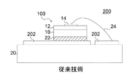
図1は、従来の発光部品又は光電部品の構造を示す図である。図1に示すとおり、従来の発光部品100は、透明基板10、この透明基板10上に位置する半導体積層12と、この半導体積層12上に位置する少なくとも一個の電極14とを含む。該半導体積層12は少なくとも、上から下へに向かって設けられた第一導電型半導体層120と、活性層122と、第二導電型半導体層124となどを含む。
FIG. 1 is a diagram showing the structure of a conventional light emitting component or photoelectric component. As shown in FIG. 1, a conventional
前記発光部品100とほかの部品とを組み合わせることにより、発光装置(Light Emitting apparatus)を更に形成することができる。図2は、従来の発光装置の構造を示す図である。図2に示すとおり、発光装置200は、サブ載置板(sab mount)20と、少なくとも1つの半田(solder)22と、電気接続構造24とを含む。該サブ載置板20は、少なくとも1つの電子回路202を具備する。前記半田22は、前記サブ載置板20上に位置する。この半田22で発光部品100をサブ載置板20上に接着固定させることにより、発光部品100の基板10とサブ載置板20上の電子回路202とを電気接続させる。前記電気接続構造24は、発光部品100の電極14とサブ載置板20上の電子回路202とを電気接続させる。前記サブ載置板20がリードフレーム(lead frame)又は大きいサイズのマウンティング基板(mounting substrate)であることにより、発光装置200の電子回路を容易に配置し、その放熱効果を向上させることができる。
By combining the
本発明の目的は、光電部品を提供することにある。 An object of the present invention is to provide a photoelectric component.
本発明の光電部品は、第一半導体層と、第二半導体層と、第二導電性電極と、少なくとも二個の第一導電性電極とを含む。第一半導体層は、少なくとも4つの辺縁と、第一表面と、第一表面の反対側にある第二表面とを具備し、かついずれか2つの隣接する辺縁により1つの隅部が形成される。第二半導体層は、第一半導体層の第一表面上に形成される。第二導電性電極は、第二半導体層上に形成される。第一導電性電極は、第一半導体層の第一表面上に形成され、かつ一部分の第一導電性電極が互いに離れていることにより設計状態を構成する。 The photoelectric component of the present invention includes a first semiconductor layer, a second semiconductor layer, a second conductive electrode, and at least two first conductive electrodes. The first semiconductor layer has at least four edges, a first surface, and a second surface opposite the first surface, and one corner is formed by any two adjacent edges. Is done. The second semiconductor layer is formed on a first surface of the first semiconductor layer. The second conductive electrode is formed on the second semiconductor layer. The first conductive electrode is formed on the first surface of the first semiconductor layer, and constitutes a design state by a part of the first conductive electrodes being separated from each other.
本発明は、光電部品又は発光部品及びその製造方法を公開する。本発明の説明をより詳細にするため、以下図3A〜図7に基づいて本発明を詳細に説明する。 The present invention discloses a photoelectric component or a light emitting component and a method for manufacturing the same. In order to make the description of the present invention more detailed, the present invention will be described in detail below with reference to FIGS.
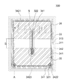
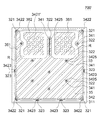
図3Aと図3Bは、本発明の第一実施例に係る光電部品300を示す平面図と断面図である。図3Bは、図3AのA−B−C方向に沿う断面を示す断面図である。光電部品300は1つの基板30を含む。この基板30は、単一な材料で構成される基板に限定されるものではなく、異なる複数の材料で構成される複合式基板であってもよい。例えば、基板30は、相互に接合される第一基板(図示せず)と第二基板(図示せず)とを含むことができる。
FIGS. 3A and 3B are a plan view and a cross-sectional view illustrating a
従来のエピタキシャル成長方法により、基板30上にエピタキシャル積層31を形成する。このエピタキシャル積層31は、第一表面3111とこの第一表面3111の反対側にある第二表面3112とを具備する第一半導体層311と、第一半導体層311の第一表面3111上に形成される活性層312と、この活性層312上に形成される第二半導体層313とを含む。次は、リソグラフィープロセス技術で一部分のエピタキシャル積層を削除することにより、光電部品300の辺縁の一部分の第一半導体層311を露出させるとともに、光電部品300中に溝渠Sを形成する。本実施例において、この溝渠Sは、一部分の第一半導体層311を露出させ、かつ第二半導体層313に囲まれている。平面図において、本実施例の溝渠Sは長い帯状に形成されている。
An
次は、化学気相成長方法(CVD)、物理気相成長方法(PVD)などの成長方法により、光電部品300のエピタキシャル積層31の表面と前記溝渠Sの側壁とに第一絶縁層341を形成する。
Next, the first
次は、光電部品300の辺縁付近に露出されている第一半導体層311上に、少なくとも一個の第一の第一導電性電極321を形成する。本実施例において、第一の第一導電性電極321は第二半導体層313に囲まれておらず、前記溝渠S中には第二の第一導電性電極322が形成されている。本実施例において、離れている第一の第一導電性電極321と第二の第一導電性電極322で第一導電性電極を形成する電極設計方法を採用する。
Next, at least one first first
本発明の実施例の電極設計方法は、電極の数量、電極の形状及び電極の位置を選択することにより、辺縁区域に接近する光電部品の電流分布を向上させることができる。例えば、この電極設計方法による第一導電性電極は、一個又は複数個の第一の第一導電性電極321と一個又は複数個の第二の第一導電性電極322と含み、上から見たこの第二の第一導電性電極322は、第二半導体層313に囲まれるとともに、長状に延伸されている。
In the electrode design method according to the embodiment of the present invention, the current distribution of the photoelectric component approaching the peripheral area can be improved by selecting the number of electrodes, the shape of the electrodes, and the positions of the electrodes. For example, the first conductive electrode according to this electrode design method includes one or a plurality of first
本実施例において、光電部品300の第一半導体層311は少なくとも4つの辺縁を含み、隣接する2つの辺縁は1つの隅部を形成し、かつ辺縁を乗り越える導電構造は存在しない。本実施例において、第一の第一導電性電極321は、光電部品300の同一辺縁の2つの隅部に形成され、かつ光電部品300の辺縁を乗り越えないように互いに離れている。
In this embodiment, the
本実施例において、第一半導体層311上に投影される第一の第一導電性電極321の投影は所定の形状を有する。この形状は、多辺形、円形、楕円形、半円形又は円弧面を有する形状であることができる。第二の第一導電性電極322は、線形、円弧形、線形と円弧形を組合せた形状、又はそれらの一部分を有する形状であることができる。本実施例において、第二の第一導電性電極322は先端と末端を有し、先端の幅は末端の幅より広い。
In this embodiment, the projection of the first first
次は、第二半導体層313上に第二導電性電極33を形成する。本実施例において、第一半導体層311上に投影された第二導電性電極33の投影面積と第二半導体層313の上表面面積の比は、90〜100%の間にある。
Next, the second
次は、前記第一の第一導電性電極321、第二の第一導電性電極322、第二導電性電極33及び一部分の第一絶縁層341の上に第二絶縁層342を形成する。第二絶縁層342は第一開口3421を具備することができ、この第一開口3421は、第二導電性電極33と後に続けて形成する第四電極36とを電気接続させることに用いられる。第二絶縁層342は第二開口3422を更に具備することができ、この第二開口3422は、第一の第一導電性電極321と後に続けて形成する第三電極35とを電気接続させることに用いられる。本実施例において、第一絶縁層341又は第二絶縁層342は、露出された前記第一半導体層311を完全に覆うことができる。
Next, a second insulating
本実施例において、前記第一絶縁層341又は第二絶縁層342は透明絶縁層であることができる。前記第一絶縁層341又は第二絶縁層342の材質は、酸化物、窒化物又はポリマー(polymer)であることができる。酸化物は、酸化アルミニウム(Al2O3)、二酸化ケイ素(SiO2)、酸化チタン(TiO2)、五酸化タンタル(Tantalun Pentoxide、Ta2O5)又は酸化アルミニウム(AlOx)を含み、窒化物は、窒化アルミニウム(AlN)、窒化ケイ素(SiNx)を含み、ポリマーは、ポリイミド(polyimide)、ベンゾシクロブテン(Benzocyclobutane、BCB)などのような材料又はこれらの組合せを含むことができる。本実施例において、第一絶縁層341又は第二絶縁層342は、分布ブラッグ反射器(Distributed Bragg Reflector)構造を有することができる。
In this embodiment, the first insulating
最後に、前記第二絶縁層342、第一の第一導電性電極321、第二の第一導電性電極322の上に第三電極35を形成するとともに、この第三電極35を第一の第一導電性電極321、第二の第一導電性電極322に電気接続させる。かつ、前記第二絶縁層342、第二導電性電極33上に第四電極36を形成するとともに、この第四電極36を第二導電性電極33に電気接続させる。本実施例の平面図において、第一半導体層311上に投影された第三電極35の投影面積と第四電極36の投影面積の比は、80〜100%の間にある。
Finally, a
本実施例において、第三電極35は一部分の第一の第一導電性電極321のみを覆うことができるが、他の実施例において、この第三電極35は第一の第一導電性電極321を覆わなくてもよい。
In the present embodiment, the
本実施例において、基板30の上表面から第三電極35の頂部までの高さはH1であり、基板30の上表面から第四電極36の頂部までの高さはH2であり、H1とH2は略同じである。本実施例において、H1とH2の差は5〜10%より小さい。H1とH2の差を調節することにより、光電部品300と後に続けて形成する載置板又は回路部品とによって形成されるフリップチップ構造の断線確率を低減し、製品の良品率を向上させることができる。本実施例において、第三電極35の辺縁と第四電極36の辺縁との間の最小距離はD1であり、D1は50μmより大きい。他の実施例において、D1は50〜200μm又は100〜200μmであることができる。
In this embodiment, the height from the upper surface of the
本実施例において、第一の第一導電性電極321、第二の第一導電性電極322、第二導電性電極33、第三電極35及び第四電極36は、多層構造であるとともに/或いは反射層(図示せず)を含むことができる。この反射層は、活性層312が発した光線を80%以上反射できる反射率を有する。本実施例において、第一の第一導電性電極321、第二の第一導電性電極322及び第三電極35は、1つのプロセスで形成することができる。本実施例において、活性層312が発した光線は、第一の第一導電性電極321、第二の第一導電性電極322、第二導電性電極33、第三電極35及び第四電極36に反射され、かつ基板30の方向から光電部品300の外部に出射される。
In this embodiment, the first first
所定の導電率を実現するため、第一の第一導電性電極321、第二の第一導電性電極322、第二導電性電極33、第三電極35及び第四電極36の材質が金属であることが好ましい。例えば、例えば、金(Au)、銀(Ag)、銅(Cu)、クロム(Cr)、アルミニウム(Al)、プラチナ(Pt)、ニッケル(Ni)、チタン(Ti)、スズ(Sn)などであるか、或いはそれらの合金又はそれらの積層構造であることができる。
In order to achieve a predetermined conductivity, the material of the first first
本実施例において、載置板又は回路部品(図示せず)を提供し、かつワイヤボンディング又は半田付けによりこの載置板又は回路部品上に第一載置板電極(図示せず)と第二載置板電極(図示せず)を形成することができる。この第一載置板電極及び第二載置板電極は、光電部品300の第三電極35及び第四電極36と共にフリップチップ構造を形成することができる。
In this embodiment, a mounting plate or a circuit component (not shown) is provided, and a first mounting plate electrode (not shown) and a second mounting plate electrode (not shown) are provided on the mounting plate or the circuit component by wire bonding or soldering. A mounting plate electrode (not shown) can be formed. The first mounting plate electrode and the second mounting plate electrode can form a flip chip structure together with the
本実施例において、第一の第一導電性電極321及び/又は第二の第一導電性電極322と第三電極35との間に第一調節層(図示せず)を形成するとともに、この第一調節層を第一の第一導電性電極321及び/又は第二の第一導電性電極322と第三電極35とに電気接続させることができる。他の実施例において、第二導電性電極33と第四電極36との間に第二調節層(図示せず)を形成するとともに、この第二調節層を第二導電性電極33と第四電極36とに電気接続させることができる。本実施例において、第一調節層と第二調節層はそれぞれ所定の高さを有し、かつ第一調節層と第二調節層の形成位置により、第一調節層と第二調節層の高さは前記高さH1とH2に影響を与えることができる(すなわち、高さH1とH2を調節することができる)。そのため、形成された第一調節層と第二調節層の高さをそれぞれ調節することにより、高さH1とH2との間の差を低減し、光電部品300と後に続けて形成する載置板又は回路部品とによって形成されるフリップチップ構造の断線確率を低減し、製品の良品率を向上させることができる。本実施例において、第一半導体層311上に投影された第一調節層の投影面積は、第一半導体層311上に投影された第三電極35の投影面積より大きいか、或いは第一半導体層311上に投影された第二調節層の投影面積は、第一半導体層311上に投影された第四電極36の投影面積より大きい。本実施例において、第一調節層又は第二調節層の材質が金属であることが好ましい。例えば、例えば、金(Au)、銀(Ag)、銅(Cu)、クロム(Cr)、アルミニウム(Al)、プラチナ(Pt)、ニッケル(Ni)、チタン(Ti)、スズ(Sn)などであるか、或いはそれらの合金又はそれらの積層構造であることができる。本実施例において、第一調節層又は第二調節層は、多層構造であるとともに/或いは反射層(図示せず)を含むことができる。この反射層は、活性層312が発した光線を80%以上反射できる反射率を有する。
In this embodiment, a first adjustment layer (not shown) is formed between the first first
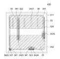
図3Cは、本発明の第二実施例に係る光電部品400を示す平面図である。本実施例の製造方法、使用する材料及び符号などは、上述した第一実施例のことと同一するので、ここでは再び説明しない。本発明の実施例の電極設計方法は、電極の数量、電極の形状及び電極の位置を選択することにより、辺縁区域に接近する光電部品400の電流分布を向上させることができる。
FIG. 3C is a plan view showing a
本実施例において、光電部品400の第一半導体層311は少なくとも4つの辺縁を含み、隣接する2つの辺縁は1つの隅部を形成し、かつ辺縁を乗り越える導電構造は存在しない。本実施例において、第一の第一導電性電極321は、第一半導体層311のいずれか1つの隅部上に形成される。第二絶縁層342は第二開口3422を具備することができ、この第二開口3422は、第一の第一導電性電極321と後に続けて形成する第三電極35とを電気接続させることに用いられる。第二の第一導電性電極322は、第一半導体層311上に形成され、かつ第二半導体層313に囲まれている。第二絶縁層342は第三開口3423を更に具備することができ、この第三開口3423は、第二の第一導電性電極322と後に続けて形成する第三電極35とを電気接続させることに用いられる。
In this embodiment, the
本実施例において、第一半導体層311上に投影される第一の第一導電性電極321の投影は所定の形状を有する。この形状は、多辺形、円形、楕円形、半円形又は円弧面を有する形状であることができる。第二の第一導電性電極322は延伸状に形成され、この形状は、線形、円弧形、線形と円弧形を組合せた形状、又はそれらの一部分を有する形状であることができる。本実施例において、第二の第一導電性電極322は先端と末端を有し、先端の幅は末端の幅より広い。
In this embodiment, the projection of the first first
本実施例において、光電部品400の辺縁付近に露出されている第一半導体層311上には、第三の第一導電性電極323が形成されている。本実施例において、第三の第一導電性電極323は第二半導体層313に囲まれていない。第二絶縁層342は第四開口3424を具備し、この第四開口3424は、第三の第一導電性電極323と後に続けて形成する第三電極35とを電気接続させることに用いられる。光電部品400の辺縁付近に露出されている第一半導体層311上には、第四の第一導電性電極324が形成されている。本実施例において、第四の第一導電性電極324は第二半導体層313に囲まれていない。第二絶縁層342は第五開口3425を具備し、この第五開口3425は、第四の第一導電性電極324と後に続けて形成する第三電極35とを電気接続させることに用いられる。
In the present embodiment, a third first
本実施例において、第一半導体層311上に投影される第三の第一導電性電極323の投影は所定の形状を有する。この形状は、多辺形、円形、楕円形、半円形又は円弧面を有する形状であることができる。第四の第一導電性電極324は、線形、円弧形、線形と円弧形を組合せた形状、又はそれらの一部分を有する形状であることができる。本実施例において、第四の第一導電性電極324は先端と末端を有し、先端の幅は末端の幅より広い。本実施例において、第三の第一導電性電極323と第四の第一導電性電極324の形状は相違している。
In this embodiment, the projection of the third first
本実施例において、製品の設計要求に応じて、第一の第一導電性電極321と第三の第一導電性電極323とを光電部品400の同一辺縁の付近に形成し、かつ両者を分離させることができる。本実施例において、第一の第一導電性電極321と第四の第一導電性電極324を、又は第三の第一導電性電極323と第四の第一導電性電極324を光電部品400の同一辺縁の付近に形成しなくてもよい。
In the present embodiment, the first first
本実施例において、第四の第一導電性電極324の先端は第三電極35に覆われており、第四の第一導電性電極324の末端は第四電極36に覆われていない。本実施例において、第一半導体層311上に投影された第三電極35の投影面積は、第一半導体層311上に投影された第四電極36の投影面積より大きく、かつ第一半導体層311上に投影された第三電極35の投影面積と第四電極36の投影面積の比は、110〜120%の間にある。本実施例において、第二の第一導電性電極322と第四の第一導電性電極324の末端の延伸方向は略平行している。
In this embodiment, the tip of the fourth first
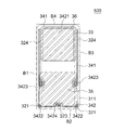
図4Aは、本発明の第三実施例に係る光電部品500を示す平面図である。本実施例の製造方法、使用する材料及び符号などは、上述した第一実施例のことと同一するので、ここでは再び説明しない。本発明の実施例の電極設計方法は、電極の数量、電極の形状及び電極の位置を選択することにより、辺縁区域に接近する光電部品500の電流分布を向上させることができる。
FIG. 4A is a plan view showing a
本実施例において、光電部品500の4つの辺縁は長方形を形成し、隣接する2つの辺縁は1つの隅部を形成し、かつ辺縁を乗り越える導電構造は存在しない。それらの辺縁は、第一長辺B1と、第二長辺B3と、第一短辺B2と、第二短辺B4とを含む。本実施例において、第一長辺B1又は第二長辺B3の長さは、第一短辺B2又は第二短辺B4の長さより長い。本実施例において、第一半導体層311上に投影された第三電極35と第四電極36の投影は、第一長辺B1又は第二長辺B3に沿って配列されている。
In this embodiment, the four edges of the
本実施例において、互いに離れている二個の第一の第一導電性電極321は、第一短辺B2の2つの隅部上に形成されている。第二絶縁層342は第二開口3422を具備することができ、この第二開口3422は、第一の第一導電性電極321と後に続けて形成する第三電極35とを電気接続させることに用いられる。二個の第四の第一導電性電極324はそれぞれ、第一短辺B2と第二短辺B4の辺縁付近に露出されている第一半導体層311上に形成されている。本実施例において、第三の第一導電性電極323は第一短辺B2上に形成されている。第二絶縁層342は第四開口3424を具備し、この第四開口3424は、第三の第一導電性電極323と後に続けて形成する第三電極35とを電気接続させることに用いられる。第四の第一導電性電極324は第二半導体層313に囲まれていない。第二絶縁層342は第三開口3423を具備することができ、この第三開口3423は、第四の第一導電性電極324と後に続けて形成する第三電極35とを電気接続させることに用いられる。
In the present embodiment, two first first
本実施例において、第三の第一導電性電極323から前記二個の第一の第一導電性電極321までの距離は略同じである。第一の第一導電性電極321、第四の第一導電性電極324及び第三電極35は、1つのプロセスで形成することができる。
In this embodiment, the distance from the third first
本実施例において、第一半導体層311上に投影される第一の第一導電性電極321の投影は所定の形状を有する。この形状は、多辺形、円形、楕円形、半円形又は円弧面を有する形状であることができる。第一半導体層311上に投影される第三の第一導電性電極323の投影は所定の形状を有し、この形状は、多辺形、円形、楕円形、半円形又は円弧面を有する形状であることができる。第四の第一導電性電極324は延伸状に形成され、この形状は、線形、円弧形、線形と円弧形を組合せた形状、又はそれらの一部分を有する形状であることができる。本実施例において、第四の第一導電性電極324は先端と末端を有し、この先端の幅は末端の幅より広い。本実施例において、第三の第一導電性電極323と第四の第一導電性電極324の形状は相違している。
In this embodiment, the projection of the first first
本実施例において、前記第四の第一導電性電極324の先端は第一短辺B2に向かい、末端は第二短辺B4に向かう。本実施例において、第四の第一導電性電極324の先端は第三電極35に覆われており、第四の第一導電性電極324の末端は第四電極36に覆われていない。本実施例において、前記二個の第四の第一導電性電極324の末端の延伸方向は略平行している。本実施例において、第一半導体層311上に投影された第三電極35の投影面積は、第一半導体層311上に投影された第四電極36の投影面積より大きく、かつ第一半導体層311上に投影された第三電極35の投影面積と第四電極36の投影面積の比は、110〜120%の間にある。
In the present embodiment, the tip of the fourth first
図4Bは、本発明の第四実施例に係る光電部品600を示す平面図である。本実施例の製造方法、使用する材料及び符号などは、上述した第一実施例のことと同一するので、ここでは再び説明しない。本発明の実施例の電極設計方法は、電極の数量、電極の形状及び電極の位置を選択することにより、辺縁区域に接近する光電部品600の電流分布を向上させることができる。
FIG. 4B is a plan view showing a
本実施例において、光電部品600の4つの辺縁は長方形を形成し、隣接する2つの辺縁は1つの隅部を形成し、かつ辺縁を乗り越える導電構造は存在しない。光電部品600は、第一長辺B1と、第二長辺B3と、第一短辺B2と、第二短辺B4とを含む。本実施例において、第一長辺B1又は第二長辺B3の長さは、第一短辺B2又は第二短辺B4の長さより長い。本実施例において、第一半導体層311上に投影された第三電極35と第四電極36の投影は、第一長辺B1又は第二長辺B3に沿って配列されている。
In the present embodiment, the four edges of the
本実施例は、少なくとも一個の第一の第一導電性電極321を含む。本実施例において、四個の第一の第一導電性電極321を第一半導体層311の4つの隅部上に形成することができる。第二絶縁層342は第二開口3422を更に具備することができ、この第二開口3422は、第一の第一導電性電極321と後に続けて形成する第三電極35とを電気接続させることに用いられる。二個の第二の第一導電性電極322は、第一半導体層311上に形成され、かつ第二半導体層313に囲まれている。第二絶縁層342は第三開口3423を更に具備することができ、この第三開口3423は、第二の第一導電性電極322と後に続けて形成する第三電極35とを電気接続させることに用いられる。
This embodiment includes at least one first first
本実施例において、第一半導体層311上に投影される第一の第一導電性電極321の投影は所定の形状を有する。この形状は、多辺形、円形、楕円形、半円形又は円弧面を有する形状であることができる。第一半導体層311上に投影される第二の第一導電性電極322の投影は所定の形状を有し、この形状は、多辺形、円形、楕円形、半円形又は円弧面を有する形状であることができる。第四の第一導電性電極324は延伸状に形成され、この形状は、線形、円弧形、線形と円弧形を組合せた形状、又はそれらの一部分を有する形状であることができる。本実施例において、第一半導体層311上に投影された前記二個の第二の第一導電性電極322の投影の形状は、同一又は相違している。
In this embodiment, the projection of the first first
本実施例において、第三電極35は2つの延伸部351を含み、かつこの2つの延伸部351により略凹部Rが形成される。第四電極36はその凹部R内に位置する。第一の第一導電性電極321、第二の第一導電性電極322及び第三電極35は、1つのプロセスで形成することができる。
In the present embodiment, the
図4Cは、本発明の第五実施例に係る光電部品700を示す平面図である。本実施例の製造方法、使用する材料及び符号などは、上述した第一実施例のことと同一するので、ここでは再び説明しない。本発明の実施例の電極設計方法は、電極の数量、電極の形状及び電極の位置を選択することにより、辺縁区域に接近する光電部品700の電流分布を向上させることができる。
FIG. 4C is a plan view showing the
本実施例において、光電部品700の第一半導体層311は少なくとも4つの辺縁を含み、隣接する2つの辺縁は1つの隅部を形成し、かつ辺縁を乗り越える導電構造は存在しない。本実施例は、第一半導体層311の4つの隅部上にそれぞれ形成される四個の第一の第一導電性電極321を含む。第二絶縁層342は第二開口3422を具備することができ、この第二開口3422は、第一の第一導電性電極321と後に続けて形成する第三電極35とを電気接続させることに用いられる。第一半導体層311上に形成されている複数個の第二の第一導電性電極322は、第二半導体層313に囲まれている。第二絶縁層342は第四開口3424を具備し、この第四開口3424は、第二の第一導電性電極322と後に続けて形成する第三電極35とを電気接続させることに用いられる。光電部品700の辺縁付近に露出されている第一半導体層311上には、複数個の第三の第一導電性電極323が形成されている。すなわち、第三の第一導電性電極323は第二半導体層313に囲まれず、第一半導体層311のいずれか1つの辺縁は一個又は複数個の第三の第一導電性電極323を含むことができる。第二絶縁層342は第三開口3423を更に具備することができ、この第三開口3423は、第二の第一導電性電極322と後に続けて形成する第三電極35とを電気接続させることに用いられる。
In this embodiment, the
本実施例において、第一半導体層311上に投影される第一の第一導電性電極321の投影は所定の形状を有する。この形状は、多辺形、円形、楕円形、半円形又は円弧面を有する形状であることができる。第一半導体層311上に投影される第二の第一導電性電極322の投影は所定の形状を有し、この形状は、多辺形、円形、楕円形、半円形又は円弧面を有する形状であることができる。本実施例において、第二の第一導電性電極322は延伸状に形成され、かつこの延伸方向は延伸部351の延伸方向に平行する。第二の第一導電性電極322の形状は、線形、円弧形、線形と円弧形を組合せた形状、又はそれらの一部分を有する形状であることができる。本実施例において、第一半導体層311上に投影された前記複数個の第二の第一導電性電極322の投影の形状は、同一又は相違している。第一半導体層311上に投影された第三の第一導電性電極323の投影は所定の形状を有し、この形状は、多辺形、円形、楕円形、半円形又は円弧面を有する形状であることができる。
In this embodiment, the projection of the first first
本実施例において、第三電極35は3つの延伸部351を含み、かつこの3つの延伸部351により2つの略凹部Rが形成される。2個の第四電極36をその凹部R内に形成することができる。本実施例において、少なくとも1個の第二の第一導電性電極322はその凹部R内に形成することができる。
In this embodiment, the
本実施例において、第一半導体層311上に投影された前記第一の第一導電性電極321、第二の第一導電性電極322、第三の第一導電性電極323及び第三電極35の投影の形状は、同一又は相違することができる。かつ第一の第一導電性電極321、第二の第一導電性電極322、第三の第一導電性電極323及び第三電極35は、1つのプロセスで形成することができる。
In this embodiment, the first first
図4Dは、本発明の第六実施例に係る光電部品700`を示す平面図である。本実施例は、第五実施例の変形例であり、その製造方法、使用する材料及び符号などは、上述した第五実施例のことと同一するので、ここでは再び説明しない。
FIG. 4D is a plan view showing a
本実施例において、光電部品700`の第二絶縁層342は、複数の第一開口3421`を具備し、これらの第一開口は、第二導電性電極33と後に続けて形成する第四電極36とを電気接続させることに用いられる。本実施例において、第二絶縁層342が複数の第一開口3421`を具備することにより、第三電極35と第四電極36の高さの差を低減し、かつ後に続けて形成する載置板又は回路部品とによって形成されるフリップチップ構造の断線確率を低減することにより、製品の良品率を向上させることができる。
In this embodiment, the second insulating
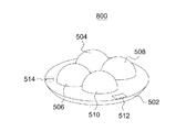
図5A〜図5Cは発光モジュールを示す図であり、図5Aは発光モジュールの外部を示す斜視図である。この発光モジュール800は、載置体502と、光電部品(図示せず)と、複数個のレンズ504、506、508及び510と、二個の電力供給端末512及び514とを含む。その発光モジュール800は、後述する発光ユニット540に連結される。
5A to 5C are views showing a light emitting module, and FIG. 5A is a perspective view showing the outside of the light emitting module. The
図5B〜図5Cは、発光モジュール800の断面を示す図であり、図5Cは、図5BのE区域を示す拡大図である。載置体502は上載置体503と下載置体501を含み、下載置体501の一表面は上載置体503に接触する。レンズ504及び508は上載置体503に形成される。上載置体503には、少なくとも一つの孔515が形成されており、本発明の実施例の光電部品300又はほかの実施例の光電部品(図示せず)は、下載置体501と接触するように該孔515に設けられ、かつ接着剤521に覆われる。接着剤521上にはレンズ508が設けられ、接着剤521の材料はシリコン樹脂、エポキシ樹脂又はほかの材料である。この実施例において、孔515の両側の側壁に反射層519を形成することにより、光取り出し効率を増加させ、かつ下載置体501の下表面に金属層517を形成することにより、放熱効果を向上させることができる。
5B to 5C are views showing a cross section of the
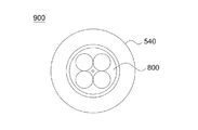
図6A〜図6Bは、光線生成装置900を示す図である。この光線生成装置900は、発光モジュールと800と、発光ユニット540と、発光モジュールと800に所定の電流を提供する電源供給システム(図示せず)と、電源供給システム(図示せず)を制御する制御部品(図示せず)とを含む。光線生成装置900は、照明装置であることができる。例えば、街路燈、車燈又は室内照明装置であるか、或いは交通信号標識又は平面表示装置のバックライトモジュールのバックライトである。
6A and 6B are views showing the light
図7は電球を示す図である。電球1000は、カバー921と、レンズ922と、照明モジュール924と、フレーム925と、放熱器926と、挿入部927と、金口928とを含む。該照明モジュール924は、載置体923と、載置体923上に載置される本発明の実施例の少なくとも一個の光電部品300又はほかの実施例の光電部品(図示せず)とを含む。
FIG. 7 is a view showing a light bulb. The
具体的に、基板30は成長(例えば、エピタキシャルの成長)及び/又は載置の基礎になる。基板の種類として、導電基板、不導電基板、透明基板又は不透明基板を選択することができる。導電基板の材料は、ゲルマニウム(Ge)、ヒ化ガリウム(GaAs)、リン化インジウム(InP)、炭化ケイ素(SiC)、ケイ素(Si)、アルミン酸リチウム(LiAlO2)、酸化亜鉛(ZnO)、窒化ガリウム(GaN)、窒化アルミニウム(AlN)、金属であることができる。透明基板の材料は、サファイア(Sapphire)、アルミン酸リチウム(LiAlO2)、酸化亜鉛(ZnO)、窒化ガリウム(GaN)、ガラス、ダイヤモンド、CVDダイヤモンド、ダイヤモンド状カーボン(Diamond−Like Carbon、DLC)、スピネル(spinel、MgAl2O4)、酸化アルミニウム(Al2O3)、酸化ケイ素(SiOx)、リチウムガレート(LiGaO2)であることができる。
Specifically,
エピタキシャル積層31は、第一半導体層311と、活性層312と、第二半導体層313とを含む。第一半導体層311と第二半導体層313は、例えばクラッド層(cladding layer)又は制限層(confinement layer)になり、かつ単層構造又は多層構造に形成されることができる。前記第一半導体層311と第二半導体層313の種類、極性又は不純物は相違している。半導体層の種類として、p型、n型、i型のうちいずれか2種の組合せを選択することができる。半導体層は電子と正孔(Electron hole)をそれぞれ提供し、この電子と正孔が活性層312で反応して発光するようにする。第一半導体層311、活性層312及び第二半導体層313の材料は、III−V族半導体材料を含むことができる。例えば、AlxInyGa(1−x−y)N又はAlxInyGa(1−x−y)Pを含むことができ、この化学式において、0≦x、y≦1、(x+y)≦1である。活性層312の材料によってエピタキシャル積層は、波長の範囲が610nm〜650nmの間にある赤光、波長の範囲が530nm〜570nmの間にある緑光、波長の範囲が450nm〜490nmの間にある青光、又は波長が400nmより小さい赤外線を発することができる。
The
本発明の他の実施例において、光電部品300、400、500、600、700、700`は、エピタキシャル部品又は発光ダイオードであり、この発光光線の周波数スペクトルは、エピタキシャル積層において単層又は多層のような物理的要素又は化学的要素を変更することにより調節することができる。単層又は多層のエピタキシャル積層の材料は、アルミニウム(Al)、ガリウム(Ga)、インジウム(In)、リン(P)、窒素(N)、亜鉛(Zn)、酸素(O)で構成された組から選択されることができる。活性層312の構造は、例えば、シングルヘテロ構造(single heterostructure、SH)、ダブルヘテロ構造(double heterostructure、DH)、両側ダブルヘテロ構造(double−side double heterostructure、DDH)、又は多層量子井戸構造(multi−quantun well、MQW)である。また、活性層312の量子井戸の対数を調節することによっても発光光線の波長を変更することができる。
In another embodiment of the present invention, the
本発明の実施例において、必要に応じて第一半導体層311と基板30との間に緩衝層(buffer layer、図示せず)を形成することができる。この緩衝層を二種の材料の間の設けることにより、基板30の材料システムから第一半導体層311の材料システムへの過渡を実現することができる。発光ダイオードの構造において、緩衝層は、二種の材料の間の結晶格子が合わないことを低減する材料層になることができる。また、この緩衝層により、二種の材料、又は離れている二個の単層、多層又は構造を貼り合せることができる。緩衝層の材料は、例えば有機材料、無機材料、金属、半導体などから選択されることができる。緩衝層の構造は、反射層、導熱層、導電層、オーミック接触(ohmic contact)層、変形防止層、応力除去(stress release)層、応力調節(stress adjustment)層、ボンディング(bonding)層、波長変更層、機械的固定構造などになることができる。この実施例において、その緩衝層の材料は、窒化アルミニウム又は窒化ガリウムから選択され、かつスパッタリング又は原子層堆積装置(Atomic Layer Deposition、ALD)の方法でその緩衝層を形成することができる。
In the embodiment of the present invention, a buffer layer (not shown) may be formed between the
第二半導体層313と第二導電性電極33との間には、接触層(図示せず)を更に形成することができる。具体的に、この接触層は、光学層、電気層、又はそれらの組合せであることができる。光学層は、活性層から来るか或いは活性層に入射される電磁波又は光線を変更することができる。この「変更」とは、電磁波又は光線の少なくとも一種の光学特性を変更することをいう。この光学特性は、周波数、波長、強度、通量、効率、色温度、演色性(rendering index)、ライトフィールド(light field)、画角(angle of view)などを含むが、これらに限定されるものではない。電気層は、接触層のいずれか一組とその対向側との間の電圧、抵抗、電流、電気容量のうち少なくとも1つの数値、密度、分布が変化するようにするか或いは変化の趨勢が出るようにする。接触層の構成材料は、酸化物、導電酸化物、透明酸化物、50%以上の透明率を有する酸化物、金属、透光金属、50%又はその以上の透過率を有する金属、有機物、無機物、蛍光物、リン光物、セラミックス、半導体、不純物を含有する半導体、不純物を含有しない半導体のうちの少なくとも一種を含むことができる。ある応用おいて、接触層の材料は、酸化インジウムスズ、酸化スズカドミウム、酸化スズアンチモン、酸化インジウム亜鉛、酸化亜鉛アルミニウム、酸化亜鉛スズのうちの少なくとも一種であることができる。透光型金属を採用する場合、その厚さが0.005〜0.6μmであることが好ましい。
A contact layer (not shown) may be further formed between the
以上、これらの発明の実施例を図面により詳述してきたが、実施例はこの発明の例示にしか過ぎないものであるため、この発明は実施例の構成にのみ限定されるものではなく、この発明の要旨を逸脱しない範囲の設計の変更等があってもこの発明に含まれることは勿論である。また、例えば、各実施例に複数の構成が含まれている場合には、特に記載がなくとも、これらの構成の可能な組合せが含まれることは勿論である。また、複数の実施例や変形例が示されている場合には、特に記載がなくとも、これらに跨がった構成の組合せのうちの可能なものが含まれることは勿論である。また、図面に描かれている構成については、特に記載がなくとも、含まれることは勿論である。更に、「等」の用語がある場合には、同等のものを含むという意味で用いられている。また、「ほぼ」「約」「程度」などの用語がある場合には、常識的に認められる範囲や精度のものを含むという意味で用いられている。 As described above, the embodiments of the present invention have been described in detail with reference to the drawings. However, since the embodiments are merely examples of the present invention, the present invention is not limited only to the configurations of the embodiments. Of course, even if there is a change in the design within a range not departing from the gist of the invention, it is included in the present invention. Further, for example, when a plurality of configurations are included in each embodiment, it goes without saying that possible combinations of these configurations are included even if not specifically described. Further, in the case where a plurality of embodiments and modified examples are shown, it is needless to say that possible combinations of configurations that straddle these are included, even if not particularly described. Further, it is needless to say that the configuration depicted in the drawings is included even if not particularly described. Further, when there is a term such as “etc.”, it is used to mean that it includes the equivalent. Further, when there is a term such as “substantially”, “about”, or “degree”, it is used in a sense that the term includes a range and accuracy recognized by common sense.
300、400、500、600、700、700` 光電部品
30 基板
31 エピタキシャル積層
311 第一半導体層
3111 第一表面
3112 第二表面
312 活性層
313 第二半導体層
S 溝渠
341 第一絶縁層
342 第二絶縁層
3421、3421` 第一開口
3422 第二開口
3423 第三開口
3424 第四開口
3425 第五開口
321 第一の第一導電性電極
322 第二の第一導電性電極
323 第三の第一導電性電極
324 第四の第一導電性電極
33 第二導電性電極
35 第三電極
B1 第一長辺
B3 第二長辺
B2 第一短辺
B4 第二短辺
351 延伸部
R 凹部
36 第四電極
800 発光モジュール
501 下載置体
502 載置体
503 上載置体
504、506、508、510 レンズ
512、514 電力供給端末
515 孔
517 金属層
519 反射層
521 接着剤
540 発光ユニット
900 光線生成装置
1000 電球
921 カバー
922 レンズ
923 載置体
924 照明モジュール
925 フレーム
926 放熱器
927 挿入部
928 金口
H1、H2 高さ
D1 最小距離
300, 400, 500, 600, 700, 700`
Claims (10)
2つの長辺と2つの短辺を有し、かついずれかの前記長辺と前記短辺により隅部が形成される第一半導体層と、
前記第一半導体層上に形成される第二半導体層と、
前記第二半導体層上に形成される第二導電性電極と、
前記第一半導体層の前記隅部に形成され、かつ前記第一半導体層上に投影される投影が所定の形状を有し、前記形状が多辺形、円形、楕円形、半円形を含む第一導電性電極と、
前記第一半導体層の前記2つの前記長辺の一つに接近し、かつ先端と末端を有し、前記先端の幅が前記末端の幅より広いもう一つの第一導電性電極と、
前記第二半導体層、前記第一導電性電極及び前記もう一つの第一導電性電極を覆う第三電極と、
前記第二半導体層及び前記第二導電性電極を覆う第四電極とを含み、
前記第一導電性電極と前記もう一つの第一導電性電極が分離し、互いに接触しない光電部品。 Photoelectric components,
A first semiconductor layer having two long sides and two short sides, and a corner formed by one of the long sides and the short sides;
A second semiconductor layer formed on the first semiconductor layer,
A second conductive electrode formed on the second semiconductor layer,
The projection formed on the corner of the first semiconductor layer and projected on the first semiconductor layer has a predetermined shape, and the shape includes a polygon, a circle, an ellipse, and a semicircle. One conductive electrode;
And wherein the first semiconductor layer close to one of the two said long sides, and having a distal end and a distal, the tip first conductive electrode width is wider another than the width of the end of,
A third electrode covering the second semiconductor layer, the first conductive electrode and the another first conductive electrode,
Including a fourth electrode covering the second semiconductor layer and the second conductive electrode,
The photoelectric component, wherein the first conductive electrode and the another first conductive electrode are separated from each other and do not contact each other.
前記接触層は酸化物、導電酸化物、又は透明酸化物を含む、請求項1に記載の光電部品。 Further comprising a contact layer located between the second semiconductor layer and the second conductive electrode,
The photoelectric component according to claim 1, wherein the contact layer includes an oxide, a conductive oxide, or a transparent oxide.
前記第三電極及び前記第四電極はそれぞれ、前記第二半導体層上に位置する辺縁を含み、かつ、前記第三電極の前記辺縁と前記第四電極の前記辺縁との間に50〜200μmの最小距離を有する、請求項1に記載の光電部品。 The projected area of the third electrode projected on the first semiconductor layer is larger than the projected area of the fourth electrode projected on the first semiconductor layer,
The third electrode and the fourth electrode each include an edge located on the second semiconductor layer, and a distance between the edge of the third electrode and the edge of the fourth electrode is 50. The photoelectric component according to claim 1, having a minimum distance of 200 μm.
前記第一開口は前記第二導電性電極と第四電極とを電気接続させることに用いられ、
前記第二開口は前記第一導電性電極と第三電極とを電気接続させることに用いられ、又は前記もう一つの第一導電性電極と前記第三電極とを電気接続させることに用いれ、
前記絶縁層は、分布ブラッグ反射器(Distributed Bragg Reflector)構造を有する、請求項2に記載の光電部品。 Further comprising an insulating layer having a first opening and a second opening,
The first opening is used to electrically connect the second conductive electrode and a fourth electrode,
The second opening is used to electrically connect the first conductive electrode and the third electrode, or used to electrically connect the another first conductive electrode and the third electrode,
The photoelectric component according to claim 2, wherein the insulating layer has a distributed Bragg reflector structure.
第一半導体層と、
前記第一半導体層上に形成される第二半導体層と、
前記第一半導体層を露出させ、かつ前記第二半導体層に囲まれている溝渠と、
前記溝渠中に形成される第一導電性電極と、
前記第一半導体層上に形成され、かつ前記第一導電性電極と分離しているもう一つの第一導電性電極と、
前記第二半導体層上に形成される第二導電性電極と、
前記溝渠の側壁上に形成される第一絶縁層と、
前記第一導電性電極、前記もう一つの第一導電性電極、前記第二導電性電極及び前記第一絶縁層上に形成される第二絶縁層と、
前記第二絶縁層上に形成され、かつ前記第一導電性電極を覆わない第三電極と、
前記第二絶縁層と前記第二導電性電極上に形成される第四電極と、
前記第一導電性電極、前記もう一つの第一導電性電極及び前記第三電極との間に形成され、かつ前記第一導電性電極及び前記第三電極に電気的に接続される第一調節層と、
前記第二導電性電極と前記第四電極との間に形成され、かつ前記第二導電性電極及び前記第四電極に電気的に接続される第二調節層とを含む、光電部品。 Photoelectric components,
A first semiconductor layer;
A second semiconductor layer formed on the first semiconductor layer,
A ditch that exposes the first semiconductor layer and is surrounded by the second semiconductor layer,
A first conductive electrode formed in the trench,
Another first conductive electrode formed on the first semiconductor layer and separated from the first conductive electrode,
A second conductive electrode formed on the second semiconductor layer,
A first insulating layer formed on a side wall of the trench,
The first conductive electrode, the another first conductive electrode, a second insulating layer formed on the second conductive electrode and the first insulating layer,
A third electrode formed on the second insulating layer and not covering the first conductive electrode,
A fourth electrode formed on the second insulating layer and the second conductive electrode,
A first adjustment formed between the first conductive electrode , the another first conductive electrode and the third electrode, and electrically connected to the first conductive electrode and the third electrode; Layers and
An optoelectronic component, comprising: a second adjustment layer formed between the second conductive electrode and the fourth electrode and electrically connected to the second conductive electrode and the fourth electrode.
第一半導体層と、
前記第一半導体層上に形成される第二半導体層と、
前記第一半導体層を露出させ、かつ前記第二半導体層に囲まれている溝渠と、
前記溝渠中に形成される第一導電性電極と、
前記第一半導体層上に形成され、かつ前記第一導電性電極と分離しているもう一つの第一導電性電極と、
前記第二半導体層上に形成される第二導電性電極と、
前記溝渠の側壁上に形成される第一絶縁層と、
前記第一導電性電極、前記もう一つの第一導電性電極、前記第二導電性電極及び前記第一絶縁層上に形成される第二絶縁層と、
前記第二絶縁層上に形成され、かつ前記第一導電性電極を覆う第三電極と、
前記第二絶縁層と前記第二導電性電極上に形成される第四電極と、
前記第一導電性電極、前記もう一つの第一導電性電極及び前記第三電極との間に形成され、かつ前記第一導電性電極と前記第三電極に電気接続される第一調節層と、
前記第二導電性電極と前記第四電極との間に形成され、かつ前記第二導電性電極と前記第四電極に電気接続される第二調節層とを含み、
前記第一半導体層上に投影された前記第一調節層の投影面積は、前記第一半導体層上に投影された前記第三電極の投影面積より大きい、光電部品。 Photoelectric components,
A first semiconductor layer;
A second semiconductor layer formed on the first semiconductor layer,
A ditch that exposes the first semiconductor layer and is surrounded by the second semiconductor layer,
A first conductive electrode formed in the trench,
Another first conductive electrode formed on the first semiconductor layer and separated from the first conductive electrode,
A second conductive electrode formed on the second semiconductor layer,
A first insulating layer formed on a side wall of the trench,
The first conductive electrode, the another first conductive electrode, a second insulating layer formed on the second conductive electrode and the first insulating layer,
A third electrode formed on the second insulating layer and covering the first conductive electrode,
A fourth electrode formed on the second insulating layer and the second conductive electrode,
A first adjustment layer formed between the first conductive electrode , the another first conductive electrode and the third electrode, and electrically connected to the first conductive electrode and the third electrode; ,
A second adjustment layer formed between the second conductive electrode and the fourth electrode, and electrically connected to the second conductive electrode and the fourth electrode,
The photoelectric component, wherein a projected area of the first adjustment layer projected on the first semiconductor layer is larger than a projected area of the third electrode projected on the first semiconductor layer.
Priority Applications (2)
| Application Number | Priority Date | Filing Date | Title |
|---|---|---|---|
| JP2014153402A JP6636237B2 (en) | 2014-07-29 | 2014-07-29 | Photoelectric components |
| JP2019228240A JP6942780B2 (en) | 2014-07-29 | 2019-12-18 | Photoelectric parts |
Applications Claiming Priority (1)
| Application Number | Priority Date | Filing Date | Title |
|---|---|---|---|
| JP2014153402A JP6636237B2 (en) | 2014-07-29 | 2014-07-29 | Photoelectric components |
Related Child Applications (1)
| Application Number | Title | Priority Date | Filing Date |
|---|---|---|---|
| JP2019228240A Division JP6942780B2 (en) | 2014-07-29 | 2019-12-18 | Photoelectric parts |
Publications (3)
| Publication Number | Publication Date |
|---|---|
| JP2016032009A JP2016032009A (en) | 2016-03-07 |
| JP2016032009A5 JP2016032009A5 (en) | 2017-08-31 |
| JP6636237B2 true JP6636237B2 (en) | 2020-01-29 |
Family
ID=55442227
Family Applications (1)
| Application Number | Title | Priority Date | Filing Date |
|---|---|---|---|
| JP2014153402A Active JP6636237B2 (en) | 2014-07-29 | 2014-07-29 | Photoelectric components |
Country Status (1)
| Country | Link |
|---|---|
| JP (1) | JP6636237B2 (en) |
Families Citing this family (4)
| Publication number | Priority date | Publication date | Assignee | Title |
|---|---|---|---|---|
| TWI790984B (en) * | 2017-01-26 | 2023-01-21 | 晶元光電股份有限公司 | Light-emitting device |
| EP3528296B1 (en) | 2018-02-16 | 2020-06-03 | Nichia Corporation | Light emitting element and light emitting device |
| JP6912731B2 (en) | 2018-07-31 | 2021-08-04 | 日亜化学工業株式会社 | Semiconductor light emitting device |
| DE102018122568A1 (en) * | 2018-09-14 | 2020-03-19 | Osram Opto Semiconductors Gmbh | OPTOELECTRONIC SEMICONDUCTOR COMPONENT WITH FIRST AND SECOND CONTACT ELEMENTS AND METHOD FOR PRODUCING THE OPTOELECTRONIC SEMICONDUCTOR COMPONENT |
Family Cites Families (4)
| Publication number | Priority date | Publication date | Assignee | Title |
|---|---|---|---|---|
| JP4882792B2 (en) * | 2007-02-25 | 2012-02-22 | 日亜化学工業株式会社 | Semiconductor light emitting device |
| JP5989420B2 (en) * | 2012-06-28 | 2016-09-07 | 株式会社東芝 | Semiconductor light emitting device |
| JP5929714B2 (en) * | 2012-11-07 | 2016-06-08 | 日亜化学工業株式会社 | Semiconductor light emitting device |
| TWI570955B (en) * | 2013-01-10 | 2017-02-11 | 晶元光電股份有限公司 | Light-emitting device |
-
2014
- 2014-07-29 JP JP2014153402A patent/JP6636237B2/en active Active
Also Published As
| Publication number | Publication date |
|---|---|
| JP2016032009A (en) | 2016-03-07 |
Similar Documents
| Publication | Publication Date | Title |
|---|---|---|
| US11908975B2 (en) | Optoelectronic device and method for manufacturing the same | |
| JP6529223B2 (en) | Photoelectric parts | |
| JP6636237B2 (en) | Photoelectric components | |
| JP6843916B2 (en) | Photoelectric parts | |
| JP6942780B2 (en) | Photoelectric parts | |
| JP7118227B2 (en) | photoelectric components | |
| KR102331621B1 (en) | Optoelectronic device | |
| JP7223046B2 (en) | photoelectric components | |
| KR102146966B1 (en) | Optoelectronic device | |
| KR102394347B1 (en) | Optoelectronic device | |
| KR102059974B1 (en) | Optoelectronic device | |
| KR102198133B1 (en) | Optoelectronic device | |
| CN105322066B (en) | Photoelectric element and manufacturing method thereof | |
| KR101974976B1 (en) | Optoelectronic device and method for manufacturing the same | |
| TWI790911B (en) | Optoelectronic device | |
| TWI790912B (en) | Optoelectronic device | |
| TWI758603B (en) | Optoelectronic device and method for manufacturing the same | |
| TWI662720B (en) | Optoelectronic device and method for manufacturing the same | |
| KR20160002063A (en) | Optoelectronic device and method for manufacturing the same | |
| TW202327127A (en) | Optoelectronic device |
Legal Events
| Date | Code | Title | Description |
|---|---|---|---|
| A521 | Request for written amendment filed |
Free format text: JAPANESE INTERMEDIATE CODE: A523 Effective date: 20170721 |
|
| A621 | Written request for application examination |
Free format text: JAPANESE INTERMEDIATE CODE: A621 Effective date: 20170721 |
|
| A977 | Report on retrieval |
Free format text: JAPANESE INTERMEDIATE CODE: A971007 Effective date: 20180523 |
|
| A131 | Notification of reasons for refusal |
Free format text: JAPANESE INTERMEDIATE CODE: A131 Effective date: 20180703 |
|
| A521 | Request for written amendment filed |
Free format text: JAPANESE INTERMEDIATE CODE: A523 Effective date: 20181002 |
|
| A131 | Notification of reasons for refusal |
Free format text: JAPANESE INTERMEDIATE CODE: A131 Effective date: 20190319 |
|
| A521 | Request for written amendment filed |
Free format text: JAPANESE INTERMEDIATE CODE: A523 Effective date: 20190613 |
|
| TRDD | Decision of grant or rejection written | ||
| A01 | Written decision to grant a patent or to grant a registration (utility model) |
Free format text: JAPANESE INTERMEDIATE CODE: A01 Effective date: 20191119 |
|
| A61 | First payment of annual fees (during grant procedure) |
Free format text: JAPANESE INTERMEDIATE CODE: A61 Effective date: 20191218 |
|
| R150 | Certificate of patent or registration of utility model |
Ref document number: 6636237 Country of ref document: JP Free format text: JAPANESE INTERMEDIATE CODE: R150 |
|
| R250 | Receipt of annual fees |
Free format text: JAPANESE INTERMEDIATE CODE: R250 |
|
| R250 | Receipt of annual fees |
Free format text: JAPANESE INTERMEDIATE CODE: R250 |