RU2462786C2 - Method and apparatus for epitaxial growth of type iii-v semiconductors, apparatus for generating low-temperature high-density plasma, epitaxial metal nitride layer, epitaxial metal nitride heterostructure and semiconductor - Google Patents
Method and apparatus for epitaxial growth of type iii-v semiconductors, apparatus for generating low-temperature high-density plasma, epitaxial metal nitride layer, epitaxial metal nitride heterostructure and semiconductor Download PDFInfo
- Publication number
- RU2462786C2 RU2462786C2 RU2007135977/28A RU2007135977A RU2462786C2 RU 2462786 C2 RU2462786 C2 RU 2462786C2 RU 2007135977/28 A RU2007135977/28 A RU 2007135977/28A RU 2007135977 A RU2007135977 A RU 2007135977A RU 2462786 C2 RU2462786 C2 RU 2462786C2
- Authority
- RU
- Russia
- Prior art keywords
- plasma
- vacuum chamber
- epitaxial
- semiconductor
- metal
- Prior art date
Links
- 229910052751 metal Inorganic materials 0.000 title claims abstract description 64
- 239000002184 metal Substances 0.000 title claims abstract description 63
- 239000004065 semiconductor Substances 0.000 title claims abstract description 49
- 230000012010 growth Effects 0.000 title claims abstract description 45
- 238000000034 method Methods 0.000 title claims description 87
- 150000004767 nitrides Chemical class 0.000 title claims description 31
- 239000000758 substrate Substances 0.000 claims abstract description 94
- 239000007789 gas Substances 0.000 claims abstract description 60
- 150000002739 metals Chemical class 0.000 claims abstract description 25
- 239000002019 doping agent Substances 0.000 claims abstract description 22
- 238000000407 epitaxy Methods 0.000 claims abstract description 17
- 238000001704 evaporation Methods 0.000 claims abstract description 17
- 239000002245 particle Substances 0.000 claims abstract description 14
- 238000006243 chemical reaction Methods 0.000 claims abstract description 11
- 239000000126 substance Substances 0.000 claims abstract description 11
- 230000015572 biosynthetic process Effects 0.000 claims abstract description 5
- 238000010438 heat treatment Methods 0.000 claims abstract description 3
- 238000009826 distribution Methods 0.000 claims abstract 6
- 229910001092 metal group alloy Inorganic materials 0.000 claims abstract 3
- IJGRMHOSHXDMSA-UHFFFAOYSA-N Atomic nitrogen Chemical compound N#N IJGRMHOSHXDMSA-UHFFFAOYSA-N 0.000 claims description 42
- 238000009434 installation Methods 0.000 claims description 23
- 238000009616 inductively coupled plasma Methods 0.000 claims description 18
- JMASRVWKEDWRBT-UHFFFAOYSA-N Gallium nitride Chemical compound [Ga]#N JMASRVWKEDWRBT-UHFFFAOYSA-N 0.000 claims description 17
- 229910052757 nitrogen Inorganic materials 0.000 claims description 17
- 229910002601 GaN Inorganic materials 0.000 claims description 16
- 230000008020 evaporation Effects 0.000 claims description 15
- 239000012535 impurity Substances 0.000 claims description 14
- 150000002500 ions Chemical class 0.000 claims description 13
- XKRFYHLGVUSROY-UHFFFAOYSA-N Argon Chemical compound [Ar] XKRFYHLGVUSROY-UHFFFAOYSA-N 0.000 claims description 12
- 230000008569 process Effects 0.000 claims description 12
- 239000013078 crystal Substances 0.000 claims description 11
- OKTJSMMVPCPJKN-UHFFFAOYSA-N Carbon Chemical compound [C] OKTJSMMVPCPJKN-UHFFFAOYSA-N 0.000 claims description 10
- 229910052799 carbon Inorganic materials 0.000 claims description 10
- 238000000151 deposition Methods 0.000 claims description 10
- 238000001451 molecular beam epitaxy Methods 0.000 claims description 10
- 229910052710 silicon Inorganic materials 0.000 claims description 10
- 230000008021 deposition Effects 0.000 claims description 9
- 229910052733 gallium Inorganic materials 0.000 claims description 9
- 238000010891 electric arc Methods 0.000 claims description 7
- GYHNNYVSQQEPJS-UHFFFAOYSA-N Gallium Chemical compound [Ga] GYHNNYVSQQEPJS-UHFFFAOYSA-N 0.000 claims description 6
- VYPSYNLAJGMNEJ-UHFFFAOYSA-N Silicium dioxide Chemical compound O=[Si]=O VYPSYNLAJGMNEJ-UHFFFAOYSA-N 0.000 claims description 6
- 238000005275 alloying Methods 0.000 claims description 6
- 229910052786 argon Inorganic materials 0.000 claims description 6
- 239000011261 inert gas Substances 0.000 claims description 6
- 229910052782 aluminium Inorganic materials 0.000 claims description 5
- 238000005229 chemical vapour deposition Methods 0.000 claims description 5
- 150000001875 compounds Chemical class 0.000 claims description 5
- 238000004519 manufacturing process Methods 0.000 claims description 5
- 239000000203 mixture Substances 0.000 claims description 5
- 229910001873 dinitrogen Inorganic materials 0.000 claims description 4
- 229910052738 indium Inorganic materials 0.000 claims description 4
- 229910052749 magnesium Inorganic materials 0.000 claims description 4
- 125000002524 organometallic group Chemical group 0.000 claims description 4
- 238000005086 pumping Methods 0.000 claims description 4
- 229910052725 zinc Inorganic materials 0.000 claims description 4
- 230000008859 change Effects 0.000 claims description 3
- 239000000377 silicon dioxide Substances 0.000 claims description 3
- XAGFODPZIPBFFR-UHFFFAOYSA-N aluminium Chemical compound [Al] XAGFODPZIPBFFR-UHFFFAOYSA-N 0.000 claims description 2
- APFVFJFRJDLVQX-UHFFFAOYSA-N indium atom Chemical compound [In] APFVFJFRJDLVQX-UHFFFAOYSA-N 0.000 claims description 2
- 238000002347 injection Methods 0.000 claims description 2
- 239000007924 injection Substances 0.000 claims description 2
- 239000012212 insulator Substances 0.000 claims description 2
- 231100000252 nontoxic Toxicity 0.000 claims description 2
- 230000003000 nontoxic effect Effects 0.000 claims description 2
- 230000001902 propagating effect Effects 0.000 claims description 2
- 230000003213 activating effect Effects 0.000 claims 2
- 239000002923 metal particle Substances 0.000 claims 2
- 238000000889 atomisation Methods 0.000 claims 1
- 229910052790 beryllium Inorganic materials 0.000 claims 1
- 230000000903 blocking effect Effects 0.000 claims 1
- 229910052793 cadmium Inorganic materials 0.000 claims 1
- 238000004891 communication Methods 0.000 claims 1
- 150000002258 gallium Chemical class 0.000 claims 1
- 230000001105 regulatory effect Effects 0.000 claims 1
- 238000005507 spraying Methods 0.000 claims 1
- 230000004913 activation Effects 0.000 abstract description 6
- 230000000694 effects Effects 0.000 abstract description 4
- 239000002341 toxic gas Substances 0.000 abstract description 2
- 239000007792 gaseous phase Substances 0.000 abstract 1
- 239000010410 layer Substances 0.000 description 49
- 238000004157 plasmatron Methods 0.000 description 17
- 238000002488 metal-organic chemical vapour deposition Methods 0.000 description 11
- XUIMIQQOPSSXEZ-UHFFFAOYSA-N Silicon Chemical compound [Si] XUIMIQQOPSSXEZ-UHFFFAOYSA-N 0.000 description 10
- 239000007921 spray Substances 0.000 description 10
- 239000007858 starting material Substances 0.000 description 10
- 239000010703 silicon Substances 0.000 description 9
- 239000000463 material Substances 0.000 description 8
- 238000002248 hydride vapour-phase epitaxy Methods 0.000 description 7
- UFHFLCQGNIYNRP-UHFFFAOYSA-N Hydrogen Chemical compound [H][H] UFHFLCQGNIYNRP-UHFFFAOYSA-N 0.000 description 6
- 239000001257 hydrogen Substances 0.000 description 6
- 229910052739 hydrogen Inorganic materials 0.000 description 6
- 238000012545 processing Methods 0.000 description 6
- 235000012431 wafers Nutrition 0.000 description 6
- 238000001994 activation Methods 0.000 description 5
- 229910052594 sapphire Inorganic materials 0.000 description 5
- 239000010980 sapphire Substances 0.000 description 5
- 238000005477 sputtering target Methods 0.000 description 5
- -1 ammonia Chemical class 0.000 description 4
- 230000008901 benefit Effects 0.000 description 4
- 239000003153 chemical reaction reagent Substances 0.000 description 4
- 238000004140 cleaning Methods 0.000 description 4
- 238000005530 etching Methods 0.000 description 4
- 238000001534 heteroepitaxy Methods 0.000 description 4
- 150000002829 nitrogen Chemical class 0.000 description 4
- HBMJWWWQQXIZIP-UHFFFAOYSA-N silicon carbide Chemical compound [Si+]#[C-] HBMJWWWQQXIZIP-UHFFFAOYSA-N 0.000 description 4
- 238000005336 cracking Methods 0.000 description 3
- 230000007423 decrease Effects 0.000 description 3
- 238000009792 diffusion process Methods 0.000 description 3
- 238000005516 engineering process Methods 0.000 description 3
- 229910010271 silicon carbide Inorganic materials 0.000 description 3
- 238000004544 sputter deposition Methods 0.000 description 3
- 238000012546 transfer Methods 0.000 description 3
- QGZKDVFQNNGYKY-UHFFFAOYSA-N Ammonia Chemical compound N QGZKDVFQNNGYKY-UHFFFAOYSA-N 0.000 description 2
- 238000000137 annealing Methods 0.000 description 2
- 125000004429 atom Chemical group 0.000 description 2
- 238000011109 contamination Methods 0.000 description 2
- 230000008878 coupling Effects 0.000 description 2
- 238000010168 coupling process Methods 0.000 description 2
- 238000005859 coupling reaction Methods 0.000 description 2
- 238000013461 design Methods 0.000 description 2
- 238000010894 electron beam technology Methods 0.000 description 2
- 238000009776 industrial production Methods 0.000 description 2
- 238000011031 large-scale manufacturing process Methods 0.000 description 2
- 230000010355 oscillation Effects 0.000 description 2
- 238000001556 precipitation Methods 0.000 description 2
- 239000002344 surface layer Substances 0.000 description 2
- 238000007740 vapor deposition Methods 0.000 description 2
- 229910002704 AlGaN Inorganic materials 0.000 description 1
- 229910001218 Gallium arsenide Inorganic materials 0.000 description 1
- 238000010521 absorption reaction Methods 0.000 description 1
- 229910045601 alloy Inorganic materials 0.000 description 1
- 239000000956 alloy Substances 0.000 description 1
- 229910021529 ammonia Inorganic materials 0.000 description 1
- 150000001450 anions Chemical class 0.000 description 1
- 238000005513 bias potential Methods 0.000 description 1
- 239000003795 chemical substances by application Substances 0.000 description 1
- 238000003776 cleavage reaction Methods 0.000 description 1
- 238000001816 cooling Methods 0.000 description 1
- 230000005672 electromagnetic field Effects 0.000 description 1
- 230000005284 excitation Effects 0.000 description 1
- 230000002349 favourable effect Effects 0.000 description 1
- 230000005669 field effect Effects 0.000 description 1
- 238000007667 floating Methods 0.000 description 1
- 230000004907 flux Effects 0.000 description 1
- 230000007773 growth pattern Effects 0.000 description 1
- 229910052736 halogen Inorganic materials 0.000 description 1
- 150000002367 halogens Chemical class 0.000 description 1
- 150000004678 hydrides Chemical class 0.000 description 1
- 150000002431 hydrogen Chemical class 0.000 description 1
- 238000010952 in-situ formation Methods 0.000 description 1
- 238000011065 in-situ storage Methods 0.000 description 1
- 238000010348 incorporation Methods 0.000 description 1
- 239000000411 inducer Substances 0.000 description 1
- 230000006698 induction Effects 0.000 description 1
- 238000011068 loading method Methods 0.000 description 1
- QJGQUHMNIGDVPM-UHFFFAOYSA-N nitrogen group Chemical group [N] QJGQUHMNIGDVPM-UHFFFAOYSA-N 0.000 description 1
- 230000000149 penetrating effect Effects 0.000 description 1
- 238000003672 processing method Methods 0.000 description 1
- 238000012552 review Methods 0.000 description 1
- 230000007017 scission Effects 0.000 description 1
- 239000002356 single layer Substances 0.000 description 1
- 238000004381 surface treatment Methods 0.000 description 1
- 238000007725 thermal activation Methods 0.000 description 1
- 231100000331 toxic Toxicity 0.000 description 1
- 230000002588 toxic effect Effects 0.000 description 1
- 238000001771 vacuum deposition Methods 0.000 description 1
- 229910052720 vanadium Inorganic materials 0.000 description 1
- 238000010792 warming Methods 0.000 description 1
- 238000004804 winding Methods 0.000 description 1
Images
Classifications
-
- H—ELECTRICITY
- H01—ELECTRIC ELEMENTS
- H01L—SEMICONDUCTOR DEVICES NOT COVERED BY CLASS H10
- H01L21/00—Processes or apparatus adapted for the manufacture or treatment of semiconductor or solid state devices or of parts thereof
- H01L21/02—Manufacture or treatment of semiconductor devices or of parts thereof
- H01L21/02104—Forming layers
- H01L21/02107—Forming insulating materials on a substrate
- H01L21/02225—Forming insulating materials on a substrate characterised by the process for the formation of the insulating layer
- H01L21/0226—Forming insulating materials on a substrate characterised by the process for the formation of the insulating layer formation by a deposition process
- H01L21/02293—Forming insulating materials on a substrate characterised by the process for the formation of the insulating layer formation by a deposition process formation of epitaxial layers by a deposition process
-
- C—CHEMISTRY; METALLURGY
- C30—CRYSTAL GROWTH
- C30B—SINGLE-CRYSTAL GROWTH; UNIDIRECTIONAL SOLIDIFICATION OF EUTECTIC MATERIAL OR UNIDIRECTIONAL DEMIXING OF EUTECTOID MATERIAL; REFINING BY ZONE-MELTING OF MATERIAL; PRODUCTION OF A HOMOGENEOUS POLYCRYSTALLINE MATERIAL WITH DEFINED STRUCTURE; SINGLE CRYSTALS OR HOMOGENEOUS POLYCRYSTALLINE MATERIAL WITH DEFINED STRUCTURE; AFTER-TREATMENT OF SINGLE CRYSTALS OR A HOMOGENEOUS POLYCRYSTALLINE MATERIAL WITH DEFINED STRUCTURE; APPARATUS THEREFOR
- C30B23/00—Single-crystal growth by condensing evaporated or sublimed materials
- C30B23/02—Epitaxial-layer growth
- C30B23/08—Epitaxial-layer growth by condensing ionised vapours
-
- C—CHEMISTRY; METALLURGY
- C30—CRYSTAL GROWTH
- C30B—SINGLE-CRYSTAL GROWTH; UNIDIRECTIONAL SOLIDIFICATION OF EUTECTIC MATERIAL OR UNIDIRECTIONAL DEMIXING OF EUTECTOID MATERIAL; REFINING BY ZONE-MELTING OF MATERIAL; PRODUCTION OF A HOMOGENEOUS POLYCRYSTALLINE MATERIAL WITH DEFINED STRUCTURE; SINGLE CRYSTALS OR HOMOGENEOUS POLYCRYSTALLINE MATERIAL WITH DEFINED STRUCTURE; AFTER-TREATMENT OF SINGLE CRYSTALS OR A HOMOGENEOUS POLYCRYSTALLINE MATERIAL WITH DEFINED STRUCTURE; APPARATUS THEREFOR
- C30B25/00—Single-crystal growth by chemical reaction of reactive gases, e.g. chemical vapour-deposition growth
- C30B25/02—Epitaxial-layer growth
- C30B25/10—Heating of the reaction chamber or the substrate
- C30B25/105—Heating of the reaction chamber or the substrate by irradiation or electric discharge
-
- C—CHEMISTRY; METALLURGY
- C30—CRYSTAL GROWTH
- C30B—SINGLE-CRYSTAL GROWTH; UNIDIRECTIONAL SOLIDIFICATION OF EUTECTIC MATERIAL OR UNIDIRECTIONAL DEMIXING OF EUTECTOID MATERIAL; REFINING BY ZONE-MELTING OF MATERIAL; PRODUCTION OF A HOMOGENEOUS POLYCRYSTALLINE MATERIAL WITH DEFINED STRUCTURE; SINGLE CRYSTALS OR HOMOGENEOUS POLYCRYSTALLINE MATERIAL WITH DEFINED STRUCTURE; AFTER-TREATMENT OF SINGLE CRYSTALS OR A HOMOGENEOUS POLYCRYSTALLINE MATERIAL WITH DEFINED STRUCTURE; APPARATUS THEREFOR
- C30B29/00—Single crystals or homogeneous polycrystalline material with defined structure characterised by the material or by their shape
- C30B29/10—Inorganic compounds or compositions
- C30B29/38—Nitrides
-
- C—CHEMISTRY; METALLURGY
- C30—CRYSTAL GROWTH
- C30B—SINGLE-CRYSTAL GROWTH; UNIDIRECTIONAL SOLIDIFICATION OF EUTECTIC MATERIAL OR UNIDIRECTIONAL DEMIXING OF EUTECTOID MATERIAL; REFINING BY ZONE-MELTING OF MATERIAL; PRODUCTION OF A HOMOGENEOUS POLYCRYSTALLINE MATERIAL WITH DEFINED STRUCTURE; SINGLE CRYSTALS OR HOMOGENEOUS POLYCRYSTALLINE MATERIAL WITH DEFINED STRUCTURE; AFTER-TREATMENT OF SINGLE CRYSTALS OR A HOMOGENEOUS POLYCRYSTALLINE MATERIAL WITH DEFINED STRUCTURE; APPARATUS THEREFOR
- C30B29/00—Single crystals or homogeneous polycrystalline material with defined structure characterised by the material or by their shape
- C30B29/10—Inorganic compounds or compositions
- C30B29/40—AIIIBV compounds wherein A is B, Al, Ga, In or Tl and B is N, P, As, Sb or Bi
- C30B29/403—AIII-nitrides
- C30B29/406—Gallium nitride
-
- H—ELECTRICITY
- H01—ELECTRIC ELEMENTS
- H01L—SEMICONDUCTOR DEVICES NOT COVERED BY CLASS H10
- H01L21/00—Processes or apparatus adapted for the manufacture or treatment of semiconductor or solid state devices or of parts thereof
- H01L21/02—Manufacture or treatment of semiconductor devices or of parts thereof
- H01L21/02104—Forming layers
- H01L21/02365—Forming inorganic semiconducting materials on a substrate
- H01L21/02518—Deposited layers
- H01L21/02521—Materials
- H01L21/02538—Group 13/15 materials
- H01L21/0254—Nitrides
-
- H—ELECTRICITY
- H01—ELECTRIC ELEMENTS
- H01L—SEMICONDUCTOR DEVICES NOT COVERED BY CLASS H10
- H01L21/00—Processes or apparatus adapted for the manufacture or treatment of semiconductor or solid state devices or of parts thereof
- H01L21/02—Manufacture or treatment of semiconductor devices or of parts thereof
- H01L21/02104—Forming layers
- H01L21/02365—Forming inorganic semiconducting materials on a substrate
- H01L21/02518—Deposited layers
- H01L21/02587—Structure
- H01L21/0259—Microstructure
- H01L21/02598—Microstructure monocrystalline
-
- H—ELECTRICITY
- H01—ELECTRIC ELEMENTS
- H01L—SEMICONDUCTOR DEVICES NOT COVERED BY CLASS H10
- H01L21/00—Processes or apparatus adapted for the manufacture or treatment of semiconductor or solid state devices or of parts thereof
- H01L21/02—Manufacture or treatment of semiconductor devices or of parts thereof
- H01L21/02104—Forming layers
- H01L21/02365—Forming inorganic semiconducting materials on a substrate
- H01L21/02612—Formation types
- H01L21/02617—Deposition types
- H01L21/0262—Reduction or decomposition of gaseous compounds, e.g. CVD
-
- C—CHEMISTRY; METALLURGY
- C30—CRYSTAL GROWTH
- C30B—SINGLE-CRYSTAL GROWTH; UNIDIRECTIONAL SOLIDIFICATION OF EUTECTIC MATERIAL OR UNIDIRECTIONAL DEMIXING OF EUTECTOID MATERIAL; REFINING BY ZONE-MELTING OF MATERIAL; PRODUCTION OF A HOMOGENEOUS POLYCRYSTALLINE MATERIAL WITH DEFINED STRUCTURE; SINGLE CRYSTALS OR HOMOGENEOUS POLYCRYSTALLINE MATERIAL WITH DEFINED STRUCTURE; AFTER-TREATMENT OF SINGLE CRYSTALS OR A HOMOGENEOUS POLYCRYSTALLINE MATERIAL WITH DEFINED STRUCTURE; APPARATUS THEREFOR
- C30B23/00—Single-crystal growth by condensing evaporated or sublimed materials
- C30B23/02—Epitaxial-layer growth
- C30B23/06—Heating of the deposition chamber, the substrate or the materials to be evaporated
-
- Y—GENERAL TAGGING OF NEW TECHNOLOGICAL DEVELOPMENTS; GENERAL TAGGING OF CROSS-SECTIONAL TECHNOLOGIES SPANNING OVER SEVERAL SECTIONS OF THE IPC; TECHNICAL SUBJECTS COVERED BY FORMER USPC CROSS-REFERENCE ART COLLECTIONS [XRACs] AND DIGESTS
- Y10—TECHNICAL SUBJECTS COVERED BY FORMER USPC
- Y10T—TECHNICAL SUBJECTS COVERED BY FORMER US CLASSIFICATION
- Y10T428/00—Stock material or miscellaneous articles
- Y10T428/26—Web or sheet containing structurally defined element or component, the element or component having a specified physical dimension
- Y10T428/266—Web or sheet containing structurally defined element or component, the element or component having a specified physical dimension of base or substrate
Abstract
Description
Область техники, к которой относится изобретениеFIELD OF THE INVENTION
Данное изобретение относится к способам эпитаксиального выращивания слоев и к установкам для нанесения эпитаксиальных слоев. Более конкретно данное изобретение относится к установкам и способам эпитаксиального выращивания монокристаллов осаждением непосредственно из паровой, или газовой, фазы.This invention relates to methods for epitaxial growth of layers and to installations for applying epitaxial layers. More specifically, this invention relates to plants and methods for epitaxial growing of single crystals by deposition directly from the vapor or gas phase.
Уровень техникиState of the art
Полупроводниковое соединение нитрид галлия (GaN), принадлежащее типу III-V, а также его сплавы с алюминием (Al) и индием (In) являются идеальными материалами для применения в электронике высоких частот и больших мощностей (см., например, публикацию Brown et al., "Solid-State EI.", 46, 1535 (2002), содержание которой включено посредством ссылки). Эти материалы идеальны также для создания светоизлучающих диодов коротковолнового диапазона и лазеров (см., например, публикации Nakamura, "Annu. Rev. Mater. Sci.", 28, 125 (1998); Nakamura, "Science", 281, 956 (1998) и Smith et al., J. Appl. Phys., 95, 8247 (2004), содержание которых включается посредством ссылок).The semiconductor compound gallium nitride (GaN), belonging to type III-V, as well as its alloys with aluminum (Al) and indium (In) are ideal materials for use in high frequency electronics and high power (see, for example, Brown et al ., "Solid-State EI.", 46, 1535 (2002), the contents of which are incorporated by reference). These materials are also ideal for creating short-wavelength light emitting diodes and lasers (see, for example, Nakamura, "Annu. Rev. Mater. Sci.", 28, 125 (1998); Nakamura, "Science", 281, 956 (1998 ) and Smith et al., J. Appl. Phys., 95, 8247 (2004), the contents of which are incorporated by reference).
Одним из основных недостатков указанного материала является, однако, отсутствие или редкость среди получаемых кристаллов монокристаллов большого размера, что обусловлено экстремально высокими значениями температуры и давления, которые требуются для формирования кристаллов значительных размеров. Единственным способом получения пластин GaN большого размера является гетероэпитаксия, при которой слои GaN, имеющие значительную толщину и поэтому не нуждающиеся, как таковые, в подложке, выращиваются на подложке, состоящей, например, из сапфира или карбида кремния (SiC), которая затем удаляется. Более тонкие слои нитридов типа III-V, полученные гетероэпитаксией, могут применяться в полупроводниковых приборах без удаления подложки.One of the main disadvantages of this material is, however, the absence or rarity among the obtained crystals of large single crystals, due to the extremely high temperature and pressure values that are required for the formation of crystals of significant size. The only way to obtain large size GaN wafers is heteroepitaxy, in which GaN layers, having a significant thickness and therefore not needing, as such, a substrate, are grown on a substrate consisting, for example, of sapphire or silicon carbide (SiC), which is then removed. Thinner layers of type III-V nitrides obtained by heteroepitaxy can be used in semiconductor devices without removing the substrate.
Типичной проблемой, характерной для всех способов гетероэпитаксиального выращивания GaN, является высокая концентрация дислокации, изначально присущая растущим слоям. Эта проблема связана с различиями в параметрах кристаллических решеток GaN и доступных материалов для подложек, таких как сапфир, карбид кремния и кремний (см., например, публикацию Dadgar et al., Phys. Stat. Sol. (c) 0, 1583 (2003), содержание которой включается посредством ссылки). Вследствие высокой концентрации дислокации несоответствия слои GaN, полученные гетероэпитаксией, обычно характеризуются также и высокой концентрацией пронизывающих дислокаций, которые со временем ухудшают функциональные характеристики приборов, по мере того как дислокации проникают в активные слои. Было предложено много способов снижения концентрации пронизывающих дислокаций до значений, приемлемых для полупроводниковых приборов, - например, выращивание различного рода буферных слоев и латеральное заращивание с применением или без применения масок (см., например, публикацию Davis et al., Proc. IEEE, 90, 993 (2002), содержание которой включается посредством ссылки).A typical problem that is typical for all methods of heteroepitaxial GaN growth is the high concentration of dislocation, which is inherent in the growing layers. This problem is associated with differences in the parameters of the GaN crystal lattices and available substrate materials such as sapphire, silicon carbide, and silicon (see, for example, Dadgar et al., Phys. Stat. Sol. (C) 0, 1583 (2003 ), the contents of which are incorporated by reference). Due to the high concentration of misfit dislocation, the GaN layers obtained by heteroepitaxy are also usually characterized by a high concentration of penetrating dislocations, which, over time, worsen the functional characteristics of devices as dislocations penetrate the active layers. Many methods have been proposed to reduce the concentration of piercing dislocations to values acceptable for semiconductor devices — for example, growing various types of buffer layers and lateral overgrowing with or without masks (see, for example, Davis et al., Proc. IEEE, 90 993 (2002), the contents of which are incorporated by reference).
Основными способами, применяемыми для выращивания эпитаксиальных слоев нитридов типа III-V, являются гидридная эпитаксия из газовой фазы (HVPE), металлоорганическое химическое осаждение из газовой фазы (MOCVD) и молекулярно-лучевая эпитаксия (МВЕ). При способе HVPE в качестве исходных материалов для получения осаждаемых газообразных веществ используются чистые металлы, которые переносятся в форме газообразных галоидов в область реакции, где они реагируют с азотосодержащим газом (обычно NH3), в результате чего на подложке, нагреваемой обычно до температур, превышающих 1000°С, формируется эпитаксиальный слой. Преимуществом способа HVPE является очень высокая скорость роста, достигающая 100 мкм/ч (см., например, патент US No. 6,472,300, полученный Николаевым и др., содержание которого включается посредством ссылки). Благодаря высокой скорости роста, присущей HVPE, этот способ применяется в основном для выращивания слоев, толщина которых составляет много десятков микрон и, в частности, для получения слоев, не требующих подложки, и используемых в качестве подложек для последующих этапов выращивания, на которых применяются способы MOCVD или МВЕ.The main methods used to grow epitaxial layers of type III-V nitrides are hydride gas phase epitaxy (HVPE), organometallic chemical vapor deposition (MOCVD), and molecular beam epitaxy (MBE). In the HVPE method, pure metals are used as starting materials for the precipitation of gaseous substances, which are transferred in the form of gaseous halogens to the reaction region, where they react with a nitrogen-containing gas (usually NH 3 ), resulting in a substrate that is usually heated to temperatures exceeding 1000 ° С, an epitaxial layer is formed. An advantage of the HVPE method is a very high growth rate of up to 100 μm / h (see, for example, US Pat. No. 6,472,300, obtained by Nikolaev and others, the contents of which are incorporated by reference). Due to the high growth rate inherent in HVPE, this method is mainly used for growing layers with a thickness of many tens of microns and, in particular, for producing layers that do not require a substrate and used as substrates for subsequent growing steps using methods MOCVD or MBE.
Однако для способа HVPE оказывается более трудным обеспечить наращивание пленок с низкой скоростью и с возможностью управления степенью резкости границ между слоями; для такого управления может потребоваться механическое перемещение подложки между областями протекания реакции (см. например, патент US No. 6,706,119, полученный Цветковым и др., содержание которого включается посредством ссылки). Кроме того, присутствие газообразного водорода в области реакции делает необходимым отжиг подложки в атмосфере инертного газа, особенно если требуется получить высокую степень легирования акцепторными примесями, например примесями Mg (см., например, патент US No. 6,472,300, полученный Николаевым и др., содержание которого включается посредством ссылки).However, for the HVPE method, it is more difficult to ensure the growth of films with a low speed and with the ability to control the degree of sharpness of the boundaries between the layers; Such control may require mechanical movement of the substrate between the reaction regions (see, for example, US Pat. No. 6,706,119, obtained by Tsvetkov et al., the contents of which are incorporated by reference). In addition, the presence of hydrogen gas in the reaction region makes it necessary to anneal the substrate in an inert gas atmosphere, especially if it is necessary to obtain a high degree of doping with acceptor impurities, for example Mg impurities (see, for example, US Pat. No. 6,472,300, obtained by Nikolayev et al., Content which is incorporated by reference).
Способ MOCVD, или MOVPE, если вместо термина "осаждение" используется термин "эпитаксия", представляет собой разновидность химического осаждения из газовой фазы, в которой металлические реагенты используются совместно с другими химически активными газами, содержащими анионы, такими как аммиак, используемый при выращивании кристаллов нитридов. Существенными недостатками MOCVD являются необходимость применения дорогостоящих газообразных исходных материалов и довольно низкая скорость роста, составляющая лишь несколько мкм/ч. Кроме того, при гетероэпитаксии GaN на сапфире, SiC или Si обычно необходимо перед выращиванием активных слоев (которое проводится при температурах, превосходящих 1000°С) вырастить при более низкой температуре подложки буферный слой (см., например, патент US No. 6,818,061, полученный Peczalski и др., содержание которого включается посредством ссылки). Тем не менее техника MOCVD является наиболее часто используемой при выращивании структур активных слоев, удовлетворяющих требованиям производства полупроводниковых приборов (см., например, публикации Wang et al., Appl. Phys. Lett., 74, 3531 (1999) и Nakamura, Science, 281, 956 (1998), содержание которых включается посредством ссылок).The MOCVD method, or MOVPE, if the term “epitaxy” is used instead of the term “precipitation”, is a type of chemical vapor deposition in which metal reagents are used in conjunction with other chemically active gases containing anions, such as ammonia, used to grow crystals nitrides. Significant disadvantages of MOCVD are the need to use expensive gaseous starting materials and a rather low growth rate of only a few microns / h. In addition, with GaN heteroepitaxy on sapphire, SiC or Si, it is usually necessary to grow a buffer layer (see, for example, US Pat. No. 6,818,061, obtained before growing active layers (which is carried out at temperatures exceeding 1000 ° C) Peczalski et al., The contents of which are incorporated by reference). Nevertheless, the MOCVD technique is most often used in growing active layer structures that meet the requirements for the manufacture of semiconductor devices (see, for example, Wang et al., Appl. Phys. Lett., 74, 3531 (1999) and Nakamura, Science, 281, 956 (1998), the contents of which are incorporated by reference).
Значительные различия между значениями коэффициентов теплового расширения типичных подложек и слоев GaN в сочетании с высокой температурой подложек при наращивании слоев в значительной мере препятствуют получению эпитаксиальных слоев, свободных от трещин. Для предотвращения возникновения трещин, как представляется, необходимо выращивать промежуточные слои весьма сложной структуры (см., например, публикацию Blasing et al., Appl. Phys. Lett. 81, 2722 (2002), содержание которой включается посредством ссылки). Как HVPE, так и MOCVD являются способами осаждения, реализуемыми при атмосферном давлении или при небольшом разрежении. Геометрия реактора и конфигурация газовых потоков весьма сильно влияют на степень однородности слоев. Напротив, способ МВЕ осуществляется при степени разрежения, находящейся в диапазоне от высокого вакуума до сверхвысокого вакуума, а поэтому средняя длина свободного пробега частиц значительно превышает размеры реактора. Металлы испаряются в так называемых испарительных, или эффузионных (с медленным истечением паров), ячейках, из которых пучки молекул или атомов направляются к нагретой подложке, не испытывая рассеивания в газе. При выращивании слоев нитридов должен использоваться источник азота, от которого поступает активированный азот. Активация обычно производится с помощью плазменного возбуждения молекулярного азота. Система, предназначенная для эпитаксиального выращивания слоев нитрида галлия, имеющая дистанцированный источник подачи плазмы (служащей для активации азота), в котором применяется электронный циклотронный резонанс (ECR), была описана, например, в патенте US No. 5,633,192, полученном Moustakas и др., содержание которого включается посредством ссылки. Так как источник галлия (Ga) обычно представляют собой эффузионные ячейки, способ МВЕ не требует дорогостоящих металлоорганических исходных материалов, которые обычно требуются для способа MOCVD. Способ МВЕ, кроме того, предоставляет прекрасную возможность управлять составом слоев и степенью резкости границ между слоями (см., например, публикацию Elsass et al., Jpn. J. Appl. Phys. 39, L1023 (2000), 023 (2000), содержание которой включается посредством ссылки). Но в связи с низкими скоростями роста, порядок которых равен 1 мкм/ч, и сложностью оборудования, считается, что этот способ не применим для крупномасштабного производства полупроводниковых гетероструктур.Significant differences between the thermal expansion coefficients of typical GaN substrates and layers in combination with the high temperature of the substrates during layer growth significantly impede the formation of crack-free epitaxial layers. To prevent cracking, it seems necessary to grow intermediate layers of a very complex structure (see, for example, Blasing et al., Appl. Phys. Lett. 81, 2722 (2002), the contents of which are incorporated by reference). Both HVPE and MOCVD are deposition methods implemented at atmospheric pressure or with a small vacuum. The geometry of the reactor and the configuration of the gas flows very strongly affect the degree of uniformity of the layers. On the contrary, the MBE method is carried out at a rarefaction degree ranging from high vacuum to ultra-high vacuum, and therefore the average mean free path of the particles significantly exceeds the size of the reactor. Metals evaporate in the so-called evaporative, or effusion (with a slow outflow of vapors) cells, from which beams of molecules or atoms are directed to a heated substrate, without scattering in the gas. When growing nitride layers, a nitrogen source should be used, from which activated nitrogen is supplied. Activation is usually accomplished by plasma excitation of molecular nitrogen. A system designed for the epitaxial growth of gallium nitride layers having a remote plasma supply source (used to activate nitrogen) using electronic cyclotron resonance (ECR) has been described, for example, in US Pat. 5,633,192, obtained by Moustakas et al., The contents of which are incorporated by reference. Since the source of gallium (Ga) is usually an effusion cell, the MBE method does not require expensive organometallic starting materials, which are usually required for the MOCVD method. The MBE method also provides an excellent opportunity to control the composition of the layers and the degree of sharpness of the boundaries between the layers (see, for example, Elsass et al., Jpn. J. Appl. Phys. 39, L1023 (2000), 023 (2000), the contents of which are incorporated by reference). But due to the low growth rates, the order of which is 1 μm / h, and the complexity of the equipment, it is believed that this method is not applicable for large-scale production of semiconductor heterostructures.
Еще одним способом, потенциально пригодным для крупномасштабного производства нитридных полупроводников (см., например, патент US No. 6,454,855, полученный von Kanel et al., содержание которого включается посредством ссылки), является химическое осаждение из газовой фазы, активированной низкотемпературной плазмой (LEPECVD). В отличие от способа МВЕ, дополненного применением плазмы, в котором активация азота осуществляется дистанцированным источником подачи плазмы, в способе LEPECVD плотная низкотемпературная плазма находится в прямом контакте с поверхностью подложки. Низкотемпературная плазма генерируется дуговым разрядом постоянного тока, который активирует металлоорганические исходные материалы и азот (см., например, патент US No. 6,918,352, полученный von Kanel et al., содержание которого включается посредством ссылки). Скорости роста при способе LEPECVD потенциально могут достигать скоростей роста, сопоставимых со скоростями роста при способе HVPE (несколько десятков мкм/ч), и при этом возможно осуществлять такое оптимальное управление динамическим диапазоном скоростей роста, что достигается совершенство границ между слоями. Кроме того, так как активация исходных реагентов с помощью плазмы происходит быстрее, чем термическая активация, следует ожидать, что способ может выполняться при менее высоких температурах подложек. Применяемый при способе LEPECVD источник подачи плазмы, или плазмотрон, работающий на постоянном токе, как было показано, может иметь размеры, позволяющие выполнять способ в масштабах, достаточных для обработки подложек диаметром до 300 мм (см., например, заявку WO 2006/000846, принадлежащую von Kanel et al., содержание которой включается посредством ссылки).Another method potentially suitable for large-scale production of nitride semiconductors (see, for example, US Patent No. 6,454,855, obtained by von Kanel et al., The contents of which is incorporated by reference), is the chemical vapor deposition activated by low-temperature plasma (LEPECVD) . Unlike the MBE method, supplemented by the use of plasma, in which nitrogen is activated by a remote plasma supply, in the LEPECVD method, dense low-temperature plasma is in direct contact with the surface of the substrate. Low-temperature plasma is generated by a direct current arc discharge that activates organometallic starting materials and nitrogen (see, for example, US Pat. No. 6,918,352, obtained by von Kanel et al., The contents of which are incorporated by reference). The growth rates with the LEPECVD method can potentially reach growth rates comparable to the growth rates with the HVPE method (several tens of microns / h), and it is possible to carry out such optimal control of the dynamic range of growth rates that perfect boundaries between the layers are achieved. In addition, since the activation of the starting reagents using plasma occurs faster than thermal activation, it should be expected that the method can be performed at lower temperatures of the substrates. The plasma supply source used in the LEPECVD method, or a direct current plasma torch, as shown, can be sized to allow the method to be performed on a scale sufficient to process substrates with a diameter of up to 300 mm (see, for example, WO 2006/000846, owned by von Kanel et al., the contents of which are incorporated by reference).
Хотя термин "LEPECVD" был введен применительно кдуговому разряду постоянного тока (см. публикацию Rosenblad et al., J. Vac. Sci. Technol. A 16, 2785 (1998), содержание которой включается посредством ссылки), дуговой разряд постоянного тока является не единственным способом генерации низкотемпературной плазмы, применимой для эпитаксии. Согласно известному техническому уровню ионы, имеющие достаточно низкую энергию, чтобы участвовать в процессе эпитаксии, можно также получать с помощью источников подачи плазмы, использующих электронный циклотронный резонанс (ECR) (см. публикацию Heung-Sik Tae et al., Appl. Phys. Lett. 64, 1021 (1994), содержание которой включается посредством ссылки). Источник подачи плазмы на основе ECR (далее - "ECR-плазмотрон"), потенциально применимый для осаждения из газовой фазы, активированной плазмой, на подложках большой площади, был описан, например, в патенте US No 5,580,420, полученном Katsuya Watanabe и др., содержание которого включается посредством ссылки. Однако в промышленном производстве полупроводников мощные ECR-плазмотроны применяются в большей мере для травления, чем для эпитаксии. Очень высокие скорости травления были достигнуты для нитридов типа III-V (см., например, публикацию Vartuli et al., Appl. Phys. Lett., 69, 1426 (1996), содержание которой включается посредством ссылки). Другими источниками подачи низкотемпературной плазмы высокой плотности могут служить индуктивно-связанные источники подачи плазмы (далее - "ICP-плазмотроны"), Такие плазмотроны имеют ряд преимуществ перед ECR-плазмотронами, - например, более простым оказывается увеличение размеров системы с целью обработки пластин большого диаметра; меньше их стоимость. Обзор различных ICP-плазмотронов дан в публикации Hopwood, Plasma Sources Sci. Technol., 1, 109 (1992), содержание которой включается посредством ссылки. Наиболее распространенными источниками подачи плазмы для плазменной обработки являются элементы индукционной связи (далее - "индукторы") с винтовой намоткой, витки которых обвиваются вокруг емкости, в которой генерируется плазма (см., например, патент Steinbergetal., US No. 4,368,092, содержание которого включено посредством ссылки), и спиральные индукторы с плоской спиральной намоткой (см., например, патент US No. 4,948,458, полученный Ogle, содержание которого включается посредством ссылки). Источники подачи плазмы, в которых применяются спиральные индукторы, обладают преимуществом, состоящим в более высокой однородности плазмы, что облегчает создание установок для работы с подложками большого размера (см., например, публикацию Collison et al., J. Vac. Sci. Technol., A 16, 100 (1998), содержание которой включается посредством ссылки). Хотя ICP-плазмотроны обычно работают при частоте 13,56 МГц, было показано, что при меньшей рабочей частоте ослабляется емкостная связь, благодаря чему происходит дальнейшее снижение энергии ионов (см. патент US No. 5,783,101, полученный Ма et al., содержание которого включается посредством ссылки).Although the term “LEPECVD” was coined for a DC-arc discharge (see Rosenblad et al., J. Vac. Sci. Technol. A 16, 2785 (1998), the contents of which are incorporated by reference), the DC-arc discharge is not the only way to generate low-temperature plasma, applicable for epitaxy. According to a known technical level, ions having a sufficiently low energy to participate in the epitaxy process can also be obtained using plasma feed sources using electron cyclotron resonance (ECR) (see Heung-Sik Tae et al., Appl. Phys.
Как ECR-плазмотроны, так и ICP-плазмотроны часто применяются для травления. Для GaN очень высокие скорости травления наблюдались также при использовании ICP-плазмотронов (см. публикацию Shul et al., Appl. Phys. Lett. 69, 1119 (1996), содержание которой включается посредством ссылки). Но для эпитаксиального выращивания материалов полупроводникового качества эти источники подачи плазмы применяются редко. Недавно было предложено использовать электрически экранированный ICP-плазмотрон для ионного эпитаксиального выращивания слоев кремния. Этот способ имеет очевидный недостаток, состоящий в необходимости устанавливать металлический коллиматор внутри вакуумной камеры (см. патент US No. 6,811,611, полученный Johnson, содержание которого включается посредством ссылки).Both ECR plasmatrons and ICP plasmatrons are often used for etching. For GaN, very high etching rates were also observed using ICP plasmatrons (see Shul et al., Appl. Phys. Lett. 69, 1119 (1996), the contents of which are incorporated by reference). But for epitaxial growth of semiconductor-grade materials, these plasma sources are rarely used. Recently, it has been proposed to use an electrically shielded ICP plasmatron for ionic epitaxial growth of silicon layers. This method has an obvious disadvantage of having to install a metal collimator inside a vacuum chamber (see US Patent No. 6,811,611, obtained by Johnson, the contents of which are incorporated by reference).
ICP-плазмотроны могут также применяться для эффективной очистки камер для выращивания слоев, например, камер для способа термохимического осаждения из газовой фазы, в котором обычно применяется дистанцированный плазмотрон (см. патент US No. 5,788,799, полученный Steger, содержание которого включается посредством ссылки). Очистка вакуумных камер особенно важна при производстве полупроводников, в котором концентрация посторонних макрочастиц должна поддерживаться настолько низкой, насколько возможно. Для камер технологической обработки, снабженных источником подачи плазмы, например ICP-плазмотроном, разумеется, не нужен какой-либо дополнительный дистанцированный источник для эффективной очистки (см. патент US No. 6,992,011, полученный Nemoto и др., содержание которого включается посредством ссылки). Какой бы источник подачи плазмы ни применялся для получения низкотемпературной плазмы в способе химического осаждения из газовой фазы, активированной плазмой, если такой источник применяется при выращивании полупроводниковых соединений типа III-V, то, скорее всего, концентрация включаемого в растущие слои углерода окажется намного большей, чем при использовании способа MOCVD.ICP plasmatrons can also be used to efficiently clean layer growth chambers, for example, chambers for a thermochemical vapor deposition method that typically uses a remote plasma torch (see US Patent No. 5,788,799, obtained by Steger, the contents of which are incorporated by reference). Cleaning vacuum chambers is especially important in the manufacture of semiconductors in which the concentration of foreign particles should be kept as low as possible. For processing chambers equipped with a plasma supply source, for example, an ICP plasmatron, of course, no additional remote source is needed for effective cleaning (see US Pat. No. 6,992,011, obtained by Nemoto et al., The contents of which are incorporated by reference). Whatever plasma supply source is used to produce low-temperature plasma in a plasma-activated chemical vapor deposition method, if such a source is used to grow III-V semiconductor compounds, then the concentration of carbon incorporated in the growing layers will most likely turn out to be much higher. than using the MOCVD method.
Включение углерода является следствием использования органических исходных материалов при способе MOCVD, и, как можно предположить, это же будет справедливо и по отношению к способу LEPECVD (см. патент US No. 6,454,855, полученный Kanel и др., содержание которого включается посредством ссылки). Применение высокоактивной плазмы для расщепления молекул исходных соединений в способе LEPECVD, как можно ожидать, сильно увеличит нежелательное включение углерода (возможно, до такой степени, которая недопустима для полупроводниковых приборов данного назначения), поскольку углерод проявляет себя как легирующая примесь (см., например, публикацию Green et al., J. Appl. Phys., 95, 8456 (2004), содержание которой включается посредством ссылки).The inclusion of carbon is a consequence of the use of organic starting materials in the MOCVD method, and, as can be assumed, the same will be true for the LEPECVD method (see US patent No. 6,454,855, obtained by Kanel et al, the contents of which are incorporated by reference). The use of highly active plasma for the cleavage of the molecules of the starting compounds in the LEPECVD method can be expected to greatly increase the undesirable incorporation of carbon (possibly to the extent that is unacceptable for semiconductor devices for this purpose), since carbon manifests itself as a dopant (see, for example, Green et al., J. Appl. Phys., 95, 8456 (2004), the contents of which are incorporated by reference).
Цель данного изобретения - избежать недостатков, характерных для указанных выше технологий, относящихся к предшествующему техническому уровню, - таких недостатков, как поглощение углерода и водорода, высокие температуры подложек и низкие скорости наращивания слоев. Еще одним важнейшим ограничением для способов, относящихся к предшествующему техническому уровню, является сравнительно небольшой размер пластин (два дюйма (50,8 мм) при промышленном производстве и, как было показано, до 6 дюймов (152,4 мм) для сапфировых подложек). Увеличение размеров обрабатываемых кремниевых пластин до 300 мм (и более) является одной из целей данного изобретения.The purpose of this invention is to avoid the disadvantages characteristic of the above technologies related to the prior art, such disadvantages as carbon and hydrogen absorption, high substrate temperatures and low layer growth rates. Another major limitation for prior art methods is the relatively small wafer size (two inches (50.8 mm) in industrial production and, as shown, up to 6 inches (152.4 mm) for sapphire substrates). The increase in the size of the processed silicon wafers to 300 mm (or more) is one of the objectives of this invention.
Раскрытие изобретенияDisclosure of invention
Данное изобретение предлагает новые установку и способ, в которых применяется низкотемпературная плазма высокой плотности, для эпитаксиального выращивания с высокой скоростью слоев полупроводниковых соединений на полупроводниковой подложке. Изобретение дает возможность наращивать слои весьма разнообразного состава, так как позволяет управлять составом компонент и/или их концентрациями в способе наращивания. Первая операция способа состоит в том, что один или несколько металлов подвергаются испарению, и пары металлов инжектируются во внутреннее пространство вакуумной камеры осаждения (далее - "вакуумная камера") установки. Испарение может производиться, например, с помощью эффузионных ячеек или мишеней для распыления, или испарения, сообщающихся с внутренним пространством вакуумной камеры. Параллельно с инжекцией в вакуумную камеру паров металлов или металла (например, галлия) в вакуумную камеру инжектируется также неметаллический газ, как правило, являющийся инертным нетоксичным газом (например, азотом в форме N2). Вторая операция, протекающая, по существу, одновременно с первой, состоит в том, что в вакуумной камере создается и поддерживается плотная низкотемпературная плазма, получаемая любым из многих способов генерации плазмы (такова, например, плазма электронного циклотронного резонанса (ECR), плазма ICP-плазмотрона или плазма дугового плазмотрона постоянного тока). Когда неметаллический газ полностью поглощается плазмой, он становится высокоактивным и реагирует с газообразными металлами, формируя эпитаксиальный полупроводниковый слой (например, GaN) на нагретом полупроводниковом подложке, удерживаемом в плазме. Изобретение предлагает способ, в котором не участвует углерод (поскольку не требуются органические исходные материалы), особенно хорошо подходящий для выращивания полупроводниковых слоев на кремниевых подложках большой площади. Кроме того, если не применяются какие-либо токсичные газообразные компоненты, как транспортные, так и реактивные, то способ является в высокой степени экологически чистым.This invention provides a new installation and method, which uses high-temperature low-temperature plasma, for epitaxial growing with high speed layers of semiconductor compounds on a semiconductor substrate. The invention makes it possible to build up layers of a very diverse composition, as it allows you to control the composition of the components and / or their concentrations in the method of building. The first step of the method is that one or more metals are vaporized and metal vapors are injected into the interior of the vacuum deposition chamber (hereinafter referred to as the "vacuum chamber") of the installation. Evaporation can be carried out, for example, by means of effusion cells or sputtering targets, or by evaporation communicating with the interior of the vacuum chamber. In parallel with the injection of metal or metal vapors (for example, gallium) into the vacuum chamber, a non-metallic gas is also injected into the vacuum chamber, which is usually an inert non-toxic gas (for example, nitrogen in the form of N 2 ). The second operation, which proceeds essentially simultaneously with the first, consists in creating and maintaining a dense low-temperature plasma in a vacuum chamber obtained by any of many methods of plasma generation (such as, for example, electron cyclotron resonance (ECR) plasma, ICP- plasma plasma torch or plasma arc direct current plasma torch). When non-metallic gas is completely absorbed by the plasma, it becomes highly active and reacts with gaseous metals to form an epitaxial semiconductor layer (e.g., GaN) on a heated semiconductor substrate held in the plasma. The invention provides a method in which carbon is not involved (since organic starting materials are not required), which is particularly well suited for growing semiconductor layers on large silicon substrates. In addition, if you are not using any toxic gaseous components, both transport and reactive, the method is highly environmentally friendly.
Краткое описание чертежейBrief Description of the Drawings
На фиг.1 представлен схематический вид сбоку системы для эпитаксии из газовой фазы, активированной низкотемпературной плазмой (LEPEVPE); система включает ICP-плазмотрон и эффузионные ячейки.Figure 1 presents a schematic side view of a system for epitaxy from a gas phase activated by a low temperature plasma (LEPEVPE); The system includes an ICP plasmatron and effusion cells.
На фиг.2 схематически изображен слой, наращиваемый на подложке, подвергаемом воздействию низкотемпературной плазмы.Figure 2 schematically depicts a layer that builds up on a substrate exposed to low-temperature plasma.
На фиг.3 представлен схематический вид плазменного объема удерживаемой магнитным полем плазмы.Figure 3 presents a schematic view of the plasma volume held by the magnetic field of the plasma.
На фиг.4 представлен схематический вид сбоку варианта системы для способа LEPEVPE, включающей ICP-плазмотрон и эффузионные ячейки, причем подложка направлена поверхностью роста вниз.FIG. 4 is a schematic side view of an embodiment of a system for the LEPEVPE method comprising an ICP plasmatron and effusion cells, the substrate being directed downward on the growth surface.
На фиг.5 представлен схематический вид сбоку системы для способа LEPEVPE, включающей ICP-плазмотрон и источники распыления.5 is a schematic side view of a system for the LEPEVPE method, including an ICP plasmatron and spray sources.
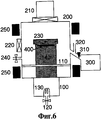
На фиг.6 дано схематическое изображение реализующей способ LEPEVPE системы, соответствующей данному изобретению, включающей дуговой плазмотрон постоянного тока и эффузионные ячейки.Figure 6 is a schematic representation of the LEPEVPE system implementing the system of this invention, including a direct current arc plasma torch and effusion cells.
Осуществление изобретенияThe implementation of the invention
Данное изобретение предлагает установку, а также устройство и способ, предназначенные для эпитаксиального выращивания полупроводников типа III-V, в частности нитридов группы III, таких как GaN, GaAlN, и GaInN. В устройстве генерируется низкотемпературная плазма высокой плотности, используемая в способе эпитаксии на полупроводниковой подложке полупроводниковых слоев осаждением из газовой фазы, активированной плазмой, Данная система позволяет экономически эффективно получать гетероструктуры, применимые в мощных высокочастотных усилителях, осветительных светодиодах, генерирующих фиолетовый, синий и белый свет, и полупроводниковых лазерах, генерирующих свет в синем и ультрафиолетовом диапазонах.The present invention provides an apparatus as well as an apparatus and method for the epitaxial growth of type III-V semiconductors, in particular Group III nitrides such as GaN, GaAlN, and GaInN. The device generates low-temperature high-density plasma, which is used in the method of epitaxy on a semiconductor substrate of semiconductor layers by plasma-activated gas vapor deposition. This system makes it possible to efficiently obtain heterostructures applicable in high-power high-frequency amplifiers, lighting LEDs generating violet, blue and white light, and semiconductor lasers that generate light in the blue and ultraviolet ranges.
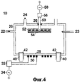
Обратимся теперь к фиг.1, где представлено устройство 10, в котором имеется вакуумная камера 20, имеющая внутреннее пространство 21, которое сообщается с системой вакуумной откачки (не показана), - например, системой, включающей турбомолекулярный вакуумный насос, - соединенной с выходной линией 24. Вакуумная камера 20 и система вакуумной откачки выбираются такими, чтобы были удовлетворены требования сверхвысокой чистоты, предъявляемые производством полупроводников. Было найдено, например, что таким требованиям удовлетворяет система, позволяющая получать (при отсутствии технологических газов) сверхвысокий вакуум. Инертные или нереакционноспособные при нормальных условиях газы, такие как аргон и азот, а также любые дополнительные газы, требуемые для протекания способа, поступают в вакуумную камеру 20 через средства 22 для ввода газов. Азот в форме N2 при обычных условиях является инертным. Но под воздействием плазменного поля данного средства молекулярный азот N2 превращается в атомарный азот (N) и становится высокоактивным и реакционноспособным. Вакуумная камера 20 имеет диэлектрическое окно 28, через которое электромагнитные волны высокочастотного диапазона (далее - "ВЧ") от блока спирального индуктора проступают во внутреннее пространство 21 вакуумной камеры 20. Блок 30 спирального индуктора соединен с цепью 32 согласования сопротивления и ВЧ-генератором 34. Электромагнитные волны ВЧ-диапазона, излучаемые спиральными витками индуктора, генерируют плотную низкотемпературную плазму во внутреннем пространстве 21 камеры 20. Так, например, показано, что ICP-плазмотрон "ICP-P 200", предлагаемый компанией JE PlasmaConsult, GmbH (г.Вупперталь, Германия), производит ионы аргона и азота с энергиями ниже 20 эВ, если он применяется при давлении в диапазоне от 10-4 до 10-2 мбар и при мощности до 1 киловатта.Turning now to FIG. 1, a
Блок 50 выращивания электрически изолирован от вакуумной камеры 20 с помощью изоляторов 26. Одна или несколько подложек 54 нагреваются с обратной стороны нагревателем 52, например омическим нагревателем или ламповыми нагревателями. Подложка 54 находится дальше от области самой высокой плотности плазмы, находящейся вблизи диэлектрического окна 28, - а именно дальше на расстояние, равное нескольким значениям глубины поверхностного слоя, обычно на 5-20 таких значений. Глубина поверхностного слоя составляет (по порядку величины) 1 см при типичных для данного изобретения значениях рабочего давления. Блок 50 выращивания может быть заземлен, но его потенциал может также оставаться "плавающим". Альтернативно, блок 50 выращивания может быть соединен с источником постоянного тока, обеспечивающим электрическое смещение, или может быть соединен через цепь 56 согласования сопротивления с ВЧ-генератором 58, благодаря чему будет происходить автоматическое смещение постоянного тока. Эти средства применяются для управления разностью потенциалов между подложками 54 и плазмой. Эти средства обеспечивают, что электрическая составляющая электромагнитного поля, перпендикулярная поверхности подложек 54, может регулироваться независимо от параметров, управляющих генерацией плазмы 36. Таким образом, энергию ионов, сталкивающихся с подложкой, можно регулировать, создавая оптимальные условия эпитаксии.The growing
Кроме того, вакуумная камера 20 имеет один или несколько эмиттеров 40 паров металлов (в воплощении, взятом в качестве иллюстрации, ими являются эффузионные ячейки), которые могут испарять металлы, - например, Ga, In и Al, - и инжектировать пары металлов во внутреннее пространство 21 камеры. Для подобных металлов температура эффузионных ячеек, обычно применяемых в молекулярно-лучевой эпитаксии (МВЕ), может быть легко установлена такой, что будут достигаться намного более высокие скорости испарения, чем обычные для этой технологии. Например, было найдено, что увеличение температуры эффузионной ячейки, испаряющей галлий, на 200°С оказывается достаточным для увеличения скорости нарастания слоя GaAs в 100 раз по сравнению со скоростью, типичной для способа МВЕ и составляющей 1 монослой/с. Как и для способа МВЕ, возможно управлять быстродействующими заслонками 42 так, чтобы полностью перекрывать потоки паров от эмиттеров 40.In addition, the
При эпитаксиальном осаждении мощность ВЧ-колебаний, подаваемых на индуктор 30, и давление газа в вакуумной камере 20 выбираются такими, что нагретые подложки 54 в полной мере подвергаются воздействию низкотемпературной плазмы. Обычно давление газа в вакуумной камере 20 лежит в диапазоне от 10-4 мбар до 1,0 мбар, а наиболее типичными являются значения в диапазоне от 10-2 до 10-1 мбар. При таких условиях перенос в плазме как активированного азота, так и паров металлов, поступающих от эффузионных ячеек 40, является диффузионным. Атомы металлов, реагируя с азотом, формируют эпитаксиальные слои нитридов на нагретых подложках 54.During epitaxial deposition, the power of the RF oscillations supplied to the
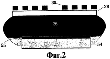
Обратимся теперь к фиг.2, где в деталях показан слой 55, выращиваемый на подложке 54, подвергаемой воздействию низкотемпературной плазмы 36. Плотность ионов плазмы экспоненциально убывает при удалении от диэлектрического окна 28 и приближении к подложке 54. Однако, например, для плазмотрона "ICP-P 200" плотность ионов азота в плазме может все еще превышать 1011 см-3 вблизи подложки, расположенной примерно на 10 см ниже диэлектрического окна 28, когда давление азота равно 10-1 мбар, интенсивность потока газа составляет 10 см3/мин, а мощность ВЧ-колебаний равна 1000 Вт. Для того чтобы значения энергии ионов оставались низкими, может оказаться полезным поддерживать полное давление газов постоянным, - например, вблизи значения 10-1 мбар, - обеспечивая поступление в вакуумную камеру через средство 22 ввода газов, наряду с газообразным азотом, регулируемого потока аргона, если парциальное давление азота выбирается существенно меньшим, чем 10-1 мбар.Turning now to FIG. 2, the
Благодаря эффективной активации реагентов в плотной плазме 36 и интенсивной бомбардировке поверхности подложки 54 ионами низкой энергии температура подложки может быть существенно понижена по сравнению с температурами, составляющими 1000°С и более, которые типичны для способа MOCVD. Поэтому можно ожидать, что значительно уменьшатся трудности, связанные с растрескиванием слоев, обусловленном различием коэффициентов теплового расширения наращиваемых слоев и типичных подложек (из сапфира, карбида кремния и кремния).Due to the effective activation of the reagents in
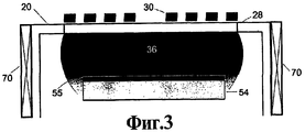
Обратимся теперь к фиг.3, на которой показана в деталях область вакуумной камеры 20, которая оборудована (но это не является обязательным) катушками или постоянными магнитами 70, служащими для удержания плазмы 36, а также для увеличения ее плотности и придания ей большей равномерности. Магнитное поле, создаваемое этими катушками или постоянными магнитами, помогает придать требуемую форму плазменному объему. Даже слабые поля, составляющие (по порядку величины) от 10-3 до 10-2 тесла, считаются дающими благоприятный эффект.We now turn to figure 3, which shows in detail the region of the
В предпочтительном воплощении изобретения при эпитаксиальном выращивании нитридных полупроводников совершенно не применяются химически активные газы. В дополнительных ячейках 40а могут помещаться различные легирующие примеси, которые предпочтительно применять в виде элементов, например, металлы (Mg, Zn и т.п.), проявляющие себя как акцепторные примеси. Точно так же с помощью дополнительных ячеек 40а могут вводиться легирующие вещества, ведущие себя как донорные примеси, например кремний. Такие эмиттеры (эффузионные ячейки) 40а также оснащаются быстродействующими затворами 42, позволяющими быстро и полностью перекрывать потоки легирующих примесей. Для того чтобы иметь возможность обработки пластин размером до 300 мм (и, потенциально, больших размеров), предпочтительно, чтобы в качестве материала для подложек 54 использовался кремний. Но с помощью нового способа, соответствующего изобретению, возможна также обработка подложек других типов, применяемых в технологиях, известных на данном техническом уровне.In a preferred embodiment of the invention, chemically active gases are not used at all in the epitaxial growth of nitride semiconductors. In additional cells 40a various alloying impurities can be placed, which are preferably used in the form of elements, for example, metals (Mg, Zn, etc.), which manifest themselves as acceptor impurities. In the same way, additional cells 40a can be used to introduce dopants behaving like donor impurities, such as silicon. Such emitters (effusion cells) 40a are also equipped with high-
Ранее никем не предлагалось сочетать применение эффузионных ячеек для распыления металлов с применением плотной низкотемпературной плазмы для эпитаксиального наращивания слоев. Мы называем новый способ "эпитаксией из газовой фазы, активированной низкотемпературной плазмой" (LEPEVPE). Способ LEPEVPE осуществляется при совершенно другихусловиях, чем условия во всех известных способах, включая способ LEPECVD, при котором для генерации плазмы применяется разряд постоянного тока, а исходные материалы являются химически активными газами.No one has previously proposed combining the use of effusion cells for sputtering metals with the use of dense low-temperature plasma for epitaxial layer growth. We call the new method "low temperature plasma activated epitaxy from the gas phase" (LEPEVPE). The LEPEVPE method is carried out under completely different conditions than the conditions in all known methods, including the LEPECVD method, in which a direct current discharge is used to generate plasma, and the starting materials are chemically active gases.
В одном воплощении изобретения область эмиттеров 300 паров имеет изолированную систему вакуумной откачки (320 на фиг.6), благодаря чему исключаются термические реакции с нагретыми до высоких температур металлами внутри камеры и диффузионный транспорт по соединительной трубке к вакуумной камере. В предпочтительном воплощении изобретения для каждого из испаряемых металлов предусмотрены несколько эмиттеров (эффузионных ячеек) 40 и 40а. Каждая ячейка может иметь свою рабочую температуру, что позволяет легко осуществлять быстрое изменение скорости роста и концентраций легирующих примесей переключением активности с одной ячейки на другую.In one embodiment of the invention, the
В другом воплощении изобретения применяются дополнительные подводящие газ линии 23, которые обеспечивают поступление в вакуумную камеру в газообразной форме таких легирующих элементов, которые предпочтительно применять в газообразной форме. Предпочтительно, чтобы легирующие примеси в газообразной форме, такие как кремневодород, применяемый как донорная примесь, были разбавлены инертным газом, например аргоном. Динамический диапазон характеристик легирования может быть расширен, если для введения одной легирующей примеси в газообразной форме использовать более чем одну подводящую газ линию. В предпочтительном воплощении, в котором эмиттеры 40а содержат только твердотельные источники легирующих примесей, способ осуществляется без участия водорода. Такое воплощение особенно предпочтительно при выращивании р-легированных слоев GaN, так как способ, в котором не участвует водород, не требует никакой активации легирующей примеси тепловым отжигом. Способ, соответствующий изобретению, осуществляется в отсутствие углерода, так как не требует никаких углеродосодержащих газообразных исходных веществ.In another embodiment of the invention, additional
В предпочтительном воплощении изобретения, которое иллюстрирует фиг.1, блок подложек 54 ориентирован поверхностью роста вверх. Такая конфигурация, обычно применяемая при изготовлении полупроводников, облегчает обработку пластин и упрощает конструкцию блока выращивания или подложкодержателя 50. Согласно изобретению способ LEPEVPE отличается тем, что низкотемпературная плазма высокой плотности находится в прямом контакте с поверхностью подложки 54. Поверхность подложки 54, следовательно, подвергается интенсивной бомбардировке низкоэнергетическими ионами, энергия которых может регулироваться соответствующим выбором потенциала смещения подложки. В этом состоит четкое отличие данного способа от способов плазменной обработки, использующих дистанцированные источники подачи плазмы, которые обычно дают только радикалы, тогда как плотности ионов на поверхности подложки пренебрежимо малы. Интенсивная бомбардировка подложки низкоэнергетическими ионами, как было показано, дает преимущества при эпитаксиальном выращивании слоев, предназначенных для качественных полупроводниковых приборов, при экстремально высоких скоростях роста, превышающих 5 нм/с и низких температурах подложки - столь низких, как, например, 500°С (см., например, публикацию von Kanel et al., Appl. Phys. Lett. 80, 2922 (2002), содержание которой включается посредством ссылки). Таким образом, согласно изобретению, можно ожидать, что очень высокая производительность будет достигаться, если сочетать способ LEPEVPE с отвечающими современному техническому уровню инструментальными средствами (не показаны) обработки пластин.In a preferred embodiment of the invention, which is illustrated in FIG. 1, the block of
Согласно данному изобретению устройство 10 может применяться для выращивания эпитаксиальных полупроводников III-V, в особенности - для выращивания нитридов элементов III группы на специально обработанных монокристаллических подложках 54. Возможные способы обработки поверхности подложек 54 могут включать отвечающие современному уровню техники способы предварительной химической очистки, термической или плазменной очистки, выполняемой in situ и сопровождаемой формированием in situ шаблонов для выращивания, например, состоящих из окислов, карбидов или осаждаемых при низких температурах нитридов, а далее применяемых для эпитаксиального наращивания на них полупроводниковых слоев нитридов.According to the present invention,
Обратимся теперь к фиг.4, на которой показана устройство 10 предлагаемой установки, где подложка 54, на которую производится осаждение, установлена на плате подложкодержателя 50 во внутреннем пространстве 21 камеры, причем подложки теперь ориентированы поверхностями роста вниз. При такой конфигурации возникает меньше трудностей, связанных с загрязнением макрочастицами, но требуется усложнение системы обработки пластин и конструкции подложкодержателя 50. Как отмечено выше, вакуумная камера 20 может быть (но это не обязательно) оснащена катушками индуктивности или постоянными магнитами, которые могут служить для придания нужной формы плазменному объему, и камера может быть оснащена эффузионными ячейками 40 и т.д., аналогично сказанному выше.Referring now to FIG. 4, the
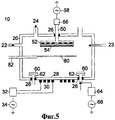
Обратимся теперь к фиг.5, на которой показано другое воплощение изобретения, где подложки 54, установленные в блоке выращивания 50 внутри камеры 20, как и выше, ориентированы поверхностями роста вниз. Вакуумная камера 20 может быть (но это не обязательно) оснащена катушками индуктивности или постоянными магнитами, которые могут служить для придания плазменному объему требуемой формы (см. фиг.3).Turning now to FIG. 5, another embodiment of the invention is shown, where
В этом воплощении пары металлов, представленных элементами, вводятся в плазму с помощью охлаждаемых водой источников 62 распыления, удерживающих мишени 60 для распыления. Желательно, чтобы мишени 60 для распыления были расположены как концентрические кольца или кольцевые сегменты вокруг диэлектрического окна 28 ICP-плазмотрона. Мишени для распыления соединены через блок 64 согласования сопротивления с блоком 66 питания ВЧ, который обеспечивает подачу периодически изменяющегося напряжения ВЧ; предпочтительно, чтобы его частота существенно отличалась от частоты генератора 34, служащего для питания катушек 30 ICP-плазмотрона. Это ослабляет нежелательную интерференцию между двумя видами источников питания - 34 и 66. В другом воплощении изобретения источники 62 распыления получают питание от блока питания постоянного тока. Показано, что для типичных значений произведения расстояния на давление, имеющих порядок 0,2·10-2 мбар·м термализация (уменьшение кинетической энергии) испаренных частиц, достигающих подложки, является почти полной, позволяющей применять источники распыления при выращивании материалов полупроводникового качества (см., например, публикацию Sutler et al., Appl. Phys. Lett., 67, 3954 (1995), содержание которой включается посредством ссылки). Чтобы обеспечить возможность перед эпитаксиальным выращиванием слоев очищать источники 62 распыления, камера 20 может быть (но это не обязательно) оборудована подвижным экранирующим средством 82, позволяющим располагать экран 80 средства вблизи подложек 54 и ниже их, что предотвращает попадание на подложку частиц испаренных веществ в период разогрева.In this embodiment, the metal vapors represented by the elements are introduced into the plasma using water-cooled
В предпочтительном воплощении изобретения при эпитаксиальном выращивании нитридных полупроводников не применяются никакие химически активные газы. Дополнительные мишени 60а для распыления могут содержать легирующие вещества, которые предпочтительно использовать в элементной форме, - например, металлы Mg, Zn и т.п., играющие роль акцепторных примесей. Точно так же с помощью дополнительных мишеней 60а для распыления могут вводиться легирующие вещества, играющие роль донорных примесей, например кремний. В другом воплощении изобретения каждая пушка 62 для распыления может быть (но это не обязательно) снабжена заслонками (не показаны), позволяющими избежать взаимного загрязнения мишеней 60.In a preferred embodiment of the invention, no reactive gases are used in the epitaxial growth of nitride semiconductors. Additional sputtering targets 60a may contain dopants that are preferably used in elemental form — for example, Mg, Zn metals and the like, which act as acceptor impurities. Likewise, with the aid of additional sputtering targets 60a, dopants that play the role of donor impurities, such as silicon, can be introduced. In another embodiment of the invention, each
В процессе эпитаксиального выращивания на индуктор 30 подается питание ВЧ такой частоты, а давление газа в вакуумной камере 20 выбирается таким, что нагретые подложки 54 в полной мере подвергаются воздействию низкотемпературной плазмы. Типичные значения давлений в вакуумной камере 20 лежат в диапазоне от 10-3 мбар до 10-1 мбар, а наиболее типичны значения в диапазоне от 10-2 до 10-1 мбар. При указанных условиях как активированный азот, так и пары металлов от пушек 62 для распыления распространяются в плазме диффузионным переносом, и процесс происходит так, как описано выше.During epitaxial growth, an RF power of such a frequency is supplied to the
В другом воплощении изобретения пушки 62 для распыления могут сочетаться с эффузионными ячейками 40; при этом предпочтительно, чтобы источники обоих типов были расположены симметрично вокруг диэлектрического окна 28. Ранее не предлагалось для эпитаксиального наращивания слоев сочетать применение эффузионных ячеек и пушек для распыления (служащих для испарения реагентов и легирующих примесей в элементной форме) с применением плотной низкотемпературной плазмы. В предпочтительном воплощении изобретения любой из металлов может испаряться с помощью нескольких пушек 62 для распыления и эффузионных ячеек 40. Каждый источник может иметь собственное значение интенсивности потока паров одного и того же металла, что позволяет легко осуществлять быстрые вариации скоростей роста и концентраций легирующих примесей путем переключения активности с одного источника на другой. В еще одном воплощении эффузионные ячейки 40 и пушки 62 для распыления могут быть заменены или дополнены электронно-лучевыми испарителями. Электронно-лучевые испарители дают особенно большие преимущества при испарении элементов, пары которых имеют низкое давление, так как в этом случае трудно достичь значительных величин потоков, если применять эффузионные ячейки 40.In another embodiment of the invention,
Обратимся теперь к фиг.6, где представлено другое воплощение изобретения, в котором устройство 10 включает источник 100 подачи плазмы, создающий широкую область горения плазмы, включающий блок термокатодов 130, средство 120 ввода инертного газа и интегрированный или изолированный анод 110. Предпочтительно, чтобы разность потенциалов между катодами 130 и анодом 110 была меньшей, чем 30 V, благодаря чему обеспечивается, что сталкивающиеся с подложкой ионы обладают энергией, меньшей, чем примерно 20 эВ. Плазмотрон 100, генерирующий плазму 140 с помощью дугового разряда, соединен с вакуумной камерой 200. В вакуумной камере, оборудованной загрузочным шлюзом 220, создается вакуум, - с помощью, например, турбомолекулярного насоса 210, соединенного с камерой 200 через клапан 205; в камере находится блок 230 нагрева подложек. К вакуумной камере присоединены подводящие газ линии 240 для ввода инертного газа, например азота, и дополнительных газов, например водорода. Плотность плазмы может быстро варьироваться с помощью изменения удерживающего магнитного поля, создаваемого катушками 250.Referring now to FIG. 6, another embodiment of the invention is presented in which the
Кроме того, данная камера оборудована эффузионными ячейками 300, из которых могут испаряться металлы, такие как Ga и Al. В дополнительных ячейках 300 могут содержаться такие виды легирующих примесей, которые предпочтительно применять в виде элементов, - например, металлы (Mg, Zn и т.п.), действующие как акцепторные примеси. Эффузионные ячейки оборудованы затворами 310, позволяющими полностью перекрывать поступление паров металлов.In addition, this chamber is equipped with
Нагретый блок подложек 400 в полной мере подвергается воздействию низкотемпературной плазмы, генерируемой дуговым разрядом плазмотрона и распространяющейся в вакуумную камеру через проницаемый анод 110. Дуговой разряд поддерживается термокатодами 130 в плазменной камере 200; он может поддерживаться при значениях давления в вакуумной камере, лежащих в широком диапазоне - от 10-4 мбар до, по крайней мере, 10-1 мбар, а наиболее типичны значения давления, примерно равные 10-2 мбар. Активированный плазмой азот, поток которого проходит через вакуумную камеру, реагирует с парами металлов, формируя эпитаксиальную пленку нитрида на подложке 400.The heated block of
Для испарения металлов в сверхвысоком вакууме, например в системах для молекулярной эпитаксии, обычно применяют эффузионные ячейки. В данном случае они служат для ввода паров металлов в низкотемпературную плазму высокой плотности, которая генерируется при давлениях, типичные значения которых составляют примерно 10-2 мбар, при которых перенос вещества является диффузионным. Способ LEPEVPE, следовательно, является способом, протекающим при совершенно других условиях, чем другие способы. В одном воплощении изобретения область эффузионных ячеек 300 снабжена отдельной системой 320 вакуумной откачки с целью исключить тепловые реакции с нагретыми металлами внутри камеры и диффузионный перенос по соединительной трубке к вакуумной камере.For the evaporation of metals in ultrahigh vacuum, for example in systems for molecular epitaxy, effusion cells are usually used. In this case, they serve to introduce metal vapors into a low-temperature high-density plasma, which is generated at pressures whose typical values are about 10 -2 mbar, at which the substance transfer is diffusive. The LEPEVPE method, therefore, is a method proceeding under completely different conditions than other methods. In one embodiment of the invention, the region of the
В предпочтительном воплощении изобретения для ввода каждого из испаряемых металлов может использоваться более чем одна эффузионная ячейка 300. Все такие ячейки могут функционировать при различных температурах, благодаря чему можно легко осуществлять быстрые изменения скоростей роста и концентраций легирующих примесей с помощью переключения активности с одной ячейки на другую. Кроме того, управление плотностью плазмы с помощью изменений магнитного поля, создаваемого катушками 250, может еще более расширить пределы динамических диапазонов скоростей роста.In a preferred embodiment of the invention, more than one
В другом воплощении изобретения дополнительные подводящие газ линии 240а служат для поступления в вакуумную камеру в газообразной форме таких легирующих элементов, которые предпочтительно применять в газообразной форме. Предпочтительно, чтобы газообразные легирующие примеси, такие как кремневодород, применяемый для легирования донорной примесью, были разбавлены инертным газом, например аргоном. Динамический диапазон характеристик легирования может быть расширен, если для введения одной газообразной легирующей примеси применять более одной подводящей газ линии.In another embodiment of the invention, the additional gas supply lines 240a are used to introduce such alloying elements into the vacuum chamber in gaseous form that are preferably used in gaseous form. Preferably, gaseous dopants, such as silica used for doping with a donor impurity, are diluted with an inert gas, such as argon. The dynamic range of doping characteristics can be expanded if more than one gas supply line is used to introduce one gaseous dopant.
В способе, предлагаемом в изобретения, не участвует углерод, так как не требуются никакие углеродсодержащие газообразные исходные вещества. В предпочтительном воплощении способ осуществляется, кроме того, при отсутствии водорода. Такое воплощение является особенно предпочтительным при выращивании р-легированных слоев GaN, так как для способов без участия водорода не требуется никакой активации легирующих примесей тепловым отжигом. Так как способ LEPEVPE является способом, активируемым плазмой, он может осуществляться при более низких температурах подложки, чем температуры, характерные для сравниваемых способов, применяемых для аналогичных целей; при использовании этих способов механическое напряжение, обусловленное различием коэффициентов теплового расширения материалов эпитаксиального слоя и подложки, часто приводит к нежелательному трещинообразованию при охлаждении от температуры выращивания до обычной температуры.Carbon is not involved in the process of the invention, since no carbonaceous gaseous starting materials are required. In a preferred embodiment, the process is further carried out in the absence of hydrogen. Such an embodiment is particularly preferred when growing p-doped GaN layers, since for methods without the participation of hydrogen, no activation of the dopants by thermal annealing is required. Since the LEPEVPE method is a plasma activated method, it can be carried out at lower substrate temperatures than the temperatures characteristic of the compared methods used for similar purposes; when using these methods, mechanical stress due to the difference in the thermal expansion coefficients of the materials of the epitaxial layer and the substrate often leads to undesirable cracking upon cooling from the temperature of cultivation to normal temperature.
ПРИЛОЖЕНИЕ А. Данный документ опирается на следующие документы, включаемые посредством ссылок.ANNEX A. This document is based on the following documents, incorporated by reference.
Патентные документы СШАUS Patent Documents
6,472,300 10/2002 Nikolaev et al.6,472,300 10/2002 Nikolaev et al.
6,706,119 3/2004 Tsvetkov et al.6,706,119 3/2004 Tsvetkov et al.
6,818,061 11/2004 Peczalski et al.6,818,061 11/2004 Peczalski et al.
5,633,192 5/1997 Moustakas et al.5,633,192 5/1997 Moustakas et al.
6,454,855 9/2002 von Kanel et al.6,454,855 9/2002 von Kanel et al.
6,918,352 7/2005 von Kanel et al.6,918,352 7/2005 von Kanel et al.
5,580,420 12/1996 Watanabe et al.5,580,420 12/1996 Watanabe et al.
4,368,092 1/1983 Steinberg et al.4,368,092 1/1983 Steinberg et al.
4,948,458 8/1990 Ogle4,948,458 8/1990 Ogle
6,811,611 11/2004 Johnson6,811,611 11/2004 Johnson
5,788,799 8/1998 Steger et al.5,788,799 8/1998 Steger et al.
Другие патентные документыOther patent documents
WO 2006/000846 1/2006 von Kanel et al.WO 2006/000846 1/2006 von Kanel et al.
Дополнительные публикацииAdditional publications
J.D. Brown et al., "Гетероструктурные полевые транзисторы на основе AlGaN/GaN, полученные на 100-миллиметровых подложках GaN, выращенных на кремниевых (111) подложках", Solid-State Electronics, Vol.46, No. 10 (October 2002) pp.1535-1539.J.D. Brown et al., "AlGaN / GaN-Based Heterostructured Field-Effect Transistors Obtained on 100 mm GaN Substrates Raised on Silicon (111) Substrates", Solid-State Electronics, Vol. 46, No. 10 (October 2002) pp. 1535-1539.
S. Nakamura, "Лазерные диоды на основе InGaN", Annual Reviews on Material Science, Vol.28 (1998) pp.125-152.S. Nakamura, "InGaN Based Laser Diodes," Annual Reviews on Material Science, Vol. 28 (1998) pp. 125-152.
S. Nakamura, "Роль структурных дефектов в генерирующих синий свет светодиодах и лазерных диодах на основе InGaN", Science, Vol.281 (14 August 1998) pp.956-961.S. Nakamura, "The Role of Structural Defects in BlueGenerating LEDs and Laser Diodes Based on InGaN," Science, Vol. 281 (August 14, 1998) pp.956-961.
G.A. Smith et al., "Эмиссия излучения с длиной волны 341 нм ультрафиолетовыми светодиодами, выращенными гидридной эпитаксией из газовой фазы", Journal of Applied Physics, Vol.95, No. 12 (15 June 2004) pp.8247-8251.G.A. Smith et al., “Emission of 341 nm radiation by ultraviolet LEDs grown by hydride epitaxy from the gas phase”, Journal of Applied Physics, Vol. 95, No. 12 (June 15, 2004) pp. 8247-8251.
R.F. Davis et al., "Материалы на основе нитрида галлия: успехи, современное состояние и потенциальные проблемы". Proceedings of the IEEE, Vol.90, No. 6 (June 2002) pp.993-1004.R.F. Davis et al., "Materials Based on Gallium Nitride: Advances, Current Status and Potential Problems." Proceedings of the IEEE, Vol. 90, No. 6 (June 2002) pp. 993-1004.
A. Dadgar et al., "Химическая эпитаксия на кремний нитрида галлия из газовой фазы металлоорганических материалов", physica status solidi (с), Vol.0, No. 6 (September 2003) pp.1583-1606.A. Dadgar et al., “Chemical Epitaxy on Silicon Gallium Nitride from the Gas Phase of Organometallic Materials”, physica status solidi (c), Vol.0, No. 6 (September 2003) pp. 1583-1606.
Т. Wang et al., "Подвижность электронов, превышающая 104 см2/Вс в одной гетероструктуре AlGaN-GaN, выращенной на сапфировой подложке", Applied Physics Letters, Volume 74, No. 23 (7 June 1999) pp.3531-3533.T. Wang et al., "Electron mobility in excess of 10 4 cm 2 / Vc in a single AlGaN-GaN heterostructure grown on a sapphire substrate", Applied Physics Letters, Volume 74, No. 23 (June 7, 1999) pp. 3531-3533.
J. Blasing et al., "Первопричины уменьшения напряжения, обусловленного наличием низкотемпературных промежуточных слоев AlN", Applied Physics Letters, Vol.81, No. 15 (7 October 2002) pp.2722-2724.J. Blasing et al., "Root Causes of Stress Reduction Due to Low-Temperature AlN Intermediate Layers", Applied Physics Letters, Vol. 81, No. 15 (October 7, 2002) pp. 2722-2724.
С.R. Elsass, "Перенос электронов в гетероструктурах AlGaN/GaN, выращиваемых с помощью молекулярно-лучевой эпитаксии с участием плазмы", Japanese Journal of Applied Physics, Vol.39, Part 2, No. 10B (15 October 2000) pp. L1023-L1025.C.R. Elsass, "Electron transport in AlGaN / GaN heterostructures grown by plasma-beam molecular beam epitaxy," Japanese Journal of Applied Physics, Vol. 39, Part 2, No. 10B (October 15, 2000) pp. L1023-L1025.
C. Rosenblad et al., "Эпитаксия кремния химическим осаждением из газовой фазы, активированной низкотемпературной плазмой", Journal of Vacuum Science and Technology A, Vol.16, No. 5 (Sept/Oct 1998), pp.2785-2790.C. Rosenblad et al., "Silicon Epitaxy by Chemical Precipitation Activated by Low Temperature Plasma", Journal of Vacuum Science and Technology A, Vol.16, No. 5 (Sept / Oct 1998), pp. 2785-2790.
Heung-Sik Tae et al., "Низкотемпературная гомоэпитаксия кремния химическим осаждением из газовой фазы с использованием электронного циклотронного резонанса в сверхвысоком вакууме", Applied Physics Letters, Vol.64, No. 8 (21 February 1994) pp.1021-1023.Heung-Sik Tae et al., "Low Temperature Homoepitaxy of Silicon by Chemical Vapor Deposition Using Electron Cyclotron Resonance in Ultrahigh Vacuum", Applied Physics Letters, Vol. 64, No. 8 (February 21, 1994) pp. 1021-1023.
С.В. Vartuli et al., "Плазменное травление в ICl/Ar нитридов типа III-V с использованием электронного циклотронного резонанса", Applied Physics Letters, Vol.69, No. 10 (2 September 1996), pp.1426-1428.S.V. Vartuli et al., "Plasma Etching in ICl / Ar of Type III-V Nitrides Using Electron Cyclotron Resonance", Applied Physics Letters, Vol.69, No. 10 (2 September 1996), pp. 1426-1428.
W.Z. Collison et al., "Исследования плазменного травления пластин большого диаметра с использованием индуктивно-связанных источников подачи плазмы низкого давления, выполненные с применением моделирования плазмы и ленгмюровского зонда", Journal of Vacuum Science and Technology A, Vol.16, No. 1 (Jan/Feb 1998), pp.100-107.W.Z. Collison et al., “Plasma Etching of Large Diameter Plates Using Inductively Coupled Low Pressure Plasma Sources Using Plasma and Langmuir Probe Simulations,” Journal of Vacuum Science and Technology A, Vol.16, No. 1 (Jan / Feb 1998), pp. 100-107.
R.J. Shul et al., "Плазменное травление GaN индуктивно-связанной плазмой", Applied Physics Letters, Vol.69, No. 8 (19 August 1996), pp.1119-1121.R.J. Shul et al., "Plasma Etching of GaN Inductively Coupled Plasma", Applied Physics Letters, Vol.69, No. 8 (August 19, 1996), pp. 1119-1121.
J. Hopwood, "Обзор видов индуктивно-связанной плазмы, применимых для плазменной обработки", Plasma Source Science and Technology, Vol.1, No. 2 (May 1992) pp.109-116.J. Hopwood, “Overview of Inductively Coupled Plasma Applicable for Plasma Processing,” Plasma Source Science and Technology, Vol. 1, No. 2 (May 1992) pp. 109-116.
D.S.Green et al., Легирование углеродом GaN посредством CBr4 при молекулярно-лучевой эпитаксии с участием плазмы, генерируемой ВЧ-плазмотроном", Journal of Applied Physics, Vol.95, No. 12 (15 June 2004) pp.8456-8462.DSGreen et al., Carbon Doping of GaN with CBr 4 in Molecular Beam Epitaxy with a Plasma Generated by an RF Plasmatron, "Journal of Applied Physics, Vol. 95, No. 12 (June 15, 2004) pp.8456-8462.
H. von Kanel, "Очень высокая подвижность дырок в квантовых ямах неоднородно легированного Ge, выращенных способом химического осаждения из газовой фазы, активированной низкотемпературной плазмой", Applied Physics Letters, Vol.80, No. 16 (22 April 2002), pp.2922-2924.H. von Kanel, "Very high mobility of holes in quantum wells of heterogeneously doped Ge grown by chemical vapor deposition by low-temperature plasma," Applied Physics Letters, Vol.80, No. 16 (April 22, 2002), pp. 2922-2924.
P. Sutter et al., "Квантовый перенос в гетероструктурах Si/Si1-xGex, получаемых испарением и эпитаксией", Applied Physics Letters, Vol.67, No. 26 (25 December 1995), pp.3954-3956.P. Sutter et al., "Quantum Transfer in Si / Si 1-x Ge x Heterostructures Obtained by Evaporation and Epitaxy", Applied Physics Letters, Vol. 67, No. 26 (25 December 1995), pp. 3954-3956.
Claims (31)
Applications Claiming Priority (2)
| Application Number | Priority Date | Filing Date | Title |
|---|---|---|---|
| US65720805P | 2005-02-28 | 2005-02-28 | |
| US60/657,208 | 2005-02-28 |
Publications (2)
| Publication Number | Publication Date |
|---|---|
| RU2007135977A RU2007135977A (en) | 2009-04-10 |
| RU2462786C2 true RU2462786C2 (en) | 2012-09-27 |
Family
ID=36972965
Family Applications (1)
| Application Number | Title | Priority Date | Filing Date |
|---|---|---|---|
| RU2007135977/28A RU2462786C2 (en) | 2005-02-28 | 2006-02-28 | Method and apparatus for epitaxial growth of type iii-v semiconductors, apparatus for generating low-temperature high-density plasma, epitaxial metal nitride layer, epitaxial metal nitride heterostructure and semiconductor |
Country Status (10)
| Country | Link |
|---|---|
| US (2) | US8647434B2 (en) |
| EP (1) | EP1872383A2 (en) |
| JP (1) | JP5214251B2 (en) |
| KR (2) | KR101358966B1 (en) |
| CN (1) | CN101128911B (en) |
| AU (1) | AU2006224282B2 (en) |
| CA (1) | CA2597623C (en) |
| RU (1) | RU2462786C2 (en) |
| SG (1) | SG160345A1 (en) |
| WO (1) | WO2006097804A2 (en) |
Cited By (7)
| Publication number | Priority date | Publication date | Assignee | Title |
|---|---|---|---|---|
| RU2548578C2 (en) * | 2013-08-19 | 2015-04-20 | Валерий Анатольевич Буробин | Method of obtaining epitaxial layer of binary semiconductor material on monocrystalline substrate by organometallic chemical vapour deposition |
| RU2570099C1 (en) * | 2014-08-05 | 2015-12-10 | Акционерное общество "Научно-производственное предприятие "Исток" имени А.И. Шокина" (АО "НПП "Исток" им. Шокина") | Manufacturing method of semiconductor heterostructure |
| RU2578870C2 (en) * | 2014-03-26 | 2016-03-27 | Открытое акционерное общество "Ордена Трудового Красного Знамени Научно-исследовательский физико-химический институт им. Л.Я. Карпова" (ОАО "НИФХИ им. Л.Я. Карпова") | Method of growing gallium nitride film |
| RU2653118C1 (en) * | 2014-08-29 | 2018-05-07 | Соко Кагаку Ко., Лтд. | Template for epitaxial growth, a method for producing it and a nitride semiconductor device |
| RU2715080C1 (en) * | 2018-12-18 | 2020-02-25 | Федеральное государственное бюджетное учреждение науки Физический институт им. П.Н. Лебедева Российской академии наук (ФИАН) | Method of monocrystalline layers of semiconductor structures growth |
| RU2723477C1 (en) * | 2019-04-26 | 2020-06-11 | Федеральное государственное автономное образовательное учреждение высшего образования "Национальный исследовательский Нижегородский государственный университет им. Н.И. Лобачевского" | Unit for fixation of heated substrate in vacuum chamber (embodiments) |
| RU2796363C1 (en) * | 2022-07-26 | 2023-05-22 | Акционерное общество "Научно-производственное предприятие "Пульсар" | Method for diagnostics of composition and crystallographic parameters of semiconductor epitaxial heterostructures |
Families Citing this family (28)
| Publication number | Priority date | Publication date | Assignee | Title |
|---|---|---|---|---|
| EP1513233B1 (en) * | 2003-09-05 | 2008-10-29 | Epispeed S.A. | InGaAs/GaAs lasers on Silicon produced by LEPECVD and MOCVD |
| KR100754404B1 (en) * | 2006-05-25 | 2007-08-31 | 삼성전자주식회사 | Diffusion tube, dopant source for process of diffusion, and the method of diffusion using the diffusion tube and the dopant source |
| JP5041883B2 (en) * | 2007-06-07 | 2012-10-03 | 昭和電工株式会社 | Method for producing group III nitride semiconductor layer, method for producing group III nitride semiconductor light emitting device |
| JP4982259B2 (en) * | 2007-06-14 | 2012-07-25 | 昭和電工株式会社 | Method for manufacturing group III nitride compound semiconductor light emitting device |
| EP2207911A1 (en) * | 2007-08-17 | 2010-07-21 | Epispeed S.A. | Apparatus and method for producing epitaxial layers |
| US20110174213A1 (en) | 2008-10-03 | 2011-07-21 | Veeco Compound Semiconductor, Inc. | Vapor Phase Epitaxy System |
| CN101494151B (en) * | 2009-03-05 | 2013-11-13 | 苏州晶能科技有限公司 | Magnetic control cathode assembly for cleaning one-dimensional linear plasma with high efficiency |
| JP2011213557A (en) * | 2010-04-01 | 2011-10-27 | Hitachi Cable Ltd | Method for producing conductive group iii nitride single crystal substrate |
| TWI562195B (en) | 2010-04-27 | 2016-12-11 | Pilegrowth Tech S R L | Dislocation and stress management by mask-less processes using substrate patterning and methods for device fabrication |
| US8884525B2 (en) * | 2011-03-22 | 2014-11-11 | Advanced Energy Industries, Inc. | Remote plasma source generating a disc-shaped plasma |
| DE102012201953A1 (en) * | 2012-02-09 | 2013-08-14 | Singulus Technologies Ag | Method and device for passivation of solar cells with an aluminum oxide layer |
| CN102534511B (en) * | 2012-02-28 | 2013-10-16 | 东北大学 | Film vapor deposition device and application method thereof |
| JP6235581B2 (en) * | 2012-07-13 | 2017-11-22 | ガリウム エンタープライジズ ピーティーワイ リミテッド | Film forming apparatus and method |
| KR101456549B1 (en) * | 2012-09-10 | 2014-10-31 | 한국표준과학연구원 | Plassma Enhanced Chemical Vapour Deposition Apparatus And Plassma Enhanced Chemical Vapour Deposition Method |
| US9378941B2 (en) | 2013-10-02 | 2016-06-28 | Applied Materials, Inc. | Interface treatment of semiconductor surfaces with high density low energy plasma |
| CN104752162A (en) * | 2013-12-31 | 2015-07-01 | 江西省昌大光电科技有限公司 | Semi-insulated GaN film and preparation method thereof |
| CN103806093B (en) * | 2014-02-17 | 2017-01-18 | 清华大学 | Epitaxial growth device and method for ICP (inductively coupled plasma) based compound semiconductor |
| CN103938272A (en) * | 2014-04-03 | 2014-07-23 | 清华大学 | Plasma assisted epitaxial growth device and method |
| WO2018081144A1 (en) | 2016-10-24 | 2018-05-03 | Kla-Tencor Corporation | Process module(s) integrated into a metrology and/or inspection tool |
| WO2019005144A1 (en) * | 2017-06-30 | 2019-01-03 | Intel Corporation | High throughput molecular beam epitaxy and apparatus for selective epitaxy |
| RU2657674C1 (en) * | 2017-08-14 | 2018-06-14 | Федеральное государственное бюджетное учреждение науки Институт общей и неорганической химии им. Н.С. Курнакова Российской академии наук (ИОНХ РАН) | METHOD FOR PRODUCING HETEROSTRUCTURE Mg(Fe1-XGaX)2O4/SI WITH STABLE INTERPHASE BOUNDARY |
| CN107675141B (en) * | 2017-10-25 | 2023-08-04 | 南昌大学 | Device for preparing nitride material |
| US10892137B2 (en) * | 2018-09-12 | 2021-01-12 | Entegris, Inc. | Ion implantation processes and apparatus using gallium |
| DE102018220678A1 (en) * | 2018-11-30 | 2020-06-04 | Thyssenkrupp Ag | Process for PVD coating workpieces |
| CN109817518B (en) * | 2019-01-18 | 2020-03-10 | 重庆市妙格科技有限公司 | Phosphor expanding device for heating raw materials of light-emitting diode |
| CN109830419B (en) * | 2019-01-24 | 2020-05-19 | 中国原子能科学研究院 | Miniature penning ion source |
| WO2020215189A1 (en) * | 2019-04-22 | 2020-10-29 | Peng Du | Mbe system with direct evaporation pump to cold panel |
| US11150120B2 (en) * | 2019-09-22 | 2021-10-19 | Applied Materials, Inc. | Low temperature thermal flow ratio controller |
Citations (1)
| Publication number | Priority date | Publication date | Assignee | Title |
|---|---|---|---|---|
| RU2244984C1 (en) * | 2003-08-08 | 2005-01-20 | Институт физики полупроводников Объединенного института физики полупроводников СО РАН | Heterostructure manufacturing process |
Family Cites Families (21)
| Publication number | Priority date | Publication date | Assignee | Title |
|---|---|---|---|---|
| US4368092A (en) | 1981-04-02 | 1983-01-11 | The Perkin-Elmer Corporation | Apparatus for the etching for semiconductor devices |
| JPH0652716B2 (en) * | 1984-08-24 | 1994-07-06 | 日本電信電話株式会社 | Semiconductor crystalline film manufacturing equipment |
| JPS61135126A (en) * | 1984-12-06 | 1986-06-23 | Hitachi Ltd | Equipment of plasma treatment |
| US4948458A (en) | 1989-08-14 | 1990-08-14 | Lam Research Corporation | Method and apparatus for producing magnetically-coupled planar plasma |
| JPH03146656A (en) * | 1989-11-02 | 1991-06-21 | Hitachi Ltd | Method and device for film formation |
| US5633192A (en) | 1991-03-18 | 1997-05-27 | Boston University | Method for epitaxially growing gallium nitride layers |
| KR100321325B1 (en) | 1993-09-17 | 2002-06-20 | 가나이 쓰도무 | Plasma generation method and apparatus and plasma processing method and apparatus using the same |
| JPH07288237A (en) | 1994-04-15 | 1995-10-31 | Nippon Steel Corp | Plasma exciting cell apparatus |
| US5783101A (en) | 1994-09-16 | 1998-07-21 | Applied Materials, Inc. | High etch rate residue free metal etch process with low frequency high power inductive coupled plasma |
| JP3769059B2 (en) * | 1996-02-02 | 2006-04-19 | 雅弘 西川 | Ultrasonic / plasma / particle beam combined process apparatus, thin film forming method and surface smoothing method |
| US5788799A (en) | 1996-06-11 | 1998-08-04 | Applied Materials, Inc. | Apparatus and method for cleaning of semiconductor process chamber surfaces |
| JPH1012908A (en) * | 1996-06-21 | 1998-01-16 | Toshiba Corp | Manufacture of semiconductor device and particulate semiconductor film, and photoelectric conversion element |
| EP0988407B9 (en) | 1997-06-13 | 2004-12-15 | Unaxis Trading AG | Method for producing coated workpieces, which are coated with an epitactic layer |
| US6472300B2 (en) | 1997-11-18 | 2002-10-29 | Technologies And Devices International, Inc. | Method for growing p-n homojunction-based structures utilizing HVPE techniques |
| WO2001065590A2 (en) | 2000-03-02 | 2001-09-07 | Tokyo Electron Limited | Esrf source for ion plating epitaxial deposition |
| US6656272B2 (en) | 2001-03-30 | 2003-12-02 | Technologies And Devices International, Inc. | Method of epitaxially growing submicron group III nitride layers utilizing HVPE |
| US6992011B2 (en) | 2003-01-15 | 2006-01-31 | Tokyo Electron Limited | Method and apparatus for removing material from chamber and wafer surfaces by high temperature hydrogen-containing plasma |
| JP2004288964A (en) * | 2003-03-24 | 2004-10-14 | Sumitomo Electric Ind Ltd | PROCESS FOR GROWING GaN CRYSTAL |
| US6818061B2 (en) | 2003-04-10 | 2004-11-16 | Honeywell International, Inc. | Method for growing single crystal GaN on silicon |
| ES2380699T3 (en) | 2004-06-08 | 2012-05-17 | Dichroic Cell S.R.L. | System for chemical deposition in low-energy plasma assisted vapor phase |
| WO2008000846A1 (en) | 2006-06-19 | 2008-01-03 | Natraceutical S.A. | Method for sterilizing cocoa materials using supercritical co2 |
-
2006
- 2006-02-28 CA CA2597623A patent/CA2597623C/en not_active Expired - Fee Related
- 2006-02-28 JP JP2007557614A patent/JP5214251B2/en not_active Expired - Fee Related
- 2006-02-28 WO PCT/IB2006/000421 patent/WO2006097804A2/en active Application Filing
- 2006-02-28 EP EP06755827A patent/EP1872383A2/en not_active Withdrawn
- 2006-02-28 CN CN2006800063432A patent/CN101128911B/en not_active Expired - Fee Related
- 2006-02-28 RU RU2007135977/28A patent/RU2462786C2/en not_active IP Right Cessation
- 2006-02-28 AU AU2006224282A patent/AU2006224282B2/en not_active Ceased
- 2006-02-28 KR KR1020127009425A patent/KR101358966B1/en not_active IP Right Cessation
- 2006-02-28 US US11/817,208 patent/US8647434B2/en not_active Expired - Fee Related
- 2006-02-28 SG SG201001337-3A patent/SG160345A1/en unknown
- 2006-02-28 KR KR1020077021605A patent/KR101366181B1/en not_active IP Right Cessation
-
2013
- 2013-03-11 US US13/792,238 patent/US9466479B2/en not_active Expired - Fee Related
Patent Citations (1)
| Publication number | Priority date | Publication date | Assignee | Title |
|---|---|---|---|---|
| RU2244984C1 (en) * | 2003-08-08 | 2005-01-20 | Институт физики полупроводников Объединенного института физики полупроводников СО РАН | Heterostructure manufacturing process |
Non-Patent Citations (1)
| Title |
|---|
| RUBIN M ET AL. P-TYPE GALLIUM NITRIDE BY REACTIVE ION-BEAM MOLECULAR BEAM EPITAXY WITH ION IMPLANTATION, DIFFUSION. OR COEVAPORATION OF MG. APPLIED PHYSICS LETTERS, AIP, AMERICAN INSTITUTE OF PHYSICS, MELVILLE, NY, US, v.64, №1, 3 January 1994 (1994-01-03), p.64-66. LEI T FT AL. EPITAXIAL GROWTH OF ZINC BLENDE AND WURTZITIC GALLIUM NITRIDE THIN FILMS ON (001) SILICON. APPLIED PHYSICS LETTERS. AIP. AMERICAN INSTITUTE OF PHYSICS, MELVILLE, NY, US, v.59, №8.19 August 1991 (1991-08-19), p.944-946. * |
Cited By (7)
| Publication number | Priority date | Publication date | Assignee | Title |
|---|---|---|---|---|
| RU2548578C2 (en) * | 2013-08-19 | 2015-04-20 | Валерий Анатольевич Буробин | Method of obtaining epitaxial layer of binary semiconductor material on monocrystalline substrate by organometallic chemical vapour deposition |
| RU2578870C2 (en) * | 2014-03-26 | 2016-03-27 | Открытое акционерное общество "Ордена Трудового Красного Знамени Научно-исследовательский физико-химический институт им. Л.Я. Карпова" (ОАО "НИФХИ им. Л.Я. Карпова") | Method of growing gallium nitride film |
| RU2570099C1 (en) * | 2014-08-05 | 2015-12-10 | Акционерное общество "Научно-производственное предприятие "Исток" имени А.И. Шокина" (АО "НПП "Исток" им. Шокина") | Manufacturing method of semiconductor heterostructure |
| RU2653118C1 (en) * | 2014-08-29 | 2018-05-07 | Соко Кагаку Ко., Лтд. | Template for epitaxial growth, a method for producing it and a nitride semiconductor device |
| RU2715080C1 (en) * | 2018-12-18 | 2020-02-25 | Федеральное государственное бюджетное учреждение науки Физический институт им. П.Н. Лебедева Российской академии наук (ФИАН) | Method of monocrystalline layers of semiconductor structures growth |
| RU2723477C1 (en) * | 2019-04-26 | 2020-06-11 | Федеральное государственное автономное образовательное учреждение высшего образования "Национальный исследовательский Нижегородский государственный университет им. Н.И. Лобачевского" | Unit for fixation of heated substrate in vacuum chamber (embodiments) |
| RU2796363C1 (en) * | 2022-07-26 | 2023-05-22 | Акционерное общество "Научно-производственное предприятие "Пульсар" | Method for diagnostics of composition and crystallographic parameters of semiconductor epitaxial heterostructures |
Also Published As
| Publication number | Publication date |
|---|---|
| KR101366181B1 (en) | 2014-02-24 |
| EP1872383A2 (en) | 2008-01-02 |
| CN101128911A (en) | 2008-02-20 |
| CN101128911B (en) | 2010-09-08 |
| US9466479B2 (en) | 2016-10-11 |
| KR20120054093A (en) | 2012-05-29 |
| CA2597623A1 (en) | 2006-09-21 |
| WO2006097804A3 (en) | 2007-01-18 |
| JP2008532306A (en) | 2008-08-14 |
| WO2006097804B1 (en) | 2007-02-15 |
| AU2006224282A1 (en) | 2006-09-21 |
| SG160345A1 (en) | 2010-04-29 |
| RU2007135977A (en) | 2009-04-10 |
| KR101358966B1 (en) | 2014-02-21 |
| US20080152903A1 (en) | 2008-06-26 |
| KR20070114361A (en) | 2007-12-03 |
| WO2006097804A2 (en) | 2006-09-21 |
| JP5214251B2 (en) | 2013-06-19 |
| CA2597623C (en) | 2015-07-14 |
| US20130260537A1 (en) | 2013-10-03 |
| AU2006224282B2 (en) | 2012-02-02 |
| US8647434B2 (en) | 2014-02-11 |
Similar Documents
| Publication | Publication Date | Title |
|---|---|---|
| RU2462786C2 (en) | Method and apparatus for epitaxial growth of type iii-v semiconductors, apparatus for generating low-temperature high-density plasma, epitaxial metal nitride layer, epitaxial metal nitride heterostructure and semiconductor | |
| US6429465B1 (en) | Nitride semiconductor device and method of manufacturing the same | |
| US9045824B2 (en) | Migration and plasma enhanced chemical vapor deposition | |
| US6784085B2 (en) | MIIIN based materials and methods and apparatus for producing same | |
| JP2008532306A5 (en) | ||
| CA2581626A1 (en) | Method and apparatus for growing a group (iii) metal nitride film and a group (iii) metal nitride film | |
| WO2024040958A1 (en) | Led chip based on aluminum oxide-silicon oxide composite substrate and manufacturing method therefor | |
| US20090170294A1 (en) | Method for film depositing group iii nitride such as gallium nitride | |
| Oda et al. | Novel epitaxy for nitride semiconductors using plasma technology | |
| JPH08172055A (en) | Method and equipment for growing nitride semiconductor crystal | |
| AU2012202511B2 (en) | System and Process for High-Density, Low-Energy Plasma Enhanced Vapor Phase Epitaxy | |
| JP4590225B2 (en) | Molecular beam epitaxial growth apparatus and method for producing group III nitride single crystal film on silicon substrate using the same | |
| JP4549573B2 (en) | Method for forming group III nitride thin film | |
| JP5281371B2 (en) | Zinc oxide-based semiconductor growth method and semiconductor device manufacturing method | |
| KR100769986B1 (en) | Method of manufacturing thin film using icp-mocvd method |
Legal Events
| Date | Code | Title | Description |
|---|---|---|---|
| FA92 | Acknowledgement of application withdrawn (lack of supplementary materials submitted) |
Effective date: 20110323 |
|
| FZ9A | Application not withdrawn (correction of the notice of withdrawal) |
Effective date: 20120222 |
|
| MM4A | The patent is invalid due to non-payment of fees |
Effective date: 20180301 |