RU2457518C2 - Элемент, полученный с помощью микрообработки, способ его изготовления и устройство травления - Google Patents
Элемент, полученный с помощью микрообработки, способ его изготовления и устройство травления Download PDFInfo
- Publication number
- RU2457518C2 RU2457518C2 RU2010135583/28A RU2010135583A RU2457518C2 RU 2457518 C2 RU2457518 C2 RU 2457518C2 RU 2010135583/28 A RU2010135583/28 A RU 2010135583/28A RU 2010135583 A RU2010135583 A RU 2010135583A RU 2457518 C2 RU2457518 C2 RU 2457518C2
- Authority
- RU
- Russia
- Prior art keywords
- stamp
- etching
- electrode
- structures
- resist layer
- Prior art date
Links
- 238000005530 etching Methods 0.000 title claims abstract description 81
- 238000004519 manufacturing process Methods 0.000 title claims abstract description 45
- 238000000034 method Methods 0.000 title abstract description 34
- 239000000758 substrate Substances 0.000 claims abstract description 63
- 238000006243 chemical reaction Methods 0.000 claims abstract description 11
- 230000015572 biosynthetic process Effects 0.000 claims abstract description 10
- 239000000463 material Substances 0.000 claims description 16
- 239000011347 resin Substances 0.000 claims description 13
- 229920005989 resin Polymers 0.000 claims description 13
- 238000005507 spraying Methods 0.000 claims description 8
- 230000001788 irregular Effects 0.000 claims description 6
- 238000011161 development Methods 0.000 abstract description 13
- 230000000694 effects Effects 0.000 abstract description 3
- 230000004308 accommodation Effects 0.000 abstract 2
- 230000005611 electricity Effects 0.000 abstract 1
- 239000000126 substance Substances 0.000 abstract 1
- 230000003287 optical effect Effects 0.000 description 154
- 239000010410 layer Substances 0.000 description 69
- 239000010408 film Substances 0.000 description 34
- 239000004973 liquid crystal related substance Substances 0.000 description 27
- 239000011521 glass Substances 0.000 description 21
- 238000010586 diagram Methods 0.000 description 17
- VYPSYNLAJGMNEJ-UHFFFAOYSA-N silicon dioxide Inorganic materials O=[Si]=O VYPSYNLAJGMNEJ-UHFFFAOYSA-N 0.000 description 13
- 239000010453 quartz Substances 0.000 description 12
- 230000008569 process Effects 0.000 description 11
- 239000000243 solution Substances 0.000 description 11
- 238000004380 ashing Methods 0.000 description 9
- 238000002310 reflectometry Methods 0.000 description 9
- 230000003667 anti-reflective effect Effects 0.000 description 8
- 239000002952 polymeric resin Substances 0.000 description 7
- 230000005540 biological transmission Effects 0.000 description 6
- 229920003002 synthetic resin Polymers 0.000 description 6
- WGTYBPLFGIVFAS-UHFFFAOYSA-M tetramethylammonium hydroxide Chemical compound [OH-].C[N+](C)(C)C WGTYBPLFGIVFAS-UHFFFAOYSA-M 0.000 description 6
- ZOKXTWBITQBERF-UHFFFAOYSA-N Molybdenum Chemical compound [Mo] ZOKXTWBITQBERF-UHFFFAOYSA-N 0.000 description 5
- NIXOWILDQLNWCW-UHFFFAOYSA-N acrylic acid group Chemical group C(C=C)(=O)O NIXOWILDQLNWCW-UHFFFAOYSA-N 0.000 description 5
- 230000008859 change Effects 0.000 description 5
- 238000011156 evaluation Methods 0.000 description 5
- 229910052750 molybdenum Inorganic materials 0.000 description 5
- 239000011733 molybdenum Substances 0.000 description 5
- 238000001020 plasma etching Methods 0.000 description 5
- 230000005855 radiation Effects 0.000 description 5
- WFKWXMTUELFFGS-UHFFFAOYSA-N tungsten Chemical compound [W] WFKWXMTUELFFGS-UHFFFAOYSA-N 0.000 description 5
- 229910052721 tungsten Inorganic materials 0.000 description 5
- 239000010937 tungsten Substances 0.000 description 5
- 229920002284 Cellulose triacetate Polymers 0.000 description 4
- NNLVGZFZQQXQNW-ADJNRHBOSA-N [(2r,3r,4s,5r,6s)-4,5-diacetyloxy-3-[(2s,3r,4s,5r,6r)-3,4,5-triacetyloxy-6-(acetyloxymethyl)oxan-2-yl]oxy-6-[(2r,3r,4s,5r,6s)-4,5,6-triacetyloxy-2-(acetyloxymethyl)oxan-3-yl]oxyoxan-2-yl]methyl acetate Chemical compound O([C@@H]1O[C@@H]([C@H]([C@H](OC(C)=O)[C@H]1OC(C)=O)O[C@H]1[C@@H]([C@@H](OC(C)=O)[C@H](OC(C)=O)[C@@H](COC(C)=O)O1)OC(C)=O)COC(=O)C)[C@@H]1[C@@H](COC(C)=O)O[C@@H](OC(C)=O)[C@H](OC(C)=O)[C@H]1OC(C)=O NNLVGZFZQQXQNW-ADJNRHBOSA-N 0.000 description 4
- 238000009826 distribution Methods 0.000 description 4
- 238000005401 electroluminescence Methods 0.000 description 4
- -1 polyethylene terephthalate Polymers 0.000 description 4
- 239000005020 polyethylene terephthalate Substances 0.000 description 4
- 229920000139 polyethylene terephthalate Polymers 0.000 description 4
- 238000012545 processing Methods 0.000 description 4
- 239000003990 capacitor Substances 0.000 description 3
- 238000000576 coating method Methods 0.000 description 3
- 238000005516 engineering process Methods 0.000 description 3
- 239000005262 ferroelectric liquid crystals (FLCs) Substances 0.000 description 3
- 150000002500 ions Chemical class 0.000 description 3
- 229920000642 polymer Polymers 0.000 description 3
- 239000011241 protective layer Substances 0.000 description 3
- PXHVJJICTQNCMI-UHFFFAOYSA-N Nickel Chemical compound [Ni] PXHVJJICTQNCMI-UHFFFAOYSA-N 0.000 description 2
- 239000004952 Polyamide Substances 0.000 description 2
- 239000004698 Polyethylene Substances 0.000 description 2
- 239000004642 Polyimide Substances 0.000 description 2
- 239000004743 Polypropylene Substances 0.000 description 2
- 239000004372 Polyvinyl alcohol Substances 0.000 description 2
- 239000007864 aqueous solution Substances 0.000 description 2
- 230000007423 decrease Effects 0.000 description 2
- 238000004090 dissolution Methods 0.000 description 2
- 230000005684 electric field Effects 0.000 description 2
- 238000010894 electron beam technology Methods 0.000 description 2
- 238000002955 isolation Methods 0.000 description 2
- 239000007788 liquid Substances 0.000 description 2
- 230000007246 mechanism Effects 0.000 description 2
- 229910044991 metal oxide Inorganic materials 0.000 description 2
- 150000004706 metal oxides Chemical class 0.000 description 2
- 230000005693 optoelectronics Effects 0.000 description 2
- 230000010355 oscillation Effects 0.000 description 2
- 238000012856 packing Methods 0.000 description 2
- 229920002647 polyamide Polymers 0.000 description 2
- 239000004417 polycarbonate Substances 0.000 description 2
- 229920000515 polycarbonate Polymers 0.000 description 2
- 229920000573 polyethylene Polymers 0.000 description 2
- 229920001721 polyimide Polymers 0.000 description 2
- 229920001155 polypropylene Polymers 0.000 description 2
- 229920002451 polyvinyl alcohol Polymers 0.000 description 2
- 238000004544 sputter deposition Methods 0.000 description 2
- 229910052723 transition metal Inorganic materials 0.000 description 2
- 150000003624 transition metals Chemical class 0.000 description 2
- ZCYVEMRRCGMTRW-UHFFFAOYSA-N 7553-56-2 Chemical compound [I] ZCYVEMRRCGMTRW-UHFFFAOYSA-N 0.000 description 1
- 229920000178 Acrylic resin Polymers 0.000 description 1
- 239000004925 Acrylic resin Substances 0.000 description 1
- 241000531908 Aramides Species 0.000 description 1
- VGGSQFUCUMXWEO-UHFFFAOYSA-N Ethene Chemical compound C=C VGGSQFUCUMXWEO-UHFFFAOYSA-N 0.000 description 1
- 239000005977 Ethylene Substances 0.000 description 1
- 239000004695 Polyether sulfone Substances 0.000 description 1
- 239000004983 Polymer Dispersed Liquid Crystal Substances 0.000 description 1
- 229910004298 SiO 2 Inorganic materials 0.000 description 1
- XTXRWKRVRITETP-UHFFFAOYSA-N Vinyl acetate Chemical compound CC(=O)OC=C XTXRWKRVRITETP-UHFFFAOYSA-N 0.000 description 1
- 238000010521 absorption reaction Methods 0.000 description 1
- 229920003235 aromatic polyamide Polymers 0.000 description 1
- 239000011248 coating agent Substances 0.000 description 1
- 239000011247 coating layer Substances 0.000 description 1
- 229920001577 copolymer Polymers 0.000 description 1
- 239000013078 crystal Substances 0.000 description 1
- 230000032798 delamination Effects 0.000 description 1
- 238000013461 design Methods 0.000 description 1
- 229920005994 diacetyl cellulose Polymers 0.000 description 1
- 230000001747 exhibiting effect Effects 0.000 description 1
- 239000000835 fiber Substances 0.000 description 1
- 229920001477 hydrophilic polymer Polymers 0.000 description 1
- 239000011630 iodine Substances 0.000 description 1
- 229910052740 iodine Inorganic materials 0.000 description 1
- 230000005865 ionizing radiation Effects 0.000 description 1
- 229910052751 metal Inorganic materials 0.000 description 1
- 239000002184 metal Substances 0.000 description 1
- 238000012986 modification Methods 0.000 description 1
- 230000004048 modification Effects 0.000 description 1
- 229910052759 nickel Inorganic materials 0.000 description 1
- 239000012788 optical film Substances 0.000 description 1
- 230000000737 periodic effect Effects 0.000 description 1
- 239000000049 pigment Substances 0.000 description 1
- 229920003229 poly(methyl methacrylate) Polymers 0.000 description 1
- 229920002492 poly(sulfone) Polymers 0.000 description 1
- 229920000058 polyacrylate Polymers 0.000 description 1
- 229920000728 polyester Polymers 0.000 description 1
- 229920006393 polyether sulfone Polymers 0.000 description 1
- 239000004926 polymethyl methacrylate Substances 0.000 description 1
- 239000004800 polyvinyl chloride Substances 0.000 description 1
- 229920000915 polyvinyl chloride Polymers 0.000 description 1
- 238000000926 separation method Methods 0.000 description 1
- 239000002904 solvent Substances 0.000 description 1
- 230000001360 synchronised effect Effects 0.000 description 1
- 229920001059 synthetic polymer Polymers 0.000 description 1
- 229920001187 thermosetting polymer Polymers 0.000 description 1
- 238000012546 transfer Methods 0.000 description 1
- 238000002834 transmittance Methods 0.000 description 1
Images

Classifications
-
- G—PHYSICS
- G02—OPTICS
- G02B—OPTICAL ELEMENTS, SYSTEMS OR APPARATUS
- G02B1/00—Optical elements characterised by the material of which they are made; Optical coatings for optical elements
- G02B1/10—Optical coatings produced by application to, or surface treatment of, optical elements
- G02B1/11—Anti-reflection coatings
- G02B1/118—Anti-reflection coatings having sub-optical wavelength surface structures designed to provide an enhanced transmittance, e.g. moth-eye structures
Landscapes
- Physics & Mathematics (AREA)
- General Physics & Mathematics (AREA)
- Optics & Photonics (AREA)
- Moulds For Moulding Plastics Or The Like (AREA)
- Surface Treatment Of Optical Elements (AREA)
- Liquid Crystal (AREA)
- Micromachines (AREA)
- Weting (AREA)
- Diffracting Gratings Or Hologram Optical Elements (AREA)
Applications Claiming Priority (2)
| Application Number | Priority Date | Filing Date | Title |
|---|---|---|---|
| JP2008-335102 | 2008-12-26 | ||
| JP2008335102A JP4596072B2 (ja) | 2008-12-26 | 2008-12-26 | 微細加工体の製造方法、およびエッチング装置 |
Publications (2)
| Publication Number | Publication Date |
|---|---|
| RU2010135583A RU2010135583A (ru) | 2012-02-27 |
| RU2457518C2 true RU2457518C2 (ru) | 2012-07-27 |
Family
ID=42287795
Family Applications (1)
| Application Number | Title | Priority Date | Filing Date |
|---|---|---|---|
| RU2010135583/28A RU2457518C2 (ru) | 2008-12-26 | 2009-12-17 | Элемент, полученный с помощью микрообработки, способ его изготовления и устройство травления |
Country Status (7)
| Country | Link |
|---|---|
| US (1) | US20110249338A1 (https=) |
| JP (1) | JP4596072B2 (https=) |
| KR (1) | KR20110109809A (https=) |
| CN (1) | CN102084272B (https=) |
| RU (1) | RU2457518C2 (https=) |
| TW (1) | TWI425507B (https=) |
| WO (1) | WO2010074190A1 (https=) |
Families Citing this family (13)
| Publication number | Priority date | Publication date | Assignee | Title |
|---|---|---|---|---|
| US20120135353A1 (en) * | 2009-07-03 | 2012-05-31 | Hoya Corporation | Functionally gradient inorganic resist, substrate with functionally gradient inorganic resist, cylindrical base material with functionally gradient inorganic resist, method for forming functionally gradient inorganic resist and method for forming fine pattern, and inorganic resist and method for forming the same |
| JP2011002853A (ja) * | 2010-09-21 | 2011-01-06 | Sony Corp | 微細加工体の製造方法、およびエッチング装置 |
| EP2632236A1 (en) * | 2010-10-22 | 2013-08-28 | Sony Corporation | Patterned base, method for manufacturing same, information input device, and display device |
| TWI577523B (zh) * | 2011-06-17 | 2017-04-11 | 三菱麗陽股份有限公司 | 表面具有凹凸結構的模具、光學物品、其製造方法、面發光體用透明基材及面發光體 |
| US20150192702A1 (en) | 2012-11-16 | 2015-07-09 | Nalux Co., Ltd. | Mold, optical element and method for manufacturing the same |
| JP6107131B2 (ja) * | 2012-12-27 | 2017-04-05 | デクセリアルズ株式会社 | ナノ構造体及びその作製方法 |
| JP5633617B1 (ja) * | 2013-09-27 | 2014-12-03 | 大日本印刷株式会社 | 反射防止物品、画像表示装置、反射防止物品の製造用金型、反射防止物品の製造方法及び反射防止物品の製造用金型の製造方法 |
| JP5848320B2 (ja) | 2013-12-20 | 2016-01-27 | デクセリアルズ株式会社 | 円筒基材、原盤、及び原盤の製造方法 |
| JP6074560B2 (ja) * | 2014-03-21 | 2017-02-08 | ナルックス株式会社 | 光学素子の製造方法及び光学素子用成型型の製造方法 |
| JP2015197560A (ja) * | 2014-03-31 | 2015-11-09 | ソニー株式会社 | 光学素子、原盤およびその製造方法、ならびに撮像装置 |
| JP6818479B2 (ja) | 2016-09-16 | 2021-01-20 | デクセリアルズ株式会社 | 原盤の製造方法 |
| JP7261685B2 (ja) * | 2019-07-30 | 2023-04-20 | 住友化学株式会社 | 構造体の製造方法 |
| JP7091438B2 (ja) * | 2020-12-25 | 2022-06-27 | デクセリアルズ株式会社 | 原盤、および転写物 |
Citations (4)
| Publication number | Priority date | Publication date | Assignee | Title |
|---|---|---|---|---|
| JP2000121802A (ja) * | 1998-10-21 | 2000-04-28 | Alps Electric Co Ltd | 反射防止フィルムおよびその製造方法ならびに画像表示装置 |
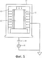
| JP2001023972A (ja) * | 1999-07-10 | 2001-01-26 | Nihon Ceratec Co Ltd | プラズマ処理装置 |
| EP1679532A1 (en) * | 2003-10-29 | 2006-07-12 | Matsushita Electric Industrial Co., Ltd. | Optical element having antireflection structure, and method for producing optical element having antireflection structure |
| JP2008256838A (ja) * | 2007-04-03 | 2008-10-23 | Canon Inc | レチクル及びレチクルの製造方法 |
Family Cites Families (9)
| Publication number | Priority date | Publication date | Assignee | Title |
|---|---|---|---|---|
| JPH11121901A (ja) * | 1997-08-11 | 1999-04-30 | Mitsui Chem Inc | 回路基板の製造方法 |
| JP4218372B2 (ja) * | 2003-03-06 | 2009-02-04 | コニカミノルタオプト株式会社 | 光学素子用金型の製造方法 |
| JP2004361635A (ja) * | 2003-06-04 | 2004-12-24 | Alps Electric Co Ltd | 曲面微細構造の形成方法 |
| US20070144700A1 (en) * | 2004-03-25 | 2007-06-28 | Sanyo Electric Co., Ltd. | Production method of curved-surface metal mold having fine uneven structure and production method of optical element using this metal mold |
| CN100458470C (zh) * | 2004-10-27 | 2009-02-04 | 株式会社尼康 | 光学元件制造方法、光学元件、尼普科夫盘、共焦光学系统以及三维测量装置 |
| KR100893251B1 (ko) * | 2004-12-03 | 2009-04-17 | 샤프 가부시키가이샤 | 반사 방지재, 광학 소자, 및 표시 장치 및 스탬퍼의 제조방법 및 스탬퍼를 이용한 반사 방지재의 제조 방법 |
| JP4539657B2 (ja) * | 2007-01-18 | 2010-09-08 | ソニー株式会社 | 反射防止用光学素子 |
| JP2008226340A (ja) * | 2007-03-12 | 2008-09-25 | Victor Co Of Japan Ltd | 光ディスク用原盤の製造方法及び光ディスク |
| JP4935513B2 (ja) * | 2007-06-06 | 2012-05-23 | ソニー株式会社 | 光学素子およびその製造方法、ならびに光学素子作製用複製基板およびその製造方法 |
-
2008
- 2008-12-26 JP JP2008335102A patent/JP4596072B2/ja not_active Expired - Fee Related
-
2009
- 2009-12-17 RU RU2010135583/28A patent/RU2457518C2/ru not_active IP Right Cessation
- 2009-12-17 CN CN200980108705.2A patent/CN102084272B/zh not_active Expired - Fee Related
- 2009-12-17 WO PCT/JP2009/071520 patent/WO2010074190A1/ja not_active Ceased
- 2009-12-17 US US12/919,666 patent/US20110249338A1/en not_active Abandoned
- 2009-12-17 KR KR1020107018855A patent/KR20110109809A/ko not_active Withdrawn
- 2009-12-23 TW TW098144568A patent/TWI425507B/zh not_active IP Right Cessation
Patent Citations (4)
| Publication number | Priority date | Publication date | Assignee | Title |
|---|---|---|---|---|
| JP2000121802A (ja) * | 1998-10-21 | 2000-04-28 | Alps Electric Co Ltd | 反射防止フィルムおよびその製造方法ならびに画像表示装置 |
| JP2001023972A (ja) * | 1999-07-10 | 2001-01-26 | Nihon Ceratec Co Ltd | プラズマ処理装置 |
| EP1679532A1 (en) * | 2003-10-29 | 2006-07-12 | Matsushita Electric Industrial Co., Ltd. | Optical element having antireflection structure, and method for producing optical element having antireflection structure |
| JP2008256838A (ja) * | 2007-04-03 | 2008-10-23 | Canon Inc | レチクル及びレチクルの製造方法 |
Also Published As
| Publication number | Publication date |
|---|---|
| TW201040959A (en) | 2010-11-16 |
| TWI425507B (zh) | 2014-02-01 |
| JP4596072B2 (ja) | 2010-12-08 |
| RU2010135583A (ru) | 2012-02-27 |
| WO2010074190A1 (ja) | 2010-07-01 |
| JP2010156843A (ja) | 2010-07-15 |
| CN102084272B (zh) | 2014-06-18 |
| KR20110109809A (ko) | 2011-10-06 |
| US20110249338A1 (en) | 2011-10-13 |
| CN102084272A (zh) | 2011-06-01 |
Similar Documents
| Publication | Publication Date | Title |
|---|---|---|
| RU2457518C2 (ru) | Элемент, полученный с помощью микрообработки, способ его изготовления и устройство травления | |
| CN102282482B (zh) | 光学元件、显示装置、抗反射光学部件和母片 | |
| RU2523764C2 (ru) | Антиотражающее оптическое устройство и способ изготовления эталонной формы | |
| JP5439783B2 (ja) | 光学素子、反射防止機能付き光学部品、および原盤 | |
| TWI387782B (zh) | 光學元件及其製造方法,形成光學元件之複製基板及其製造方法 | |
| CN102004272B (zh) | 光学器件及其制造方法和母板的制造方法 | |
| US20090135491A1 (en) | Optical element and method for manufacturing master for producing optical element | |
| JP2016105203A (ja) | 光学素子およびその製造方法、ならびに原盤の製造方法 | |
| JP2011002853A (ja) | 微細加工体の製造方法、およびエッチング装置 | |
| JP2015004993A (ja) | 光学素子およびその製造方法、ならびに原盤の製造方法 |
Legal Events
| Date | Code | Title | Description |
|---|---|---|---|
| MM4A | The patent is invalid due to non-payment of fees |
Effective date: 20151218 |