KR20180098372A - 금속 나노와이어층이 형성된 기재 및 그 제조 방법 - Google Patents
금속 나노와이어층이 형성된 기재 및 그 제조 방법 Download PDFInfo
- Publication number
- KR20180098372A KR20180098372A KR1020187021583A KR20187021583A KR20180098372A KR 20180098372 A KR20180098372 A KR 20180098372A KR 1020187021583 A KR1020187021583 A KR 1020187021583A KR 20187021583 A KR20187021583 A KR 20187021583A KR 20180098372 A KR20180098372 A KR 20180098372A
- Authority
- KR
- South Korea
- Prior art keywords
- substrate
- metal nanowire
- metal
- silver
- nanowire layer
- Prior art date
- Legal status (The legal status is an assumption and is not a legal conclusion. Google has not performed a legal analysis and makes no representation as to the accuracy of the status listed.)
- Ceased
Links
Images


Classifications
-
- B—PERFORMING OPERATIONS; TRANSPORTING
- B32—LAYERED PRODUCTS
- B32B—LAYERED PRODUCTS, i.e. PRODUCTS BUILT-UP OF STRATA OF FLAT OR NON-FLAT, e.g. CELLULAR OR HONEYCOMB, FORM
- B32B5/00—Layered products characterised by the non- homogeneity or physical structure, i.e. comprising a fibrous, filamentary, particulate or foam layer; Layered products characterised by having a layer differing constitutionally or physically in different parts
- B32B5/16—Layered products characterised by the non- homogeneity or physical structure, i.e. comprising a fibrous, filamentary, particulate or foam layer; Layered products characterised by having a layer differing constitutionally or physically in different parts characterised by features of a layer formed of particles, e.g. chips, powder or granules
-
- H—ELECTRICITY
- H01—ELECTRIC ELEMENTS
- H01B—CABLES; CONDUCTORS; INSULATORS; SELECTION OF MATERIALS FOR THEIR CONDUCTIVE, INSULATING OR DIELECTRIC PROPERTIES
- H01B5/00—Non-insulated conductors or conductive bodies characterised by their form
- H01B5/14—Non-insulated conductors or conductive bodies characterised by their form comprising conductive layers or films on insulating-supports
-
- B—PERFORMING OPERATIONS; TRANSPORTING
- B32—LAYERED PRODUCTS
- B32B—LAYERED PRODUCTS, i.e. PRODUCTS BUILT-UP OF STRATA OF FLAT OR NON-FLAT, e.g. CELLULAR OR HONEYCOMB, FORM
- B32B15/00—Layered products comprising a layer of metal
- B32B15/02—Layer formed of wires, e.g. mesh
-
- B—PERFORMING OPERATIONS; TRANSPORTING
- B32—LAYERED PRODUCTS
- B32B—LAYERED PRODUCTS, i.e. PRODUCTS BUILT-UP OF STRATA OF FLAT OR NON-FLAT, e.g. CELLULAR OR HONEYCOMB, FORM
- B32B15/00—Layered products comprising a layer of metal
- B32B15/04—Layered products comprising a layer of metal comprising metal as the main or only constituent of a layer, which is next to another layer of the same or of a different material
- B32B15/08—Layered products comprising a layer of metal comprising metal as the main or only constituent of a layer, which is next to another layer of the same or of a different material of synthetic resin
-
- B—PERFORMING OPERATIONS; TRANSPORTING
- B32—LAYERED PRODUCTS
- B32B—LAYERED PRODUCTS, i.e. PRODUCTS BUILT-UP OF STRATA OF FLAT OR NON-FLAT, e.g. CELLULAR OR HONEYCOMB, FORM
- B32B27/00—Layered products comprising a layer of synthetic resin
- B32B27/12—Layered products comprising a layer of synthetic resin next to a fibrous or filamentary layer
-
- B—PERFORMING OPERATIONS; TRANSPORTING
- B82—NANOTECHNOLOGY
- B82Y—SPECIFIC USES OR APPLICATIONS OF NANOSTRUCTURES; MEASUREMENT OR ANALYSIS OF NANOSTRUCTURES; MANUFACTURE OR TREATMENT OF NANOSTRUCTURES
- B82Y30/00—Nanotechnology for materials or surface science, e.g. nanocomposites
-
- B—PERFORMING OPERATIONS; TRANSPORTING
- B82—NANOTECHNOLOGY
- B82Y—SPECIFIC USES OR APPLICATIONS OF NANOSTRUCTURES; MEASUREMENT OR ANALYSIS OF NANOSTRUCTURES; MANUFACTURE OR TREATMENT OF NANOSTRUCTURES
- B82Y40/00—Manufacture or treatment of nanostructures
-
- H—ELECTRICITY
- H01—ELECTRIC ELEMENTS
- H01B—CABLES; CONDUCTORS; INSULATORS; SELECTION OF MATERIALS FOR THEIR CONDUCTIVE, INSULATING OR DIELECTRIC PROPERTIES
- H01B1/00—Conductors or conductive bodies characterised by the conductive materials; Selection of materials as conductors
- H01B1/02—Conductors or conductive bodies characterised by the conductive materials; Selection of materials as conductors mainly consisting of metals or alloys
- H01B1/026—Alloys based on copper
-
- H—ELECTRICITY
- H01—ELECTRIC ELEMENTS
- H01B—CABLES; CONDUCTORS; INSULATORS; SELECTION OF MATERIALS FOR THEIR CONDUCTIVE, INSULATING OR DIELECTRIC PROPERTIES
- H01B13/00—Apparatus or processes specially adapted for manufacturing conductors or cables
-
- H—ELECTRICITY
- H01—ELECTRIC ELEMENTS
- H01B—CABLES; CONDUCTORS; INSULATORS; SELECTION OF MATERIALS FOR THEIR CONDUCTIVE, INSULATING OR DIELECTRIC PROPERTIES
- H01B13/00—Apparatus or processes specially adapted for manufacturing conductors or cables
- H01B13/0026—Apparatus for manufacturing conducting or semi-conducting layers, e.g. deposition of metal
-
- H—ELECTRICITY
- H01—ELECTRIC ELEMENTS
- H01B—CABLES; CONDUCTORS; INSULATORS; SELECTION OF MATERIALS FOR THEIR CONDUCTIVE, INSULATING OR DIELECTRIC PROPERTIES
- H01B13/00—Apparatus or processes specially adapted for manufacturing conductors or cables
- H01B13/0036—Details
-
- H—ELECTRICITY
- H01—ELECTRIC ELEMENTS
- H01B—CABLES; CONDUCTORS; INSULATORS; SELECTION OF MATERIALS FOR THEIR CONDUCTIVE, INSULATING OR DIELECTRIC PROPERTIES
- H01B13/00—Apparatus or processes specially adapted for manufacturing conductors or cables
- H01B13/008—Apparatus or processes specially adapted for manufacturing conductors or cables for manufacturing extensible conductors or cables
Landscapes
- Engineering & Computer Science (AREA)
- Manufacturing & Machinery (AREA)
- Chemical & Material Sciences (AREA)
- Nanotechnology (AREA)
- Physics & Mathematics (AREA)
- Condensed Matter Physics & Semiconductors (AREA)
- General Physics & Mathematics (AREA)
- Crystallography & Structural Chemistry (AREA)
- Life Sciences & Earth Sciences (AREA)
- Wood Science & Technology (AREA)
- Composite Materials (AREA)
- Materials Engineering (AREA)
- Laminated Bodies (AREA)
- Chemically Coating (AREA)
- Non-Insulated Conductors (AREA)
- Manufacturing Of Electric Cables (AREA)
- Conductive Materials (AREA)
Abstract
Description
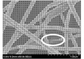
도 2는 실시예 1에 따른 무전해 니켈/금 도금 처리된 은 나노와이어/폴리우레탄 기재의 SEM 사진을 나타내는 도면이다.
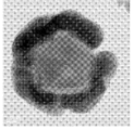
도 3은 실시예 1에 따른 무전해 니켈/금 도금 처리된 은 나노와이어의 단면 TEM 사진을 나타내는 도면이다.
도 4는 실시예 5에 따른 전해 백금 도금 처리된 은 나노와이어/폴리우레탄 기재의 SEM 사진을 나타내는 도면이다.
도 5는 실시예 5에 따른 전해 백금 도금 처리된 은 나노와이어의 단면 TEM 사진을 나타내는 도면이다.


Claims (9)
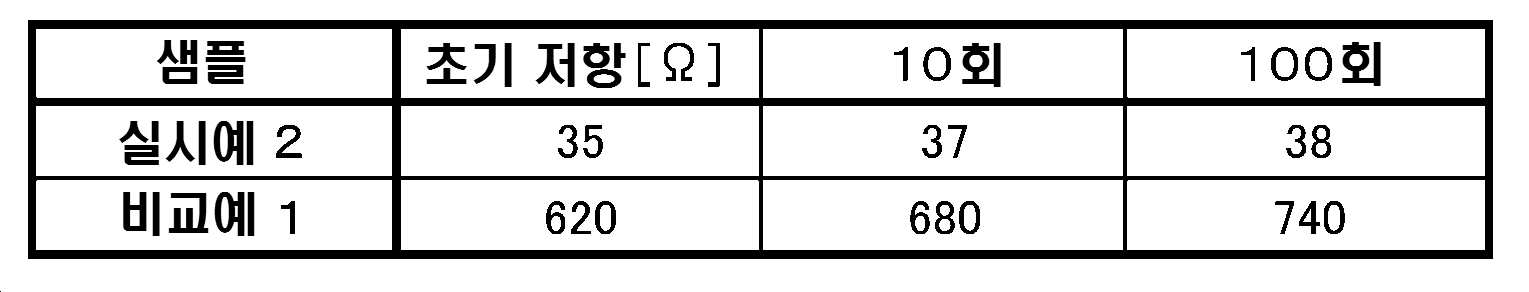
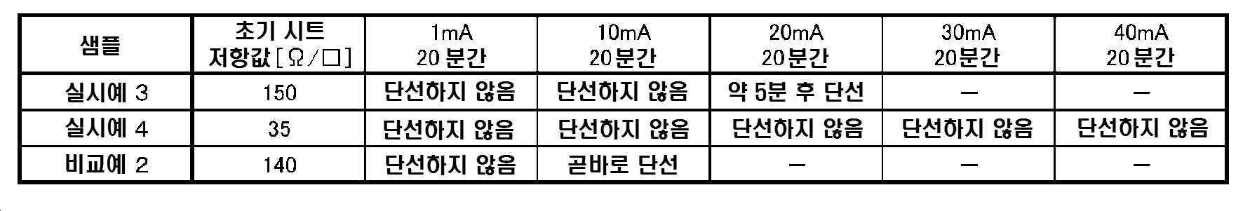
- 금속 나노와이어층이 형성된 기재로서, 금속 나노와이어의 일부가 기재에 매입된 상태이며, 노출되어 있는 금속 나노와이어의 일부 또는 전부가 도금되어 있는 것을 특징으로 하는 금속 나노와이어층이 형성된 기재.
- 제 1 항에 있어서,
상기 금속 나노와이어의 적어도 일부가 연결되어 있는 금속 나노와이어층이 형성된 기재. - 제 1 항 또는 제 2 항에 있어서,
상기 기재가 폴리우레탄, 실리콘 수지, 포화 폴리에스테르, 폴리카보네이트,폴리파라크실릴렌(파릴렌(등록상표)), 열가소성 폴리이미드, 폴리에테르술폰, 아크릴 수지, 폴리올레핀, 폴리염화비닐로 이루어지는 군 중 어느 하나인 금속 나노와이어층이 형성된 기재. - 제 1 항 내지 제 3 항 중 어느 한 항에 있어서,
상기 금속 나노와이어를 구성하는 금속이 은 또는 구리인 금속 나노와이어층이 형성된 기재. - 금속 나노와이어층을 기재 상에 형성하는 공정과, 상기 금속 나노와이어층이 형성된 기판에 외부 에너지를 부여하여 금속 나노와이어의 일부를 기재에 매입하는 공정과, 노출되어 있는 상기 금속 나노와이어의 일부 또는 전부를 도금하는 공정을 구비하는 것을 특징으로 하는 금속 나노와이어층이 형성된 기재의 제조 방법.
- 제 5 항에 있어서,
도금을 하는 공정의 전 또는 후에 상기 금속 나노와이어의 적어도 일부를 연결하는 공정을 더 포함하는 금속 나노와이어층이 형성된 기재의 제조 방법. - 제 5 항 또는 제 6 항에 있어서,
상기 기재가 폴리우레탄, 실리콘 수지, 포화 폴리에스테르, 폴리카보네이트,폴리파라크실릴렌(파릴렌(등록상표)), 열가소성 폴리이미드, 폴리에테르술폰, 아크릴 수지, 폴리올레핀, 폴리염화비닐로 이루어지는 군 중 어느 하나인 금속 나노와이어층이 형성된 기재의 제조 방법. - 제 5 항 내지 제 7 항 중 어느 한 항에 있어서,
상기 금속 나노와이어를 구성하는 금속이 은 또는 구리인 금속 나노와이어층이 형성된 기재의 제조 방법. - 제 1 항 내지 제 4 항 중 어느 한 항에 기재된 금속 나노와이어층이 형성된 기재를 구비한 센서 또는 기능 소자.
Applications Claiming Priority (3)
| Application Number | Priority Date | Filing Date | Title |
|---|---|---|---|
| JP2016055502 | 2016-03-18 | ||
| JPJP-P-2016-055502 | 2016-03-18 | ||
| PCT/JP2017/010264 WO2017159698A1 (ja) | 2016-03-18 | 2017-03-14 | 金属ナノワイヤ層が形成された基材及びその製造方法 |
Publications (1)
| Publication Number | Publication Date |
|---|---|
| KR20180098372A true KR20180098372A (ko) | 2018-09-03 |
Family
ID=59850328
Family Applications (1)
| Application Number | Title | Priority Date | Filing Date |
|---|---|---|---|
| KR1020187021583A Ceased KR20180098372A (ko) | 2016-03-18 | 2017-03-14 | 금속 나노와이어층이 형성된 기재 및 그 제조 방법 |
Country Status (5)
| Country | Link |
|---|---|
| JP (1) | JP6956706B2 (ko) |
| KR (1) | KR20180098372A (ko) |
| CN (1) | CN108604482A (ko) |
| TW (1) | TWI804462B (ko) |
| WO (1) | WO2017159698A1 (ko) |
Cited By (3)
| Publication number | Priority date | Publication date | Assignee | Title |
|---|---|---|---|---|
| KR20220026458A (ko) * | 2020-08-25 | 2022-03-04 | 티피케이 어드밴스트 솔루션스 인코포레이티드 | 터치 패널, 터치 패널의 제조 방법 및 그 디바이스 |
| KR20220026455A (ko) * | 2020-08-25 | 2022-03-04 | 티피케이 어드밴스트 솔루션스 인코포레이티드 | 터치 패널, 터치 패널의 제조 방법 및 그 디바이스 |
| US11347359B2 (en) | 2020-09-30 | 2022-05-31 | Tpk Advanced Solutions Inc. | Touch panel, manufacturing method of touch panel, and device thereof |
Families Citing this family (7)
| Publication number | Priority date | Publication date | Assignee | Title |
|---|---|---|---|---|
| JP7204195B2 (ja) * | 2018-01-26 | 2023-01-16 | ユニチカ株式会社 | めっき下地剤およびそれを用いた積層体 |
| CN108899279B (zh) * | 2018-06-30 | 2021-03-02 | 广州国显科技有限公司 | 纳米银线结构及其制备方法、显示面板 |
| CN110504068A (zh) * | 2019-08-11 | 2019-11-26 | 东北师范大学 | 一种高导电性及稳定性良好的透明银纳米线电极制备方法 |
| CN111333901B (zh) * | 2020-03-04 | 2022-09-20 | 上海海事大学 | 一种柔性复合材料及其制备与调控负介电性能的方法 |
| CN113744931A (zh) * | 2021-09-07 | 2021-12-03 | 浙江星隆新材料科技有限公司 | 一种图案化导电膜的制备方法 |
| CN116313237A (zh) * | 2023-03-24 | 2023-06-23 | 上海恩捷新材料科技有限公司 | 导电薄膜及其制备方法 |
| CN117219796B (zh) * | 2023-11-07 | 2024-02-13 | 武汉理工大学 | 一种Pt-Pd枝晶中空纳米线催化剂、其制备方法及应用 |
Citations (3)
| Publication number | Priority date | Publication date | Assignee | Title |
|---|---|---|---|---|
| WO2009035059A1 (ja) | 2007-09-12 | 2009-03-19 | Kuraray Co., Ltd. | 導電膜、導電部材および導電膜の製造方法 |
| JP2013151752A (ja) | 2013-03-01 | 2013-08-08 | Konica Minolta Inc | 金属ナノワイヤの製造方法 |
| WO2014175163A1 (ja) | 2013-04-26 | 2014-10-30 | 昭和電工株式会社 | 導電パターンの製造方法及び導電パターン形成基板 |
Family Cites Families (7)
| Publication number | Priority date | Publication date | Assignee | Title |
|---|---|---|---|---|
| JPH05151825A (ja) * | 1991-11-27 | 1993-06-18 | Sekisui Chem Co Ltd | 導電性透明体 |
| TWI426531B (zh) * | 2006-10-12 | 2014-02-11 | 坎畢歐科技公司 | 以奈米線為主之透明導體及其應用 |
| US20090321113A1 (en) * | 2007-04-20 | 2009-12-31 | Cambrios Technologies Corporation | High contrast transparent conductors and methods of forming the same |
| GB0908300D0 (en) * | 2009-05-14 | 2009-06-24 | Dupont Teijin Films Us Ltd | Polyester films |
| WO2011106438A1 (en) * | 2010-02-24 | 2011-09-01 | Cambrios Technologies Corporation | Nanowire-based transparent conductors and methods of patterning same |
| JP6700787B2 (ja) * | 2012-12-07 | 2020-05-27 | スリーエム イノベイティブ プロパティズ カンパニー | 基板上に透明導電体を製作する方法 |
| JP6022424B2 (ja) * | 2013-08-01 | 2016-11-09 | 日本写真印刷株式会社 | 透明導電性シート、および透明導電性シートを用いたタッチパネル |
-
2017
- 2017-03-14 JP JP2018505962A patent/JP6956706B2/ja active Active
- 2017-03-14 CN CN201780009177.XA patent/CN108604482A/zh active Pending
- 2017-03-14 KR KR1020187021583A patent/KR20180098372A/ko not_active Ceased
- 2017-03-14 WO PCT/JP2017/010264 patent/WO2017159698A1/ja not_active Ceased
- 2017-03-16 TW TW106108759A patent/TWI804462B/zh active
Patent Citations (3)
| Publication number | Priority date | Publication date | Assignee | Title |
|---|---|---|---|---|
| WO2009035059A1 (ja) | 2007-09-12 | 2009-03-19 | Kuraray Co., Ltd. | 導電膜、導電部材および導電膜の製造方法 |
| JP2013151752A (ja) | 2013-03-01 | 2013-08-08 | Konica Minolta Inc | 金属ナノワイヤの製造方法 |
| WO2014175163A1 (ja) | 2013-04-26 | 2014-10-30 | 昭和電工株式会社 | 導電パターンの製造方法及び導電パターン形成基板 |
Cited By (3)
| Publication number | Priority date | Publication date | Assignee | Title |
|---|---|---|---|---|
| KR20220026458A (ko) * | 2020-08-25 | 2022-03-04 | 티피케이 어드밴스트 솔루션스 인코포레이티드 | 터치 패널, 터치 패널의 제조 방법 및 그 디바이스 |
| KR20220026455A (ko) * | 2020-08-25 | 2022-03-04 | 티피케이 어드밴스트 솔루션스 인코포레이티드 | 터치 패널, 터치 패널의 제조 방법 및 그 디바이스 |
| US11347359B2 (en) | 2020-09-30 | 2022-05-31 | Tpk Advanced Solutions Inc. | Touch panel, manufacturing method of touch panel, and device thereof |
Also Published As
| Publication number | Publication date |
|---|---|
| JPWO2017159698A1 (ja) | 2019-01-24 |
| CN108604482A (zh) | 2018-09-28 |
| WO2017159698A1 (ja) | 2017-09-21 |
| TWI804462B (zh) | 2023-06-11 |
| JP6956706B2 (ja) | 2021-11-02 |
| TW201801901A (zh) | 2018-01-16 |
Similar Documents
| Publication | Publication Date | Title |
|---|---|---|
| KR20180098372A (ko) | 금속 나노와이어층이 형성된 기재 및 그 제조 방법 | |
| US12336115B2 (en) | Liquid metal fusion with conductive inks and pastes | |
| An et al. | Self-Junctioned Copper Nanofiber Transparent Flexible Conducting Film via Electrospinning and Electroplating. | |
| Zhang et al. | Conformal manufacturing of soft deformable sensors on the curved surface | |
| KR20160014703A (ko) | 투명 전극 및 그 제조 방법 | |
| CN108701505A (zh) | 伸缩性导体片、具有粘接性的伸缩性导体片、布帛上的伸缩性导体构成的配线的形成方法 | |
| JP7028564B2 (ja) | 可とう性配線基板または可とう性導電体構造物、その製造方法、およびこれを含む電子素子 | |
| CN113630915A (zh) | 灵活定制高可调柔性微加热器的复合加工方法及微加热器 | |
| Zhang et al. | Hierarchically Oriented Jellyfish‐Like Gold Nanowires Film for Elastronics | |
| KR20200041799A (ko) | 전도성 섬유 및 제조방법 | |
| Abdulrhman et al. | Routes towards manufacturing biodegradable electronics with polycaprolactone (PCL) via direct light writing and electroless plating | |
| CN107610815A (zh) | 一种银纳米线透明复合涂层及其制备方法 | |
| JP7837987B2 (ja) | 付加製造システム、付加製造システムを形成する方法、および複合構造を形成する方法 | |
| JP5967778B2 (ja) | 導電性ポリマー−金属複合体の析出方法、導電性ポリマー−金属複合体、フレキシブル基板上への導電配線パターン形成方法、及びフレキシブル基板 | |
| Xie et al. | A facile and universally applicable additive strategy for fabrication of high-quality copper patterns based on a homogeneous Ag catalyst ink | |
| KR20090126825A (ko) | 코어쉘 나노선 및 그 제조 방법 | |
| TWI552171B (zh) | 導電薄膜及其製備方法 | |
| KR101221980B1 (ko) | 납땜이 가능한 플렉서블 전극 및 그 제조방법 | |
| JP6542572B2 (ja) | 伸縮性導電フィルムおよび伸縮性導電フィルムの製造方法 | |
| Zhou et al. | Chemically activated Ag-embedded bridged-layer for copper pattern addition on PET film | |
| KR102439113B1 (ko) | 실리카 크랙을 통한 네트워크형 나노 금속층이 도금된 복합소재의 제조방법 및 그로부터 제조된 웨어러블 일렉트로닉스 탄소섬유 | |
| JP2008027636A (ja) | 透明導電膜の製造方法 | |
| CN116655977B (zh) | 基于可靠界面结合的柔性多功能薄膜的制备方法及器件 | |
| RU2770237C1 (ru) | Устройство приёмопередающее и способ его изготовления | |
| TWI620834B (zh) | 可撓式發光裝置及其製造方法 |
Legal Events
| Date | Code | Title | Description |
|---|---|---|---|
| A201 | Request for examination | ||
| AMND | Amendment | ||
| PA0105 | International application |
Patent event date: 20180726 Patent event code: PA01051R01D Comment text: International Patent Application |
|
| PA0201 | Request for examination | ||
| PG1501 | Laying open of application | ||
| E902 | Notification of reason for refusal | ||
| PE0902 | Notice of grounds for rejection |
Comment text: Notification of reason for refusal Patent event date: 20191121 Patent event code: PE09021S01D |
|
| AMND | Amendment | ||
| E601 | Decision to refuse application | ||
| PE0601 | Decision on rejection of patent |
Patent event date: 20200526 Comment text: Decision to Refuse Application Patent event code: PE06012S01D Patent event date: 20191121 Comment text: Notification of reason for refusal Patent event code: PE06011S01I |
|
| X091 | Application refused [patent] | ||
| AMND | Amendment | ||
| PX0901 | Re-examination |
Patent event code: PX09011S01I Patent event date: 20200526 Comment text: Decision to Refuse Application Patent event code: PX09012R01I Patent event date: 20200121 Comment text: Amendment to Specification, etc. Patent event code: PX09012R01I Patent event date: 20180726 Comment text: Amendment to Specification, etc. |
|
| PX0601 | Decision of rejection after re-examination |
Comment text: Decision to Refuse Application Patent event code: PX06014S01D Patent event date: 20200721 Comment text: Amendment to Specification, etc. Patent event code: PX06012R01I Patent event date: 20200625 Comment text: Decision to Refuse Application Patent event code: PX06011S01I Patent event date: 20200526 Comment text: Amendment to Specification, etc. Patent event code: PX06012R01I Patent event date: 20200121 Comment text: Notification of reason for refusal Patent event code: PX06013S01I Patent event date: 20191121 Comment text: Amendment to Specification, etc. Patent event code: PX06012R01I Patent event date: 20180726 |
|
| X601 | Decision of rejection after re-examination |