KR20180098372A - Substrate having metal nanowire layer formed thereon and method for manufacturing the same - Google Patents
Substrate having metal nanowire layer formed thereon and method for manufacturing the same Download PDFInfo
- Publication number
- KR20180098372A KR20180098372A KR1020187021583A KR20187021583A KR20180098372A KR 20180098372 A KR20180098372 A KR 20180098372A KR 1020187021583 A KR1020187021583 A KR 1020187021583A KR 20187021583 A KR20187021583 A KR 20187021583A KR 20180098372 A KR20180098372 A KR 20180098372A
- Authority
- KR
- South Korea
- Prior art keywords
- substrate
- metal nanowire
- metal
- silver
- nanowire layer
- Prior art date
- Legal status (The legal status is an assumption and is not a legal conclusion. Google has not performed a legal analysis and makes no representation as to the accuracy of the status listed.)
- Ceased
Links
Images


Classifications
-
- B—PERFORMING OPERATIONS; TRANSPORTING
- B32—LAYERED PRODUCTS
- B32B—LAYERED PRODUCTS, i.e. PRODUCTS BUILT-UP OF STRATA OF FLAT OR NON-FLAT, e.g. CELLULAR OR HONEYCOMB, FORM
- B32B5/00—Layered products characterised by the non- homogeneity or physical structure, i.e. comprising a fibrous, filamentary, particulate or foam layer; Layered products characterised by having a layer differing constitutionally or physically in different parts
- B32B5/16—Layered products characterised by the non- homogeneity or physical structure, i.e. comprising a fibrous, filamentary, particulate or foam layer; Layered products characterised by having a layer differing constitutionally or physically in different parts characterised by features of a layer formed of particles, e.g. chips, powder or granules
-
- H—ELECTRICITY
- H01—ELECTRIC ELEMENTS
- H01B—CABLES; CONDUCTORS; INSULATORS; SELECTION OF MATERIALS FOR THEIR CONDUCTIVE, INSULATING OR DIELECTRIC PROPERTIES
- H01B5/00—Non-insulated conductors or conductive bodies characterised by their form
- H01B5/14—Non-insulated conductors or conductive bodies characterised by their form comprising conductive layers or films on insulating-supports
-
- B—PERFORMING OPERATIONS; TRANSPORTING
- B32—LAYERED PRODUCTS
- B32B—LAYERED PRODUCTS, i.e. PRODUCTS BUILT-UP OF STRATA OF FLAT OR NON-FLAT, e.g. CELLULAR OR HONEYCOMB, FORM
- B32B15/00—Layered products comprising a layer of metal
- B32B15/02—Layer formed of wires, e.g. mesh
-
- B—PERFORMING OPERATIONS; TRANSPORTING
- B32—LAYERED PRODUCTS
- B32B—LAYERED PRODUCTS, i.e. PRODUCTS BUILT-UP OF STRATA OF FLAT OR NON-FLAT, e.g. CELLULAR OR HONEYCOMB, FORM
- B32B15/00—Layered products comprising a layer of metal
- B32B15/04—Layered products comprising a layer of metal comprising metal as the main or only constituent of a layer, which is next to another layer of the same or of a different material
- B32B15/08—Layered products comprising a layer of metal comprising metal as the main or only constituent of a layer, which is next to another layer of the same or of a different material of synthetic resin
-
- B—PERFORMING OPERATIONS; TRANSPORTING
- B32—LAYERED PRODUCTS
- B32B—LAYERED PRODUCTS, i.e. PRODUCTS BUILT-UP OF STRATA OF FLAT OR NON-FLAT, e.g. CELLULAR OR HONEYCOMB, FORM
- B32B27/00—Layered products comprising a layer of synthetic resin
- B32B27/12—Layered products comprising a layer of synthetic resin next to a fibrous or filamentary layer
-
- B—PERFORMING OPERATIONS; TRANSPORTING
- B82—NANOTECHNOLOGY
- B82Y—SPECIFIC USES OR APPLICATIONS OF NANOSTRUCTURES; MEASUREMENT OR ANALYSIS OF NANOSTRUCTURES; MANUFACTURE OR TREATMENT OF NANOSTRUCTURES
- B82Y30/00—Nanotechnology for materials or surface science, e.g. nanocomposites
-
- B—PERFORMING OPERATIONS; TRANSPORTING
- B82—NANOTECHNOLOGY
- B82Y—SPECIFIC USES OR APPLICATIONS OF NANOSTRUCTURES; MEASUREMENT OR ANALYSIS OF NANOSTRUCTURES; MANUFACTURE OR TREATMENT OF NANOSTRUCTURES
- B82Y40/00—Manufacture or treatment of nanostructures
-
- H—ELECTRICITY
- H01—ELECTRIC ELEMENTS
- H01B—CABLES; CONDUCTORS; INSULATORS; SELECTION OF MATERIALS FOR THEIR CONDUCTIVE, INSULATING OR DIELECTRIC PROPERTIES
- H01B1/00—Conductors or conductive bodies characterised by the conductive materials; Selection of materials as conductors
- H01B1/02—Conductors or conductive bodies characterised by the conductive materials; Selection of materials as conductors mainly consisting of metals or alloys
- H01B1/026—Alloys based on copper
-
- H—ELECTRICITY
- H01—ELECTRIC ELEMENTS
- H01B—CABLES; CONDUCTORS; INSULATORS; SELECTION OF MATERIALS FOR THEIR CONDUCTIVE, INSULATING OR DIELECTRIC PROPERTIES
- H01B13/00—Apparatus or processes specially adapted for manufacturing conductors or cables
-
- H—ELECTRICITY
- H01—ELECTRIC ELEMENTS
- H01B—CABLES; CONDUCTORS; INSULATORS; SELECTION OF MATERIALS FOR THEIR CONDUCTIVE, INSULATING OR DIELECTRIC PROPERTIES
- H01B13/00—Apparatus or processes specially adapted for manufacturing conductors or cables
- H01B13/0026—Apparatus for manufacturing conducting or semi-conducting layers, e.g. deposition of metal
-
- H—ELECTRICITY
- H01—ELECTRIC ELEMENTS
- H01B—CABLES; CONDUCTORS; INSULATORS; SELECTION OF MATERIALS FOR THEIR CONDUCTIVE, INSULATING OR DIELECTRIC PROPERTIES
- H01B13/00—Apparatus or processes specially adapted for manufacturing conductors or cables
- H01B13/0036—Details
-
- H—ELECTRICITY
- H01—ELECTRIC ELEMENTS
- H01B—CABLES; CONDUCTORS; INSULATORS; SELECTION OF MATERIALS FOR THEIR CONDUCTIVE, INSULATING OR DIELECTRIC PROPERTIES
- H01B13/00—Apparatus or processes specially adapted for manufacturing conductors or cables
- H01B13/008—Apparatus or processes specially adapted for manufacturing conductors or cables for manufacturing extensible conductors or cables
Landscapes
- Engineering & Computer Science (AREA)
- Manufacturing & Machinery (AREA)
- Chemical & Material Sciences (AREA)
- Nanotechnology (AREA)
- Physics & Mathematics (AREA)
- Condensed Matter Physics & Semiconductors (AREA)
- General Physics & Mathematics (AREA)
- Crystallography & Structural Chemistry (AREA)
- Life Sciences & Earth Sciences (AREA)
- Wood Science & Technology (AREA)
- Composite Materials (AREA)
- Materials Engineering (AREA)
- Laminated Bodies (AREA)
- Chemically Coating (AREA)
- Non-Insulated Conductors (AREA)
- Manufacturing Of Electric Cables (AREA)
- Conductive Materials (AREA)
Abstract
마이그레이션 및 황화·산화 등에 대해 높은 내구성을 가짐과 아울러 높은 기계적 강도를 갖는 금속 나노와이어층이 형성된 기판으로서, 금속 나노와이어층을 기재 상에 형성하고, 외부 에너지를 부여함으로써 금속 나노와이어의 일부가 가요 성을 갖는 기재에 매입된 상태이며, 노출되어 있는 금속 나노와이어의 일부 또는 전부가 도금되어 있는 금속 나노와이어층이 형성된 기재.Migration, sulphidation, oxidation, and the like, and a metal nanowire layer having high mechanical strength is formed, a part of the metal nanowire is formed by forming a metal nanowire layer on a substrate and applying external energy And a metal nanowire layer in which a part or all of the exposed metal nanowires are plated is formed.

Description
본 발명은 금속 나노와이어층이 형성된 기재 및 그 제조 방법에 관한 것이다. The present invention relates to a substrate on which a metal nanowire layer is formed and a manufacturing method thereof.
금속 나노와이어는 종래의 ITO로 대표되는 투명 도전막 재료에 비해 투명성이나 도전성이 우수한 투명 도전체를 형성할 수 있는 재료일 뿐만 아니라, 굽힘이나 신축 등의 기계적 내구성이 우수하기 때문에 가요성을 갖는 필름 기재 등을 이용한 투명 도전막의 형성 등에 사용되고 있다. 예를 들면, 하기 특허문헌 1에는 금속 나노와이어를 사용한 도전 패턴의 제조 방법이 개시되어 있다. The metal nanowire is not only a material capable of forming a transparent conductor having excellent transparency and conductivity as compared with a transparent conductive film material typified by conventional ITO but also has excellent mechanical durability such as bending and elongation and shrinkage, Forming a transparent conductive film using a substrate or the like. For example, Patent Document 1 below discloses a method of manufacturing a conductive pattern using metal nanowires.
그러나, 은이나 구리 등으로 제작되는 금속 나노와이어를 투명 도전막 재료로 이용한 경우, 마이그레이션이나 황화·산화 등에 의해 투명 도전막의 열화가 진행하는 경우가 있다. 그래서, 금속 나노와이어의 내구성 향상을 도모하기 위해 그래핀이나 폴리머를 투명 도전막의 전면에 코팅할 수 있는 것이 행해져 왔지만, 높은 내구성의 확보에는 이르러 있지 않다. However, when a metal nanowire made of silver, copper, or the like is used as a transparent conductive film material, deterioration of the transparent conductive film sometimes proceeds due to migration, sulphation, oxidation, or the like. Thus, in order to improve the durability of the metal nanowires, graphene or a polymer can be coated on the entire surface of the transparent conductive film, but high durability has not yet been secured.
최근, 은 나노와이어에 도금을 실시하여 내구성을 향상시키는 기술이 제안되어 있다. 예를 들면, 하기 특허문헌 2에는 은 나노와이어의 표면에 은 이외의 금속을 도금한 구성이 개시되어 있다. Recently, a technique has been proposed in which silver nanowires are plated to improve durability. For example, Patent Document 2 below discloses a configuration in which a surface of a silver nanowire is plated with a metal other than silver.
또한, 하기 특허문헌 3에는 직선 형상 금속 나노와이어가 서로 교점에서 접합하여 그물코를 형성하고 있는 도전막에 있어서, 상기 접합이 압착 또는 도금에 의해 되어 있는 점이 기재되어 있다. Further, in Patent Document 3, it is described that, in a conductive film in which straight-line metal nanowires are joined at their intersecting points to form a mesh, the bonding is performed by pressing or plating.
그러나, 상기 종래 기술에 있어서의 도금 기술에서는 금속 나노와이어가 기판으로부터 용이하게 박리되어 안정된 도금 처리를 행할 수 없다. 또한, 금속 나노와이어로 구성된 투명 도전막을 단지 기판 상에 형성한 것만으로는 굽힘이나 신축에 대한 높은 기계적 강도를 얻을 수 없다. However, in the above-described plating technique in the conventional technique, the metal nanowires are easily peeled off from the substrate and the stable plating process can not be performed. In addition, high mechanical strength against bending and elongation can not be obtained by simply forming a transparent conductive film composed of metal nanowires on a substrate.
본 발명의 목적은 마이그레이션이나 황화·산화 등에 대하여 높은 내구성을 가짐과 아울러 높은 기계적 강도를 갖는 금속 나노와이어층이 형성된 기재 및 그 제조 방법을 제공하는 것에 있다. An object of the present invention is to provide a substrate having a metal nanowire layer having high durability against migration, sulfidation, oxidation, etc., and having high mechanical strength, and a method for producing the same.
상기 목적을 달성하기 위하여, 본 발명은 이하의 실시형태를 갖는다. In order to achieve the above object, the present invention has the following embodiments.
[1] 금속 나노와이어층이 형성된 기재로서, 금속 나노와이어의 일부가 기재에 매입된 상태이며, 노출되어 있는 금속 나노와이어의 일부 또는 전부가 도금되어 있는 것을 특징으로 하는 금속 나노와이어층이 형성된 기재. [1] A substrate on which a metal nanowire layer is formed, wherein a part of the metal nanowire is embedded in the substrate, and a part or all of the exposed metal nanowire is plated. .
[2] [1]에 있어서,[2] The method according to [1]
상기 금속 나노와이어의 적어도 일부가 연결되어 있는 금속 나노와이어층이 형성된 기재. And a metal nanowire layer having at least a part of the metal nanowires connected thereto.
[3] [1] 또는 [2]에 있어서,[3] The method according to [1] or [2]
상기 기재가 폴리우레탄, 실리콘 수지, 포화 폴리에스테르, 폴리카보네이트,폴리파라크실릴렌(파릴렌(등록상표)), 열가소성 폴리이미드, 폴리에테르술폰, 아크릴 수지, 폴리올레핀, 폴리염화비닐로 이루어지는 군 중 어느 하나인 금속 나노와이어층이 형성된 기재. Wherein the substrate is selected from the group consisting of polyurethane, silicone resin, saturated polyester, polycarbonate, polyparaxylylene (parylene (registered trademark)), thermoplastic polyimide, polyether sulfone, acrylic resin, polyolefin, A substrate on which a metal nanowire layer is formed.
[4] [1] 내지 [3] 중 어느 하나에 있어서,[4] The method according to any one of [1] to [3]
상기 금속 나노와이어를 구성하는 금속이 은 또는 구리인 금속 나노와이어층이 형성된 기재. And a metal nanowire layer in which the metal constituting the metal nanowire is silver or copper.
[5] 금속 나노와이어층을 기재 상에 형성하는 공정과, 상기 금속 나노와이어층이 형성된 기판에 외부 에너지를 부여하여 금속 나노와이어의 일부를 기재에 매입하는 공정과, 노출되어 있는 상기 금속 나노와이어의 일부 또는 전부를 도금하는 공정을 구비하는 것을 특징으로 하는 금속 나노와이어층이 형성된 기재의 제조 방법. A step of forming a metal nanowire layer on a substrate; a step of applying external energy to the substrate on which the metal nanowire layer is formed to embed a part of the metal nanowire in the substrate; And a step of plating a part or the whole of the metal nanowire layer.
[6] [5]에 있어서,[6] The method according to [5]
도금을 하는 공정의 전 또는 후에 상기 금속 나노와이어의 적어도 일부를 연결하는 공정을 더 포함하는 금속 나노와이어층이 형성된 기재의 제조 방법. And a step of connecting at least a part of the metal nanowires before or after the step of plating the metal nanowires.
[7] [5] 또는 [6]에 있어서,[7] The method according to [5] or [6]
상기 기재가 폴리우레탄, 실리콘 수지, 포화 폴리에스테르, 폴리카보네이트,폴리파라크실릴렌(파릴렌(등록상표)), 열가소성 폴리이미드, 폴리에테르술폰, 아크릴 수지, 폴리올레핀, 폴리염화비닐로 이루어지는 군 중 어느 하나인 금속 나노와이어층이 형성된 기재의 제조 방법. Wherein the substrate is selected from the group consisting of polyurethane, silicone resin, saturated polyester, polycarbonate, polyparaxylylene (parylene (registered trademark)), thermoplastic polyimide, polyether sulfone, acrylic resin, polyolefin, Wherein a metal nanowire layer is formed on the substrate.
[8] [5] 내지 [7] 중 어느 하나에 있어서,[8] The method according to any one of [5] to [7]
상기 금속 나노와이어를 구성하는 금속이 은 또는 구리인 금속 나노와이어층이 형성된 기재의 제조 방법. Wherein a metal nanowire layer of which the metal constituting the metal nanowire is silver or copper is formed.
[9] 상기 [1] 내지 [4] 중 어느 하나에 기재된 금속 나노와이어층이 형성된 기재를 구비한 센서 또는 기능 소자.[9] A sensor or a functional device comprising the substrate on which the metal nanowire layer according to any one of [1] to [4] is formed.
(발명의 효과)(Effects of the Invention)
본 발명에 의하면, 마이그레이션이나 황화·산화 등에 대하여 높은 내구성을 가짐과 아울러 높은 기계적 강도를 갖는 금속 나노와이어층이 형성된 기재 및 그 제조 방법을 제공할 수 있다. According to the present invention, it is possible to provide a base material having a metal nanowire layer having high durability against migration, sulfidation, oxidation, etc., and having high mechanical strength, and a method for producing the same.
도 1은 실시형태에 따른 금속 나노와이어층이 형성된 기재의 제조 공정예의 설명도이다.
도 2는 실시예 1에 따른 무전해 니켈/금 도금 처리된 은 나노와이어/폴리우레탄 기재의 SEM 사진을 나타내는 도면이다.
도 3은 실시예 1에 따른 무전해 니켈/금 도금 처리된 은 나노와이어의 단면 TEM 사진을 나타내는 도면이다.
도 4는 실시예 5에 따른 전해 백금 도금 처리된 은 나노와이어/폴리우레탄 기재의 SEM 사진을 나타내는 도면이다.
도 5는 실시예 5에 따른 전해 백금 도금 처리된 은 나노와이어의 단면 TEM 사진을 나타내는 도면이다. BRIEF DESCRIPTION OF THE DRAWINGS FIG. 1 is an explanatory diagram of an example of a production process of a substrate on which a metal nanowire layer is formed according to the embodiment;
FIG. 2 is a SEM photograph of a silver nanowire / polyurethane base treated with electroless nickel / gold plating according to Example 1. FIG.
FIG. 3 is a cross-sectional TEM photograph of the electroless nickel / gold-plated silver nanowire according to Example 1. FIG.
4 is a SEM photograph of a silver nanowire / polyurethane substrate treated with electrolytic platinum according to Example 5. FIG.
5 is a cross-sectional TEM photograph of the silver nanowire treated with electrolytic platinum according to Example 5. FIG.
이하, 본 발명을 실시하기 위한 형태(이하, 실시형태라고 한다)를 설명한다. Hereinafter, a mode for carrying out the present invention (hereinafter referred to as an embodiment) will be described.
실시형태에 따른 금속 나노와이어층이 형성된 기재는 금속 나노와이어의 일부가 기재에 매입된 상태이며, 노출되어 있는 금속 나노와이어의 일부 또는 전부가 도금되어 있는 것을 특징으로 한다. The substrate on which the metal nanowire layer is formed according to the embodiment is characterized in that a part of the metal nanowire is embedded in the substrate and a part or all of the exposed metal nanowires are plated.
상기 금속 나노와이어는 지름이 나노미터 오더의 크기인 금속이며, 와이어 형상의 형상을 갖는 도전성 재료이다. 또한, 본 실시형태에서는 금속 나노와이어와 함께(혼합하여), 또는 금속 나노와이어 대신에 다공질 또는 비다공질의 튜브 형상의 형상을 갖는 도전성 재료인 금속 나노튜브를 사용해도 좋다. 본 명세서에 있어서, 「와이어 형상」과 「튜브 형상」은 모두 선 형상이지만, 전자는 중앙이 중공이 아닌 것, 후자는 중앙이 중공인 것을 의도한다. 성상은 유연해도 좋고 강직이어도 좋다. 이하, 본원 명세서에 있어서 「금속 나노와이어」와 「금속 나노튜브」를 계속해서 표기하지 않는 경우, 「금속 나노와이어」는 금속 나노와이어와 금속 나노튜브를 포괄하는 의미로 사용한다. The metal nanowire is a metal having a diameter on the order of nanometers and is a conductive material having a wire-like shape. In this embodiment mode, a metal nanotube, which is a conductive material having a porous or non-porous tube shape instead of the metal nanowire, may be used (mixed) together with the metal nanowire. In the present specification, the terms "wire shape" and "tube shape" are both linear, but the former is intended to be hollow at the center and the latter to hollow at the center. The property may be flexible or rigid. Hereinafter, in the present specification, when "metal nanowires" and "metal nanotubes" are not continuously described, "metal nanowires" are used to mean metal nanowires and metal nanotubes.
금속 나노와이어 또는 금속 나노튜브의 제조 방법으로서는 공지의 제조 방법을 사용할 수 있다. 예를 들면, 은 나노와이어는 폴리올(Poly-ol)법을 이용하여 폴리비닐피롤리돈 존재 하에서 질산은을 환원함으로써 합성할 수 있다(Chem. Mater., 2002, 14, 4736 참조). 금 나노와이어도 마찬가지로 폴리비닐피롤리돈 존재 하에서 염화금산 수화물을 환원함으로써 합성할 수 있다(J.Am.Chem.Soc., 2007, 129, 1733 참조). 은 나노와이어 및 금 나노와이어의 대규모의 합성 및 정제의 기술에 관해서는 국제 공개 제2008/073143호 팜플렛과 국제 공개 제2008/046058호 팜플렛에 상세한 기술이 있다. 다공질 구조를 갖는 금 나노튜브는 은 나노와이어를 주형으로 하여 염화금산 용액을 환원함으로써 합성할 수 있다. 여기서, 주형으로 이용한 은 나노와이어는 염화금산과의 산화 환원 반응에 의해 용액 중에 용출하여, 결과로서 다공질 구조를 갖는 금 나노튜브가 생긴다(J. Am. Chem. Soc., 2004, 126, 3892-3901 참조). As a method for producing the metal nanowire or the metal nanotube, a known manufacturing method can be used. For example, silver nanowires can be synthesized by reducing silver nitrate in the presence of polyvinyl pyrrolidone using the poly-ol method (see Chem. Mater. 2002, 14, 4736). Gold nanowires can also be synthesized by reducing chloroauric acid hydrate in the presence of polyvinylpyrrolidone (see J. Am. Chem. Soc., 2007, 129, 1733). There is a detailed description of the technology of large scale synthesis and purification of silver nanowires and gold nanowires in WO 2008/073143 and International Publication WO 2008/046058 pamphlet. A gold nanotube having a porous structure can be synthesized by reducing a chloroauric acid solution using silver nanowire as a template. Here, silver nanowires used as a template are eluted into a solution by redox reaction with chloroauric acid, resulting in gold nanotubes having a porous structure (J. Am. Chem. Soc., 2004, 126, 3892- 3901).
금속 나노와이어 및 금속 나노튜브의 지름의 두께의 평균은 1~500㎚가 바람직하고, 5~200㎚가 보다 바람직하고, 5~100㎚가 더욱 바람직하고, 10~100㎚가 특히 바람직하다. 또한, 금속 나노와이어 및 금속 나노튜브의 장축의 길이의 평균은 1~100㎛가 바람직하고, 1~80㎛가 보다 바람직하고, 2~70㎛가 더욱 바람직하고, 5~50㎛가 특히 바람직하다. 금속 나노와이어 및 금속 나노튜브는 지름의 두께의 평균 및 장축의 길이의 평균이 상기 범위를 충족함과 아울러 아스펙트비의 평균이 5보다 큰 것이 바람직하고, 10 이상인 것이 보다 바람직하고, 100 이상인 것이 더욱 바람직하고, 200 이상인 것이 특히 바람직하다. 여기서, 아스펙트비는 금속 나노와이어 및 금속 나노튜브의 지름의 평균 지름을 b, 장축의 평균적인 길이를 a로 근사한 경우, a/b로 구해지는 값이다. a 및 b는 주사형 전자 현미경(SEM) 및 광학 현미경을 이용하여 측정할 수 있다. 구체적으로는, 금속 나노와이어의 10개 이상의 지름을 SEM(히타치하이테크놀로지스사제 FE-SEM SU8020)에 의해 각각 측장, 금속 나노와이어의 100개 이상의 길이를 광학 현미경(키엔스사제 VHX-600)을 이용하여 각각 측장하여, 그것들의 상가 평균값에 의해 평균 지름 및 평균 길이를 구할 수 있다. The average diameter of the thickness of the metal nanowires and the metal nanotubes is preferably 1 to 500 nm, more preferably 5 to 200 nm, still more preferably 5 to 100 nm, particularly preferably 10 to 100 nm. The average length of the long axes of the metal nanowires and the metal nanotubes is preferably 1 to 100 占 퐉, more preferably 1 to 80 占 퐉, still more preferably 2 to 70 占 퐉, and particularly preferably 5 to 50 占 퐉 . The metal nanowires and the metal nanotubes preferably have an average of the average diameter and the length of the major axis of the diameter and a mean aspect ratio of more than 5, more preferably 10 or more, and more preferably 100 or more More preferably 200 or more. Here, the aspect ratio is a value obtained by a / b when the average diameter of the metal nanowires and metal nanotubes is b and the average length of the major axis is a. a and b can be measured using a scanning electron microscope (SEM) and an optical microscope. More specifically, a diameter of 10 or more of the metal nanowires was measured by SEM (FE-SEM SU8020, manufactured by Hitachi High Technologies), respectively, and lengths of 100 or more of the metal nanowires were measured with an optical microscope (VHX-600, And the average diameter and the average length can be obtained from the average values of the images.
이러한 금속 나노와이어의 재료로서는 재료 자체가 마이그레이션이나 황화·산화 등에 대한 내구성에 다소 어려움이 있어 향상이 요구되는 재료라면 특별히 제한은 없지만 도전성이 높은 점에서 은, 구리 등이 적합하다. The material of the metal nanowire is not particularly limited as long as the material itself is somewhat difficult to durability against migration, sulphidation, oxidation and the like and is required to be improved. However, silver is preferable from the viewpoint of high conductivity.
또한, 상기 기재는 열가소성 수지 재료인 것이 바람직하다. 열가소성 수지는 착색되어 있어도 좋지만, 가시광에 의한 투명성은 높은 쪽이 바람직하다. 예를 들면, 폴리우레탄, 실리콘 수지, 포화 폴리에스테르(폴리에틸렌테레프탈레이트(PET), 폴리에틸렌나프탈레이트(PEN) 등), 폴리카보네이트, 폴리파라크실릴렌(파릴렌(등록상표)), 열가소성 폴리이미드, 폴리에테르술폰, 아크릴 수지, 폴리올레핀, 폴리염화비닐 등이 예시된다. 이들 중에서도, 금속 나노와이어의 기재와의 밀착성이나 기재의 신축성의 관점에서 폴리우레탄, 폴리에틸렌테레프탈레이트(PET), 폴리파라크실릴렌(파릴렌(R))이 바람직하다. The base material is preferably a thermoplastic resin material. The thermoplastic resin may be colored, but it is preferable that the transparency by visible light is high. For example, polyurethane, silicone resin, saturated polyester (polyethylene terephthalate (PET), polyethylene naphthalate (PEN), etc.), polycarbonate, polyparaxylylene (parylene (registered trademark)), thermoplastic polyimide , Polyethersulfone, acrylic resin, polyolefin, polyvinyl chloride, and the like. Of these, polyurethane, polyethylene terephthalate (PET), and polyparaxylylene (parylene (R)) are preferable from the viewpoint of adhesion of the metal nanowire to a substrate and stretchability of the substrate.
상기 금속 나노와이어는 그 일부가 기재에 매입된 상태로 되어 있다. 금속 나노와이어의 일부란 금속 나노와이어의 길이 방향 중 어느 하나의 일부이며, 양단부 중 한쪽 또는 양쪽, 양단부 사이의 부분 등이 예시된다. 금속 나노와이어의 일부가 기재에 매입된 상태임으로써, 기재에 형성된 금속 나노와이어층이 기재의 굽힘이나 신축에 대하여 높은 기계적 강도를 얻을 수 있다. 기재에 매입된 금속 나노와이어는 그 표면적의 5~95%가 노출되어 있는 것이 바람직하다. 또한, 기재 중에 완전히 메워진 금속 나노와이어가 존재해도 좋다. 또한, 기재 중에 매입된 부분을 갖지 않는 금속 나노와이어를 포함해도 좋다. 이 경우, 기재 중에 매입된 부분을 갖지 않는 금속 나노와이어는 전체의 5% 이상 95% 이하로 하는 것이 바람직하고, 10% 이상 85% 이하로 하는 것이 보다 바람직하고, 15% 이상 75% 이하로 하는 것이 더욱 바람직하다. The metal nanowires are partly embedded in the substrate. The portion of the metal nanowire is a part of any one of the lengthwise direction of the metal nanowire, and one or both of both ends, a portion between both ends, and the like are exemplified. Since a part of the metal nanowire is embedded in the substrate, the metal nanowire layer formed on the substrate can obtain high mechanical strength against bending and elongation and shrinkage of the substrate. It is preferable that the metal nanowires embedded in the substrate are exposed to 5 to 95% of the surface area thereof. Further, metal nanowires completely filled in the substrate may be present. It may also include metal nanowires having no embedded portion in the substrate. In this case, the amount of the metal nanowires having no portion buried in the base material is preferably 5% or more and 95% or less, more preferably 10% or more and 85% or less, and more preferably 15% or more and 75% or less Is more preferable.
또한, 상기 금속 나노와이어는 기재로부터 노출되어 있는 부분, 즉 기재에 매입된 상태가 아닌 부분의 일부 또는 전부가 도금되어 있다. 특히, 무전해 도금 공정에 있어서, 촉매액에 침지한 후에 열처리를 실시함으로써 금속 나노와이어 상에 형성된 도금층이 안정화하여 박리 내성 향상 등의 내구성이 우수한 도금층이 얻어지고, 이것에 의해 마이그레이션의 발생이나 황화·산화 등에 의한 열화를 억제할 수 있다. 열처리 조건은 기재의 내열 온도에 의존하기 때문에 일률적으로 정해지지 않지만, 바람직하게는 기재의 내열 온도의 범위 내에서 0℃~200℃, 더욱 바람직하게는 20℃~150℃의 범위가 바람직하다. 또한, 처리시간에 대해서도 기재에 데미지를 주지 않는 범위에서 촉매액의 용매가 휘발하는 조건이면 제약을 받지 않지만, 바람직하게는 1초~1시간, 더욱 바람직하게는 30초~30분의 범위이다. In addition, the metal nanowire is plated with a part exposed from the substrate, that is, a part or all of the part not embedded in the substrate. Particularly, in the electroless plating step, the plating layer formed on the metal nanowire is stabilized by immersing the metal nanowire in the catalytic solution and then performing heat treatment, thereby obtaining a plating layer having excellent durability such as improvement in peeling resistance. · Deterioration due to oxidation can be suppressed. The heat treatment conditions are not uniformly determined because they depend on the heat resistance temperature of the base material, but are preferably in the range of 0 占 폚 to 200 占 폚, more preferably 20 占 폚 to 150 占 폚 within the range of the heat resistance temperature of the substrate. The treatment time is not limited as long as the solvent of the catalyst liquid volatilizes within a range not damaging the substrate, but is preferably in the range of 1 second to 1 hour, more preferably 30 seconds to 30 minutes.
상기 금속 나노와이어층을 구성하는 금속 나노와이어는 그 적어도 일부가 연결되어 있는 것이 적합하다. 여기서 말하는 「연결」이란 금속 나노와이어끼리의 교차부에 단지 접촉하고 있는 것이 아니라, 교차부에서 용융 일체화되어 있는 것을 의미한다. 연결 방법에 대해서는 후술한다. It is preferable that at least a part of the metal nanowires constituting the metal nanowire layer is connected. The term " connection " as used herein means not merely contacting the intersection of the metal nanowires, but melting and integrating at the intersection. The connection method will be described later.
이상에 설명한 본 실시형태에 따른 금속 나노와이어층이 형성된 기재는, 예를 들면 금속 마이그레이션을 촉진하는 용액(물이나 식염수 등)에 접촉하는 부재 안이나 부재 밖에 있어서 신뢰성이 필요해지는 도전성 부재에 대하여 적용이 가능하며, 그 예로서 습기나 물 등과 접촉하는 디바이스 중의 가요성을 갖는 기재에 형성된 투명 도전막, 땀이나 생체액과 접하는 웨어러블 디바이스나 매입형 센서, 케미컬 센서, 마이크로 유로 디바이스, 비나 해수에 노출되는 인프라나 농림용의 센서 등의 센서 부재로서 사용하는 것이 가능하다. 센서 이외에도 마이그레이션 내성이 필요하게 되는 기능 소자의 도전 부재, 예를 들면 유기 또는 무기 반도체를 이용한 태양 전지, LED 및 트랜지스터 등의 도전 부재에 사용할 수 있다. The substrate on which the metal nanowire layer according to the present embodiment described above is formed can be applied to a conductive member that requires reliability in a member or a member which is in contact with a solution (water, saline solution, or the like) For example, a transparent conductive film formed on a substrate having flexibility in a device in contact with moisture or water, a wearable device contacting with perspiration or a living body fluid, a built-in sensor, a chemical sensor or a micro flow device exposed to rain or sea water It can be used as a sensor member such as an infra-structure sensor or an agriculture sensor. In addition to the sensor, it can be used for a conductive member of a functional device requiring migration resistance, for example, a conductive member such as a solar cell using an organic or inorganic semiconductor, an LED and a transistor.
도 1(a), 도 1(b), 도 1(c)에는 실시형태에 따른 금속 나노와이어층이 형성된 기재의 제조 공정예의 설명도가 나타내어진다. 도 1(a)에 있어서, 금속 나노와이어의 분산액을 가요성을 갖는 기재(10) 상에 도포하고, 금속 나노와이어층(12)을 형성한다(금속 나노와이어층 형성 공정). Figs. 1 (a), 1 (b), and 1 (c) are explanatory diagrams of examples of manufacturing steps of a substrate on which a metal nanowire layer is formed according to the embodiment. 1 (a), a dispersion of metal nanowires is applied on a flexible substrate 10 to form a metal nanowire layer 12 (metal nanowire layer formation step).
이어서, 도 1(b)에 있어서 금속 나노와이어층(12)이 형성된 기재(10)에 외부 에너지를 부여하여 금속 나노와이어의 일부를 기재(10)에 매입한다(매입 공정). 여기서, 외부 에너지를 부여하는 방법으로서는 광 조사, 유전 가열이나 유도 가열 등의 전자파에 의한 가열, 오븐이나 핫 플레이트 등에 의한 가열이 예시된다. 외부 에너지가 부여됨으로써, 기재(10)의 표층이 용융하여 기재(10)의 표면에 형성된 금속 나노와이어층(12)에 포함되는 금속 나노와이어의 일부가 용융한 기재(10)의 표층 내부에 침입한다. 그 결과, 도 1(b)에 나타낸 바와 같이 금속 나노와이어의 일부가 기재(10)에 매입된 상태로 된다. 또한, 외부 에너지를 부여하는 공정에 의해 기재의 잔류 응력 등에 기인하는 팽창 또는 수축 등의 물리적 변화에 의해서 금속 나노와이어와 기재의 접착 면적이 증가하여 밀착성이 향상된다. 또한, 상술한 바와 같이 금속 나노와이어의 일부란 그 양단부의 적어도 한쪽이나 양쪽부 사이의 부분 등이다. 부여하는 외부 에너지양은 기재에 따라 다르지만, 광 조사나 유전 가열, 유도 가열 등의 전자파를 적용하는 경우, 오븐, 핫 플레이트 등에 의한 가열을 적용하는 경우 모두, 기재의 유리 전이점(Tg) 이상 또는 연화점 이상으로 가열할 수 있는 조건이 채용되고, 그 조건 및 온도는 사용하는 기재에 따라 적절하게 선택된다. 1 (b), external energy is given to the substrate 10 on which the metal nanowire layer 12 is formed, so that a part of the metal nanowire is embedded in the substrate 10 (embedding step). Examples of the method of applying external energy include heating by electromagnetic waves such as light irradiation, dielectric heating and induction heating, and heating by an oven or a hot plate. The surface layer of the substrate 10 is melted and a part of the metal nanowires included in the metal nanowire layer 12 formed on the surface of the substrate 10 penetrates into the surface layer of the molten substrate 10 do. As a result, a part of the metal nanowire is embedded in the substrate 10 as shown in Fig. 1 (b). Further, by the physical change such as expansion or contraction caused by the residual stress of the base material or the like due to the step of applying external energy, the adhesion area of the metal nanowire and the base material increases, and the adhesion is improved. As described above, a part of the metal nanowire is at least one of both ends of the metal nanowire, or a part between the both ends. In the case of applying electromagnetic waves such as light irradiation, dielectric heating, induction heating, etc., when heating by an oven or a hot plate is applied, the amount of external energy to be imparted differs depending on the substrate, Or more. The conditions and the temperature are appropriately selected depending on the substrate used.
상기와 같이, 실시형태에 따른 금속 나노와이어층이 형성된 기재의 제조 방법에 있어서, 금속 나노와이어층(12)은 기재(10) 상에 형성된 후 외부 에너지의 부여에 의해 금속 나노와이어의 일부가 기재(10)에 침입하는 것이며, 금속 나노와이어층(12)을 기재(10) 상에 형성 후 금속 나노와이어층(12)의 적어도 일부를 덮도록 도포층을 형성하는 것은 아니다. 즉, 기재(10) 자체에 금속 나노와이어의 일부가 매입되어 있어 도포층에만 매입된 구조는 아니다. As described above, in the method of manufacturing a substrate in which the metal nanowire layer according to the embodiment is formed, the metal nanowire layer 12 is formed on the substrate 10, And does not form the coating layer so as to cover at least a part of the metal nanowire layer 12 after the metal nanowire layer 12 is formed on the substrate 10. [ That is, a part of the metal nanowire is embedded in the base material 10 itself, and the structure is not embedded in the coating layer alone.
금속 나노와이어층(12)을 구성하는 금속 나노와이어의 일부가 기재(10)에 매입된 상태로 됨으로써, 그 후의 도금 공정에 있어서 금속 나노와이어가 기재(10)로부터 박리되는 것을 억제할 수 있어 도금 처리를 안정적으로 행할 수 있다. A part of the metal nanowires constituting the metal nanowire layer 12 is embedded in the substrate 10 so that the metal nanowires can be prevented from being peeled off from the substrate 10 in the subsequent plating step, The processing can be stably performed.
그 후, 도 1(c)에 나타내는 바와 같이 금속 나노와이어층(12)을 구성하는 기재로부터 노출되어 있는 금속 나노와이어의 일부 또는 전부를 도금한다(도금 공정). 도금 방법으로서는 공지의 기술을 적용할 수 있고, 예를 들면 무전해 도금으로 대표되는 화학 환원 도금, 치환 도금, 또는 전해 도금 등이 적합하며, 시판의 도금액을 사용할 수 있다. 본 도금에 의해 금속 나노와이어의 골격을 피복하게 되어 새롭게 구조적인 강화가 도모된다. 도금하는 금속의 종류는 금, 니켈/금, 백금 등이 예시된다. 도금 두께로서는 도금에 의한 내구성 향상의 효과가 발현될 수 있는 두께이면 제한을 받지 않지만, 예를 들면 1㎚~100㎚, 바람직하게는 3㎚~70㎚, 더욱 바람직하게는 5㎚~50㎚이다. 도금층은 단층으로 형성되어도 좋지만, 2~4층의 복수층이 적층 형성되어 있는 것이 바람직하다. 5층 이상으로 되면, 공업적인 관점에서 도금층 형성 공정이 복잡해지고, 또한 투명 도전막으로서의 특성상 광학적인 특성을 희생하게 된다. Thereafter, as shown in Fig. 1 (c), part or all of the metal nanowires exposed from the substrate constituting the metal nanowire layer 12 are plated (plating step). As a plating method, a well-known technique can be applied. For example, chemical reduction plating, substitution plating, or electrolytic plating represented by electroless plating is suitable, and a commercially available plating solution can be used. By plating, the metal nanowires are covered with the skeleton of the metal nanowires, thereby newly reinforcing the structural reinforcement. Examples of the metal to be plated include gold, nickel / gold, and platinum. The plating thickness is not particularly limited as long as it is a thickness capable of improving the durability by plating, and is, for example, from 1 nm to 100 nm, preferably from 3 nm to 70 nm, and more preferably from 5 nm to 50 nm . The plating layer may be formed as a single layer, but it is preferable that a plurality of layers of two to four layers are laminated. If the number of layers is five or more, the plating layer forming process becomes complicated from an industrial point of view, and optical characteristics are sacrificed due to the characteristics of the transparent conductive film.
또한, 상기 도금 공정의 전 또는 후에, 금속 나노와이어층(12)을 구성하는 금속 나노와이어의 적어도 일부를 연결하는 공정을 설치해도 좋다. 여기서, 금속 나노와이어의 적어도 일부를 연결하는 공정이란 기판 표층에 존재하는 금속 나노와이어의 복수의 교차부의 적어도 일부를 용융 일체화하는 공정을 의미한다. 연결시키는 방법으로서는 금속 나노와이어가 용융 절단되지 않고 서로 연결하는데 필요한 에너지를 부여할 수 있는 방법이라면 제한은 없고, 오븐 등의 가열, 마이크로파 조사, 펄스광 조사가 적합하다. Further, a step of connecting at least a part of the metal nanowires constituting the metal nanowire layer 12 before or after the plating step may be provided. Here, the step of connecting at least a part of the metal nanowires means the step of melting and integrating at least a part of a plurality of intersections of the metal nanowires existing in the surface layer of the substrate. There is no particular limitation on the method for connecting the metal nanowires to the metal nanowires, as long as the metal nanowires can impart the energy required to connect the metal nanowires without being melted and cut. Heating, microwave irradiation, and pulsed light irradiation are preferable.
펄스광 조사란 광 조사시간(조사시간)이 단시간의 광의 조사이며, 광 조사를 복수회 반복하는 경우에는 제 1 조사시간과 제 2 조사시간 사이에 광이 조사되지 않는 기간을 갖는 광 조사를 의미한다. 광 조사시간 내에서 광 강도가 변화되어도 좋다. 상기 펄스광은 크세논 플래시 램프 등의 플래시 램프를 구비하는 광원으로부터 조사된다. Pulsed light irradiation means light irradiation with a light irradiation time (irradiation time) in a short time, and light irradiation having a period in which light is not irradiated between the first irradiation time and the second irradiation time when light irradiation is repeated a plurality of times do. The light intensity may be changed within the light irradiation time. The pulsed light is irradiated from a light source including a flash lamp such as a xenon flash lamp.
상기 펄스광으로서는 1pm~1m의 파장 범위의 전자파를 사용할 수 있으며, 바람직하게는 10㎚~1,000㎛의 파장 범위의 전자파, 더욱 바람직하게는 100㎚~2,000㎚의 파장 범위의 전자파를 사용할 수 있다. 이러한 전자파의 예로서는 감마선, X선, 자외선, 가시광, 적외선, 마이크로파, 마이크로파보다 장파장측의 전자파 등이 예시된다. 열 에너지로의 변환을 고려한 경우에는, 너무 파장이 짧은 경우에는 수지 기판에 대한 데미지가 커서 바람직하지 않다. 또한, 파장이 지나치게 긴 경우에는 효율적으로 흡수하여 발열할 수 없으므로 바람직하지 않다. 파장의 범위로서는 상술의 파장 중에서도 특히 자외선에서부터 적외선의 범위가 바람직하고, 보다 바람직하게는 100㎚~2,000㎚의 범위의 파장이다. 펄스광을 조사하는 분위기에 특별히 제한은 없다. 대기 분위기 하에서 실시할 수 있다. 필요에 따라, 불활성 분위기 하에서 실시할 수 있다. As the pulse light, an electromagnetic wave having a wavelength range of 1 pm to 1 m can be used, and preferably an electromagnetic wave having a wavelength range of 10 nm to 1,000 m, more preferably an electromagnetic wave having a wavelength range of 100 nm to 2,000 nm. Examples of such electromagnetic waves include gamma rays, X rays, ultraviolet rays, visible rays, infrared rays, microwaves, electromagnetic waves on the longer wavelength side than microwaves. In the case of considering conversion into thermal energy, when the wavelength is too short, the damage to the resin substrate is large, which is not preferable. Further, when the wavelength is too long, it is not preferable because it can not efficiently absorb heat and generate heat. The range of the wavelength is preferably within the range of from ultraviolet to infrared, and more preferably from 100 nm to 2,000 nm, among the wavelengths described above. The atmosphere for irradiating the pulse light is not particularly limited. It can be carried out in an air atmosphere. If necessary, it can be carried out under an inert atmosphere.
펄스광의 1회의 조사시간은 광 강도에도 따르지만, 20마이크로초~50밀리초의 범위가 바람직하다. 20마이크로초보다 짧으면 금속 나노와이어의 소결이 진행되기 어렵고, 또한 50밀리초보다 길면 광 열화, 열 열화에 의해 기판에 악영향을 미치는 경우가 있다. 보다 바람직하게는 40마이크로초~10밀리초이다. The irradiation time of the pulse light once is preferably in the range of 20 microseconds to 50 milliseconds although it depends on the light intensity. If it is shorter than 20 microseconds, the sintering of the metal nanowire is difficult to proceed, and if it is longer than 50 milliseconds, the substrate may be adversely affected by deterioration of light or deterioration of heat. And more preferably 40 microseconds to 10 milliseconds.
펄스광의 조사는 단발로 실시해도 효과는 있지만, 상기와 같이 반복하여 실시할 수도 있다. 반복하여 실시하는 경우, 조사 간격은 생산성을 고려하면 20마이크로초~5초의 범위로 하는 것이 바람직하고, 2밀리초~2초의 범위로 하는 것이 보다 바람직하다. 20마이크로초보다 짧으면 연속광에 가까워져 버려 1회의 조사 후에 방랭되고 곧 조사되므로 기판이 가열되어 온도가 높아져 열화될 가능성이 있다. 또한, 5초보다 길면 프로세스시간이 길어진다. The irradiation of the pulsed light is effected by a single shot, but the irradiation may be repeated as described above. In the case of repeated application, the irradiation interval is preferably in the range of 20 microseconds to 5 seconds, more preferably in the range of 2 milliseconds to 2 seconds in consideration of the productivity. If it is shorter than 20 microseconds, the light approaches the continuous light, and after one irradiation, the sample is frozen after being irradiated, and there is a possibility that the substrate is heated and the temperature becomes high and deteriorated. If it is longer than 5 seconds, the process time becomes longer.
마이크로파 가열하는 경우에 사용하는 마이크로파는 파장 범위가 1m~1㎜(주파수가 300MHz~300GHz)인 전자파이다. 마이크로파의 조사는 금속 나노와이어층이 형성된 기판의 면을 마이크로파의 전기력선 방향(전계의 방향)과 대략 평행하게 유지한 상태에서 행한다. 여기서, 대략 평행이란 기판의 면과 마이크로파의 전기력선 방향이 평행 또는 전기력선 방향에 대하여 30도 이내의 각도를 유지한 상태를 말한다. 또한, 상기 30도 이내의 각도란 기판의 면에 세운 법선과 전기력선 방향이 60도 이상의 각도를 이루고 있는 상태를 말한다. 이것에 의해, 기판 상에 형성된 금속 나노와이어층(인쇄 패턴 또는 솔리드 패턴)을 관통하는 전기력선의 개수가 제한되어 스파크의 발생을 억제할 수 있다. 마이크로파를 조사하는 분위기에 특별히 제한은 없다. 대기 분위기 하에서 실시할 수 있다. 필요에 따라, 불활성 분위기 하에서 실시할 수도 있다. The microwave used in the case of heating the microwave is an electromagnetic wave having a wavelength range of 1 m to 1 mm (the frequency is 300 MHz to 300 GHz). The irradiation of the microwaves is performed while the surface of the substrate on which the metal nanowire layer is formed is kept substantially parallel to the direction of the electric force lines of the microwaves (the direction of the electric field). Here, the term "substantially parallel" refers to a state in which the plane of the substrate and the direction of electric force of the microwave are parallel or maintained at an angle of 30 degrees or less with respect to the direction of the electric line of force. The angle within 30 degrees refers to a state in which the normal line and the electric line of force are formed at an angle of 60 degrees or more on the surface of the substrate. As a result, the number of electric force lines passing through the metal nanowire layer (printed pattern or solid pattern) formed on the substrate is limited, and the occurrence of sparks can be suppressed. The atmosphere for irradiating microwaves is not particularly limited. It can be carried out in an air atmosphere. If necessary, it may be carried out in an inert atmosphere.
또한, 금속 나노와이어를 먼저 도금하고, 도금 후의 금속 나노와이어를 사용하여 금속 나노와이어층 형성 공정 및 매입 공정을 실시해도 좋다. Alternatively, the metal nanowire layer may be first plated and the metal nanowire layer after plating may be used to perform the metal nanowire layer forming process and the filling process.
실시예 Example
이하, 본 발명의 실시예를 구체적으로 설명한다. 또한, 이하의 실시예는 본 발명의 이해를 용이하게 하기 위한 것이며, 본 발명은 이들 실시예에 제한되는 것은 아니다. Hereinafter, embodiments of the present invention will be described in detail. The following examples are for the purpose of facilitating understanding of the present invention, and the present invention is not limited to these examples.
실시예 1. Example 1.
은 나노와이어는 폴리비닐피롤리돈(PVP) 및 염화물 이온이 용해되어 있는 에틸렌글리콜(EG) 용매 중에서 질산은을 환원하는 화학 합성에 의해 얻었다. Silver nanowires were obtained by chemical synthesis in which silver nitrate was reduced in a solvent of polyvinylpyrrolidone (PVP) and ethylene glycol (EG) in which chloride ions were dissolved.
먼저, EG 용매에 PVP(와코준야쿠고교가부시키가이샤, 중량 평균 분자량 360,000(카탈로그값))을 혼합하여 PVP 용액을 준비했다. 그 PVP 용액 중에 질산은과 염화철(III) 용액(600㎛ol/L, 용매는 EG)을 순차적으로 첨가하여 반응 전의 혼합액을 실온 하에서 조제했다. 혼합액은 PVP를 0.006질량%, 질산은을 0.006질량%, 염화철(III)을 0.1질량% 포함한다. 혼합액을 110℃에서 12시간 교반하지 않고 유지함으로써, 은 나노와이어를 합성했다. 합성 후에는 원심 분리하여 상청을 제거 후, 에탄올을 첨가, 용매 치환하여 은 나노와이어의 농도가 0.1질량%로 되도록 에탄올에 분산시켰다. 또한, 얻어진 은 나노와이어의 평균 지름은 90㎚이며, 평균 길이는 44㎛였다. 은 나노와이어의 평균 지름은 주사형 전자 현미경(FE-SEM SU8020, 히타치하이테크놀로지스사제)을 이용하여 10개의 은 나노와이어를 측장하고, 또한 평균 길이는 광학 현미경(VHX-600, 키엔스사제)을 이용하여 200개의 은 나노와이어를 측장하여 각각 상가 평균값을 구했다. First, a PVP solution was prepared by mixing PVP (Wako Pure Chemical Industries, Ltd., weight average molecular weight: 360,000 (catalog value)) in an EG solvent. In this PVP solution, silver nitrate and a ferric chloride (III) solution (600 μmol / L, solvent EG) were added sequentially to prepare a mixed solution before the reaction at room temperature. The mixed solution contains 0.006 mass% of PVP, 0.006 mass% of silver nitrate, and 0.1 mass% of iron (III) chloride. The mixed solution was maintained at 110 캜 for 12 hours without stirring to synthesize silver nanowires. After the synthesis, the supernatant was removed by centrifugation, ethanol was added, and the solution was replaced with solvent to disperse the silver nanowires in ethanol so that the concentration of the silver nanowires became 0.1 mass%. The obtained silver nanowires had an average diameter of 90 nm and an average length of 44 m. Silver nanowires were measured for ten silver nanowires using a scanning electron microscope (FE-SEM SU8020, Hitachi High-Technologies Corporation), and the average length was measured using an optical microscope (VHX-600, manufactured by Keens) 200 silver nanowires were measured and the average values of the images were obtained.
얻어진 은 나노와이어/에탄올 분산액을 가요성을 갖는 기재로서 폴리우레탄 기재(MG90, 길이 120㎜, 폭 50㎜, 두께 50㎛ 타케다산교제) 상에 전면 스프레이 도포(PEACE 3, Airtex사제 도포 장치를 사용)하여 도포 전면을 덮도록 두께 1㎜의 유리 기판을 얹고, 100℃에서 2분간 열풍 순환식의 오븐에서 열처리를 하여 은 나노와이어의 일부가 기재에 매입된 폴리우레탄 기재를 얻었다. 또한, 이하 실시예 및 비교예에 있어서 소망의 초기 시트 저항으로 되도록 기재 상의 은 나노와이어양이 1㎠ 당 0.0001~100㎍의 범위로 되도록 임의로 도포량을 변경했다. 상기 폴리우레탄 기재를 0.1 규정으로 조제한 희황산으로 10초간 처리, 소정량의 Pd 촉매액(JX 킨조쿠쇼지사제 KG-529)과 0.1 규정으로 조제한 희염산의 혼합액으로 1분간 처리, 그 후 100℃에서 5분간 열풍 순환식의 오븐에서 열처리, 80℃의 무전해 Ni-P 도금액(JX 킨조쿠쇼지사제 KG-531과 KG-531H)으로 10초간 처리, 80℃의 소정량의 비시안계 Au 도금액(JX 킨조쿠쇼지사제 CF-500SS)과 아황산금나트륨 수용액의 혼합액에서 1분간 처리를 행함으로써, 은 나노와이어의 표면에 니켈층(약 10~30㎚)과 금층(약 1~30㎚)의 무전해 도금층을 형성했다. The obtained silver nanowire / ethanol dispersion was applied as a flexible base material onto a polyurethane base material (MG90, length 120 mm,
샘플의 외관(지름 및 길이) 관찰은 주사형 전자 현미경(FE-SEM SU8020, 히타치하이테크놀로지스사제)으로, 도금층의 두께 측정은 원자 분해능 분석 전자 현미경(JEM-ARM200F, 닛폰덴시사제)을 이용하여 행했다. (FE-SEM SU8020, manufactured by Hitachi High-Technologies Corporation), and the thickness of the plated layer was measured using an atomic resolution analyzing electron microscope (JEM-ARM200F, manufactured by Nippon Denshoku Co., Ltd.) I did.
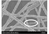
도 2에는 실시예 1에 따른 무전해 니켈/금 도금된 은 나노와이어가 기재에 매입된 폴리우레탄 기재의 SEM 사진이 나타내어진다. 도 2에 있어서, 은 나노와이어의 일부는 도금막이 형성되어 있지 않고, 외부 에너지(실시예 1에서는 열처리)에 의해 기재에 포함되어 있는 상태를 확인할 수 있다(흰선으로 둘러싼 부분). 또한, 표층에 노출되어 있는 은 나노와이어에만 도금막이 형성되어 있는 것도 동 도면으로부터 아울러 확인할 수 있다. FIG. 2 is a SEM photograph of a polyurethane base in which electroless nickel / gold plated silver nanowires according to Example 1 are embedded in a substrate. In Fig. 2, a part of the silver nanowire is not formed with a plated film, and the state of being contained in the substrate by external energy (heat treatment in the first embodiment) can be confirmed (a portion surrounded by a white line). It is also confirmed from the figure that a plated film is formed only on the silver nanowires exposed on the surface layer.
또한, 도 3에는 실시예 1에 따른 무전해 니켈/금 도금된 은 나노와이어의 단면 TEM 사진이 나타내어진다. 도 3에 있어서, 단면이 오각형인 은 나노와이어의 외층에 니켈이 약 10~30㎚의 두께로 도금되고, 또한 그 외측에 금 도금층이 형성되어 있는 것을 알 수 있다.(TEM상의 농담에 의해 각각의 층이 구별된다.) 3 is a cross-sectional TEM photograph of the electroless nickel / gold plated silver nanowire according to Example 1. In FIG. 3, it can be seen that nickel is plated to a thickness of about 10 to 30 nm on the outer layer of the silver nanowire having a five-sided cross section, and a gold plating layer is formed on the outer surface thereof. Layers are distinguished.)
실시예 2. Example 2.
혼합액의 유지 온도를 150℃로 변경한 것 이외에는 실시예 1과 마찬가지로 은 나노와이어를 제작하고, 기재를 PET 기재(루미러(등록상표) S, 폭 30㎜, 길이 50㎜, 두께 100㎛, 도레이사제)로 변경한 것 이외에는 마찬가지로 기판 전면에 은 나노와이어층을 형성하고, 그 후 레이저 에칭 가공에 의해 폭 10㎜, 길이 50㎜의 은 나노와이어의 패턴을 형성했다. Silver nanowires were prepared in the same manner as in Example 1 except that the holding temperature of the mixed solution was changed to 150 DEG C. The substrate was placed on a PET substrate (Lamier (registered trademark) S, 30 mm in width, 50 mm in length, A silver nanowire layer was formed on the entire surface of the substrate, and then a pattern of silver nanowires having a width of 10 mm and a length of 50 mm was formed by laser etching.
이 기재를 0.1 규정으로 조제한 희황산으로 10초간 처리, 소정량의 Pd 촉매액(JX 킨조쿠쇼지사제 KG-529)과 0.1 규정으로 조제한 희염산의 혼합액으로 1분간 처리, 그 후 100℃에서 5분간 열풍 순환식의 오븐에서 열처리, 무전해 Ni-P 도금액 (JX 킨조쿠쇼지사제 KG-531과 KG-531H)으로 80℃에서 10초간 처리, 소정량의 시안계 Au 도금액(JX 킨조쿠쇼지사제 KG-545Y)과 0.1~1g/L의 농도 범위에서 조제한 KAu(CN)2의 혼합액으로 80℃에서 1분간 처리를 행함으로써 무전해 도금하여 니켈층(15nm) 및 금층(15nm)을 형성했다.This substrate was treated with dilute sulfuric acid adjusted to 0.1 st for 10 seconds, treated with a predetermined amount of a Pd catalyst solution (KG-529, manufactured by JX Kinzoku Shoji Co., Ltd.) and a mixed solution of diluted hydrochloric acid prepared to 0.1 st for 1 minute, Heat treatment in a circulating oven, treatment at 80 캜 for 10 seconds with an electroless Ni-P plating solution (JX KINJOKUSHO Shoshi Co. KG-531 and KG-531H), and a predetermined amount of Au plating solution of cyan 545Y) and KAu (CN) 2 prepared in a concentration range of 0.1 to 1 g / L at 80 캜 for 1 minute to form a nickel layer (15 nm) and a gold layer (15 nm).
굽힘 시험으로서, 상기 샘플의 양단(폭측)을 탁상 인장 시험기(EZ-TEST, 시마즈세이사쿠쇼제, 척 사이 15㎜)의 상하 척부에 장착하고, 절곡부가 대략 반경 2.5㎜인 반원주 형상으로 될(은 나노와이어층이 절곡부의 외측으로 될) 때까지 상하동시키고, 이것을 사이클 시간 13.2초로 반복했다. 소정 횟수마다 양단에 장착된 단자를 통해서 저항값을 측정했다. As the bending test, both ends (widthwise sides) of the sample were mounted on upper and lower chuck portions of a tabletop tensile tester (EZ-TEST, Shimazu Seisakusho Co., Ltd., chuck 15 mm) The nanowire layer was moved up and down until it was outside the bent portion, and this was repeated with a cycle time of 13.2 seconds. Resistance values were measured through terminals mounted at both ends at predetermined times.
비교예 1. Comparative Example 1
도금 처리하지 않은 것 이외에는 실시예 2와 마찬가지의 처리에 의해 은 나노와이어를 도포한 PET 기재를 제작하고, 굽힘 시험 평가를 실시했다.A PET substrate coated with silver nanowires was produced in the same manner as in Example 2 except that the plating treatment was not performed, and the bending test evaluation was carried out.
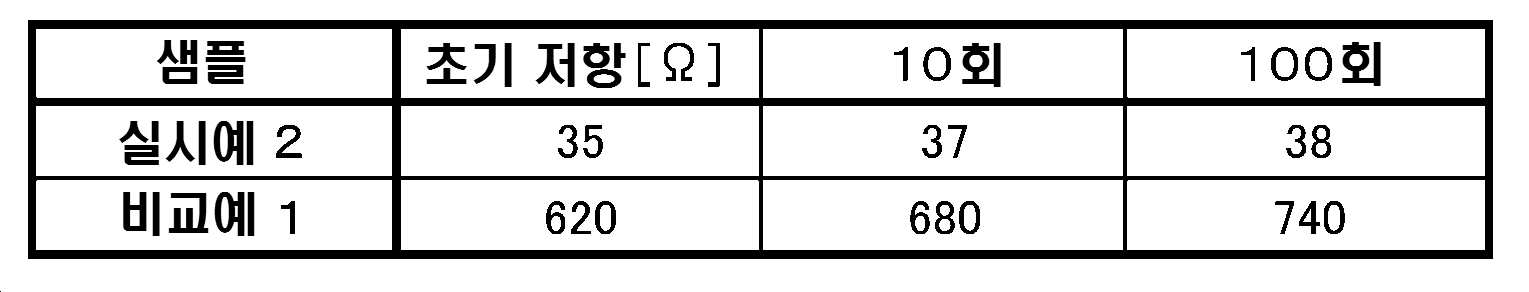
표 1에는 실시예 2 및 비교예 1에 따른 굽힘 시험 평가 결과를 나타낸다. 비교예 1에 있어서는 굴곡 횟수가 증가함에 따라 저항값이 상승해 가는 반면, 실시예 2에서는 굽힘 시험 중에서도 낮은 저항값을 유지하고 있으며, 기계적 강도가 향상되어 있는 것을 알 수 있다. Table 1 shows the results of the bending test evaluation according to Example 2 and Comparative Example 1. In Comparative Example 1, the resistance value rises as the number of bending times increases. On the other hand, in Example 2, a low resistance value is maintained in the bending test, and the mechanical strength is improved.
실시예 3. Example 3.
30㎜×30㎜×1㎜ 두께의 유리 기판에 dix(등록상표)-SR(KISCO사제)를 진공 하의 화학 증착에 의해 성막하고, 두께 3㎛의 파릴렌(등록상표)의 코팅막을 얻었다. 그 유리 기판 상에 형성된 파릴렌(등록상표)을 기재로서 사용하여 무전해 니켈 도금을 하지 않고 무전해 금 도금(약 5㎚)만 한 점 이외에는 실시예 1과 마찬가지로 처리하여 은 나노와이어의 일부가 파릴렌(등록상표)의 코팅막에 매입된 은 나노와이어층에 무전해 도금이 실시된 기재를 얻었다. Dix (registered trademark) -SR (manufactured by KISCO) was deposited on a glass substrate of 30 mm x 30 mm x 1 mm thickness by chemical vapor deposition under vacuum to obtain a coating film of Parylene (registered trademark) with a thickness of 3 m. Except that parylene (registered trademark) formed on the glass substrate was used as a substrate and electroless nickel plating was not performed but electroless gold plating (about 5 nm) was performed, so that a part of silver nanowires A substrate coated with electroless plating on a silver nanowire layer embedded in a coating film of Parylene (registered trademark) was obtained.
이어서, 이 기재 상에 무전해 도금이 실시된 나노와이어층을 레이저 에칭 가공함으로써 배선(폭 0.5㎜, 길이 4㎜)을 형성했다. 은의 마이그레이션을 가속시키기 위해 금 도금된 은 나노와이어 배선에 증류수를 배선 중앙부에 1방울 드롭하여 0.5㎜ 길이의 배선을 물방울로 덮은 후, 전류값 1mA에서 20분간 통전 후 10mA에서 20분간, 20mA에서 20분간, 30mA에서 20분간, 40mA에서 20분간으로 단계적으로 전류값을 증가시켜 통전하고, 도중의 배선 저항값 변화를 연속적으로 측정했다. 배선 저항 측정에 사용된 기기는 B2900A(Keysight사제)이며, 시험 전의 저항값 측정에는 미쓰비시애널리테크사제, LorestaGP T610을 사용했다. 배선의 초기 저항값은 150Ω였다. 내마이그레이션 시험 결과를 표 2에 나타낸다. Subsequently, a wire (0.5 mm in width, 4 mm in length) was formed by laser-etching the nanowire layer subjected to electroless plating on this substrate. In order to accelerate the migration of silver, 1 drop of distilled water was applied to the gold-plated silver nanowire wiring, and 0.5 mm-long wires were covered with water droplets. After the current was passed for 20 minutes at 1 mA, 20 mA at 20 mA, Minute, 30 mA for 20 minutes, and 40 mA for 20 minutes, and the change of the wiring resistance value in the middle was continuously measured. A device used for wiring resistance measurement was B2900A (manufactured by Keysight), and the resistance value before testing was LorestaGP T610 manufactured by Mitsubishi Electric Corporation. The initial resistance value of the wiring was 150 OMEGA. Table 2 shows the results of the migration test.
실시예 4.Example 4.
은 나노와이어의 도포량을 변경한 것 이외에는 실시예 3와 마찬가지로 처리한 유리 기판에 성막한 파릴렌(등록상표) 기재를 준비했다. 배선의 초기 저항값은 35Ω이었다. 내마이그레이션 시험 결과를 표 2에 나타낸다. 단면이 오각형인 은 나노와이어의 외측에 금이 5㎚ 이하의 두께로 도금되어 있다.(Registered trademark) substrate formed on a glass substrate treated in the same manner as in Example 3 except that the application amount of the nanowire was changed. The initial resistance value of the wiring was 35 OMEGA. Table 2 shows the results of the migration test. Gold is plated to a thickness of 5 nm or less on the outside of the silver nanowire whose cross section is a pentagon.
비교예 2. Comparative Example 2
무전해 금 도금을 하지 않는 것 이외에는 실시예 3과 마찬가지로 처리한 유리 기판에 성막한 파릴렌(등록상표) 기재를 준비하고, 내마이그레이션 시험을 실시했다. 배선의 초기 저항값은 140Ω였다. 내마이그레이션 시험 결과를 표 2에 나타낸다. A Parylene (registered trademark) substrate formed on a glass substrate treated in the same manner as in Example 3 was prepared except that electroless gold plating was not carried out, and a migration test was conducted. The initial resistance value of the wiring was 140 OMEGA. Table 2 shows the results of the migration test.
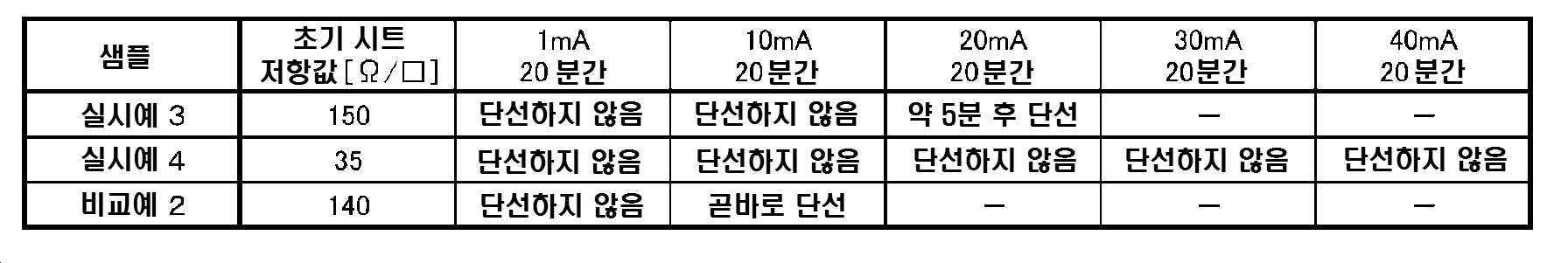
표 2에 나타내는 바와 같이, 비교예 2의 배선은 일정 전류(1mA)를 20분간 흘린 후, 10mA까지 전류값을 상승시키면 곧바로 배선은 단선했다. 한편, 실시예 3의 배선은 10mA의 일정 전류를 20분간 흘리고 있는 동안에는 단선하지 않고, 20mA로 전류값을 상승시킨 후에 단선했다. 마이그레이션이 진행되면, 배선의 일부가 용해되어 단자 사이의 단선이 생기는 현상을 평가하고 있다. 이것에 의해, 도금함으로써 은의 마이그레이션을 억제하는 효과가 있어 은 나노와이어의 내마이그레이션 특성이 향상되었다고 생각된다. 또한, 초기 저항값이 낮은, 실시예 4에서 준비한 배선은 40mA까지 전류값을 증가시켜도 단선이 확인되지 않고, 더욱 특성이 향상되어 있는 것을 알 수 있다. As shown in Table 2, in the wiring of Comparative Example 2, a constant current (1 mA) was passed for 20 minutes, and when the current value was increased to 10 mA, the wiring was disconnected immediately. On the other hand, the wiring of Example 3 was disconnected while a constant current of 10 mA was being applied for 20 minutes, and the current value was raised to 20 mA, followed by disconnection. As the migration progresses, a phenomenon occurs in which a part of the wiring is melted and a disconnection occurs between the terminals. Thus, migration of silver is inhibited by plating, and it is considered that the migration resistance of silver nanowires is improved. In addition, it can be seen that even when the current value is increased up to 40 mA in the wiring prepared in Example 4, in which the initial resistance value is low, disconnection is not confirmed and the characteristics are further improved.
실시예 5. Example 5.
도금 방법이 다른 것 이외, 실시예 1과 마찬가지 처리를 행하여 기재에 일부 은 나노와이어가 매입된 폴리우레탄 기재를 제작했다. The same treatment as in Example 1 was carried out except that the plating method was different, to fabricate a polyurethane base in which a part of the base material was embedded with nanowires.
은 나노와이어가 형성된 폴리우레탄 기재에 Ag 변색 제거제(닛폰일렉트로플레이팅·엔지니어스(EEJA)사제 EETOREX70)로 10초간 처리, 0.1 규정의 희황산으로 10초간 처리, 70℃의 Pt 도금액(EEJA사제 PRECIOUSFAB Pt3000)으로 처리를 실시하여 Pt 도금층을 형성했다. Pt 도금 중, 대극에 대하여 피도금물에는 약 1.0A/d㎡의 전류를 약 10초간 인가하고 있다. 이것에 의해, 은 나노와이어의 표면에 Pt층(약 1~100㎚)의 전해 도금층을 형성했다. Was treated with an Ag decolorizer (EETOREX 70, manufactured by EEJA) for 10 seconds, treated with 0.1 N dilute sulfuric acid for 10 seconds, and then immersed in a 70 캜 Pt plating solution (PRECIOUSFAB Pt3000 manufactured by EEJA) ) To form a plated Pt layer. During the Pt plating, about 1.0 A / dm < 2 > of current was applied to the object to be polished for about 10 seconds with respect to the counter electrode. Thus, an electroplating layer of a Pt layer (about 1 to 100 nm) was formed on the surface of the silver nanowire.
샘플의 관찰은 주사형 전자 현미경(FE-SEM SU8020, 히타치하이테크놀로지스사제) 및 원자 분해능 분석 전자 현미경(JEM-ARM200F, 닛폰덴시사제)을 이용하여 행했다. Samples were observed using a scanning electron microscope (FE-SEM SU8020, manufactured by Hitachi High-Technologies Corporation) and an atomic resolution analyzing electron microscope (JEM-ARM200F, manufactured by Nippon Denshi Co., Ltd.).
도 4에는 실시예 5에 따른 Pt 도금된 은 나노와이어가 기재에 매입된 폴리우레탄 기재의 SEM 사진이 나타내어진다. 도 4는 상기 주사형 전자 현미경(FE-SEM SU8020, 히타치하이테크놀로지스사제)을 사용하여 취득한 사진이다. 도 4에 있어서, 은 나노와이어의 일부는 도금막이 형성되어 있지 않고, 외부 에너지(실시예 1과 마찬가지의 열처리)에 의해 기재에 매입되어 있는 상태를 확인할 수 있다. 또한, 표층에 노출되어 있는 은 나노와이어에만 도금막이 형성되어 있는 것도 동 도면으로부터 아울러 확인할 수 있다. 4 shows a SEM photograph of a polyurethane base in which a Pt-plated silver nanowire according to Example 5 is embedded in a substrate. 4 is a photograph obtained using the scanning electron microscope (FE-SEM SU8020, manufactured by Hitachi High-Technologies Corporation). In FIG. 4, it can be seen that a part of the silver nanowire is not formed with a plated film and embedded in the substrate by external energy (the same heat treatment as in Embodiment 1). It is also confirmed from the figure that a plated film is formed only on the silver nanowires exposed on the surface layer.
또한, 도 5에는 실시예 5에 따른 Pt 도금된 은 나노와이어의 단면 TEM 사진이 나타내어진다. 도 5는 상기 원자 분해능 분석 전자 현미경(JEM-ARM200F, 닛폰덴시사제)을 사용하여 취득한 사진이다. 도 5에 있어서, 단면이 오각형인 은 나노와이어의 외층에 Pt가 평균 약 30㎚의 두께로 도금되어 있는 것을 알 수 있다(TEM상의 농담으로 각각의 층이 구별된다). 5 shows a cross-sectional TEM photograph of the Pt-plated silver nanowire according to Example 5. In FIG. 5 is a photograph obtained using the atomic resolution analyzing electron microscope (JEM-ARM200F, manufactured by Nippon Denshi Co., Ltd.). In FIG. 5, it can be seen that Pt is plated on the outer layer of the silver nanowire whose cross section is a pentagon, to an average thickness of about 30 nm (the layers are distinguished by the TEM image).
이어서, 실시예 3과 마찬가지로 레이저 에칭 가공으로 배선(폭 0.5㎜, 길이 4㎜)을 형성했다. 은의 마이그레이션을 가속화시키기 위해 백금 도금된 은 나노와이어 배선에 생리 식염수를 1방울 드롭하여 배선 0.5㎜ 길이를 물방울로 덮은 후 일정 전압 1V에서 20분간 전압을 인가하고, 도중의 배선 저항값 변화를 연속적으로 측정했다. 배선 저항 측정에 사용한 기기는 B2900A(Keysight사제)이며, 내마이그레이션 시험 결과를 표 3에 나타낸다. Then, wirings (width 0.5 mm, length 4 mm) were formed by laser etching as in the third embodiment. In order to accelerate the migration of silver, one drop of physiological saline was plated on the platinum-plated silver nanowire wiring, the wire 0.5 mm long was covered with water droplets, the voltage was applied at a constant voltage of 1 V for 20 minutes, Respectively. The equipment used for the wiring resistance measurement is B2900A (manufactured by Keysight), and the results of the migration test are shown in Table 3.
비교예 3. Comparative Example 3
전해 도금 처리하지 않은 은 나노와이어의 폴리우레탄 기재를 이용한 것 이외에는 실시예 5와 마찬가지의 평가를 행했다. 내마이그레이션 시험 결과를 표 3에 나타낸다. Evaluation was conducted in the same manner as in Example 5 except that silver nano wire of a polyurethane base not subjected to electrolytic plating was used. Table 3 shows the results of the migration test.
표 3에 나타내는 바와 같이, 비교예 3의 배선은 일정 전압(1V)을 5분간 인가하면 배선이 단선한 반면, 실시예 5의 배선은 1V의 일정 전압을 5분간 인가하고 있는 동안에는 단선하지 않고, 또한 동일 전압을 20분간 추가하여 인가해도 단선은 확인되지 않았다. 도금함으로써 은의 마이그레이션을 억제하는 효과가 있어 은 나노와이어의 내마이그레이션 특성이 향상되었다고 생각된다. As shown in Table 3, the wirings of Comparative Example 3 were disconnected when a constant voltage (1 V) was applied for 5 minutes while the wirings of Example 5 were not disconnected while a constant voltage of 1 V was applied for 5 minutes, Also, if the same voltage was further applied for 20 minutes, disconnection was not confirmed. It is believed that the plating has an effect of suppressing the migration of silver, and the migration characteristics of silver nanowires are improved.
실시예 6. Example 6.
실시예 1과 마찬가지로, 무전해 금 도금된 은 나노와이어/폴리우레탄 기재를 준비했다. 이 기재에, 펄스광 조사 장치 PulseForge3300(Novacentrix사제)를 이용하여 대기 실온 분위기 하 655V, 50msec의 조건에서 펄스광을 단발 조사했다.As in Example 1, an electroless gold-plated silver nanowire / polyurethane substrate was prepared. Pulsed light was irradiated onto this substrate by a pulse light irradiation apparatus PulseForge 3300 (manufactured by Novacentrix) at 655 V and 50 msec in an atmospheric room temperature atmosphere.
샘플(폭 15㎜, 길이 30㎜의 기판 상에 은 나노와이어층이 전면에 형성되어 있음)을 탁상 인장 시험기(EZ-test, 시마즈세이사쿠쇼사제, 시험 속도 : 15-60㎜/min, 척 간격 : 12㎜, 부하 : 0%-20% 변형)에 장착하여 반복하여 신축 시험을 행하고, 34410A multimeter and 11059A(Agilent Technologies사제)를 지그에 장착한 단자에서 샘플의 저항값을 측정했다. 신축 시험의 결과를 표 4에 나타낸다. A test sample (EZ-test, manufactured by Shimadzu Seisakusho Co., Ltd., test speed: 15-60 mm / min, chuck length: 30 mm) was placed on a sample 12 mm, load: 0% -20% strain), and the resistance of the sample was measured at a terminal fitted with a 34410A multimeter and 11059A (manufactured by Agilent Technologies) in a jig. Table 4 shows the results of the stretching test.
비교예 4. Comparative Example 4
무전해 도금 처리하지 않고, 또한 펄스광 조사(금속 나노와이어의 연결 처리)하지 않은 은 나노와이어의 폴리우레탄 기재를 이용한 것 이외에는 실시예 6과 마찬가지의 평가를 행했다. 신축 시험 결과를 표 4에 나타낸다.Evaluation was conducted in the same manner as in Example 6, except that silver nanowire polyurethane base without electroless plating treatment and without pulsed light irradiation (metal nanowire connection treatment) was used. Table 4 shows the results of the stretching test.

비교예 4에서는 20회의 신축 시험에서 단선이 발생되어 있는데 반해, 도금 및 펄스광 조사(금속 나노와이어의 연결 처리)한 실시예 6에서는 비교예 4에 비해 초기 저항값은 커지지만, 100회 후에도 저항값 측정이 가능하며, 내탄력성이 향상되어 있는 것을 알 수 있다. In Comparative Example 4, disconnection occurred in 20 elongation tests, whereas in Example 6 in which plating and pulsed light irradiation (metal nanowire connection treatment) were performed, the initial resistance value was larger than Comparative Example 4, Value can be measured, and the elasticity is improved.
실시예 7. Example 7.
은 나노와이어/에탄올 분산액의 도포량을 변경한 것 이외에는 실시예 1과 마찬가지로 은 나노와이어/폴리우레탄 기재를 준비하고, 실시예 2에 기재된 무전해 금 도금(무전해 Ni-P 도금 처리하지 않고 직접 시안계 Au 도금액(JX 킨조쿠쇼지사제 KG-545Y)과 KAu(CN)2의 혼합액으로 무전해 금 도금 처리)을 마찬가지로 실시했다. 도금 전후의 배선 저항은 B2900A(Keysight사제)를 이용하여 측정했다. 그 결과를 표 5에 나타낸다. Silver nanowire / polyurethane base material was prepared in the same manner as in Example 1, except that the application amount of the nanowire / ethanol dispersion was changed, and the electroless gold plating described in Example 2 (electroless Ni- Electroless gold plating treatment with a mixed solution of an Au plating solution (JX Kinzoku Shoji Co. KG-545Y) and KAu (CN) 2 ) was conducted in the same manner. The wiring resistance before and after plating was measured using B2900A (manufactured by Keysight). The results are shown in Table 5.
비교예 5. Comparative Example 5
기재 상에의 은 나노와이어/에탄올 분산액 도포 후의 열처리(100℃, 2분간) 및 Pd 촉매 처리 후의 오븐 열처리(100℃, 5분간) 모두 생략한 것 이외에는 실시예 7과 마찬가지로 은 나노와이어/폴리우레탄 기재를 준비하고, 무전해 금 도금을 실시하여 실시예 7과 마찬가지로 저항 평가했다. 그 결과를 표 5에 나타낸다.Similar to Example 7, except that both the heat treatment (100 占 폚 for 2 minutes) after application of the silver nanowire / ethanol dispersion and the oven heat treatment (100 占 폚, 5 minutes) after the Pd catalytic treatment were omitted on the substrate, silver nanowire / polyurethane A substrate was prepared and subjected to electroless gold plating, and the resistance was evaluated in the same manner as in Example 7. [ The results are shown in Table 5.

표 5로부터, 은 나노와이어/에탄올 분산액 도포 후의 열처리에 의해, 은 나노와이어가 기재 중에 매입되고, 그 후의 은 나노와이어에의 금 도금이 안정적으로 실시된 것을 알 수 있다. It can be seen from Table 5 that the silver nanowires were embedded in the substrate by the heat treatment after the application of the silver nanowire / ethanol dispersion, and the gold plating on the subsequent silver nanowires was stably carried out.
실시예 8. Example 8.
실시예 7과 마찬가지로 무전해 금 도금된 은 나노와이어/폴리우레탄 기재를 준비했다. 도금 전의 초기 저항값과 8,000시간 대기 중에 방치한 후의 저항값을 표 6에 나타낸다.Electroless gold-plated silver nanowire / polyurethane substrate was prepared as in Example 7. Table 6 shows the initial resistance value before plating and the resistance value after being left in the atmosphere for 8,000 hours.
비교예 6. Comparative Example 6
무전해 금 도금을 생략한 것 이외에는 실시예 7과 마찬가지로 무전해 금 도금을 하지 않는 은 나노와이어/폴리우레탄 기재를 준비했다. 초기 저항값과 8,000시간 대기 분위기 중에 방치한 후의 저항값을 표 6에 나타낸다. A silver nanowire / polyurethane base without electroless gold plating was prepared in the same manner as in Example 7 except that electroless gold plating was omitted. Table 6 shows the initial resistance value and the resistance value after being left in an atmospheric air for 8,000 hours.

표 6으로부터, 대기 하 보존에 있어서도 도금 후의 기재는 저항값에 변화가 없는 것으로부터도 대기 분위기 중 방치에 의한 산화, 황화의 영향을 받지 않는 내구성을 갖고 있는 것을 알 수 있다. It can be seen from Table 6 that even after the plating under atmosphere, the base material has durability not affected by oxidation and sulphation due to being left in an air atmosphere even though there is no change in the resistance value.
10 : 기재 12 : 금속 나노와이어층10: substrate 12: metal nanowire layer
Claims (9)
상기 금속 나노와이어의 적어도 일부가 연결되어 있는 금속 나노와이어층이 형성된 기재. The method according to claim 1,
And a metal nanowire layer having at least a part of the metal nanowires connected thereto.
상기 기재가 폴리우레탄, 실리콘 수지, 포화 폴리에스테르, 폴리카보네이트,폴리파라크실릴렌(파릴렌(등록상표)), 열가소성 폴리이미드, 폴리에테르술폰, 아크릴 수지, 폴리올레핀, 폴리염화비닐로 이루어지는 군 중 어느 하나인 금속 나노와이어층이 형성된 기재. 3. The method according to claim 1 or 2,
Wherein the substrate is selected from the group consisting of polyurethane, silicone resin, saturated polyester, polycarbonate, polyparaxylylene (parylene (registered trademark)), thermoplastic polyimide, polyether sulfone, acrylic resin, polyolefin, A substrate on which a metal nanowire layer is formed.
상기 금속 나노와이어를 구성하는 금속이 은 또는 구리인 금속 나노와이어층이 형성된 기재. 4. The method according to any one of claims 1 to 3,
And a metal nanowire layer in which the metal constituting the metal nanowire is silver or copper.
도금을 하는 공정의 전 또는 후에 상기 금속 나노와이어의 적어도 일부를 연결하는 공정을 더 포함하는 금속 나노와이어층이 형성된 기재의 제조 방법. 6. The method of claim 5,
And a step of connecting at least a part of the metal nanowires before or after the step of plating the metal nanowires.
상기 기재가 폴리우레탄, 실리콘 수지, 포화 폴리에스테르, 폴리카보네이트,폴리파라크실릴렌(파릴렌(등록상표)), 열가소성 폴리이미드, 폴리에테르술폰, 아크릴 수지, 폴리올레핀, 폴리염화비닐로 이루어지는 군 중 어느 하나인 금속 나노와이어층이 형성된 기재의 제조 방법. The method according to claim 5 or 6,
Wherein the substrate is selected from the group consisting of polyurethane, silicone resin, saturated polyester, polycarbonate, polyparaxylylene (parylene (registered trademark)), thermoplastic polyimide, polyether sulfone, acrylic resin, polyolefin, Wherein a metal nanowire layer is formed on the substrate.
상기 금속 나노와이어를 구성하는 금속이 은 또는 구리인 금속 나노와이어층이 형성된 기재의 제조 방법. 8. The method according to any one of claims 5 to 7,
Wherein a metal nanowire layer of which the metal constituting the metal nanowire is silver or copper is formed.
Applications Claiming Priority (3)
| Application Number | Priority Date | Filing Date | Title |
|---|---|---|---|
| JP2016055502 | 2016-03-18 | ||
| JPJP-P-2016-055502 | 2016-03-18 | ||
| PCT/JP2017/010264 WO2017159698A1 (en) | 2016-03-18 | 2017-03-14 | Substrate having metal nanowire layer formed thereon and method for manufacturing same |
Publications (1)
| Publication Number | Publication Date |
|---|---|
| KR20180098372A true KR20180098372A (en) | 2018-09-03 |
Family
ID=59850328
Family Applications (1)
| Application Number | Title | Priority Date | Filing Date |
|---|---|---|---|
| KR1020187021583A Ceased KR20180098372A (en) | 2016-03-18 | 2017-03-14 | Substrate having metal nanowire layer formed thereon and method for manufacturing the same |
Country Status (5)
| Country | Link |
|---|---|
| JP (1) | JP6956706B2 (en) |
| KR (1) | KR20180098372A (en) |
| CN (1) | CN108604482A (en) |
| TW (1) | TWI804462B (en) |
| WO (1) | WO2017159698A1 (en) |
Cited By (3)
| Publication number | Priority date | Publication date | Assignee | Title |
|---|---|---|---|---|
| KR20220026458A (en) * | 2020-08-25 | 2022-03-04 | 티피케이 어드밴스트 솔루션스 인코포레이티드 | Touch panel, manufacturing method of touch panel, and device thereof |
| KR20220026455A (en) * | 2020-08-25 | 2022-03-04 | 티피케이 어드밴스트 솔루션스 인코포레이티드 | Touch panel, manufacturing method of touch panel, and device thereof |
| US11347359B2 (en) | 2020-09-30 | 2022-05-31 | Tpk Advanced Solutions Inc. | Touch panel, manufacturing method of touch panel, and device thereof |
Families Citing this family (7)
| Publication number | Priority date | Publication date | Assignee | Title |
|---|---|---|---|---|
| JP7204195B2 (en) * | 2018-01-26 | 2023-01-16 | ユニチカ株式会社 | Plating primer and laminate using the same |
| CN108899279B (en) * | 2018-06-30 | 2021-03-02 | 广州国显科技有限公司 | Nano silver wire structure, preparation method thereof and display panel |
| CN110504068A (en) * | 2019-08-11 | 2019-11-26 | 东北师范大学 | A preparation method of transparent silver nanowire electrode with high conductivity and good stability |
| CN111333901B (en) * | 2020-03-04 | 2022-09-20 | 上海海事大学 | Flexible composite material and preparation method thereof and method for regulating and controlling negative dielectric property |
| CN113744931A (en) * | 2021-09-07 | 2021-12-03 | 浙江星隆新材料科技有限公司 | Preparation method of patterned conductive film |
| CN116313237A (en) * | 2023-03-24 | 2023-06-23 | 上海恩捷新材料科技有限公司 | Conductive thin film and preparation method thereof |
| CN117219796B (en) * | 2023-11-07 | 2024-02-13 | 武汉理工大学 | Pt-Pd dendrite hollow nanowire catalyst, and preparation method and application thereof |
Citations (3)
| Publication number | Priority date | Publication date | Assignee | Title |
|---|---|---|---|---|
| WO2009035059A1 (en) | 2007-09-12 | 2009-03-19 | Kuraray Co., Ltd. | Electroconductive film, electroconductive member, and process for producing electroconductive film |
| JP2013151752A (en) | 2013-03-01 | 2013-08-08 | Konica Minolta Inc | Method for manufacturing metal nano-wire |
| WO2014175163A1 (en) | 2013-04-26 | 2014-10-30 | 昭和電工株式会社 | Method for manufacturing electroconductive pattern and electroconductive pattern-formed substrate |
Family Cites Families (7)
| Publication number | Priority date | Publication date | Assignee | Title |
|---|---|---|---|---|
| JPH05151825A (en) * | 1991-11-27 | 1993-06-18 | Sekisui Chem Co Ltd | Conductive transparent body |
| TWI426531B (en) * | 2006-10-12 | 2014-02-11 | 坎畢歐科技公司 | Transparent conductor based on nanowire and its application |
| US20090321113A1 (en) * | 2007-04-20 | 2009-12-31 | Cambrios Technologies Corporation | High contrast transparent conductors and methods of forming the same |
| GB0908300D0 (en) * | 2009-05-14 | 2009-06-24 | Dupont Teijin Films Us Ltd | Polyester films |
| WO2011106438A1 (en) * | 2010-02-24 | 2011-09-01 | Cambrios Technologies Corporation | Nanowire-based transparent conductors and methods of patterning same |
| JP6700787B2 (en) * | 2012-12-07 | 2020-05-27 | スリーエム イノベイティブ プロパティズ カンパニー | Method for producing transparent conductor on substrate |
| JP6022424B2 (en) * | 2013-08-01 | 2016-11-09 | 日本写真印刷株式会社 | Transparent conductive sheet and touch panel using transparent conductive sheet |
-
2017
- 2017-03-14 JP JP2018505962A patent/JP6956706B2/en active Active
- 2017-03-14 CN CN201780009177.XA patent/CN108604482A/en active Pending
- 2017-03-14 KR KR1020187021583A patent/KR20180098372A/en not_active Ceased
- 2017-03-14 WO PCT/JP2017/010264 patent/WO2017159698A1/en not_active Ceased
- 2017-03-16 TW TW106108759A patent/TWI804462B/en active
Patent Citations (3)
| Publication number | Priority date | Publication date | Assignee | Title |
|---|---|---|---|---|
| WO2009035059A1 (en) | 2007-09-12 | 2009-03-19 | Kuraray Co., Ltd. | Electroconductive film, electroconductive member, and process for producing electroconductive film |
| JP2013151752A (en) | 2013-03-01 | 2013-08-08 | Konica Minolta Inc | Method for manufacturing metal nano-wire |
| WO2014175163A1 (en) | 2013-04-26 | 2014-10-30 | 昭和電工株式会社 | Method for manufacturing electroconductive pattern and electroconductive pattern-formed substrate |
Cited By (3)
| Publication number | Priority date | Publication date | Assignee | Title |
|---|---|---|---|---|
| KR20220026458A (en) * | 2020-08-25 | 2022-03-04 | 티피케이 어드밴스트 솔루션스 인코포레이티드 | Touch panel, manufacturing method of touch panel, and device thereof |
| KR20220026455A (en) * | 2020-08-25 | 2022-03-04 | 티피케이 어드밴스트 솔루션스 인코포레이티드 | Touch panel, manufacturing method of touch panel, and device thereof |
| US11347359B2 (en) | 2020-09-30 | 2022-05-31 | Tpk Advanced Solutions Inc. | Touch panel, manufacturing method of touch panel, and device thereof |
Also Published As
| Publication number | Publication date |
|---|---|
| JPWO2017159698A1 (en) | 2019-01-24 |
| CN108604482A (en) | 2018-09-28 |
| WO2017159698A1 (en) | 2017-09-21 |
| TWI804462B (en) | 2023-06-11 |
| JP6956706B2 (en) | 2021-11-02 |
| TW201801901A (en) | 2018-01-16 |
Similar Documents
| Publication | Publication Date | Title |
|---|---|---|
| KR20180098372A (en) | Substrate having metal nanowire layer formed thereon and method for manufacturing the same | |
| US12336115B2 (en) | Liquid metal fusion with conductive inks and pastes | |
| An et al. | Self-Junctioned Copper Nanofiber Transparent Flexible Conducting Film via Electrospinning and Electroplating. | |
| Zhang et al. | Conformal manufacturing of soft deformable sensors on the curved surface | |
| KR20160014703A (en) | Transparent electrode and method for producing same | |
| CN108701505A (en) | The forming method for the wiring that retractility conductor piece, the retractility conductor piece with cementability, the retractility conductor on cloth and silk are constituted | |
| JP7028564B2 (en) | Flexible wiring board or flexible conductor structure, its manufacturing method, and electronic devices including it. | |
| CN113630915A (en) | Composite processing method for flexibly customizing high-adjustable flexible micro-heater and micro-heater | |
| Zhang et al. | Hierarchically Oriented Jellyfish‐Like Gold Nanowires Film for Elastronics | |
| KR20200041799A (en) | Conductive Fiber and the Fabrication Method Thereof | |
| Abdulrhman et al. | Routes towards manufacturing biodegradable electronics with polycaprolactone (PCL) via direct light writing and electroless plating | |
| CN107610815A (en) | A kind of nano silver wire clear composite coating and preparation method thereof | |
| JP7837987B2 (en) | Additive manufacturing system, method for forming an additive manufacturing system, and method for forming a composite structure | |
| JP5967778B2 (en) | Method for depositing conductive polymer-metal composite, conductive polymer-metal composite, method for forming conductive wiring pattern on flexible substrate, and flexible substrate | |
| Xie et al. | A facile and universally applicable additive strategy for fabrication of high-quality copper patterns based on a homogeneous Ag catalyst ink | |
| KR20090126825A (en) | Core Shell Nanowires and Manufacturing Method Thereof | |
| TWI552171B (en) | Conductive film and manufacturing method for preparing the same | |
| KR101221980B1 (en) | Soldable and flexible electrode and method for preparing the same | |
| JP6542572B2 (en) | Stretchable conductive film and method of producing stretchable conductive film | |
| Zhou et al. | Chemically activated Ag-embedded bridged-layer for copper pattern addition on PET film | |
| KR102439113B1 (en) | Manufacturing method of composite material plated with network-type nano-metal layer through silica crack and wearable electronics carbon fiber manufactured therefrom | |
| JP2008027636A (en) | Method for producing transparent conductive film | |
| CN116655977B (en) | Fabrication method and device of flexible multifunctional thin film based on reliable interface bonding | |
| RU2770237C1 (en) | Transceiver device and method for its manufacture | |
| TWI620834B (en) | Flexible light-emitting apparatus and method of fabricating the same |
Legal Events
| Date | Code | Title | Description |
|---|---|---|---|
| A201 | Request for examination | ||
| AMND | Amendment | ||
| PA0105 | International application |
Patent event date: 20180726 Patent event code: PA01051R01D Comment text: International Patent Application |
|
| PA0201 | Request for examination | ||
| PG1501 | Laying open of application | ||
| E902 | Notification of reason for refusal | ||
| PE0902 | Notice of grounds for rejection |
Comment text: Notification of reason for refusal Patent event date: 20191121 Patent event code: PE09021S01D |
|
| AMND | Amendment | ||
| E601 | Decision to refuse application | ||
| PE0601 | Decision on rejection of patent |
Patent event date: 20200526 Comment text: Decision to Refuse Application Patent event code: PE06012S01D Patent event date: 20191121 Comment text: Notification of reason for refusal Patent event code: PE06011S01I |
|
| X091 | Application refused [patent] | ||
| AMND | Amendment | ||
| PX0901 | Re-examination |
Patent event code: PX09011S01I Patent event date: 20200526 Comment text: Decision to Refuse Application Patent event code: PX09012R01I Patent event date: 20200121 Comment text: Amendment to Specification, etc. Patent event code: PX09012R01I Patent event date: 20180726 Comment text: Amendment to Specification, etc. |
|
| PX0601 | Decision of rejection after re-examination |
Comment text: Decision to Refuse Application Patent event code: PX06014S01D Patent event date: 20200721 Comment text: Amendment to Specification, etc. Patent event code: PX06012R01I Patent event date: 20200625 Comment text: Decision to Refuse Application Patent event code: PX06011S01I Patent event date: 20200526 Comment text: Amendment to Specification, etc. Patent event code: PX06012R01I Patent event date: 20200121 Comment text: Notification of reason for refusal Patent event code: PX06013S01I Patent event date: 20191121 Comment text: Amendment to Specification, etc. Patent event code: PX06012R01I Patent event date: 20180726 |
|
| X601 | Decision of rejection after re-examination |