KR20180098132A - 기판 처리 방법 및 기판 처리 장치 - Google Patents
기판 처리 방법 및 기판 처리 장치 Download PDFInfo
- Publication number
- KR20180098132A KR20180098132A KR1020180011366A KR20180011366A KR20180098132A KR 20180098132 A KR20180098132 A KR 20180098132A KR 1020180011366 A KR1020180011366 A KR 1020180011366A KR 20180011366 A KR20180011366 A KR 20180011366A KR 20180098132 A KR20180098132 A KR 20180098132A
- Authority
- KR
- South Korea
- Prior art keywords
- substrate
- liquid
- liquid film
- periphery
- surface tension
- Prior art date
- Legal status (The legal status is an assumption and is not a legal conclusion. Google has not performed a legal analysis and makes no representation as to the accuracy of the status listed.)
- Granted
Links
Images


Classifications
-
- H—ELECTRICITY
- H10—SEMICONDUCTOR DEVICES; ELECTRIC SOLID-STATE DEVICES NOT OTHERWISE PROVIDED FOR
- H10P—GENERIC PROCESSES OR APPARATUS FOR THE MANUFACTURE OR TREATMENT OF DEVICES COVERED BY CLASS H10
- H10P72/00—Handling or holding of wafers, substrates or devices during manufacture or treatment thereof
- H10P72/04—Apparatus for manufacture or treatment
- H10P72/0402—Apparatus for fluid treatment
- H10P72/0406—Apparatus for fluid treatment for cleaning followed by drying, rinsing, stripping, blasting or the like
- H10P72/0408—Apparatus for fluid treatment for cleaning followed by drying, rinsing, stripping, blasting or the like for drying
-
- H01L21/02052—
-
- H—ELECTRICITY
- H10—SEMICONDUCTOR DEVICES; ELECTRIC SOLID-STATE DEVICES NOT OTHERWISE PROVIDED FOR
- H10P—GENERIC PROCESSES OR APPARATUS FOR THE MANUFACTURE OR TREATMENT OF DEVICES COVERED BY CLASS H10
- H10P70/00—Cleaning of wafers, substrates or parts of devices
- H10P70/10—Cleaning before device manufacture, i.e. Begin-Of-Line process
- H10P70/15—Cleaning before device manufacture, i.e. Begin-Of-Line process by wet cleaning only
-
- H—ELECTRICITY
- H10—SEMICONDUCTOR DEVICES; ELECTRIC SOLID-STATE DEVICES NOT OTHERWISE PROVIDED FOR
- H10P—GENERIC PROCESSES OR APPARATUS FOR THE MANUFACTURE OR TREATMENT OF DEVICES COVERED BY CLASS H10
- H10P70/00—Cleaning of wafers, substrates or parts of devices
- H10P70/20—Cleaning during device manufacture
-
- H01L21/02307—
-
- H01L21/6704—
-
- H01L21/6715—
-
- H01L21/67242—
-
- H—ELECTRICITY
- H10—SEMICONDUCTOR DEVICES; ELECTRIC SOLID-STATE DEVICES NOT OTHERWISE PROVIDED FOR
- H10P—GENERIC PROCESSES OR APPARATUS FOR THE MANUFACTURE OR TREATMENT OF DEVICES COVERED BY CLASS H10
- H10P14/00—Formation of materials, e.g. in the shape of layers or pillars
- H10P14/60—Formation of materials, e.g. in the shape of layers or pillars of insulating materials
- H10P14/65—Formation of materials, e.g. in the shape of layers or pillars of insulating materials characterised by treatments performed before or after the formation of the materials
- H10P14/6502—Formation of materials, e.g. in the shape of layers or pillars of insulating materials characterised by treatments performed before or after the formation of the materials of treatments performed before formation of the materials
- H10P14/6508—Formation of materials, e.g. in the shape of layers or pillars of insulating materials characterised by treatments performed before or after the formation of the materials of treatments performed before formation of the materials by exposure to a liquid
-
- H—ELECTRICITY
- H10—SEMICONDUCTOR DEVICES; ELECTRIC SOLID-STATE DEVICES NOT OTHERWISE PROVIDED FOR
- H10P—GENERIC PROCESSES OR APPARATUS FOR THE MANUFACTURE OR TREATMENT OF DEVICES COVERED BY CLASS H10
- H10P70/00—Cleaning of wafers, substrates or parts of devices
- H10P70/20—Cleaning during device manufacture
- H10P70/23—Cleaning during device manufacture during, before or after processing of insulating materials
- H10P70/234—Cleaning during device manufacture during, before or after processing of insulating materials the processing being the formation of vias or contact holes
-
- H—ELECTRICITY
- H10—SEMICONDUCTOR DEVICES; ELECTRIC SOLID-STATE DEVICES NOT OTHERWISE PROVIDED FOR
- H10P—GENERIC PROCESSES OR APPARATUS FOR THE MANUFACTURE OR TREATMENT OF DEVICES COVERED BY CLASS H10
- H10P70/00—Cleaning of wafers, substrates or parts of devices
- H10P70/50—Cleaning of wafers, substrates or parts of devices characterised by the part to be cleaned
-
- H—ELECTRICITY
- H10—SEMICONDUCTOR DEVICES; ELECTRIC SOLID-STATE DEVICES NOT OTHERWISE PROVIDED FOR
- H10P—GENERIC PROCESSES OR APPARATUS FOR THE MANUFACTURE OR TREATMENT OF DEVICES COVERED BY CLASS H10
- H10P72/00—Handling or holding of wafers, substrates or devices during manufacture or treatment thereof
- H10P72/04—Apparatus for manufacture or treatment
- H10P72/0402—Apparatus for fluid treatment
- H10P72/0406—Apparatus for fluid treatment for cleaning followed by drying, rinsing, stripping, blasting or the like
- H10P72/0411—Apparatus for fluid treatment for cleaning followed by drying, rinsing, stripping, blasting or the like for wet cleaning or washing
- H10P72/0414—Apparatus for fluid treatment for cleaning followed by drying, rinsing, stripping, blasting or the like for wet cleaning or washing using mainly spraying means, e.g. nozzles
-
- H—ELECTRICITY
- H10—SEMICONDUCTOR DEVICES; ELECTRIC SOLID-STATE DEVICES NOT OTHERWISE PROVIDED FOR
- H10P—GENERIC PROCESSES OR APPARATUS FOR THE MANUFACTURE OR TREATMENT OF DEVICES COVERED BY CLASS H10
- H10P72/00—Handling or holding of wafers, substrates or devices during manufacture or treatment thereof
- H10P72/04—Apparatus for manufacture or treatment
- H10P72/0448—Apparatus for applying a liquid, a resin, an ink or the like
-
- H—ELECTRICITY
- H10—SEMICONDUCTOR DEVICES; ELECTRIC SOLID-STATE DEVICES NOT OTHERWISE PROVIDED FOR
- H10P—GENERIC PROCESSES OR APPARATUS FOR THE MANUFACTURE OR TREATMENT OF DEVICES COVERED BY CLASS H10
- H10P72/00—Handling or holding of wafers, substrates or devices during manufacture or treatment thereof
- H10P72/06—Apparatus for monitoring, sorting, marking, testing or measuring
-
- H—ELECTRICITY
- H10—SEMICONDUCTOR DEVICES; ELECTRIC SOLID-STATE DEVICES NOT OTHERWISE PROVIDED FOR
- H10P—GENERIC PROCESSES OR APPARATUS FOR THE MANUFACTURE OR TREATMENT OF DEVICES COVERED BY CLASS H10
- H10P72/00—Handling or holding of wafers, substrates or devices during manufacture or treatment thereof
- H10P72/70—Handling or holding of wafers, substrates or devices during manufacture or treatment thereof for supporting or gripping
- H10P72/76—Handling or holding of wafers, substrates or devices during manufacture or treatment thereof for supporting or gripping using mechanical means, e.g. clamps or pinches
- H10P72/7604—Handling or holding of wafers, substrates or devices during manufacture or treatment thereof for supporting or gripping using mechanical means, e.g. clamps or pinches the wafers being placed on a susceptor, stage or support
- H10P72/7608—Handling or holding of wafers, substrates or devices during manufacture or treatment thereof for supporting or gripping using mechanical means, e.g. clamps or pinches the wafers being placed on a susceptor, stage or support characterised by a plurality of separate clamping members, e.g. clamping fingers
Landscapes
- Cleaning Or Drying Semiconductors (AREA)
- Exposure Of Semiconductors, Excluding Electron Or Ion Beam Exposure (AREA)
Abstract
Description
도 2는, 상기 기판 처리 장치에 구비된 처리 유닛의 구성예를 설명하기 위한 모식도이다.
도 3은, 도 2의 III-III선에 따른 단면의 모식도이다.
도 4는, 차단 부재에 설치된 근접 부재의 주변의 모식도이며, 차단 부재가 하부 위치에 있는 상태를 나타내고 있다.
도 5는, 상기 기판 처리 장치의 주요부의 전기적 구성을 설명하기 위한 블럭도이다.
도 6은, 상기 기판 처리 장치에 의한 기판 처리의 일례를 설명하기 위한 흐름도이다.
도 7은, 상기 기판 처리의 유기용제 처리의 일례를 설명하기 위한 흐름도이다.
도 8a~도 8e는, 유기용제 처리(도 6의 S4)의 모습을 설명하기 위한 모식적인 단면도이다.
도 9a는, 확대 배제 공정에 있어서의 개구의 주연 부근을 모식적으로 나타낸 도면이다.
도 9b는, 회전하고 있지 않은 상태의 기판 상에 적하된 유기용제의 액적 부근을 모식적으로 나타낸 도면이다.
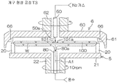
도 10a는, 유기용제 처리(도 6의 S4)의 액막 접촉 공정에 있어서의 근접 부재의 주변의 종단면의 모식도이다.
도 10b는, 유기용제 처리(도 6의 S4)의 액막 접촉 공정에 있어서의 근접 부재의 주변의 횡단면의 모식도이다.
도 11은, 이 발명의 제2 실시 형태에 따른 기판 처리 장치의 베이스의 주변을 평면에서 보았을 때의 모식도이다.
도 12는, 제2 실시 형태에 따른 기판 처리 장치에 구비된 처리 유닛의 구성예를 나타내는 모식도이며, 도 11의 XII-XII선에 따른 단면을 나타내고 있다.
도 13a~도 13b는, 제2 실시 형태에 따른 기판 처리 장치에 의한 기판 처리에 있어서의 유기용제 처리(도 6의 S4)의 모습을 설명하기 위한 모식적인 단면도이다.
도 14는, 표면장력에 의한 패턴 도괴의 원리를 설명하기 위한 도해적인 단면도이다.
Claims (18)
- 기판을 수평하게 유지하는 기판 유지 공정과,
상기 기판의 상면에 물을 함유하는 처리액을 공급하는 처리액 공급 공정과,
물보다 낮은 표면장력을 갖는 저표면장력 액체를 상기 기판의 상면에 공급함으로써, 상기 저표면장력 액체로 상기 처리액을 치환하는 치환 공정과,
상기 치환 공정 후에, 상기 기판의 상면에 대한 상기 저표면장력 액체의 공급을 계속함으로써, 상기 기판의 상면에 상기 저표면장력 액체의 액막을 형성하는 액막 형성 공정과,
상기 액막의 중앙 영역에 개구를 형성하는 개구 형성 공정과,
상기 개구를 상기 기판의 주연을 향해 넓힘으로써 상기 액막을 상기 기판의 상면으로부터 배제하는 확대 배제 공정과,
상기 개구 형성 공정의 개시 후에, 근접 부재를 상기 기판의 주연에 근접시킴으로써, 상기 근접 부재를 상기 액막에 접촉시키는 액막 접촉 공정을 포함하는, 기판 처리 방법. - 청구항 1에 있어서,
상기 액막 접촉 공정이, 상기 확대 배제 공정과 병행하여 실행되는, 기판 처리 방법. - 청구항 1 또는 청구항 2에 있어서,
상기 액막 접촉 공정에 있어서, 상기 근접 부재와 상기 기판의 주연 사이에 간극이 형성되도록, 상기 근접 부재를 상기 기판의 주연에 근접시키는, 기판 처리 방법. - 청구항 1 또는 청구항 2에 있어서,
상기 기판 유지 공정이, 베이스의 상면에 설치되고 상기 기판의 주연을 유지하는 기판 유지구에 상기 기판의 주연을 유지시키는 공정을 포함하고,
상기 액막 접촉 공정에 있어서, 상기 기판의 주연에 있어서 상기 기판 유지구에 의해 유지된 부분과는 다른 부분에, 상기 근접 부재를 근접시키는, 기판 처리 방법. - 청구항 4에 있어서,
상기 근접 부재가, 상기 베이스의 상면에 설치된 근접 핀이며,
상기 액막 접촉 공정에 있어서, 상기 기판의 바깥쪽으로부터 상기 근접 핀을 상기 기판의 주연에 접근시키는, 기판 처리 방법. - 청구항 1 또는 청구항 2에 있어서,
상기 근접 부재가, 상기 기판의 상면에 대향하며 상기 기판과의 사이의 분위기를 주위의 분위기로부터 차단하는 차단 부재에 설치되고,
상기 액막 접촉 공정에 있어서, 상기 기판의 주연에 상기 차단 부재를 상방으로부터 접근시키는, 기판 처리 방법. - 청구항 1 또는 청구항 2에 있어서,
상기 액막 형성 공정이, 상기 기판 상의 상기 저표면장력 액체의 온도를 상기 저표면장력 액체의 비점 이하로 유지한 상태로, 상기 기판의 상면에 상기 액막을 형성하는 공정을 포함하는, 기판 처리 방법. - 청구항 7에 있어서,
상기 개구 형성 공정이, 상기 액막의 중앙 영역의 온도를, 상기 액막 형성 공정에 있어서의 상기 액막의 온도보다 높게 함으로써, 상기 액막에 상기 개구를 형성하는 공정을 포함하는, 기판 처리 방법. - 청구항 7에 있어서,
상기 확대 배제 공정이, 상기 개구의 주연에 위치하는 상기 액막의 기액 계면에 있어서, 상기 기판으로부터 멀어지는 방향의 대류가 발생하도록 상기 기판을 가열하고, 그로 인해, 상기 개구를 상기 기판의 주연을 향해 넓히는 공정을 포함하는, 기판 처리 방법. - 기판을 수평하게 유지하는 기판 유지 유닛과,
상기 기판에 물을 함유하는 처리액을 공급하는 처리액 공급 유닛과,
물보다 낮은 표면장력을 갖는 저표면장력 액체를 상기 기판에 공급하는 저표면장력 액체 공급 유닛과,
상기 기판의 주연에 근접하는 근접 부재와,
상기 근접 부재와 상기 기판의 상대 위치를 변경하는 상대 위치 변경 유닛과,
상기 기판 유지 유닛, 상기 처리액 공급 유닛, 상기 저표면장력 액체 공급 유닛 및 상기 상대 위치 변경 유닛을 제어하는 컨트롤러를 포함하고,
상기 컨트롤러가, 상기 기판 유지 유닛에 의해 기판을 수평하게 유지하는 기판 유지 공정과, 상기 기판의 상면을 향해 상기 처리액 공급 유닛으로부터 상기 처리액을 공급하는 처리액 공급 공정과, 상기 기판의 상면을 향해 상기 저표면장력 액체 공급 유닛으로부터 상기 저표면장력 액체를 공급함으로써, 상기 저표면장력 액체로 상기 처리액을 치환하는 치환 공정과, 상기 치환 공정 후에, 상기 저표면장력 액체 공급 유닛으로부터 상기 기판의 상면에 대한 상기 저표면장력 액체의 공급을 계속함으로써, 상기 기판의 상면에 상기 저표면장력 액체의 액막을 형성하는 액막 형성 공정과, 상기 액막의 중앙 영역에 개구를 형성하는 개구 형성 공정과, 상기 개구를 상기 기판의 주연을 향해 넓히는 확대 배제 공정과, 상기 개구 형성 공정의 개시 후에, 상기 상대 위치 변경 유닛에 의해 상기 근접 부재와 상기 기판의 상대 위치를 변경함으로써, 상기 근접 부재를 상기 액막에 접촉시키는 액막 접촉 공정을 실행하도록 프로그램되어 있는, 기판 처리 장치. - 청구항 10에 있어서,
상기 컨트롤러가, 상기 확대 배제 공정과 병행하여 상기 액막 접촉 공정을 실행하도록 프로그램되어 있는, 기판 처리 장치. - 청구항 10 또는 청구항 11에 있어서,
상기 컨트롤러가, 상기 액막 접촉 공정에 있어서, 상기 상대 위치 변경 유닛을 제어하여, 상기 근접 부재와 상기 기판의 주연 사이에 간극이 형성되도록, 상기 근접 부재를 상기 기판의 주연에 접근시키도록 프로그램되어 있는, 기판 처리 장치. - 청구항 10 또는 청구항 11에 있어서,
상기 기판 유지 유닛이, 베이스의 상면에 설치되고 상기 기판의 주연을 유지하는 기판 유지구를 포함하고,
상기 컨트롤러가, 상기 액막 접촉 공정에 있어서, 상기 상대 위치 변경 유닛을 제어하여, 상기 기판의 주연에 있어서 상기 기판 유지구에 의해 유지된 부분과는 다른 부분에, 상기 근접 부재를 근접시키도록 프로그램되어 있는, 기판 처리 장치. - 청구항 13에 있어서,
상기 근접 부재가, 상기 베이스의 상면에 설치된 근접 핀이며,
상기 컨트롤러가, 상기 액막 접촉 공정에 있어서, 상기 상대 위치 변경 유닛을 제어하여, 상기 기판의 바깥쪽으로부터 상기 근접 부재를 상기 기판의 주연에 근접시키도록 프로그램되어 있는, 기판 처리 장치. - 청구항 10 또는 청구항 11에 있어서,
상기 근접 부재가, 상기 기판의 상면에 대향하며 상기 기판과의 사이의 분위기를 주위의 분위기로부터 차단하는 차단 부재에 설치되고,
상기 컨트롤러가, 상기 액막 접촉 공정에 있어서, 상기 기판의 주연에 상기 근접 부재를 상방으로부터 접근시키도록 프로그램되어 있는, 기판 처리 장치. - 청구항 10 또는 청구항 11에 있어서,
상기 기판을 가열하는 기판 가열 유닛을 더 포함하고,
상기 컨트롤러가, 상기 액막 형성 공정에 있어서, 상기 기판 가열 유닛을 제어하여, 상기 기판 상의 상기 저표면장력 액체의 온도를 상기 저표면장력 액체의 비점 이하로 유지하도록 프로그램되어 있는, 기판 처리 장치. - 청구항 16에 있어서,
상기 컨트롤러가, 상기 개구 형성 공정에 있어서, 상기 기판 가열 유닛을 제어하여, 상기 액막의 중앙 영역의 온도를, 상기 액막 형성 공정에 있어서의 상기 액막의 온도보다 높게 함으로써, 상기 액막에 상기 개구를 형성하도록 프로그램되어 있는, 기판 처리 장치. - 청구항 16에 있어서,
상기 컨트롤러가, 상기 확대 배제 공정에 있어서, 상기 기판 가열 유닛을 제어하여, 상기 개구의 주연에 위치하는 상기 액막의 기액 계면에 있어서, 상기 기판으로부터 멀어지는 방향의 대류가 발생하도록 상기 기판을 가열하고, 그로 인해, 상기 개구를 상기 기판의 주연을 향해 넓히도록 프로그램되어 있는, 기판 처리 장치.
Applications Claiming Priority (2)
| Application Number | Priority Date | Filing Date | Title |
|---|---|---|---|
| JP2017033609A JP6916003B2 (ja) | 2017-02-24 | 2017-02-24 | 基板処理方法および基板処理装置 |
| JPJP-P-2017-033609 | 2017-02-24 |
Publications (2)
| Publication Number | Publication Date |
|---|---|
| KR20180098132A true KR20180098132A (ko) | 2018-09-03 |
| KR102062444B1 KR102062444B1 (ko) | 2020-01-03 |
Family
ID=63246892
Family Applications (1)
| Application Number | Title | Priority Date | Filing Date |
|---|---|---|---|
| KR1020180011366A Active KR102062444B1 (ko) | 2017-02-24 | 2018-01-30 | 기판 처리 방법 및 기판 처리 장치 |
Country Status (5)
| Country | Link |
|---|---|
| US (1) | US10790166B2 (ko) |
| JP (1) | JP6916003B2 (ko) |
| KR (1) | KR102062444B1 (ko) |
| CN (1) | CN108511319B (ko) |
| TW (1) | TWI667076B (ko) |
Families Citing this family (5)
| Publication number | Priority date | Publication date | Assignee | Title |
|---|---|---|---|---|
| JP7201494B2 (ja) * | 2019-03-20 | 2023-01-10 | 株式会社Screenホールディングス | 基板処理方法および基板処理装置 |
| JP7241589B2 (ja) * | 2019-04-04 | 2023-03-17 | 東京エレクトロン株式会社 | 基板処理方法および基板処理装置 |
| CN113053728B (zh) * | 2019-12-27 | 2024-08-27 | 株式会社斯库林集团 | 基板处理方法以及基板处理装置 |
| JP7745359B2 (ja) * | 2021-04-16 | 2025-09-29 | 株式会社Screenホールディングス | 基板処理方法、基板処理装置および乾燥処理液 |
| JP2024171015A (ja) * | 2023-05-29 | 2024-12-11 | 株式会社Screenホールディングス | 基板処理装置 |
Citations (2)
| Publication number | Priority date | Publication date | Assignee | Title |
|---|---|---|---|---|
| JP2010050143A (ja) * | 2008-08-19 | 2010-03-04 | Dainippon Screen Mfg Co Ltd | 基板処理方法および基板処理装置 |
| KR20150101951A (ko) * | 2014-02-27 | 2015-09-04 | 가부시키가이샤 스크린 홀딩스 | 기판 처리 장치 및 기판 처리 방법 |
Family Cites Families (28)
| Publication number | Priority date | Publication date | Assignee | Title |
|---|---|---|---|---|
| US7000622B2 (en) * | 2002-09-30 | 2006-02-21 | Lam Research Corporation | Methods and systems for processing a bevel edge of a substrate using a dynamic liquid meniscus |
| US6770151B1 (en) * | 2001-07-13 | 2004-08-03 | Lam Research Corporation | Drying a substrate using a combination of substrate processing technologies |
| US7156111B2 (en) * | 2001-07-16 | 2007-01-02 | Akrion Technologies, Inc | Megasonic cleaning using supersaturated cleaning solution |
| US20030192577A1 (en) * | 2002-04-11 | 2003-10-16 | Applied Materials, Inc. | Method and apparatus for wafer cleaning |
| US20030192570A1 (en) * | 2002-04-11 | 2003-10-16 | Applied Materials, Inc. | Method and apparatus for wafer cleaning |
| US20040084144A1 (en) * | 2002-08-21 | 2004-05-06 | Dainippon Screen Mfg. Co., Ltd. | Substrate processing apparatus and substrate processing method |
| US7520285B2 (en) * | 2002-09-30 | 2009-04-21 | Lam Research Corporation | Apparatus and method for processing a substrate |
| US7198055B2 (en) * | 2002-09-30 | 2007-04-03 | Lam Research Corporation | Meniscus, vacuum, IPA vapor, drying manifold |
| US7614411B2 (en) * | 2002-09-30 | 2009-11-10 | Lam Research Corporation | Controls of ambient environment during wafer drying using proximity head |
| JP4889331B2 (ja) * | 2006-03-22 | 2012-03-07 | 大日本スクリーン製造株式会社 | 基板処理装置および基板処理方法 |
| JP4641964B2 (ja) * | 2006-03-30 | 2011-03-02 | 大日本スクリーン製造株式会社 | 基板処理装置および基板処理方法 |
| US7946303B2 (en) * | 2006-09-29 | 2011-05-24 | Lam Research Corporation | Carrier for reducing entrance and/or exit marks left by a substrate-processing meniscus |
| US7673582B2 (en) * | 2006-09-30 | 2010-03-09 | Tokyo Electron Limited | Apparatus and method for removing an edge bead of a spin-coated layer |
| JP2008098440A (ja) | 2006-10-12 | 2008-04-24 | Matsushita Electric Ind Co Ltd | 半導体装置の洗浄装置及び洗浄方法 |
| JP5312856B2 (ja) * | 2008-06-27 | 2013-10-09 | 大日本スクリーン製造株式会社 | 基板処理装置 |
| JP5413016B2 (ja) | 2008-07-31 | 2014-02-12 | 東京エレクトロン株式会社 | 基板の洗浄方法、基板の洗浄装置及び記憶媒体 |
| JP5390873B2 (ja) | 2009-01-28 | 2014-01-15 | 大日本スクリーン製造株式会社 | 基板処理方法および基板処理装置 |
| US20110289795A1 (en) * | 2010-02-16 | 2011-12-01 | Tomoatsu Ishibashi | Substrate drying apparatus, substrate drying method and control program |
| JP6131162B2 (ja) * | 2012-11-08 | 2017-05-17 | 株式会社Screenホールディングス | 基板処理方法および基板処理装置 |
| US20140231012A1 (en) * | 2013-02-15 | 2014-08-21 | Dainippon Screen Mfg, Co., Ltd. | Substrate processing apparatus |
| JP6330998B2 (ja) | 2014-02-17 | 2018-05-30 | 株式会社Screenホールディングス | 基板処理装置 |
| JP6270268B2 (ja) | 2014-02-27 | 2018-01-31 | 株式会社Screenホールディングス | 基板処理装置および基板処理方法 |
| JP6226297B2 (ja) * | 2014-03-26 | 2017-11-08 | 株式会社Screenホールディングス | 基板処理装置 |
| JP6304592B2 (ja) * | 2014-03-25 | 2018-04-04 | 株式会社Screenホールディングス | 基板処理方法および基板処理装置 |
| JP6461621B2 (ja) * | 2015-01-23 | 2019-01-30 | 株式会社Screenホールディングス | 基板処理方法および基板処理装置 |
| JP6467292B2 (ja) | 2015-05-29 | 2019-02-13 | 株式会社Screenホールディングス | 基板処理装置 |
| KR102101573B1 (ko) * | 2015-08-18 | 2020-04-16 | 가부시키가이샤 스크린 홀딩스 | 기판 처리 방법 및 기판 처리 장치 |
| JP6536994B2 (ja) * | 2015-08-18 | 2019-07-03 | 株式会社Screenホールディングス | 基板処理方法および基板処理装置 |
-
2017
- 2017-02-24 JP JP2017033609A patent/JP6916003B2/ja active Active
-
2018
- 2018-01-11 US US15/867,898 patent/US10790166B2/en active Active
- 2018-01-12 TW TW107101247A patent/TWI667076B/zh active
- 2018-01-30 KR KR1020180011366A patent/KR102062444B1/ko active Active
- 2018-01-30 CN CN201810089427.1A patent/CN108511319B/zh active Active
Patent Citations (2)
| Publication number | Priority date | Publication date | Assignee | Title |
|---|---|---|---|---|
| JP2010050143A (ja) * | 2008-08-19 | 2010-03-04 | Dainippon Screen Mfg Co Ltd | 基板処理方法および基板処理装置 |
| KR20150101951A (ko) * | 2014-02-27 | 2015-09-04 | 가부시키가이샤 스크린 홀딩스 | 기판 처리 장치 및 기판 처리 방법 |
Also Published As
| Publication number | Publication date |
|---|---|
| KR102062444B1 (ko) | 2020-01-03 |
| JP6916003B2 (ja) | 2021-08-11 |
| US10790166B2 (en) | 2020-09-29 |
| US20180247837A1 (en) | 2018-08-30 |
| TWI667076B (zh) | 2019-08-01 |
| JP2018139260A (ja) | 2018-09-06 |
| TW201842981A (zh) | 2018-12-16 |
| CN108511319A (zh) | 2018-09-07 |
| CN108511319B (zh) | 2022-09-13 |
Similar Documents
| Publication | Publication Date | Title |
|---|---|---|
| JP6811619B2 (ja) | 基板処理方法および基板処理装置 | |
| CN109427548B (zh) | 基板处理方法以及基板处理装置 | |
| JP6588819B2 (ja) | 基板処理装置および基板処理方法 | |
| CN107871691B (zh) | 基板处理方法和基板处理装置 | |
| JP6586697B2 (ja) | 基板処理装置および基板処理方法 | |
| KR102301798B1 (ko) | 기판 처리 방법 및 기판 처리 장치 | |
| KR20180098132A (ko) | 기판 처리 방법 및 기판 처리 장치 | |
| TW201929077A (zh) | 基板處理方法及基板處理裝置 | |
| CN112640057A (zh) | 衬底处理方法及衬底处理装置 | |
| US10593569B2 (en) | Substrate processing method | |
| JP6771080B2 (ja) | 基板処理装置および基板処理方法 |
Legal Events
| Date | Code | Title | Description |
|---|---|---|---|
| A201 | Request for examination | ||
| PA0109 | Patent application |
St.27 status event code: A-0-1-A10-A12-nap-PA0109 |
|
| PA0201 | Request for examination |
St.27 status event code: A-1-2-D10-D11-exm-PA0201 |
|
| PG1501 | Laying open of application |
St.27 status event code: A-1-1-Q10-Q12-nap-PG1501 |
|
| D13-X000 | Search requested |
St.27 status event code: A-1-2-D10-D13-srh-X000 |
|
| D14-X000 | Search report completed |
St.27 status event code: A-1-2-D10-D14-srh-X000 |
|
| E902 | Notification of reason for refusal | ||
| PE0902 | Notice of grounds for rejection |
St.27 status event code: A-1-2-D10-D21-exm-PE0902 |
|
| E601 | Decision to refuse application | ||
| PE0601 | Decision on rejection of patent |
St.27 status event code: N-2-6-B10-B15-exm-PE0601 |
|
| X091 | Application refused [patent] | ||
| AMND | Amendment | ||
| E13-X000 | Pre-grant limitation requested |
St.27 status event code: A-2-3-E10-E13-lim-X000 |
|
| P11-X000 | Amendment of application requested |
St.27 status event code: A-2-2-P10-P11-nap-X000 |
|
| P13-X000 | Application amended |
St.27 status event code: A-2-2-P10-P13-nap-X000 |
|
| PX0901 | Re-examination |
St.27 status event code: A-2-3-E10-E12-rex-PX0901 |
|
| PX0701 | Decision of registration after re-examination |
St.27 status event code: A-3-4-F10-F13-rex-PX0701 |
|
| X701 | Decision to grant (after re-examination) | ||
| GRNT | Written decision to grant | ||
| PR0701 | Registration of establishment |
St.27 status event code: A-2-4-F10-F11-exm-PR0701 |
|
| PR1002 | Payment of registration fee |
St.27 status event code: A-2-2-U10-U11-oth-PR1002 Fee payment year number: 1 |
|
| PG1601 | Publication of registration |
St.27 status event code: A-4-4-Q10-Q13-nap-PG1601 |
|
| FPAY | Annual fee payment |
Payment date: 20221118 Year of fee payment: 4 |
|
| PR1001 | Payment of annual fee |
St.27 status event code: A-4-4-U10-U11-oth-PR1001 Fee payment year number: 4 |
|
| PR1001 | Payment of annual fee |
St.27 status event code: A-4-4-U10-U11-oth-PR1001 Fee payment year number: 5 |
|
| PR1001 | Payment of annual fee |
St.27 status event code: A-4-4-U10-U11-oth-PR1001 Fee payment year number: 6 |
|
| PR1001 | Payment of annual fee |
St.27 status event code: A-4-4-U10-U11-oth-PR1001 Fee payment year number: 7 |
|
| U11 | Full renewal or maintenance fee paid |
Free format text: ST27 STATUS EVENT CODE: A-4-4-U10-U11-OTH-PR1001 (AS PROVIDED BY THE NATIONAL OFFICE) Year of fee payment: 7 |
|
| P22-X000 | Classification modified |
St.27 status event code: A-4-4-P10-P22-nap-X000 |