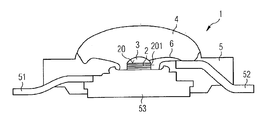
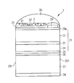
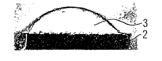
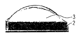
KR20170131724A - 반도체 소자 그리고 반도체 소자를 제조하기 위한 방법 - Google Patents
반도체 소자 그리고 반도체 소자를 제조하기 위한 방법 Download PDFInfo
- Publication number
- KR20170131724A KR20170131724A KR1020177033700A KR20177033700A KR20170131724A KR 20170131724 A KR20170131724 A KR 20170131724A KR 1020177033700 A KR1020177033700 A KR 1020177033700A KR 20177033700 A KR20177033700 A KR 20177033700A KR 20170131724 A KR20170131724 A KR 20170131724A
- Authority
- KR
- South Korea
- Prior art keywords
- optical element
- semiconductor chip
- molding compound
- refractive index
- semiconductor
- Prior art date
- Legal status (The legal status is an assumption and is not a legal conclusion. Google has not performed a legal analysis and makes no representation as to the accuracy of the status listed.)
- Ceased
Links
Images
Classifications
-
- H—ELECTRICITY
- H10—SEMICONDUCTOR DEVICES; ELECTRIC SOLID-STATE DEVICES NOT OTHERWISE PROVIDED FOR
- H10H—INORGANIC LIGHT-EMITTING SEMICONDUCTOR DEVICES HAVING POTENTIAL BARRIERS
- H10H20/00—Individual inorganic light-emitting semiconductor devices having potential barriers, e.g. light-emitting diodes [LED]
- H10H20/80—Constructional details
- H10H20/85—Packages
- H10H20/852—Encapsulations
-
- H01L33/52—
-
- B—PERFORMING OPERATIONS; TRANSPORTING
- B29—WORKING OF PLASTICS; WORKING OF SUBSTANCES IN A PLASTIC STATE IN GENERAL
- B29D—PRODUCING PARTICULAR ARTICLES FROM PLASTICS OR FROM SUBSTANCES IN A PLASTIC STATE
- B29D11/00—Producing optical elements, e.g. lenses or prisms
- B29D11/00009—Production of simple or compound lenses
- B29D11/00432—Auxiliary operations, e.g. machines for filling the moulds
- B29D11/00442—Curing the lens material
-
- G—PHYSICS
- G02—OPTICS
- G02B—OPTICAL ELEMENTS, SYSTEMS OR APPARATUS
- G02B1/00—Optical elements characterised by the material of which they are made; Optical coatings for optical elements
- G02B1/04—Optical elements characterised by the material of which they are made; Optical coatings for optical elements made of organic materials, e.g. plastics
-
- G—PHYSICS
- G02—OPTICS
- G02B—OPTICAL ELEMENTS, SYSTEMS OR APPARATUS
- G02B27/00—Optical systems or apparatus not provided for by any of the groups G02B1/00 - G02B26/00, G02B30/00
- G02B27/09—Beam shaping, e.g. changing the cross-sectional area, not otherwise provided for
- G02B27/0938—Using specific optical elements
- G02B27/095—Refractive optical elements
-
- H01L33/486—
-
- H01L33/50—
-
- H01L33/501—
-
- H01L33/507—
-
- H01L33/56—
-
- H01L33/58—
-
- H—ELECTRICITY
- H10—SEMICONDUCTOR DEVICES; ELECTRIC SOLID-STATE DEVICES NOT OTHERWISE PROVIDED FOR
- H10H—INORGANIC LIGHT-EMITTING SEMICONDUCTOR DEVICES HAVING POTENTIAL BARRIERS
- H10H20/00—Individual inorganic light-emitting semiconductor devices having potential barriers, e.g. light-emitting diodes [LED]
- H10H20/01—Manufacture or treatment
- H10H20/036—Manufacture or treatment of packages
- H10H20/0362—Manufacture or treatment of packages of encapsulations
-
- H—ELECTRICITY
- H10—SEMICONDUCTOR DEVICES; ELECTRIC SOLID-STATE DEVICES NOT OTHERWISE PROVIDED FOR
- H10H—INORGANIC LIGHT-EMITTING SEMICONDUCTOR DEVICES HAVING POTENTIAL BARRIERS
- H10H20/00—Individual inorganic light-emitting semiconductor devices having potential barriers, e.g. light-emitting diodes [LED]
- H10H20/80—Constructional details
- H10H20/85—Packages
- H10H20/8506—Containers
-
- H—ELECTRICITY
- H10—SEMICONDUCTOR DEVICES; ELECTRIC SOLID-STATE DEVICES NOT OTHERWISE PROVIDED FOR
- H10H—INORGANIC LIGHT-EMITTING SEMICONDUCTOR DEVICES HAVING POTENTIAL BARRIERS
- H10H20/00—Individual inorganic light-emitting semiconductor devices having potential barriers, e.g. light-emitting diodes [LED]
- H10H20/80—Constructional details
- H10H20/85—Packages
- H10H20/851—Wavelength conversion means
- H10H20/8511—Wavelength conversion means characterised by their material, e.g. binder
-
- H—ELECTRICITY
- H10—SEMICONDUCTOR DEVICES; ELECTRIC SOLID-STATE DEVICES NOT OTHERWISE PROVIDED FOR
- H10H—INORGANIC LIGHT-EMITTING SEMICONDUCTOR DEVICES HAVING POTENTIAL BARRIERS
- H10H20/00—Individual inorganic light-emitting semiconductor devices having potential barriers, e.g. light-emitting diodes [LED]
- H10H20/80—Constructional details
- H10H20/85—Packages
- H10H20/851—Wavelength conversion means
- H10H20/8515—Wavelength conversion means not being in contact with the bodies
-
- H—ELECTRICITY
- H10—SEMICONDUCTOR DEVICES; ELECTRIC SOLID-STATE DEVICES NOT OTHERWISE PROVIDED FOR
- H10H—INORGANIC LIGHT-EMITTING SEMICONDUCTOR DEVICES HAVING POTENTIAL BARRIERS
- H10H20/00—Individual inorganic light-emitting semiconductor devices having potential barriers, e.g. light-emitting diodes [LED]
- H10H20/80—Constructional details
- H10H20/85—Packages
- H10H20/852—Encapsulations
- H10H20/853—Encapsulations characterised by their shape
-
- H—ELECTRICITY
- H10—SEMICONDUCTOR DEVICES; ELECTRIC SOLID-STATE DEVICES NOT OTHERWISE PROVIDED FOR
- H10H—INORGANIC LIGHT-EMITTING SEMICONDUCTOR DEVICES HAVING POTENTIAL BARRIERS
- H10H20/00—Individual inorganic light-emitting semiconductor devices having potential barriers, e.g. light-emitting diodes [LED]
- H10H20/80—Constructional details
- H10H20/85—Packages
- H10H20/852—Encapsulations
- H10H20/854—Encapsulations characterised by their material, e.g. epoxy or silicone resins
-
- H—ELECTRICITY
- H10—SEMICONDUCTOR DEVICES; ELECTRIC SOLID-STATE DEVICES NOT OTHERWISE PROVIDED FOR
- H10H—INORGANIC LIGHT-EMITTING SEMICONDUCTOR DEVICES HAVING POTENTIAL BARRIERS
- H10H20/00—Individual inorganic light-emitting semiconductor devices having potential barriers, e.g. light-emitting diodes [LED]
- H10H20/80—Constructional details
- H10H20/85—Packages
- H10H20/855—Optical field-shaping means, e.g. lenses
-
- H—ELECTRICITY
- H01—ELECTRIC ELEMENTS
- H01L—SEMICONDUCTOR DEVICES NOT COVERED BY CLASS H10
- H01L2224/00—Indexing scheme for arrangements for connecting or disconnecting semiconductor or solid-state bodies and methods related thereto as covered by H01L24/00
- H01L2224/01—Means for bonding being attached to, or being formed on, the surface to be connected, e.g. chip-to-package, die-attach, "first-level" interconnects; Manufacturing methods related thereto
- H01L2224/26—Layer connectors, e.g. plate connectors, solder or adhesive layers; Manufacturing methods related thereto
- H01L2224/31—Structure, shape, material or disposition of the layer connectors after the connecting process
- H01L2224/32—Structure, shape, material or disposition of the layer connectors after the connecting process of an individual layer connector
- H01L2224/321—Disposition
- H01L2224/32151—Disposition the layer connector connecting between a semiconductor or solid-state body and an item not being a semiconductor or solid-state body, e.g. chip-to-substrate, chip-to-passive
- H01L2224/32221—Disposition the layer connector connecting between a semiconductor or solid-state body and an item not being a semiconductor or solid-state body, e.g. chip-to-substrate, chip-to-passive the body and the item being stacked
- H01L2224/32245—Disposition the layer connector connecting between a semiconductor or solid-state body and an item not being a semiconductor or solid-state body, e.g. chip-to-substrate, chip-to-passive the body and the item being stacked the item being metallic
-
- H—ELECTRICITY
- H01—ELECTRIC ELEMENTS
- H01L—SEMICONDUCTOR DEVICES NOT COVERED BY CLASS H10
- H01L2224/00—Indexing scheme for arrangements for connecting or disconnecting semiconductor or solid-state bodies and methods related thereto as covered by H01L24/00
- H01L2224/01—Means for bonding being attached to, or being formed on, the surface to be connected, e.g. chip-to-package, die-attach, "first-level" interconnects; Manufacturing methods related thereto
- H01L2224/42—Wire connectors; Manufacturing methods related thereto
- H01L2224/47—Structure, shape, material or disposition of the wire connectors after the connecting process
- H01L2224/48—Structure, shape, material or disposition of the wire connectors after the connecting process of an individual wire connector
- H01L2224/4805—Shape
- H01L2224/4809—Loop shape
- H01L2224/48091—Arched
-
- H—ELECTRICITY
- H01—ELECTRIC ELEMENTS
- H01L—SEMICONDUCTOR DEVICES NOT COVERED BY CLASS H10
- H01L2224/00—Indexing scheme for arrangements for connecting or disconnecting semiconductor or solid-state bodies and methods related thereto as covered by H01L24/00
- H01L2224/01—Means for bonding being attached to, or being formed on, the surface to be connected, e.g. chip-to-package, die-attach, "first-level" interconnects; Manufacturing methods related thereto
- H01L2224/42—Wire connectors; Manufacturing methods related thereto
- H01L2224/47—Structure, shape, material or disposition of the wire connectors after the connecting process
- H01L2224/48—Structure, shape, material or disposition of the wire connectors after the connecting process of an individual wire connector
- H01L2224/481—Disposition
- H01L2224/48151—Connecting between a semiconductor or solid-state body and an item not being a semiconductor or solid-state body, e.g. chip-to-substrate, chip-to-passive
- H01L2224/48221—Connecting between a semiconductor or solid-state body and an item not being a semiconductor or solid-state body, e.g. chip-to-substrate, chip-to-passive the body and the item being stacked
- H01L2224/48245—Connecting between a semiconductor or solid-state body and an item not being a semiconductor or solid-state body, e.g. chip-to-substrate, chip-to-passive the body and the item being stacked the item being metallic
- H01L2224/48247—Connecting between a semiconductor or solid-state body and an item not being a semiconductor or solid-state body, e.g. chip-to-substrate, chip-to-passive the body and the item being stacked the item being metallic connecting the wire to a bond pad of the item
-
- H—ELECTRICITY
- H01—ELECTRIC ELEMENTS
- H01L—SEMICONDUCTOR DEVICES NOT COVERED BY CLASS H10
- H01L2224/00—Indexing scheme for arrangements for connecting or disconnecting semiconductor or solid-state bodies and methods related thereto as covered by H01L24/00
- H01L2224/73—Means for bonding being of different types provided for in two or more of groups H01L2224/10, H01L2224/18, H01L2224/26, H01L2224/34, H01L2224/42, H01L2224/50, H01L2224/63, H01L2224/71
- H01L2224/732—Location after the connecting process
- H01L2224/73251—Location after the connecting process on different surfaces
- H01L2224/73265—Layer and wire connectors
-
- H—ELECTRICITY
- H01—ELECTRIC ELEMENTS
- H01L—SEMICONDUCTOR DEVICES NOT COVERED BY CLASS H10
- H01L2224/00—Indexing scheme for arrangements for connecting or disconnecting semiconductor or solid-state bodies and methods related thereto as covered by H01L24/00
- H01L2224/80—Methods for connecting semiconductor or other solid state bodies using means for bonding being attached to, or being formed on, the surface to be connected
- H01L2224/85—Methods for connecting semiconductor or other solid state bodies using means for bonding being attached to, or being formed on, the surface to be connected using a wire connector
- H01L2224/85909—Post-treatment of the connector or wire bonding area
- H01L2224/8592—Applying permanent coating, e.g. protective coating
-
- H01L2933/005—
-
- H—ELECTRICITY
- H10—SEMICONDUCTOR DEVICES; ELECTRIC SOLID-STATE DEVICES NOT OTHERWISE PROVIDED FOR
- H10H—INORGANIC LIGHT-EMITTING SEMICONDUCTOR DEVICES HAVING POTENTIAL BARRIERS
- H10H20/00—Individual inorganic light-emitting semiconductor devices having potential barriers, e.g. light-emitting diodes [LED]
- H10H20/01—Manufacture or treatment
- H10H20/036—Manufacture or treatment of packages
- H10H20/0363—Manufacture or treatment of packages of optical field-shaping means
-
- H—ELECTRICITY
- H10—SEMICONDUCTOR DEVICES; ELECTRIC SOLID-STATE DEVICES NOT OTHERWISE PROVIDED FOR
- H10H—INORGANIC LIGHT-EMITTING SEMICONDUCTOR DEVICES HAVING POTENTIAL BARRIERS
- H10H20/00—Individual inorganic light-emitting semiconductor devices having potential barriers, e.g. light-emitting diodes [LED]
- H10H20/80—Constructional details
- H10H20/85—Packages
- H10H20/857—Interconnections, e.g. lead-frames, bond wires or solder balls
Landscapes
- Physics & Mathematics (AREA)
- Engineering & Computer Science (AREA)
- Optics & Photonics (AREA)
- General Physics & Mathematics (AREA)
- Health & Medical Sciences (AREA)
- Ophthalmology & Optometry (AREA)
- Mechanical Engineering (AREA)
- Manufacturing & Machinery (AREA)
- Led Device Packages (AREA)
- Chemical & Material Sciences (AREA)
- Chemical Kinetics & Catalysis (AREA)
- Medicinal Chemistry (AREA)
- Polymers & Plastics (AREA)
- Organic Chemistry (AREA)
Applications Claiming Priority (3)
| Application Number | Priority Date | Filing Date | Title |
|---|---|---|---|
| DE102010024545.3A DE102010024545B4 (de) | 2010-06-22 | 2010-06-22 | Halbleiterbauelement und Verfahren zur Herstellung eines Halbleiterbauelements |
| DE102010024545.3 | 2010-06-22 | ||
| PCT/EP2011/058580 WO2011160913A1 (de) | 2010-06-22 | 2011-05-25 | Halbleiterbauelement und verfahren zur herstellung eines halbleiterbauelements |
Related Parent Applications (1)
| Application Number | Title | Priority Date | Filing Date |
|---|---|---|---|
| KR1020137001259A Division KR20130023347A (ko) | 2010-06-22 | 2011-05-25 | 반도체 소자 그리고 반도체 소자를 제조하기 위한 방법 |
Publications (1)
| Publication Number | Publication Date |
|---|---|
| KR20170131724A true KR20170131724A (ko) | 2017-11-29 |
Family
ID=44260354
Family Applications (2)
| Application Number | Title | Priority Date | Filing Date |
|---|---|---|---|
| KR1020177033700A Ceased KR20170131724A (ko) | 2010-06-22 | 2011-05-25 | 반도체 소자 그리고 반도체 소자를 제조하기 위한 방법 |
| KR1020137001259A Ceased KR20130023347A (ko) | 2010-06-22 | 2011-05-25 | 반도체 소자 그리고 반도체 소자를 제조하기 위한 방법 |
Family Applications After (1)
| Application Number | Title | Priority Date | Filing Date |
|---|---|---|---|
| KR1020137001259A Ceased KR20130023347A (ko) | 2010-06-22 | 2011-05-25 | 반도체 소자 그리고 반도체 소자를 제조하기 위한 방법 |
Country Status (8)
| Country | Link |
|---|---|
| US (2) | US9368699B2 (enExample) |
| EP (1) | EP2586069B1 (enExample) |
| JP (1) | JP6315988B2 (enExample) |
| KR (2) | KR20170131724A (enExample) |
| CN (2) | CN102947959B (enExample) |
| DE (1) | DE102010024545B4 (enExample) |
| TW (2) | TWI545809B (enExample) |
| WO (1) | WO2011160913A1 (enExample) |
Families Citing this family (2)
| Publication number | Priority date | Publication date | Assignee | Title |
|---|---|---|---|---|
| DE102010024545B4 (de) | 2010-06-22 | 2022-01-13 | OSRAM Opto Semiconductors Gesellschaft mit beschränkter Haftung | Halbleiterbauelement und Verfahren zur Herstellung eines Halbleiterbauelements |
| DE102014108368A1 (de) * | 2014-06-13 | 2015-12-17 | Osram Opto Semiconductors Gmbh | Oberflächenmontierbares Halbleiterbauelement und Verfahren zu dessen Herstellung |
Family Cites Families (24)
| Publication number | Priority date | Publication date | Assignee | Title |
|---|---|---|---|---|
| JPS6159406A (ja) * | 1984-08-31 | 1986-03-26 | Fujitsu Ltd | プレ−ナ型光ガイドの光結合構造およびその製造方法 |
| DE10023353A1 (de) | 2000-05-12 | 2001-11-29 | Osram Opto Semiconductors Gmbh | Optoelektronisches Bauelement und Verfahren zur Herstellung |
| JP3991612B2 (ja) | 2001-04-09 | 2007-10-17 | 日亜化学工業株式会社 | 発光素子 |
| DE10129785B4 (de) * | 2001-06-20 | 2010-03-18 | Osram Opto Semiconductors Gmbh | Optoelektronisches Bauelement und Verfahren zu seiner Herstellung |
| JP2003224304A (ja) | 2002-01-28 | 2003-08-08 | Kasei Optonix Co Ltd | 発光装置 |
| JP4241259B2 (ja) * | 2003-08-06 | 2009-03-18 | セイコーエプソン株式会社 | マイクロレンズの製造方法 |
| DE10361650A1 (de) | 2003-12-30 | 2005-08-04 | Osram Opto Semiconductors Gmbh | Optoelektronisches Modul und Verfahren zu dessen Herstellung |
| US7645397B2 (en) | 2004-01-15 | 2010-01-12 | Nanosys, Inc. | Nanocrystal doped matrixes |
| DE102005009066A1 (de) * | 2005-02-28 | 2006-09-07 | Osram Opto Semiconductors Gmbh | Verfahren zur Herstellung eines optischen und eines strahlungsemittierenden Bauelementes und optisches sowie strahlungsemittierendes Bauelement |
| RU2401846C2 (ru) | 2006-04-25 | 2010-10-20 | Учреждение Российской академии наук Институт синтетических полимерных материалов им. Н.С. Ениколопова РАН (ИСПМ РАН) | Функциональные полиорганосилоксаны и композиция, способная к отверждению на их основе |
| TWI338380B (en) | 2006-10-11 | 2011-03-01 | Chuan Yu Hung | Light emitting diode incorporating high refractive index material |
| KR20090089431A (ko) * | 2006-11-17 | 2009-08-21 | 쓰리엠 이노베이티브 프로퍼티즈 컴파니 | Led 광원용 광학 접합 조성물 |
| US8029904B2 (en) * | 2006-12-01 | 2011-10-04 | Rohm And Haas Company | Aryl (thio)ether aryl polysiloxane composition and methods for making and using same |
| US8895652B2 (en) | 2007-06-12 | 2014-11-25 | Ajjer, Llc | High refractive index materials and composites |
| JP5318383B2 (ja) * | 2007-08-07 | 2013-10-16 | デクセリアルズ株式会社 | 光学部品封止材及び発光装置 |
| TW200910648A (en) * | 2007-08-31 | 2009-03-01 | Isotech Products Inc | Forming process of resin lens of an LED component |
| JP5578597B2 (ja) * | 2007-09-03 | 2014-08-27 | 独立行政法人物質・材料研究機構 | 蛍光体及びその製造方法、並びにそれを用いた発光装置 |
| US20090065792A1 (en) * | 2007-09-07 | 2009-03-12 | 3M Innovative Properties Company | Method of making an led device having a dome lens |
| US10256385B2 (en) * | 2007-10-31 | 2019-04-09 | Cree, Inc. | Light emitting die (LED) packages and related methods |
| US8866169B2 (en) * | 2007-10-31 | 2014-10-21 | Cree, Inc. | LED package with increased feature sizes |
| US9287469B2 (en) | 2008-05-02 | 2016-03-15 | Cree, Inc. | Encapsulation for phosphor-converted white light emitting diode |
| JP2009275196A (ja) | 2008-05-19 | 2009-11-26 | Sony Corp | 硬化性樹脂材料組成物、光学材料、発光装置及びその製造方法、並びに電子デバイス |
| CN101740707B (zh) * | 2009-12-11 | 2013-11-06 | 晶科电子(广州)有限公司 | 预成型荧光粉贴片及其与发光二极管的封装方法 |
| DE102010024545B4 (de) | 2010-06-22 | 2022-01-13 | OSRAM Opto Semiconductors Gesellschaft mit beschränkter Haftung | Halbleiterbauelement und Verfahren zur Herstellung eines Halbleiterbauelements |
-
2010
- 2010-06-22 DE DE102010024545.3A patent/DE102010024545B4/de active Active
-
2011
- 2011-05-25 WO PCT/EP2011/058580 patent/WO2011160913A1/de not_active Ceased
- 2011-05-25 JP JP2013515795A patent/JP6315988B2/ja not_active Expired - Fee Related
- 2011-05-25 KR KR1020177033700A patent/KR20170131724A/ko not_active Ceased
- 2011-05-25 CN CN201180031248.9A patent/CN102947959B/zh active Active
- 2011-05-25 EP EP11723914.5A patent/EP2586069B1/de active Active
- 2011-05-25 KR KR1020137001259A patent/KR20130023347A/ko not_active Ceased
- 2011-05-25 CN CN201610015092.XA patent/CN105529392B/zh active Active
- 2011-05-25 US US13/703,180 patent/US9368699B2/en active Active
- 2011-06-20 TW TW104124265A patent/TWI545809B/zh active
- 2011-06-20 TW TW100121392A patent/TWI497776B/zh active
-
2016
- 2016-05-05 US US15/146,984 patent/US9634207B2/en active Active
Also Published As
| Publication number | Publication date |
|---|---|
| KR20130023347A (ko) | 2013-03-07 |
| TWI545809B (zh) | 2016-08-11 |
| CN105529392B (zh) | 2019-10-18 |
| EP2586069A1 (de) | 2013-05-01 |
| CN102947959A (zh) | 2013-02-27 |
| US20160247986A1 (en) | 2016-08-25 |
| US9368699B2 (en) | 2016-06-14 |
| JP2013534728A (ja) | 2013-09-05 |
| US20130240929A1 (en) | 2013-09-19 |
| DE102010024545B4 (de) | 2022-01-13 |
| TW201541673A (zh) | 2015-11-01 |
| JP6315988B2 (ja) | 2018-04-25 |
| TWI497776B (zh) | 2015-08-21 |
| WO2011160913A1 (de) | 2011-12-29 |
| US9634207B2 (en) | 2017-04-25 |
| EP2586069B1 (de) | 2017-03-01 |
| CN102947959B (zh) | 2016-01-27 |
| TW201208148A (en) | 2012-02-16 |
| CN105529392A (zh) | 2016-04-27 |
| DE102010024545A1 (de) | 2011-12-22 |
Similar Documents
| Publication | Publication Date | Title |
|---|---|---|
| TW569473B (en) | Opto-electronic component | |
| US10217915B2 (en) | Optoelectronic semiconductor component | |
| US8860062B2 (en) | Optoelectronic semiconductor component | |
| JP4922189B2 (ja) | 光学素子及び放射線を発する素子の製造方法及び光学素子ならびに放射線を発する素子 | |
| EP3154095B1 (en) | Light emitting device with beveled reflector and manufacturing method of the same | |
| KR101862818B1 (ko) | 광전자 컴포넌트 및 광전자 컴포넌트를 제조하기 위한 방법 | |
| KR101759263B1 (ko) | 광전자 소자 그리고 광전자 소자 및 복합 구조물을 제조하기 위한 방법 | |
| US20130207144A1 (en) | Component and method for producing a component | |
| KR20100016491A (ko) | 광전 소자 | |
| JP2012529766A (ja) | 遠隔の蛍燐光体の層及び反射性のサブマウントを備えたled | |
| WO2011027240A1 (en) | Led package with phosphor plate and reflective substrate | |
| CN1754268A (zh) | 照明模块及其制造方法 | |
| US20130228810A1 (en) | Solid state lighting luminaire and a fabrication method thereof | |
| CN102460745A (zh) | 光电子半导体器件 | |
| US10615323B2 (en) | Component having a reflector and method of producing components | |
| US7893452B2 (en) | Optoelectronic component and package for an optoelectronic component | |
| US9634207B2 (en) | Semiconductor component and method of producing a semiconductor component | |
| KR20130102117A (ko) | 복합 기판, 복합 기판을 포함하는 반도체 칩 및, 복합 기판과 반도체 칩의 제조 방법 | |
| US11824143B2 (en) | Optoelectronic component, method for producing an optoelectronic component and lighting device | |
| KR102555812B1 (ko) | 발광 장치 | |
| KR101223051B1 (ko) | 엘이디 패키지 | |
| KR20130025482A (ko) | 발광 소자 패키지 |
Legal Events
| Date | Code | Title | Description |
|---|---|---|---|
| A107 | Divisional application of patent | ||
| A201 | Request for examination | ||
| PA0104 | Divisional application for international application |
Comment text: Divisional Application for International Patent Patent event code: PA01041R01D Patent event date: 20171121 Application number text: 1020137001259 Filing date: 20130117 |
|
| PA0201 | Request for examination | ||
| PG1501 | Laying open of application | ||
| E902 | Notification of reason for refusal | ||
| PE0902 | Notice of grounds for rejection |
Comment text: Notification of reason for refusal Patent event date: 20171211 Patent event code: PE09021S01D |
|
| AMND | Amendment | ||
| E601 | Decision to refuse application | ||
| PE0601 | Decision on rejection of patent |
Patent event date: 20180312 Comment text: Decision to Refuse Application Patent event code: PE06012S01D Patent event date: 20171211 Comment text: Notification of reason for refusal Patent event code: PE06011S01I |
|
| AMND | Amendment | ||
| PX0901 | Re-examination |
Patent event code: PX09011S01I Patent event date: 20180312 Comment text: Decision to Refuse Application Patent event code: PX09012R01I Patent event date: 20180209 Comment text: Amendment to Specification, etc. |
|
| PX0601 | Decision of rejection after re-examination |
Comment text: Decision to Refuse Application Patent event code: PX06014S01D Patent event date: 20180625 Comment text: Amendment to Specification, etc. Patent event code: PX06012R01I Patent event date: 20180611 Comment text: Decision to Refuse Application Patent event code: PX06011S01I Patent event date: 20180312 Comment text: Amendment to Specification, etc. Patent event code: PX06012R01I Patent event date: 20180209 Comment text: Notification of reason for refusal Patent event code: PX06013S01I Patent event date: 20171211 |
