KR20170116632A - 플렉서블 디스플레이 장치 - Google Patents
플렉서블 디스플레이 장치 Download PDFInfo
- Publication number
- KR20170116632A KR20170116632A KR1020160044260A KR20160044260A KR20170116632A KR 20170116632 A KR20170116632 A KR 20170116632A KR 1020160044260 A KR1020160044260 A KR 1020160044260A KR 20160044260 A KR20160044260 A KR 20160044260A KR 20170116632 A KR20170116632 A KR 20170116632A
- Authority
- KR
- South Korea
- Prior art keywords
- light emitting
- flexible substrate
- disposed
- layer
- emitting diodes
- Prior art date
- Legal status (The legal status is an assumption and is not a legal conclusion. Google has not performed a legal analysis and makes no representation as to the accuracy of the status listed.)
- Granted
Links
Images

Classifications
-
- H—ELECTRICITY
- H10—SEMICONDUCTOR DEVICES; ELECTRIC SOLID-STATE DEVICES NOT OTHERWISE PROVIDED FOR
- H10W—GENERIC PACKAGES, INTERCONNECTIONS, CONNECTORS OR OTHER CONSTRUCTIONAL DETAILS OF DEVICES COVERED BY CLASS H10
- H10W90/00—Package configurations
-
- H—ELECTRICITY
- H10—SEMICONDUCTOR DEVICES; ELECTRIC SOLID-STATE DEVICES NOT OTHERWISE PROVIDED FOR
- H10K—ORGANIC ELECTRIC SOLID-STATE DEVICES
- H10K77/00—Constructional details of devices covered by this subclass and not covered by groups H10K10/80, H10K30/80, H10K50/80 or H10K59/80
- H10K77/10—Substrates, e.g. flexible substrates
- H10K77/111—Flexible substrates
-
- H01L51/0097—
-
- G—PHYSICS
- G06—COMPUTING OR CALCULATING; COUNTING
- G06F—ELECTRIC DIGITAL DATA PROCESSING
- G06F1/00—Details not covered by groups G06F3/00 - G06F13/00 and G06F21/00
- G06F1/16—Constructional details or arrangements
- G06F1/1613—Constructional details or arrangements for portable computers
- G06F1/1633—Constructional details or arrangements of portable computers not specific to the type of enclosures covered by groups G06F1/1615 - G06F1/1626
- G06F1/1637—Details related to the display arrangement, including those related to the mounting of the display in the housing
- G06F1/1652—Details related to the display arrangement, including those related to the mounting of the display in the housing the display being flexible, e.g. mimicking a sheet of paper, or rollable
-
- G—PHYSICS
- G09—EDUCATION; CRYPTOGRAPHY; DISPLAY; ADVERTISING; SEALS
- G09F—DISPLAYING; ADVERTISING; SIGNS; LABELS OR NAME-PLATES; SEALS
- G09F9/00—Indicating arrangements for variable information in which the information is built-up on a support by selection or combination of individual elements
- G09F9/30—Indicating arrangements for variable information in which the information is built-up on a support by selection or combination of individual elements in which the desired character or characters are formed by combining individual elements
- G09F9/301—Indicating arrangements for variable information in which the information is built-up on a support by selection or combination of individual elements in which the desired character or characters are formed by combining individual elements flexible foldable or roll-able electronic displays, e.g. thin LCD, OLED
-
- H01L31/03926—
-
- H—ELECTRICITY
- H10—SEMICONDUCTOR DEVICES; ELECTRIC SOLID-STATE DEVICES NOT OTHERWISE PROVIDED FOR
- H10D—INORGANIC ELECTRIC SEMICONDUCTOR DEVICES
- H10D86/00—Integrated devices formed in or on insulating or conducting substrates, e.g. formed in silicon-on-insulator [SOI] substrates or on stainless steel or glass substrates
- H10D86/40—Integrated devices formed in or on insulating or conducting substrates, e.g. formed in silicon-on-insulator [SOI] substrates or on stainless steel or glass substrates characterised by multiple TFTs
- H10D86/411—Integrated devices formed in or on insulating or conducting substrates, e.g. formed in silicon-on-insulator [SOI] substrates or on stainless steel or glass substrates characterised by multiple TFTs characterised by materials, geometry or structure of the substrates
-
- H—ELECTRICITY
- H10—SEMICONDUCTOR DEVICES; ELECTRIC SOLID-STATE DEVICES NOT OTHERWISE PROVIDED FOR
- H10D—INORGANIC ELECTRIC SEMICONDUCTOR DEVICES
- H10D86/00—Integrated devices formed in or on insulating or conducting substrates, e.g. formed in silicon-on-insulator [SOI] substrates or on stainless steel or glass substrates
- H10D86/40—Integrated devices formed in or on insulating or conducting substrates, e.g. formed in silicon-on-insulator [SOI] substrates or on stainless steel or glass substrates characterised by multiple TFTs
- H10D86/60—Integrated devices formed in or on insulating or conducting substrates, e.g. formed in silicon-on-insulator [SOI] substrates or on stainless steel or glass substrates characterised by multiple TFTs wherein the TFTs are in active matrices
-
- H—ELECTRICITY
- H10—SEMICONDUCTOR DEVICES; ELECTRIC SOLID-STATE DEVICES NOT OTHERWISE PROVIDED FOR
- H10F—INORGANIC SEMICONDUCTOR DEVICES SENSITIVE TO INFRARED RADIATION, LIGHT, ELECTROMAGNETIC RADIATION OF SHORTER WAVELENGTH OR CORPUSCULAR RADIATION
- H10F77/00—Constructional details of devices covered by this subclass
- H10F77/10—Semiconductor bodies
- H10F77/16—Material structures, e.g. crystalline structures, film structures or crystal plane orientations
- H10F77/169—Thin semiconductor films on metallic or insulating substrates
- H10F77/1698—Thin semiconductor films on metallic or insulating substrates the metallic or insulating substrates being flexible
-
- H—ELECTRICITY
- H10—SEMICONDUCTOR DEVICES; ELECTRIC SOLID-STATE DEVICES NOT OTHERWISE PROVIDED FOR
- H10K—ORGANIC ELECTRIC SOLID-STATE DEVICES
- H10K59/00—Integrated devices, or assemblies of multiple devices, comprising at least one organic light-emitting element covered by group H10K50/00
- H10K59/10—OLED displays
- H10K59/12—Active-matrix OLED [AMOLED] displays
- H10K59/121—Active-matrix OLED [AMOLED] displays characterised by the geometry or disposition of pixel elements
-
- H—ELECTRICITY
- H10—SEMICONDUCTOR DEVICES; ELECTRIC SOLID-STATE DEVICES NOT OTHERWISE PROVIDED FOR
- H10K—ORGANIC ELECTRIC SOLID-STATE DEVICES
- H10K19/00—Integrated devices, or assemblies of multiple devices, comprising at least one organic element specially adapted for rectifying, amplifying, oscillating or switching, covered by group H10K10/00
- H10K19/20—Integrated devices, or assemblies of multiple devices, comprising at least one organic element specially adapted for rectifying, amplifying, oscillating or switching, covered by group H10K10/00 comprising components having an active region that includes an inorganic semiconductor
-
- H—ELECTRICITY
- H10—SEMICONDUCTOR DEVICES; ELECTRIC SOLID-STATE DEVICES NOT OTHERWISE PROVIDED FOR
- H10K—ORGANIC ELECTRIC SOLID-STATE DEVICES
- H10K2102/00—Constructional details relating to the organic devices covered by this subclass
- H10K2102/301—Details of OLEDs
- H10K2102/311—Flexible OLED
-
- H—ELECTRICITY
- H10—SEMICONDUCTOR DEVICES; ELECTRIC SOLID-STATE DEVICES NOT OTHERWISE PROVIDED FOR
- H10K—ORGANIC ELECTRIC SOLID-STATE DEVICES
- H10K59/00—Integrated devices, or assemblies of multiple devices, comprising at least one organic light-emitting element covered by group H10K50/00
- H10K59/80—Constructional details
- H10K59/87—Passivation; Containers; Encapsulations
- H10K59/873—Encapsulations
-
- H—ELECTRICITY
- H10—SEMICONDUCTOR DEVICES; ELECTRIC SOLID-STATE DEVICES NOT OTHERWISE PROVIDED FOR
- H10K—ORGANIC ELECTRIC SOLID-STATE DEVICES
- H10K59/00—Integrated devices, or assemblies of multiple devices, comprising at least one organic light-emitting element covered by group H10K50/00
- H10K59/80—Constructional details
- H10K59/875—Arrangements for extracting light from the devices
- H10K59/879—Arrangements for extracting light from the devices comprising refractive means, e.g. lenses
-
- Y—GENERAL TAGGING OF NEW TECHNOLOGICAL DEVELOPMENTS; GENERAL TAGGING OF CROSS-SECTIONAL TECHNOLOGIES SPANNING OVER SEVERAL SECTIONS OF THE IPC; TECHNICAL SUBJECTS COVERED BY FORMER USPC CROSS-REFERENCE ART COLLECTIONS [XRACs] AND DIGESTS
- Y02—TECHNOLOGIES OR APPLICATIONS FOR MITIGATION OR ADAPTATION AGAINST CLIMATE CHANGE
- Y02E—REDUCTION OF GREENHOUSE GAS [GHG] EMISSIONS, RELATED TO ENERGY GENERATION, TRANSMISSION OR DISTRIBUTION
- Y02E10/00—Energy generation through renewable energy sources
- Y02E10/50—Photovoltaic [PV] energy
- Y02E10/549—Organic PV cells
Landscapes
- Engineering & Computer Science (AREA)
- Physics & Mathematics (AREA)
- Theoretical Computer Science (AREA)
- General Physics & Mathematics (AREA)
- Computer Hardware Design (AREA)
- Geometry (AREA)
- Microelectronics & Electronic Packaging (AREA)
- Human Computer Interaction (AREA)
- General Engineering & Computer Science (AREA)
- Electroluminescent Light Sources (AREA)
- Devices For Indicating Variable Information By Combining Individual Elements (AREA)
Abstract
Description
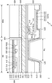
도 2는 도 1에 도시된 플렉서블 디스플레이 장치의 Ⅱ-Ⅱ 선을 따라 취한 단면을 개략적으로 도시하는 단면도이다.
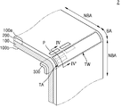
도 3은 본 발명의 일 실시예에 따른 플렉서블 디스플레이 장치를 개략적으로 도시하는 사시도이다.
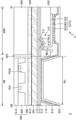
도 4는 도 3에 도시된 플렉서블 디스플레이 장치의 Ⅳ-Ⅳ 선을 따라 취한 단면을 개략적으로 도시하는 단면도이다.
100, 310: 플렉서블 기판
100a: 일면
100b: 타면
200: 제1 디스플레이부
217: 평탄화막
219: 화소정의막
220: 화소전극
230: 중간층
240: 대향전극
250: 박막봉지층
300: 제2 디스플레이부
330: 제1 절연막
330a: 오목부
340: 제2 절연막
350: 발광 다이오드
400: 보호필름
510, 520: 접착층
530: 홈
OP1: 제1 개구부
OP2: 제2 개구부
Claims (16)
- 일면 및 일면과 반대되는 타면을 갖는, 플렉서블 기판;
상기 플렉서블 기판의 상기 일면 상에 배치되며 광을 투과시키는 투광부를 갖는, 제1 디스플레이부; 및
상기 투광부에 대응하도록 상기 플렉서블 기판의 상기 타면 상에 배치되는 제2 디스플레이부;
를 구비하는, 플렉서블 디스플레이 장치. - 제1항에 있어서,
상기 플렉서블 기판은 벤딩 영역 및 비벤딩 영역을 가지며, 상기 제1 디스플레이부의 상기 투광부는 상기 플렉서블 기판의 상기 벤딩 영역에 대응하여 위치하는, 플렉서블 디스플레이 장치. - 제1항에 있어서,
상기 제1 디스플레이부는 복수개의 화소전극들, 상기 복수개의 화소전극들에 대향하는 대향전극 및 상기 복수개의 화소전극들과 상기 대향전극 사이에 개재되는 유기발광층을 각각 포함하는 복수개의 중간층들을 구비하는 복수개의 유기발광소자(OLED)들을 포함하는, 플렉서블 디스플레이 장치. - 제3항에 있어서,
상기 제2 디스플레이부는 복수개의 발광 다이오드(LED)들을 포함하는, 플렉서블 디스플레이 장치. - 제4항에 있어서,
상기 복수개의 유기발광소자(OLED)들은 일 방향을 따라 제1 간격으로 이격되어 배치되고, 상기 복수개의 발광 다이오드(LED)들은 일 방향을 따라 상기 제1 간격과 동일한 제2 간격으로 이격되어 배치되는, 플렉서블 디스플레이 장치. - 제4항에 있어서,
상기 복수개의 유기발광소자(OLED)들은 일 방향을 따라 제1 간격으로 이격되어 배치되고, 상기 복수개의 발광 다이오드(LED)들은 일 방향을 따라 상기 제1 간격과 상이한 제2 간격으로 이격되어 배치되는, 플렉서블 디스플레이 장치. - 제4항에 있어서,
상기 복수개의 발광 다이오드(LED)들 각각은 p-n다이오드를 포함하는, 플렉서블 디스플레이 장치. - 제4항에 있어서,
상기 복수개의 발광 다이오드(LED)들 각각은 1 um 내지 100 um인, 플렉서블 디스플레이 장치. - 제4항에 있어서,
상기 복수개의 발광 다이오드(LED)들에서 발광한 빛은 상기 제1 디스플레이부가 위치한 방향으로 발광하는, 플렉서블 디스플레이 장치. - 제4항에 있어서,
상기 복수개의 발광 다이오드(LED)들 각각은 수평 발광형 발광 다이오드인, 플렉서블 디스플레이 장치. - 제4항에 있어서,
상기 투광부는 복수개의 절연층들을 포함하고, 상기 복수개의 절연층들 중 적어도 한층은 적어도 하나의 제1 개구부를 갖는, 플렉서블 디스플레이 장치. - 제11항에 있어서,
상기 복수개의 발광 다이오드(LED)들은 상기 제1 개구부에 대응하도록 배치되는, 플렉서블 디스플레이 장치. - 제11항에 있어서,
상기 제1 디스플레이부는 비벤딩 영역 상에 화소영역을 정의하는 제2 개구부를 갖고, 상기 제1 개구부와 상기 제2 개구부의 면적은 동일한, 플렉서블 디스플레이 장치. - 제1항에 있어서,
상기 플렉서블 기판의 상기 타면 상에 배치되는 보호필름을 더 포함하는, 플렉서블 디스플레이 장치. - 제14항에 있어서,
상기 보호필름은 상기 플렉서블 기판의 상기 타면 중 상기 제2 디스플레이부가 배치된 부분을 제외하고 배치되는, 플렉서블 디스플레이 장치. - 제1항에 있어서,
상기 플렉서블 기판의 타면과 상기 제2 디스플레이부 사이에 개재되는 투광성의 접착층을 더 포함하는, 플렉서블 디스플레이 장치.
Priority Applications (2)
| Application Number | Priority Date | Filing Date | Title |
|---|---|---|---|
| KR1020160044260A KR102547686B1 (ko) | 2016-04-11 | 2016-04-11 | 플렉서블 디스플레이 장치 |
| US15/484,202 US10242975B2 (en) | 2016-04-11 | 2017-04-11 | Flexible display apparatus |
Applications Claiming Priority (1)
| Application Number | Priority Date | Filing Date | Title |
|---|---|---|---|
| KR1020160044260A KR102547686B1 (ko) | 2016-04-11 | 2016-04-11 | 플렉서블 디스플레이 장치 |
Publications (2)
| Publication Number | Publication Date |
|---|---|
| KR20170116632A true KR20170116632A (ko) | 2017-10-20 |
| KR102547686B1 KR102547686B1 (ko) | 2023-06-27 |
Family
ID=59998864
Family Applications (1)
| Application Number | Title | Priority Date | Filing Date |
|---|---|---|---|
| KR1020160044260A Active KR102547686B1 (ko) | 2016-04-11 | 2016-04-11 | 플렉서블 디스플레이 장치 |
Country Status (2)
| Country | Link |
|---|---|
| US (1) | US10242975B2 (ko) |
| KR (1) | KR102547686B1 (ko) |
Cited By (6)
| Publication number | Priority date | Publication date | Assignee | Title |
|---|---|---|---|---|
| US11081670B2 (en) | 2019-03-07 | 2021-08-03 | Samsung Display Co., Ltd. | Display device |
| US11081538B2 (en) | 2018-07-03 | 2021-08-03 | Samsung Display Co., Ltd. | Organic light emitting diode display device having a circuit structure buried in a substrate thereof |
| TWI753715B (zh) * | 2020-08-24 | 2022-01-21 | 錼創顯示科技股份有限公司 | 顯示裝置 |
| US11495149B2 (en) | 2020-08-24 | 2022-11-08 | PlayNitride Display Co., Ltd. | Display apparatus |
| WO2023171898A1 (ko) * | 2022-03-08 | 2023-09-14 | 삼성디스플레이 주식회사 | 표시 장치 및 그것의 제조 방법 |
| US11782479B2 (en) | 2020-02-13 | 2023-10-10 | Samsung Display Co., Ltd. | Electronic apparatus and method of manufacturing the same |
Families Citing this family (21)
| Publication number | Priority date | Publication date | Assignee | Title |
|---|---|---|---|---|
| KR102610028B1 (ko) * | 2016-04-12 | 2023-12-06 | 삼성디스플레이 주식회사 | 디스플레이 장치 |
| KR102716709B1 (ko) * | 2016-10-17 | 2024-10-14 | 삼성디스플레이 주식회사 | 표시 장치 및 그 제조 방법 |
| JP2019032456A (ja) * | 2017-08-09 | 2019-02-28 | 株式会社ジャパンディスプレイ | 押圧センサを備える表示装置 |
| CN110134182A (zh) * | 2018-02-08 | 2019-08-16 | 深圳富泰宏精密工业有限公司 | 便携式电子装置及其操作方法 |
| CN110416393B (zh) * | 2018-04-27 | 2021-10-08 | 群创光电股份有限公司 | 电子装置 |
| EP3588478B1 (en) * | 2018-06-29 | 2022-03-23 | GIO Optoelectronics Corp. | Electronic device |
| CN108987426B (zh) | 2018-07-23 | 2020-09-29 | 上海天马微电子有限公司 | 一种柔性led显示面板及电子设备 |
| CN109037239B (zh) | 2018-07-26 | 2020-11-17 | 上海天马微电子有限公司 | 一种阵列基板及其制备方法、显示面板 |
| KR102538829B1 (ko) * | 2018-09-18 | 2023-06-02 | 삼성디스플레이 주식회사 | 전자 장치 |
| CN109461742B (zh) * | 2018-10-11 | 2020-11-24 | 武汉华星光电半导体显示技术有限公司 | 一种柔性显示面板 |
| CN110010638B (zh) * | 2018-10-11 | 2021-02-02 | 京东方科技集团股份有限公司 | 显示基板及其制备方法、显示装置 |
| CN109411522A (zh) * | 2018-11-06 | 2019-03-01 | 京东方科技集团股份有限公司 | 一种透明显示面板及其制备方法、显示装置 |
| US12101426B1 (en) * | 2018-11-13 | 2024-09-24 | Apple Inc. | Electronic devices having vertical image transport layers |
| KR102661467B1 (ko) | 2018-11-26 | 2024-04-29 | 삼성디스플레이 주식회사 | 디스플레이 장치 및 이의 제조 방법 |
| CN109585511A (zh) * | 2018-12-03 | 2019-04-05 | 武汉华星光电半导体显示技术有限公司 | 显示面板及其制造方法 |
| US10950809B2 (en) * | 2018-12-21 | 2021-03-16 | Wuhan China Star Optoelectronics Semiconductor Display Technology Co., Ltd. | Flexible display panel having a photoresist supporting element |
| KR102701975B1 (ko) * | 2018-12-31 | 2024-09-02 | 엘지디스플레이 주식회사 | 유기 발광 패널 및 무기 발광 다이오드를 포함하는 조명장치 |
| CN109887956B (zh) * | 2019-01-25 | 2021-04-27 | 武汉华星光电半导体显示技术有限公司 | 有机发光二极管柔性阵列基板 |
| US11574571B2 (en) * | 2019-03-26 | 2023-02-07 | Sharp Kabushiki Kaisha | Display device having switching signal line between display regions |
| KR20210142808A (ko) * | 2020-05-18 | 2021-11-26 | 삼성디스플레이 주식회사 | 표시 장치 및 표시 장치의 제조방법 |
| EP3933931A1 (en) | 2020-07-02 | 2022-01-05 | LG Display Co., Ltd. | Display panel and method of fabricating the same |
Citations (1)
| Publication number | Priority date | Publication date | Assignee | Title |
|---|---|---|---|---|
| KR20150069379A (ko) * | 2013-12-13 | 2015-06-23 | 삼성디스플레이 주식회사 | 플렉서블 표시장치 |
Family Cites Families (6)
| Publication number | Priority date | Publication date | Assignee | Title |
|---|---|---|---|---|
| JP5097057B2 (ja) * | 2008-08-29 | 2012-12-12 | 株式会社沖データ | 表示装置 |
| KR20110054464A (ko) * | 2009-11-17 | 2011-05-25 | 삼성모바일디스플레이주식회사 | 표시 장치 |
| US8723824B2 (en) | 2011-09-27 | 2014-05-13 | Apple Inc. | Electronic devices with sidewall displays |
| US10245776B2 (en) | 2011-09-30 | 2019-04-02 | Apple Inc. | Methods for forming electronic devices with bent display edges |
| KR102283456B1 (ko) | 2013-12-18 | 2021-07-30 | 삼성디스플레이 주식회사 | 광투과율 제어가 가능한 표시 장치 |
| US10739882B2 (en) * | 2014-08-06 | 2020-08-11 | Apple Inc. | Electronic device display with array of discrete light-emitting diodes |
-
2016
- 2016-04-11 KR KR1020160044260A patent/KR102547686B1/ko active Active
-
2017
- 2017-04-11 US US15/484,202 patent/US10242975B2/en active Active
Patent Citations (1)
| Publication number | Priority date | Publication date | Assignee | Title |
|---|---|---|---|---|
| KR20150069379A (ko) * | 2013-12-13 | 2015-06-23 | 삼성디스플레이 주식회사 | 플렉서블 표시장치 |
Cited By (6)
| Publication number | Priority date | Publication date | Assignee | Title |
|---|---|---|---|---|
| US11081538B2 (en) | 2018-07-03 | 2021-08-03 | Samsung Display Co., Ltd. | Organic light emitting diode display device having a circuit structure buried in a substrate thereof |
| US11081670B2 (en) | 2019-03-07 | 2021-08-03 | Samsung Display Co., Ltd. | Display device |
| US11782479B2 (en) | 2020-02-13 | 2023-10-10 | Samsung Display Co., Ltd. | Electronic apparatus and method of manufacturing the same |
| TWI753715B (zh) * | 2020-08-24 | 2022-01-21 | 錼創顯示科技股份有限公司 | 顯示裝置 |
| US11495149B2 (en) | 2020-08-24 | 2022-11-08 | PlayNitride Display Co., Ltd. | Display apparatus |
| WO2023171898A1 (ko) * | 2022-03-08 | 2023-09-14 | 삼성디스플레이 주식회사 | 표시 장치 및 그것의 제조 방법 |
Also Published As
| Publication number | Publication date |
|---|---|
| KR102547686B1 (ko) | 2023-06-27 |
| US10242975B2 (en) | 2019-03-26 |
| US20170294425A1 (en) | 2017-10-12 |
Similar Documents
| Publication | Publication Date | Title |
|---|---|---|
| KR102547686B1 (ko) | 플렉서블 디스플레이 장치 | |
| KR102797539B1 (ko) | 표시 장치 및 전자 기기 | |
| US12402511B2 (en) | Organic light-emitting display device | |
| US10541281B2 (en) | In-cell touch organic light-emitting display device | |
| JP5240796B2 (ja) | 有機発光表示装置 | |
| KR102869840B1 (ko) | 디스플레이 장치 | |
| KR102883833B1 (ko) | 디스플레이 장치 | |
| CN106935619B (zh) | 显示设备 | |
| KR102927888B1 (ko) | 발광 장치 | |
| KR102090713B1 (ko) | 가요성 표시 패널 및 상기 가요성 표시 패널의 제조 방법 | |
| CN103811521B (zh) | 有机发光二极管显示器 | |
| US10269777B2 (en) | Display apparatus comprising reflection structure | |
| KR102307432B1 (ko) | 표시 장치 | |
| US9705108B2 (en) | Display panel | |
| TW201251003A (en) | Organic light emitting display device and method of manufacturing the same | |
| KR102403001B1 (ko) | 유기 발광 디스플레이 장치 및 그 제조 방법 | |
| KR101108164B1 (ko) | 유기 발광 표시 장치 | |
| CN106501949B (zh) | 多图像显示装置 | |
| KR20170010168A (ko) | 플렉서블 디스플레이 장치 및 그 제조방법 | |
| KR20180077758A (ko) | 유기 발광 표시 장치 | |
| KR20150108477A (ko) | 유기발광 디스플레이 장치 | |
| CN219303667U (zh) | 显示装置 | |
| KR20230071861A (ko) | 표시 장치 | |
| KR102949047B1 (ko) | 표시 장치 | |
| KR102923638B1 (ko) | 디스플레이 장치 및 그 제조 방법 |
Legal Events
| Date | Code | Title | Description |
|---|---|---|---|
| PA0109 | Patent application |
Patent event code: PA01091R01D Comment text: Patent Application Patent event date: 20160411 |
|
| PG1501 | Laying open of application | ||
| A201 | Request for examination | ||
| PA0201 | Request for examination |
Patent event code: PA02012R01D Patent event date: 20210407 Comment text: Request for Examination of Application Patent event code: PA02011R01I Patent event date: 20160411 Comment text: Patent Application |
|
| E902 | Notification of reason for refusal | ||
| PE0902 | Notice of grounds for rejection |
Comment text: Notification of reason for refusal Patent event date: 20221018 Patent event code: PE09021S01D |
|
| E701 | Decision to grant or registration of patent right | ||
| PE0701 | Decision of registration |
Patent event code: PE07011S01D Comment text: Decision to Grant Registration Patent event date: 20230323 |
|
| GRNT | Written decision to grant | ||
| PR0701 | Registration of establishment |
Comment text: Registration of Establishment Patent event date: 20230621 Patent event code: PR07011E01D |
|
| PR1002 | Payment of registration fee |
Payment date: 20230622 End annual number: 3 Start annual number: 1 |
|
| PG1601 | Publication of registration |