KR20170116632A - Flexible display apparatus - Google Patents
Flexible display apparatus Download PDFInfo
- Publication number
- KR20170116632A KR20170116632A KR1020160044260A KR20160044260A KR20170116632A KR 20170116632 A KR20170116632 A KR 20170116632A KR 1020160044260 A KR1020160044260 A KR 1020160044260A KR 20160044260 A KR20160044260 A KR 20160044260A KR 20170116632 A KR20170116632 A KR 20170116632A
- Authority
- KR
- South Korea
- Prior art keywords
- light emitting
- flexible substrate
- disposed
- layer
- emitting diodes
- Prior art date
- Legal status (The legal status is an assumption and is not a legal conclusion. Google has not performed a legal analysis and makes no representation as to the accuracy of the status listed.)
- Granted
Links
Images

Classifications
-
- H—ELECTRICITY
- H10—SEMICONDUCTOR DEVICES; ELECTRIC SOLID-STATE DEVICES NOT OTHERWISE PROVIDED FOR
- H10W—GENERIC PACKAGES, INTERCONNECTIONS, CONNECTORS OR OTHER CONSTRUCTIONAL DETAILS OF DEVICES COVERED BY CLASS H10
- H10W90/00—Package configurations
-
- H—ELECTRICITY
- H10—SEMICONDUCTOR DEVICES; ELECTRIC SOLID-STATE DEVICES NOT OTHERWISE PROVIDED FOR
- H10K—ORGANIC ELECTRIC SOLID-STATE DEVICES
- H10K77/00—Constructional details of devices covered by this subclass and not covered by groups H10K10/80, H10K30/80, H10K50/80 or H10K59/80
- H10K77/10—Substrates, e.g. flexible substrates
- H10K77/111—Flexible substrates
-
- H01L51/0097—
-
- G—PHYSICS
- G06—COMPUTING OR CALCULATING; COUNTING
- G06F—ELECTRIC DIGITAL DATA PROCESSING
- G06F1/00—Details not covered by groups G06F3/00 - G06F13/00 and G06F21/00
- G06F1/16—Constructional details or arrangements
- G06F1/1613—Constructional details or arrangements for portable computers
- G06F1/1633—Constructional details or arrangements of portable computers not specific to the type of enclosures covered by groups G06F1/1615 - G06F1/1626
- G06F1/1637—Details related to the display arrangement, including those related to the mounting of the display in the housing
- G06F1/1652—Details related to the display arrangement, including those related to the mounting of the display in the housing the display being flexible, e.g. mimicking a sheet of paper, or rollable
-
- G—PHYSICS
- G09—EDUCATION; CRYPTOGRAPHY; DISPLAY; ADVERTISING; SEALS
- G09F—DISPLAYING; ADVERTISING; SIGNS; LABELS OR NAME-PLATES; SEALS
- G09F9/00—Indicating arrangements for variable information in which the information is built-up on a support by selection or combination of individual elements
- G09F9/30—Indicating arrangements for variable information in which the information is built-up on a support by selection or combination of individual elements in which the desired character or characters are formed by combining individual elements
- G09F9/301—Indicating arrangements for variable information in which the information is built-up on a support by selection or combination of individual elements in which the desired character or characters are formed by combining individual elements flexible foldable or roll-able electronic displays, e.g. thin LCD, OLED
-
- H01L31/03926—
-
- H—ELECTRICITY
- H10—SEMICONDUCTOR DEVICES; ELECTRIC SOLID-STATE DEVICES NOT OTHERWISE PROVIDED FOR
- H10D—INORGANIC ELECTRIC SEMICONDUCTOR DEVICES
- H10D86/00—Integrated devices formed in or on insulating or conducting substrates, e.g. formed in silicon-on-insulator [SOI] substrates or on stainless steel or glass substrates
- H10D86/40—Integrated devices formed in or on insulating or conducting substrates, e.g. formed in silicon-on-insulator [SOI] substrates or on stainless steel or glass substrates characterised by multiple TFTs
- H10D86/411—Integrated devices formed in or on insulating or conducting substrates, e.g. formed in silicon-on-insulator [SOI] substrates or on stainless steel or glass substrates characterised by multiple TFTs characterised by materials, geometry or structure of the substrates
-
- H—ELECTRICITY
- H10—SEMICONDUCTOR DEVICES; ELECTRIC SOLID-STATE DEVICES NOT OTHERWISE PROVIDED FOR
- H10D—INORGANIC ELECTRIC SEMICONDUCTOR DEVICES
- H10D86/00—Integrated devices formed in or on insulating or conducting substrates, e.g. formed in silicon-on-insulator [SOI] substrates or on stainless steel or glass substrates
- H10D86/40—Integrated devices formed in or on insulating or conducting substrates, e.g. formed in silicon-on-insulator [SOI] substrates or on stainless steel or glass substrates characterised by multiple TFTs
- H10D86/60—Integrated devices formed in or on insulating or conducting substrates, e.g. formed in silicon-on-insulator [SOI] substrates or on stainless steel or glass substrates characterised by multiple TFTs wherein the TFTs are in active matrices
-
- H—ELECTRICITY
- H10—SEMICONDUCTOR DEVICES; ELECTRIC SOLID-STATE DEVICES NOT OTHERWISE PROVIDED FOR
- H10F—INORGANIC SEMICONDUCTOR DEVICES SENSITIVE TO INFRARED RADIATION, LIGHT, ELECTROMAGNETIC RADIATION OF SHORTER WAVELENGTH OR CORPUSCULAR RADIATION
- H10F77/00—Constructional details of devices covered by this subclass
- H10F77/10—Semiconductor bodies
- H10F77/16—Material structures, e.g. crystalline structures, film structures or crystal plane orientations
- H10F77/169—Thin semiconductor films on metallic or insulating substrates
- H10F77/1698—Thin semiconductor films on metallic or insulating substrates the metallic or insulating substrates being flexible
-
- H—ELECTRICITY
- H10—SEMICONDUCTOR DEVICES; ELECTRIC SOLID-STATE DEVICES NOT OTHERWISE PROVIDED FOR
- H10K—ORGANIC ELECTRIC SOLID-STATE DEVICES
- H10K59/00—Integrated devices, or assemblies of multiple devices, comprising at least one organic light-emitting element covered by group H10K50/00
- H10K59/10—OLED displays
- H10K59/12—Active-matrix OLED [AMOLED] displays
- H10K59/121—Active-matrix OLED [AMOLED] displays characterised by the geometry or disposition of pixel elements
-
- H—ELECTRICITY
- H10—SEMICONDUCTOR DEVICES; ELECTRIC SOLID-STATE DEVICES NOT OTHERWISE PROVIDED FOR
- H10K—ORGANIC ELECTRIC SOLID-STATE DEVICES
- H10K19/00—Integrated devices, or assemblies of multiple devices, comprising at least one organic element specially adapted for rectifying, amplifying, oscillating or switching, covered by group H10K10/00
- H10K19/20—Integrated devices, or assemblies of multiple devices, comprising at least one organic element specially adapted for rectifying, amplifying, oscillating or switching, covered by group H10K10/00 comprising components having an active region that includes an inorganic semiconductor
-
- H—ELECTRICITY
- H10—SEMICONDUCTOR DEVICES; ELECTRIC SOLID-STATE DEVICES NOT OTHERWISE PROVIDED FOR
- H10K—ORGANIC ELECTRIC SOLID-STATE DEVICES
- H10K2102/00—Constructional details relating to the organic devices covered by this subclass
- H10K2102/301—Details of OLEDs
- H10K2102/311—Flexible OLED
-
- H—ELECTRICITY
- H10—SEMICONDUCTOR DEVICES; ELECTRIC SOLID-STATE DEVICES NOT OTHERWISE PROVIDED FOR
- H10K—ORGANIC ELECTRIC SOLID-STATE DEVICES
- H10K59/00—Integrated devices, or assemblies of multiple devices, comprising at least one organic light-emitting element covered by group H10K50/00
- H10K59/80—Constructional details
- H10K59/87—Passivation; Containers; Encapsulations
- H10K59/873—Encapsulations
-
- H—ELECTRICITY
- H10—SEMICONDUCTOR DEVICES; ELECTRIC SOLID-STATE DEVICES NOT OTHERWISE PROVIDED FOR
- H10K—ORGANIC ELECTRIC SOLID-STATE DEVICES
- H10K59/00—Integrated devices, or assemblies of multiple devices, comprising at least one organic light-emitting element covered by group H10K50/00
- H10K59/80—Constructional details
- H10K59/875—Arrangements for extracting light from the devices
- H10K59/879—Arrangements for extracting light from the devices comprising refractive means, e.g. lenses
-
- Y—GENERAL TAGGING OF NEW TECHNOLOGICAL DEVELOPMENTS; GENERAL TAGGING OF CROSS-SECTIONAL TECHNOLOGIES SPANNING OVER SEVERAL SECTIONS OF THE IPC; TECHNICAL SUBJECTS COVERED BY FORMER USPC CROSS-REFERENCE ART COLLECTIONS [XRACs] AND DIGESTS
- Y02—TECHNOLOGIES OR APPLICATIONS FOR MITIGATION OR ADAPTATION AGAINST CLIMATE CHANGE
- Y02E—REDUCTION OF GREENHOUSE GAS [GHG] EMISSIONS, RELATED TO ENERGY GENERATION, TRANSMISSION OR DISTRIBUTION
- Y02E10/00—Energy generation through renewable energy sources
- Y02E10/50—Photovoltaic [PV] energy
- Y02E10/549—Organic PV cells
Landscapes
- Engineering & Computer Science (AREA)
- Physics & Mathematics (AREA)
- Theoretical Computer Science (AREA)
- General Physics & Mathematics (AREA)
- Computer Hardware Design (AREA)
- Geometry (AREA)
- Microelectronics & Electronic Packaging (AREA)
- Human Computer Interaction (AREA)
- General Engineering & Computer Science (AREA)
- Electroluminescent Light Sources (AREA)
- Devices For Indicating Variable Information By Combining Individual Elements (AREA)
Abstract
본 발명은 벤딩이 용이한 플렉서블 디스플레이 장치를 위하여, 일면 및 일면과 반대되는 측의 타면을 갖는, 플렉서블 기판; 상기 플렉서블 기판의 일면 상에 배치되며 투광부를 갖는, 제1 디스플레이부 및 상기 투광부에 대응하도록 상기 플렉서블 기판의 타면 상에 배치되는 제2 디스플레이부를 구비하는, 플렉서블 디스플레이 장치를 제공한다.The present invention relates to a flexible substrate having one surface and another surface opposite to the one surface for a flexible display device which is easy to bend; And a second display unit disposed on one surface of the flexible substrate and having a light transmitting unit, and a second display unit disposed on the other surface of the flexible substrate corresponding to the transparent unit.

Description
본 발명은 디스플레이 장치에 관한 것으로서, 더 상세하게는 벤딩이 용이한 플렉서블 디스플레이 장치에 관한 것이다.BACKGROUND OF THE
디스플레이 장치들 중, 유기발광 디스플레이 장치는 시야각이 넓고 컨트라스트가 우수할 뿐만 아니라 응답속도가 빠르다는 장점을 가지고 있어 차세대 디스플레이 장치로서 주목을 받고 있다.Of the display devices, the organic light emitting display device has a wide viewing angle, excellent contrast, and fast response speed, and is receiving attention as a next generation display device.
일반적으로 유기발광 디스플레이 장치는 기판 상에 박막트랜지스터 및 유기발광소자들을 형성하고, 유기발광소자들이 스스로 빛을 발광하여 작동한다. 이러한 유기발광 디스플레이 장치는 휴대폰 등과 같은 소형 제품의 디스플레이부로 사용되기도 하고, 텔레비전 등과 같은 대형 제품의 디스플레이부로 사용되기도 한다.Generally, an organic light emitting display device forms a thin film transistor and organic light emitting devices on a substrate, and the organic light emitting devices emit light by themselves. Such an organic light emitting display device may be used as a display portion of a small-sized product such as a mobile phone or a display portion of a large-sized product such as a television.
유기발광 디스플레이 장치 중에서도, 최근 플렉서블 디스플레이 장치에 관한 관심이 높아짐에 따라 이에 관한 연구가 활발히 진행되고 있다. 이러한 플렉서블 디스플레이 장치를 구현하기 위해서는 종래의 글라스재 기판이 아닌 합성 수지 등과 같은 재질의 플렉서블 기판을 이용한다.Among the organic light emitting display devices, as interest in flexible display devices has recently increased, researches on them have been actively conducted. In order to realize such a flexible display device, a flexible substrate made of a material such as a synthetic resin is used instead of a conventional glass substrate.
한편, 발광 다이오드(Light Emitting Diode, LED)는 화합물 반도체의 특성을 이용해 전기 신호를 적외선, 가시광선 등의 빛의 형태로 변환시키는 소자로서, 가정용 가전제품, 리모콘, 전광판, 각종 자동화 기기 등에 사용되고 있다. 소형의 핸드 헬드 전자 디바이스부터 대형 표시장치까지 전자 디바이스의 광범위한 분야에서 발광 다이오드를 활용하는 등 발광 다이오드의 사용 영역이 점차 넓어지고 있다.Meanwhile, a light emitting diode (LED) is a device that converts electric signals into light such as infrared rays or visible light using the characteristics of compound semiconductors, and is used in household electric appliances, remote controllers, electric sign boards, . The use area of light emitting diodes such as light emitting diodes is widening in a wide range of electronic devices, from small handheld electronic devices to large display devices.
그러나 이러한 종래의 플렉서블 디스플레이 장치는 벤딩 영역에서 플렉서블 기판 상에 형성된 절연층들에 크랙이 발생하고, 이러한 크랙으로 인해 유기발광소자에 불량이 발생한다는 문제점이 존재하였다.However, in such a conventional flexible display device, cracks are generated in the insulating layers formed on the flexible substrate in the bending region, and there is a problem that defects occur in the organic light emitting devices due to such cracks.
본 발명은 상기와 같은 문제점을 포함하여 여러 문제점들을 해결하기 위한 것으로서, 벤딩이 용이한 플렉서블 디스플레이 장치를 제공하는 것을 목적으로 한다. 그러나 이러한 과제는 예시적인 것으로, 이에 의해 본 발명의 범위가 한정되는 것은 아니다.SUMMARY OF THE INVENTION It is an object of the present invention to solve the above-mentioned problems and provide a flexible display device which is easy to bend. However, these problems are exemplary and do not limit the scope of the present invention.
본 발명의 일 관점에 따르면, 일면 및 일면과 반대되는 측의 타면을 갖는, 플렉서블 기판; 상기 플렉서블 기판의 일면 상에 배치되며 투광부를 갖는, 제1 디스플레이부; 및 상기 투광부에 대응하도록 상기 플렉서블 기판의 타면 상에 배치되는 제2 디스플레이부를 구비하는, 플렉서블 디스플레이 장치가 제공된다.According to an aspect of the present invention, there is provided a flexible substrate having a first surface and a second surface opposite to the first surface; A first display portion disposed on one surface of the flexible substrate and having a light transmitting portion; And a second display portion disposed on the other surface of the flexible substrate to correspond to the transparent portion.
본 실시예에 있어서, 상기 플렉서블 기판은 벤딩 영역과 비벤딩 영역을 가지며, 상기 제1 디스플레이부의 상기 투광부는 상기 플렉서블 기판의 상기 벤딩 영역에 대응하여 위치할 수 있다.In the present embodiment, the flexible substrate may have a bending region and a non-bending region, and the transparent portion of the first display portion may be positioned corresponding to the bending region of the flexible substrate.
본 실시예에 있어서, 상기 제1 디스플레이부는 화소전극, 상기 화소전극에 대향하는 대향전극 및 상기 화소전극과 상기 대향전극 사이에 개재되는 유기발광층을 포함하는 중간층을 구비하는 유기발광소자(OLED)를 포함할 수 있다.The first display unit may include an organic light emitting diode (OLED) having a pixel electrode, an opposite electrode facing the pixel electrode, and an intermediate layer including an organic light emitting layer interposed between the pixel electrode and the counter electrode. .
본 실시예에 있어서, 상기 제2 디스플레이부는 발광 다이오드(LED)를 포함할 수 있다.In the present embodiment, the second display unit may include a light emitting diode (LED).
본 실시예에 있어서, 상기 발광 다이오드(LED)에서 발광한 빛은 상기 제1 디스플레이부가 위치한 방향으로 발광할 수 있다.In this embodiment, the light emitted from the light emitting diode (LED) may emit in a direction in which the first display portion is located.
본 실시예에 있어서, 상기 투광부는 적어도 하나의 개구를 포함할 수 있다.In this embodiment, the light transmitting portion may include at least one opening.
본 실시예에 있어서, 상기 발광 다이오드(LED)는 상기 개구에 대응하도록 배치될 수 있다.In the present embodiment, the light emitting diodes (LEDs) may be arranged to correspond to the openings.
본 실시예에 있어서, 상기 플렉서블 기판의 타면 상에 배치되는 보호필름을 더 포함할 수 있다.In the present embodiment, it may further include a protective film disposed on the other surface of the flexible substrate.
본 실시예에 있어서, 상기 보호필름은 상기 플렉서블 기판의 타면 중 상기 제2 디스플레이부가 배치된 부분을 제외하고 배치될 수 있다.In the present embodiment, the protective film may be disposed on the other surface of the flexible substrate except for the portion where the second display portion is disposed.
본 실시예에 있어서, 상기 플렉서블 기판의 타면과 상기 제2 디스플레이부 사이에 개재되는 투광성의 접착층을 더 포함할 수 있다.In this embodiment, the display device may further include a light-transmitting adhesive layer interposed between the other surface of the flexible substrate and the second display portion.
전술한 것 외의 다른 측면, 특징, 이점이 이하의 도면, 특허청구범위 및 발명의 상세한 설명으로부터 명확해질 것이다.Other aspects, features, and advantages will become apparent from the following drawings, claims, and detailed description of the invention.
상기한 바와 같이 이루어진 본 발명의 일 실시예에 따르면, 벤딩이 용이한 플렉서블 디스플레이 장치를 구현할 수 있다. 물론 이러한 효과에 의해 본 발명의 범위가 한정되는 것은 아니다.According to one embodiment of the present invention as described above, a flexible display device with easy bending can be realized. Of course, the scope of the present invention is not limited by these effects.
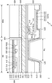
도 1은 본 발명의 일 실시예에 따른 플렉서블 디스플레이 장치를 개략적으로 도시하는 사시도이다.
도 2는 도 1에 도시된 플렉서블 디스플레이 장치의 Ⅱ-Ⅱ 선을 따라 취한 단면을 개략적으로 도시하는 단면도이다.
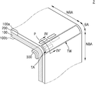
도 3은 본 발명의 일 실시예에 따른 플렉서블 디스플레이 장치를 개략적으로 도시하는 사시도이다.
도 4는 도 3에 도시된 플렉서블 디스플레이 장치의 Ⅳ-Ⅳ 선을 따라 취한 단면을 개략적으로 도시하는 단면도이다.1 is a perspective view schematically showing a flexible display device according to an embodiment of the present invention.
2 is a cross-sectional view schematically showing a cross-section taken along a line II-II of the flexible display device shown in FIG.
3 is a perspective view schematically showing a flexible display device according to an embodiment of the present invention.
4 is a cross-sectional view schematically showing a cross section taken along the line IV-IV of the flexible display device shown in FIG.
본 발명은 다양한 변환을 가할 수 있고 여러 가지 실시예를 가질 수 있는 바, 특정 실시예들을 도면에 예시하고 상세한 설명에 상세하게 설명하고자 한다. 본 발명의 효과 및 특징, 그리고 그것들을 달성하는 방법은 도면과 함께 상세하게 후술되어 있는 실시예들을 참조하면 명확해질 것이다. 그러나 본 발명은 이하에서 개시되는 실시예들에 한정되는 것이 아니라 다양한 형태로 구현될 수 있다. BRIEF DESCRIPTION OF THE DRAWINGS The present invention is capable of various modifications and various embodiments, and specific embodiments are illustrated in the drawings and described in detail in the detailed description. The effects and features of the present invention and methods of achieving them will be apparent with reference to the embodiments described in detail below with reference to the drawings. However, the present invention is not limited to the embodiments described below, but may be implemented in various forms.
이하, 첨부된 도면을 참조하여 본 발명의 실시예들을 상세히 설명하기로 하며, 도면을 참조하여 설명할 때 동일하거나 대응하는 구성 요소는 동일한 도면부호를 부여하고 이에 대한 중복되는 설명은 생략하기로 한다.Hereinafter, exemplary embodiments of the present invention will be described in detail with reference to the accompanying drawings, wherein like reference numerals refer to like or corresponding components throughout the drawings, and a duplicate description thereof will be omitted .
이하의 실시예에서, 제1, 제2 등의 용어는 한정적인 의미가 아니라 하나의 구성 요소를 다른 구성 요소와 구별하는 목적으로 사용되었다. 또한, 단수의 표현은 문맥상 명백하게 다르게 뜻하지 않는 한, 복수의 표현을 포함한다.In the following embodiments, the terms first, second, and the like are used for the purpose of distinguishing one element from another element, not the limitative meaning. Also, the singular expressions include plural expressions unless the context clearly dictates otherwise.
한편, 포함하다 또는 가지다 등의 용어는 명세서상에 기재된 특징, 또는 구성요소가 존재함을 의미하는 것이고, 하나 이상의 다른 특징들 또는 구성요소가 부가될 가능성을 미리 배제하는 것은 아니다. 또한, 막, 영역, 구성 요소 등의 부분이 다른 부분 "위에" 또는 "상에" 있다고 할 때, 다른 부분의 "바로 위에" 또는 "바로 상에" 있는 경우뿐만 아니라, 그 중간에 다른 막, 영역, 구성 요소 등이 개재되어 있는 경우도 포함한다.On the other hand, the terms including or including mean that a feature or element described in the specification is present, and does not preclude the possibility of one or more other features or components being added. It is also to be understood that when a section of a film, an area, an element, etc. is referred to as being "on" or "on" another part, Areas, elements, and the like are interposed.
도면에서는 설명의 편의를 위하여 구성 요소들이 그 크기가 과장 또는 축소될 수 있다. 예컨대, 도면에서 나타난 각 구성의 크기 및 두께는 설명의 편의를 위해 임의로 나타내었으므로, 본 발명이 반드시 도시된 바에 한정되지 않는다.In the drawings, components may be exaggerated or reduced in size for convenience of explanation. For example, the size and thickness of each component shown in the drawings are arbitrarily shown for convenience of explanation, and thus the present invention is not necessarily limited to those shown in the drawings.
x축, y축 및 z축은 직교 좌표계 상의 세 축으로 한정되지 않고, 이를 포함하는 넓은 의미로 해석될 수 있다. 예를 들어, x축, y축 및 z축은 서로 직교할 수도 있지만, 서로 직교하지 않는 서로 다른 방향을 지칭할 수도 있다.The x-axis, y-axis, and z-axis are not limited to three axes on the orthogonal coordinate system, and can be interpreted in a broad sense including this. For example, the x-axis, y-axis, and z-axis may be orthogonal to each other, but may refer to different directions that are not orthogonal to each other.
도 1은 본 발명의 일 실시예에 따른 플렉서블 디스플레이 장치(1)를 개략적으로 도시하는 사시도이다.1 is a perspective view schematically showing a
도 1을 참조하면, 본 발명의 일 실시예에 따른 플렉서블 디스플레이 장치(1)는 일면(100a)과 타면(100b)을 갖는 플렉서블 기판(100), 플렉서블 기판(100)의 일면(100a) 상에 배치되며 투광부(TA)를 갖는 제1 디스플레이부(200) 및 플렉서블 기판(100)의 타면(100b) 상에 배치되는 제2 디스플레이부(300)를 구비한다.1, a
플렉서블 기판(100)은 플렉서블 특성을 갖는 것으로서, 판상 형태로 형성될 수 있으며, 일면(100a) 및 일면(100a)과 반대되는 타면(100b)을 가질 수 있다. 이러한 플렉서블 기판(100)은 예컨대, 금속재, 또는 PET(Polyethylen terephthalate), PEN(Polyethylen naphthalate), 폴리이미드(Polyimide) 등과 같은 플라스틱재 등, 다양한 재료로 형성된 것일 수 있다. The
플렉서블 기판(100)은 벤딩 영역(BA)과 비벤딩 영역(NBA)을 가질 수 있다. 도 1에서는 벤딩 영역(BA)을 기준으로 양측에 비벤딩 영역(NBA)이 형성된 실시예를 도시하고 있으나, 벤딩 영역(BA)은 패널의 엣지(edge)에 위치할 수도 있다. 또한 도 1에서는 벤딩 영역(BA)을 기준으로 양측에 배치된 비벤딩 영역(NBA)이 대략 직각으로 벤딩되어 있는 것으로 도시되어 있으나, 본 발명이 반드시 이에 한정되는 것은 아니며, 벤딩 영역(BA)을 기준으로 양측에 배치된 비벤딩 영역(NBA) 사이의 각도는 다양한 값을 가질 수 있다. 일 실시예에 따르면, 플렉서블 기판(100)은 완전히 접힌 형태일 수도 있다.The
제1 디스플레이부(200)는 플렉서블 기판(100)의 일면(100a) 상에 배치될 수 있다. 도 1에 도시된 것과 같이, 제1 디스플레이부(200)는 플렉서블 기판(100)의 일면(100a)에 전면(全面)에 걸쳐 배치될 수 있다. 제1 디스플레이부(200)는 박막트랜지스터(TFT)들을 포함하며, 이러한 박막트랜지스터(TFT)들과 이에 연결된 화소전극을 포함하는 유기발광 디스플레이부일 수도 있고, 액정 디스플레이부일 수도 있다. 본 실시예에서는 제1 디스플레이부(200)가 유기발광 디스플레이부인 경우에 대하여 설명한다. 이러한 제1 디스플레이부(200)는 복수개의 화소(P)들을 가질 수 있는데, 이러한 화소(P)들은 유기발광소자(OLED)를 포함할 수 있다.The
도시되어 있지는 않으나 제1 디스플레이부(200)의 상부에는 터치스크린패널(TSP) 및/또는 커버윈도우 등이 더 구비될 수 있다.Although not shown, a touch screen panel (TSP) and / or a cover window may be further provided on the
제1 디스플레이부(200)는 외광이 투과할 수 있는 영역으로서 투광부(TA)를 가질 수 있다. 투광부(TA)는 플렉서블 기판(100)의 벤딩 영역(BA)에 대응하여 위치할 수 있다. 이러한 투광부(TA)에는 개구부(OP1)로 형성된 투광창(TW)이 배치될 수 있다.The
구체적으로 투광부(TA)에는 절연층이 위치할 수 있으며, 이러한 절연층이란 후술할 버퍼층(211), 게이트절연막(213) 층간절연막(215), 평탄화막(217) 및 화소정의막(219)의 전부 또는 일부를 통칭하는 것으로 이해될 수 있다. 이 경우 절연층은 제1 개구부(OP1)를 가질 수 있으며, 이는 절연층을 형성하는 상기 복수개의 층들 중 적어도 한 층 이상이 제1 개구부(OP1)를 갖는 것일 수 있다. 이러한 제1 개구부(OP1)는 투광창(TW)에 대응될 수 있다. 따라서 투광부(TA)에는 복수개의 투광창(TW)들이 위치할 수도 있고, 투광창(TW)의 크기에 따라 하나의 투광창(TW)이 투광부(TA) 전체에 대응하도록 할 수도 있다. 구체적으로 제1 디스플레이부(200)는 절연층으로서의 평탄화막(217) 및 화소정의막(219)을 가질 수 있으며, 이러한 평탄화막(217) 및 화소정의막(219)에 투광창(TW)이 형성될 수 있다. 도 2에서는 평탄화막(217) 및 화소정의막(219)에 투광창(TW)이 구비된 것으로 도시되어 있으나, 다른 실시예로 버퍼층(211), 게이트절연막(213) 층간절연막(215), 평탄화막(217) 또는 화소정의막(219) 중 하나 또는 선택적 층에만 투광창(TW)이 구비될 수도 있다.Specifically, the insulating layer may be located in the transparent portion TA. The insulating layer includes a
이러한 투광창(TW)은 복수개 구비될 수 있는데, 이 경우 비벤딩 영역(NBA)에 위치한 화소(P)들과 대략 동일한 크기로 형성될 수도 있다. 즉, 도 1에 도시된 것과 같이 화소정의막(219)이 화소(P)들 각각의 화소영역을 정의하도록 제2 개구부(OP2)를 가지며, 이러한 화소(P)들 각각의 제2 개구부(OP2)와 투광부(TA)의 제1 개구부(OP1)인 투광창(TW)들 각각이 동일한 크기로 형성될 수 있다.In this case, the light transmitting window TW may be formed to have substantially the same size as the pixels P located in the non-bending region NBA. That is, as shown in FIG. 1, the
다른 실시예로 도 3 및 도 4에 도시된 것과 같이, 투광부(TA)에 위치한 투광창(TW)은 비벤딩 영역(NBA)에 위치한 화소(P)들 각각 보다 큰 크기로 형성될 수도 있으며, 투광부(TA) 전체에 대응되는 크기로 형성될 수도 있다. In another embodiment, as shown in FIGS. 3 and 4, the light-transmitting window TW located in the light-transmitting portion TA may be formed to have a larger size than each of the pixels P located in the non-bending region NBA , And the entire size of the transparent portion (TA).
이러한 투광부(TA)에는 유기발광소자(OLED)가 위치하지 않을 수 있다. 즉 투광부(TA)에 위치한 투광창(TW) 내에는 유기발광소자(OLED)가 위치하지 않을 수 있으며, 이러한 투광창(TW)은 후술할 제2 디스플레이부(300)에서 발광하는 빛을 플렉서블 기판(100)을 지나 제1 디스플레이부(200) 측으로 투과시키는 창문의 역할을 할 수 있다. 이때 투명창이란 빛을 투과할 수 있을 정도의 투명도를 의미하는 것으로 이해될 수 있다.The organic light emitting diode OLED may not be disposed in the transparent portion TA. That is, the organic light emitting diode OLED may not be located in the light transmitting window TW located in the light transmitting portion TA. The light transmitting window TW may be a flexible light emitting window, And may serve as a window for passing through the
제2 디스플레이부(300)는 플렉서블 기판(100)의 타면(100b) 상에 배치될 수 있다. 제2 디스플레이부(300)는 박막트랜지스터(TFT)와 이에 연결된 발광소자를 포함하는 디스플레이부일 수 있으며, 본 실시예에서는 제2 디스플레이부(300)는 발광소자로서 발광 다이오드(LED)를 포함할 수 있다. 본 실시예의 발광 다이오드(LED)는 마이크로 LED일 수 있다. 여기서 마이크로는 1 내지 100 ㎛ 의 크기를 가리킬 수 있으나, 본 발명의 실시예들은 이에 제한되지 않고, 그보다 더 크거나 더 작은 크기의 발광 다이오드에도 적용될 수 있다.The
플렉서블 기판(100)을 기준으로 일면(100a)에는 제1 디스플레이부(200)가 배치되고, 타면(100b)에는 제2 디스플레이부(300)가 배치될 수 있다. 도 1에 도시된 것과 같이 플렉서블 기판(100)은 벤딩 영역(BA)과 비벤딩 영역(NBA)을 포함할 수 있는데, 제2 디스플레이부(300)는 플렉서블 기판(100)의 벤딩 영역(BA)에 대응하여 배치될 수 있다. 즉 제2 디스플레이부(300)는 플렉서블 기판(100)의 타면(100b) 상의 일부에만 배치될 수 있다. 이는 제2 디스플레이부(300)가 제1 디스플레이부(200)의 투광부(TA)에 대응하도록 배치되는 것을 의미한다. 이를 통해 제2 디스플레이부(300)에서 방출된 빛은 플렉서블 기판(100)을 통과해 제1 디스플레이부(200)의 투광부(TA)를 통해 외부로 방출될 수 있다.The
도 2는 도 1에 도시된 플렉서블 디스플레이 장치(1)의 Ⅱ-Ⅱ 선을 따라 취한 단면을 개략적으로 도시하는 단면도이다.2 is a cross-sectional view schematically showing a cross section taken along a line II-II of the
도 1 및 도 2를 함께 참조하면, 본 발명의 일 실시예에 따른 플렉서블 디스플레이 장치(1)는 플렉서블 기판(100)의 일면(100a) 상에 배치된 제1 디스플레이부(200) 및 플렉서블 기판(100)의 타면(100b) 상에 배치된 제2 디스플레이부(300)를 포함한다.1 and 2, a
상술한 것과 같이 제1 디스플레이부(200)는 플렉서블 기판(100)의 일면(100a)의 전면(全面)에 걸쳐 배치될 수 있다. 즉 플렉서블 기판(100)은 벤딩 영역(BA)과 비벤딩 영역(NBA)을 가질 수 있으며, 제1 디스플레이부(200)는 플렉서블 기판(100)의 벤딩 영역(BA)과 비벤딩 영역(NBA)에 걸쳐 배치될 수 있다. 비벤딩 영역(NBA) 상에 배치된 제1 디스플레이부(200)는 각각이 유기발광소자(OLED)를 포함하는 화소(P)들을 구비할 수 있다.The
먼저 플렉서블 기판(100) 상에는 플렉서블 기판(100)의 면을 평탄화하기 위해 또는 박막트랜지스터(TFT)의 반도체층(212)으로 불순물 등이 침투하는 것을 방지하기 위해, 실리콘옥사이드 또는 실리콘나이트라이드 등으로 형성된 버퍼층(211)이 배치되고, 이 버퍼층(211) 상에 반도체층(212)이 위치하도록 할 수 있다.First, in order to planarize the surface of the
반도체층(212)의 상부에는 게이트전극(214)이 배치되는데, 이 게이트전극(214)에 인가되는 신호에 따라 소스전극(216a) 및 드레인전극(216b)이 전기적으로 소통된다. 게이트전극(214)은 인접층과의 밀착성, 적층되는 층의 표면 평탄성 그리고 가공성 등을 고려하여, 예컨대 알루미늄(Al), 백금(Pt), 팔라듐(Pd), 은(Ag), 마그네슘(Mg), 금(Au), 니켈(Ni), 네오디뮴(Nd), 이리듐(Ir), 크롬(Cr), 리튬(Li), 칼슘(Ca), 몰리브덴(Mo), 티타늄(Ti), 텅스텐(W), 구리(Cu) 중 하나 이상의 물질로 단층 또는 다층으로 형성될 수 있다.A
이때 반도체층(212)과 게이트전극(214)과의 절연성을 확보하기 위하여, 실리콘옥사이드 및/또는 실리콘나이트라이드 등으로 형성되는 게이트절연막(213)이 반도체층(212)과 게이트전극(214) 사이에 개재될 수 있다.A
게이트전극(214)의 상부에는 층간절연막(215)이 배치될 수 있는데, 이는 실리콘옥사이드 또는 실리콘나이트라이드 등의 물질로 단층으로 형성되거나 또는 다층으로 형성될 수 있다.An interlayer insulating
층간절연막(215)의 상부에는 소스전극(216a) 및 드레인전극(216b)이 배치된다. 소스전극(216a) 및 드레인전극(216b)은 층간절연막(215)과 게이트절연막(213)에 형성되는 컨택홀을 통하여 반도체층(212)에 각각 전기적으로 연결된다. 소스전극(216a) 및 드레인전극(216b)은 도전성 등을 고려하여 예컨대 알루미늄(Al), 백금(Pt), 팔라듐(Pd), 은(Ag), 마그네슘(Mg), 금(Au), 니켈(Ni), 네오디뮴(Nd), 이리듐(Ir), 크롬(Cr), 리튬(Li), 칼슘(Ca), 몰리브덴(Mo), 티타늄(Ti), 텅스텐(W), 구리(Cu) 중 하나 이상의 물질로 단층 또는 다층으로 형성될 수 있다.A
한편 도면에는 도시되지 않았으나, 이러한 구조의 박막트랜지스터(TFT)의 보호를 위해 박막트랜지스터(TFT)를 덮는 보호막(미도시)이 배치될 수 있다. 보호막은 예컨대 실리콘옥사이드, 실리콘나이트라이드 또는 실리콘옥시나이트라이드 등과 같은 무기물로 형성될 수 있다.Although not shown in the drawing, a protective film (not shown) for covering the thin film transistor (TFT) may be disposed for protecting the thin film transistor (TFT) having such a structure. The protective film may be formed of an inorganic material such as silicon oxide, silicon nitride or silicon oxynitride.
한편, 플렉서블 기판(100)의 상에 평탄화막(217)이 배치될 수 있다. 이 경우 평탄화막(217)은 평탄화막일 수도 있고 보호막일 수도 있다. 이러한 평탄화막(217)은 박막트랜지스터(TFT) 상부에 유기발광소자가 배치되는 경우 박막트랜지스터(TFT) 의 상면을 대체로 평탄화하게 하고, 박막트랜지스터(TFT) 및 각종 소자들을 보호하는 역할을 한다. 이러한 평탄화막(217) 은 예컨대 아크릴계 유기물 또는 BCB(Benzocyclobutene) 등으로 형성될 수 있다. 이때 버퍼층(211), 게이트절연막(213), 층간절연막(215) 및 평탄화막(217)은 플렉서블 기판(100)의 전면(全面)에 형성될 수 있다. 다만 이 경우에도 도 2에 도시된 것과 같이 투광창(TW)에는 평탄화막(217)이 배치되지 않을 수 있다. 다른 실시예로, 투광창(TW)의 빛 투과도를 높이기 위해 투광창(TW)에 버퍼층(211), 게이트절연막(213) 층간절연막(215) 중 일부가 배치되지 않을 수 있다.On the other hand, the
한편, 박막트랜지스터(TFT) 상부에는 화소정의막(219)이 배치될 수 있다. 화소정의막(219)은 플렉서블 기판(100)의 전면에 걸쳐 배치될 수 있으며, 상술한 평탄화막(217) 상에 위치할 수 있다. 화소정의막(219)은 벤딩 영역(BA) 상에 위치한 제1 개구부(OP1)로써 투광창(TW) 영역을 정의하며, 투광창(TW)을 비벤딩 영역(NBA) 상에 위치한 제2 개구부(OP2)로써 화소영역을 정의할 수 있다.On the other hand, a
이러한 화소정의막(219)은 예컨대 유기 절연막으로 구비될 수 있다. 그러한 유기 절연막으로는 폴리메틸메타크릴레이트(PMMA)와 같은 아크릴계 고분자, 폴리스티렌(PS), phenol그룹을 갖는 고분자 유도체, 이미드계 고분자, 아릴에테르계 고분자, 아마이드계 고분자, 불소계고분자, p-자일렌계 고분자, 비닐알콜계 고분자 및 이들의 혼합물 등을 포함할 수 있다.The
한편, 비벤딩 영역(NBA) 상에는 유기발광소자(OLED)가 배치될 수 있다. 유기발광소자(OLED)는 평탄화막(217) 상에 배치될 수 있으며, 화소전극(220), 발광층(EML: Emission Layer)을 포함하는 중간층(230) 및 대향전극(240)을 포함할 수 있다.On the other hand, the organic light emitting device OLED may be disposed on the non-bending region NBA. The organic light emitting diode OLED may be disposed on the
화소전극(220)은 (반)투명 전극 또는 반사형 전극으로 형성될 수 있다. (반)투명 전극으로 형성될 때에는 예컨대 ITO, IZO, ZnO, In2O3, IGO 또는 AZO로 형성될 수 있다. 반사형 전극으로 형성될 때에는 Ag, Mg, Al, Pt, Pd, Au, Ni, Nd, Ir, Cr 및 이들의 화합물 등으로 형성된 반사막과, ITO, IZO, ZnO, In2O3, IGO 또는 AZO로 형성된 층을 가질 수 있다. 물론 본 발명이 이에 한정되는 것은 아니고 다양한 재질로 형성될 수 있으며, 그 구조 또한 단층 또는 다층이 될 수 있는 등 다양한 변형이 가능하다.The
화소정의막(219)에 의해 정의된 화소영역에는 중간층(230)이 배치될 수 있다. 이러한 중간층(230)은 전기적 신호에 의해 빛을 발광하는 발광층(EML: Emission Layer)을 포함하며, 발광층(EML) 이외에도 발광층(EML)과 화소전극(220) 사이에 배치되는 홀 주입층(HIL: Hole Injection Layer), 홀 수송층(HTL: Hole Transport Layer) 및 발광층(EML)과 대향전극(240) 사이에 배치되는 전자 수송층(ETL: Electron Transport Layer), 전자 주입층(EIL: Electron Injection Layer) 등이 단일 혹은 복합의 구조로 적층되어 형성될 수 있다. 물론 중간층(230)은 반드시 이에 한정되는 것은 아니고, 다양한 구조를 가질 수도 있음은 물론이다.The
발광층(EML)을 포함하는 중간층(230)을 덮으며 화소전극(220)에 대향하는 대향전극(240)이 플렉서블 기판(100) 전면(全面)에 걸쳐서 배치될 수 있다. 대향전극(240)은 (반)투명 전극 또는 반사형 전극으로 형성될 수 있다.The
대향전극(240)이 (반)투명 전극으로 형성될 때에는 일함수가 작은 금속 즉, Li, Ca, LiF/Ca, LiF/Al, Al, Ag, Mg 및 이들의 화합물로 형성된 층과 ITO, IZO, ZnO 또는 In2O3 등의 (반)투명 도전층을 가질 수 있다. 대향전극(240)이 반사형 전극으로 형성될 때에는 Li, Ca, LiF/Ca, LiF/Al, Al, Ag, Mg 및 이들의 화합물로 형성된 층을 가질 수 있다. 물론 대향전극(240)의 구성 및 재료가 이에 한정되는 것은 아니며 다양한 변형이 가능함은 물론이다.When the
대향전극(240) 상에는 박막봉지층(250)이 위치할 수 있다. 박막봉지층(250)은 제1 디스플레이부(200) 전면에 걸쳐 배치될 수 있으며, 단층 또는 다층구조로 형성될 수 있다. 박막봉지층(250)이 다층구조로 형성되는 경우에는 유기막 및 무기막 또는 유무기 복합막이 교번하여 적층된 형태로 구비될 수 있다. 이러한 박막봉지층(250)은 외부 투습으로부터 제1 디스플레이부(200)를 보호하는 기능을 할 수 있다. The thin
한편, 플렉서블 기판(100)의 벤딩 영역(BA) 상에는 제1 디스플레이부(200)의 투광부(TA)가 위치할 수 있다. 전술한 것과 같이 투광부(TA)에는 유기발광소자(OLED)가 배치되지 않는다. 대신 투광부(TA)는 적어도 하나의 투광창(TW)을 포함할 수 있으며, 이 투광창(TW)을 통해 제2 디스플레이부(300)에서 발광한 빛이 플렉서블 기판(100)을 통과하여 투과될 수 있다. On the other hand, the transparent portion TA of the
도 2에 도시된 것과 같이 투광창(TW)에는 플렉서블 기판(100) 전면에 배치된 버퍼층(211), 게이트절연막(213) 및 층간절연막(215)이 배치될 수 있으며, 대향전극(240) 및 박막봉지층(250)이 배치될 수 있다. 다른 실시예로 대향전극(240) 또는 박막봉지층(250)이 배치될 수도 있으며, 대향전극(240)과 박막봉지층(250)이 배치되지 않고 투광창(TW)을 통해 버퍼층(211), 게이트절연막(213) 또는 층간절연막(215) 중 일부가 노출될 수도 있다. 다른 실시예로 투광부(TA)의 투광창(TW)에는 어떠한 층들도 배치되지 않을 수 있고, 투광창(TW)을 통해 플렉서블 기판(100)이 노출될 수도 있다.2, a
본 실시예에서 벤딩 영역(BA) 상에 위치한 투광부(TA)의 투광창(TW)은 비벤딩 영역(NBA) 상에 위치한 화소(P)들과 동일 또는 유사한 크기를 갖도록 패터닝될 수 있다. 도 2에서는 하나의 투광창(TW)만을 도시하였으나, 벤딩 영역(BA) 상에 위치한 투광부(TA)는 복수개의 투광창(TW)들을 포함할 수 있음은 물론이다.The light transmitting window TW of the light transmitting portion TA located on the bending area BA in this embodiment may be patterned to have the same or similar size as the pixels P located on the non-bending area NBA. Although only one light transmitting window TW is shown in FIG. 2, it is needless to say that the light transmitting portion TA located on the bending area BA may include a plurality of light transmitting windows TW.
도 2에 도시된 것과 같이 투광부(TA)의 투광창(TW) 내에도 일부 절연막이 배치될 수 있는데, 투광부(TA)의 투광창(TW)을 통해 제2 디스플레이부(300)에서 발광한 빛이 투과되어야 하기 위해서는, 투광부(TA)의 투광창(TW) 내에 위치하는 버퍼층(211), 게이트절연막(213) 및 층간절연막(215)는 투명 또는 반투명한 물질로 형성되는 것이 바람직하다. 이는 박막봉지층(250)의 경우에도 마찬가지이며, 도 2에 도시된 것과 같이 대향전극(240)이 플렉서블 기판(100) 전면에 형성되어, 투광부(TA)의 투광창(TW) 내에도 위치하는 경우 대향전극(240)은 투명 또는 반투명 전극으로 형성되는 것이 바람직하다.A part of the insulating film may be disposed in the light transmitting window TW of the transparent portion TA as shown in FIG. 2. The light emitted from the
한편, 플렉서블 기판(100)의 타면(100b) 상에는 제2 디스플레이부(300)가 위치할 수 있다. 이러한 제2 디스플레이부(300)는 플렉서블 기판(100)의 타면(100b)의 벤딩 영역(BA) 상에 배치될 수 있다. 즉 제2 디스플레이부(300)는 플렉서블 기판(100)의 일면(100a)에 배치되는 제1 디스플레이부(200)의 투광부(TA)에 대응하도록 배치되는 것으로 이해될 수 있다. 즉 제1 디스플레이부(200)의 투광부(TA)에는 유기발광소자(OLED)가 배치되지 않는 대신, 투광부(TA)에 대응하도록 플렉서블 기판(100)의 타면(100b)에 배치된 제2 디스플레이부(300)에서 발광된 빛이 플렉서블 기판(100)을 통해 제1 디스플레이부(200) 측으로 발광될 수 있도록 한다.On the other hand, the
제2 디스플레이부(300)는 플렉서블 기판(310), 플렉서블 기판(310) 상에 배치된 박막트랜지스터(TFT)와 이에 전기적으로 연결된 발광 다이오드(LED)를 구비한다. 도 2에서는 플렉서블 기판(310) 상에 박막트랜지스터(TFT)의 반도체층(312)이 바로 배치된 것으로 도시되어 있으나, 경우에 따라 버퍼층(미도시)이 사이에 개재될 수 있다. 반도체층(312)의 상부에는 반도체층(312)의 적어도 일부와 중첩되도록 게이트전극(314)이 위치할 수 있으며, 반도체층(312)과 게이트전극(314)의 절연을 위해 게이트절연막(315)이 개재될 수 있다. 게이트전극(314) 상에 배치되는 층간절연막(315)의 상부에는 소스전극(316)(또는 드레인전극) 및 드레인전극(318)(또는 소스전극)이 배치된다. 소스전극(316) 및 드레인전극(318)은 층간절연막(315)과 게이트절연막(313)에 형성되는 컨택홀을 통하여 반도체층(312)에 각각 전기적으로 연결된다.The
이와 같이 제2 디스플레이부(300)에 포함된 박막트랜지스터(TFT)는 제1 디스플레이부(200)에 포함된 박막트랜지스터(TFT)와 실질적으로 동일한 바 중복되는 설명은 생략한다.The thin film transistor (TFT) included in the
또한 본 실시예에서 제1 디스플레이부(200)의 박막트랜지스터(TFT)와 제2 디스플레이부(300)의 박막트랜지스터(TFT)는 게이트 전극이 활성층의 상부에 배치된 탑 게이트 타입(top gate type)을 예시하였지만, 본 발명은 이에 제한되지 않으며, 게이트 전극은 활성층의 하부에 배치될 수도 있다.In this embodiment, the thin film transistor (TFT) of the
박막트랜지스터(TFT) 상에는 제1 절연막(330)이 배치될 수 있는데, 제1 절연막(330)은 박막트랜지스터(TFT) 상부를 보호하며 상면을 평탄하게 할 수 있다. 이러한 제1 절연막(330)은 오목부(330a)를 가질 수 있으며, 오목부(330a)를 통해 층간절연막(315) 상에 배치된 제1 전극(318) 및 제2 전극(320)이 외부로 노출될 수 있다. 오목부(330a) 내에는 발광 다이오드(LED, 350)가 실장될 수 있으며, 발광 다이오드(350)는 오목부(330a)를 통해 노출된 제1 전극(318) 및 제2 전극(320)과 전기적으로 연결될 수 있다. 본 실시예에서 제1 전극(318)은 박막트랜지스터(TFT)의 드레인전극(318)(또는 소스전극)이 연장되어 형성될 수 있다. 다른 실시예로 제1 전극(318)은 별도의 층으로 구비될 수도 있다.A first insulating
제1 전극(318)은 반사 전극으로 구성될 수 있고, 하나 또는 하나 이상의 층을 포함할 수 있다. 예를 들어, 제1 전극(318)은 알루미늄, 몰리브덴, 티타늄, 티타늄과 텅스턴, 은, 또는 금, 또는 그것의 합금과 같은 금속을 포함할 수 있다. 제1 전극(318)은 ITO, IZO, ZnO, 또는 In2O3 등의 투명 도전성 산화물(TCO), 카본 나노 튜브 필름 또는 투명한 도전성 폴리머와 같은 도전성 물질을 포함하는 투명 도전층, 및 반사층을 포함할 수 있다. 일 실시예에서, 제1 전극(318)은 상부 및 하부 투명 도전층과 그 사이의 반사층을 포함하는 3중층일 수 있다. 제2 전극(320)은 투명 또는 반투명 전극으로 구성될 수 있다. 예를 들어, 제2 전극(320)은 전술된 투명 도전성 물질로 형성될 수 있고, Ag, Al, Mg, Li, Ca, Cu, LiF/Ca, LiF/Al, MgAg 및 CaAg에서 선택된 하나 이상의 물질을 포함할 수 있다.The
발광 다이오드(350)는 마이크로 LED일 수 있다. 여기서 마이크로는 1 내지 100 ㎛ 의 크기를 가리킬 수 있으나, 본 발명의 실시예들은 이에 제한되지 않고, 그보다 더 크거나 더 작은 크기의 발광 다이오드에도 적용될 수 있다. 발광 다이오드(350)는 개별적으로 또는 복수 개가 이송 기구에 의해 웨이퍼 상에서 픽업(pick up)되어 플렉서블 기판(310)에 전사됨으로써 오목부(330a)에 수용될 수 있다. 발광 다이오드(350)는 적색, 녹색, 청색, 백색 LED 또는 UV LED일 수 있다.The
발광 다이오드(350)는 p-n 다이오드(미도시), 제1 컨택 전극(미도시) 및 제2 컨택 전극(미도시)을 포함할 수 있다. 제1 컨택 전극 및/또는 제2 컨택 전극은 하나 이상의 층을 포함할 수 있으며, 금속, 전도성 산화물 및 전도성 중합체들을 포함한 다양한 전도성 재료로 형성될 수 있다. 제1 컨택 전극 및 제2 컨택 전극은 반사층, 예를 들어, 은(silver) 층을 선택적으로 포함할 수 있다. 제1 컨택 전극은 제1 전극(318)과 전기적으로 연결되고, 제2 컨택 전극은 제2 전극(320)과 전기적으로 연결된다. 일 실시예로, p-n 다이오드는 p-도핑층, 하나 이상의 양자 우물 층 및 n-도핑층을 포함할 수 있다.The
도 2에서는 수평형 마이크로 LED를 예로서 도시하였으나, 본 발명의 실시예는 이에 한정되지 않고, 제1 컨택 전극과 제2 컨택 전극이 같은 방향을 향해 배치되는 플립형 마이크로 LED, 수직형 마이크로 LED 등일 수 있다. 이 경우, 제1 전극 및 제2 전극의 위치는 발광 다이오드(350)의 제1 컨택 전극(미도시) 및 제2 컨택 전극(미도시)의 위치에 대응하게 배치될 수 있다.2, the embodiments of the present invention are not limited thereto, and the first contact electrode and the second contact electrode may be flip-type micro LEDs arranged in the same direction, a vertical micro LED, or the like. have. In this case, the positions of the first electrode and the second electrode may be arranged corresponding to the positions of the first contact electrode (not shown) and the second contact electrode (not shown) of the
한편, 도시되어 있지는 않으나, 발광 다이오드(350)가 플렉서블 기판(100) 측으로 빛을 발광하게 하기 위하여 플렉서블 기판(310)과 발광 다이오드(350) 사이에 반사막 등을 더 구비할 수 있다.Although not shown, a reflective film may be additionally provided between the
발광 다이오드(350)의 상부에는 발광 다이오드(350)를 보호하며 상면을 평탄하게 하기 위한 제2 절연막(340)이 배치될 수 있다. 제2 절연막(340)과 전술한 제1 절연막(330)은 유기 절연막으로 구비될 수 있다. 그러한 유기 절연막으로는 폴리메틸메타크릴레이트(PMMA)와 같은 아크릴계 고분자, 폴리스티렌(PS), phenol그룹을 갖는 고분자 유도체, 이미드계 고분자, 아릴에테르계 고분자, 아마이드계 고분자, 불소계고분자, p-자일렌계 고분자, 비닐알콜계 고분자 및 이들의 혼합물 등을 포함할 수 있다.A second insulating
제2 디스플레이부(300)와 플렉서블 기판(100)의 타면(100b) 사이에는 접착층(510)이 개재될 수 있다. 즉 제2 디스플레이부(300)는 접착층(510)을 통해 플렉서블 기판(100)의 타면(100b)에 부착될 수 있다. 이 경우 접착층(510)은 빛이 발광하는 방향에 배치되기 때문에 투명 접착 물질로 형성되는 것이 바람직하며, 예컨대 OCA(Optically Clear Adhesive) 또는 OCR(Optically Clear Resin) 등으로 형성될 수 있다.An
한편, 플렉서블 기판(100)의 타면(100b) 상에는 보호필름(400)이 배치될 수 있는데, 도 2에 도시된 것과 같이 보호필름(400)은 제2 디스플레이부(300)가 배치되지 않은 부분에 위치할 수 있다. 즉, 플렉서블 기판(100)의 벤딩 영역(BA)에 대응하여 제2 디스플레이부(300)가 배치되는 경우, 보호필름(400)은 플렉서블 기판(100)의 비벤딩 영역(NBA)에 대응하여 배치될 수 있다. 보호필름(400)과 플렉서블 기판(100) 사이에는 접착층(520)이 배치될 수 있으며, 접착층(520)은 상술한 접착층(510)과 동일한 물질로 형성될 수도 있고, 다른 물질로 형성될 수도 있다. 보호필름(400)은 플렉서블한 플라스틱재로 형성될 수 있으며, 예컨대 PET와 같은 물질로 형성될 수 있다. 보호필름(400)과 제2 디스플레이부(300)는 서로 소정 간격 이격되어 배치될 수 있으며 사이에 홈(530)이 형성될 수도 있다. 다른 실시예로 보호필름(400)과 제2 디스플레이부(300)는 이격된 공간 없이 서로 접하여 배치될 수도 있다.2, the
한편 도 1 및 도 2를 함께 참조하면, 제1 디스플레이부(200)는 복수개의 유기발광소자(OLED)들을 포함할 수 있고, 제2 디스플레이부(300)는 복수개의 발광 다이오드(LED)들을 포함할 수 있다. 복수개의 유기발광소자(OLED)들은 일 방향(X축 방향 또는 Y축 방향)을 따라 제1 간격으로 이격되어 배치될 수 있으며, 복수개의 발광 다이오드(LED)들은 일 방향(X축 방향 또는 Y축 방향)을 따라 제2 간격으로 이격되어 배치될 수 있다. 본 실시예에서는 제1 간격과 제2 간격은 동일할 수도 있다. 다른 실시예로 제1 간격과 제2 간격은 서로 상이할 수 있다.1 and 2, the
종래의 플렉서블 디스플레이 장치에서는 벤딩 영역(BA) 상에 배치된 유기발광소자(OLED)에 발생되는 잦은 불량으로 인해 디스플레이 장치 전체의 수율이 떨어지고 신뢰성이 저하되는 등의 문제점이 있었다.In the conventional flexible display device, there is a problem that the yield of the entire display device is lowered and reliability is lowered due to frequent defects occurring in the organic light emitting device OLED disposed on the bending area BA.
이에 본 발명의 일 실시예에 따른 플렉서블 디스플레이 장치(1)에서는 플렉서블 기판(100)의 일면(100a) 상에 배치된 제1 디스플레이부(200)에 있어서, 벤딩 영역(BA)과 대응되도록 투광부(TA)를 구비하며, 이 투광부(TA)를 통해 플렉서블 기판(100)의 타면(100b) 상에 배치된 제2 디스플레이부(300)에 의해 발광된 빛이 플렉서블 기판(100)을 통과하여 투과될 수 있다. 본 실시예에서는 제2 디스플레이부(300)에 마이크로 단위의 발광 다이오드(LED, 350)를 구비함으로써 벤딩 영역(BA)을 구비한 플렉서블 디스플레이 장치(2) 전체의 신뢰성을 향상시킬 수 있다. In the
또한, 플렉서블 디스플레이 장치(2)의 제1 디스플레이부(200)에 투광창(TW)을 구비함으로써, 제2 디스플레이부(300)를 통해 벤딩 영역(BA)에 이미지를 자유롭게 디스플레이 할 수 있고, 특히 제1 디스플레이부(200)가 발광하지 않는 경우에도 제2 디스플레이부(300)를 통해 벤딩 영역(BA)에만 별도의 정보 등을 표시할 수 있다.By providing the translucent window TW on the
도 3은 본 발명의 일 실시예에 따른 플렉서블 디스플레이 장치(2)를 개략적으로 도시하는 사시도이고, 도 4는 도 3의 플렉서블 디스플레이 장치(2)를 Ⅳ-Ⅳ 선을 따라 취한 단면을 개략적으로 도시하는 단면도이다.FIG. 3 is a perspective view schematically showing a
도 3을 참조하면, 본 발명의 일 실시예에 따른 플렉서블 디스플레이 장치(2)는 일면(100a)과 타면(100b)을 갖는 플렉서블 기판(100), 플렉서블 기판(100)의 일면(100a) 상에 배치되며 투광부(TA)를 갖는 제1 디스플레이부(200) 및 플렉서블 기판(100)의 타면(100b) 상에 배치되는 제2 디스플레이부(300)를 구비한다. 3, the
도 3의 실시예에 따른 플렉서블 디스플레이 장치(2)의 플렉서블 기판(100)은 벤딩 영역(BA)과 비벤딩 영역(NBA)을 구비하며, 도 1의 플렉서블 디스플레이 장치(1)와 벤딩 영역(BA)에 대응하는 구조에서 차이가 있다. 따라서 이하에서는 벤딩 영역(BA)에 대응하는 구조의 차이점을 중심으로 설명하며, 비벤딩 영역(NBA)에 대응하여 위치하는 제1 디스플레이부(200)의 화소(P)들 및 보호필름(400) 등의 설명은 전술한 도 1의 플렉서블 디스플레이 장치(1)의 설명을 원용한다.The
도 3을 참조하면, 본 발명의 일 실시예에 따른 플렉서블 디스플레이 장치(2)에서는 벤딩 영역(BA)에 대응하여 제1 디스플레이부(200)가 투광부(TA)를 구비할 수 있다. Referring to FIG. 3, in the
투광부(TA)는 투광창(TW)을 가질 수 있는데, 이러한 투광창(TW)은 절연층에 형성된 제1 개구부(OP1)로 이해될 수 있다. 구체적으로 제1 디스플레이부(200)는 절연층으로서의 평탄화막(217) 및 화소정의막(219)을 가질 수 있으며, 이러한 평탄화막(217) 및 화소정의막(219)에 투광창(TW)이 형성될 수 있다. 도 2에서는 평탄화막(217) 및 화소정의막(219)에 투광창(TW)이 구비된 것으로 도시되어 있으나, 다른 실시예로 평탄화막(217) 또는 화소정의막(219) 중 하나에만 투광창(TW)이 구비될 수도 있다.The light transmitting portion TA may have a light transmitting window TW, which can be understood as a first opening OP1 formed in the insulating layer. The
이러한 투광창(TW)은 벤딩 영역(NBA)과 대략 동일한 크기로 형성될 수도 있다. 즉, 도 3 및 도 4에 도시된 것과 같이, 투광부(TA)에 위치한 투광창(TW)은 비벤딩 영역(NBA)에 위치한 화소(P)들 각각 보다 큰 크기로 형성될 수도 있으며, 투광부(TA) 전체에 대응되는 크기로 형성될 수도 있다. The light transmitting window TW may be formed to have substantially the same size as the bending area NBA. 3 and 4, the light transmitting window TW located in the light transmitting portion TA may be formed to have a larger size than each of the pixels P located in the non-bending region NBA, Or may be formed to have a size corresponding to the entire light portion TA.
본 실시예에서는 투광부(TA)는 제1 개구부(OP1)에 대응하는 투광창(TW)을 포함할 수 있으며, 전술한 플렉서블 디스플레이 장치(1)의 투광창(TW)이 화소(P)들의 크기에 맞춰 패터닝되었던 것과는 달리, 본 실시예에서의 투광창(TW)은 벤딩 영역(BA)의 전 영역을 노출하는 형태일 수 있다. 다른 실시예로, 이러한 투광창(TW)은 일측 또는 타측이 개방된 구조일 수도 있다. 다시 말해 제1 디스플레이부(200)에 있어서 투광부(TA)의 투광창(TW)이 배치된 영역은 플렉서블 기판(100)의 벤딩 영역(BA)에 대응할 수 있다. In the present embodiment, the transparent portion TA may include a translucent window TW corresponding to the first opening OP1, and the translucent window TW of the above-described
도 4를 참조하면, 제1 디스플레이부(200)는 투광창(TW)을 포함하는 투광부(TA)를 구비하며, 투광창(TW)은 플렉서블 기판(100)의 벤딩 영역(BA) 전체에 대응할 수 있다. 따라서 플렉서블 기판(100)의 타면(100b)에 배치된 제2 디스플레이부(300)는 복수개의 발광 다이오드(350)들이 투광부(TA)의 투광창(TW)에 대응하도록 배치될 수 있다. 4, the
도 4에서는 플렉서블 기판(310) 상에 복수개의 오목부(330a)들이 형성된 절연막(330)이 배치되며, 이러한 오목부(330a) 내에 발광 다이오드(350)가 각각 실장되는 것으로 이해될 수 있다. 도 4에서는 플렉서블 기판(310) 상에 발광 다이오드(350)들이 직접 배치되는 것으로 도시되어 있으나, 플렉서블 기판(310) 상에 각종 층들이 형성되고 그러한 층들 상에 발광 다이오드(350)가 위치하는 경우를 포함하는 것은 물론이다. 예컨대, 플렉서블 기판(310) 상에 박막트랜지스터가 배치되고, 평탄화막이 이러한 박막트랜지스터를 덮도록 하며, 박막트랜지스터와 전기적으로 연결되는 전극이 그러한 평탄화막 상에 위치하도록 할 수도 있다.4, an insulating
본 실시예에서 발광 다이오드(350)는 마이크로 LED일 수 있다. 여기서 마이크로는 1㎛ 내지 100㎛ 의 크기를 가리킬 수 있으나, 본 발명의 실시예들은 이에 제한되지 않고, 그보다 더 크거나 더 작은 크기의 발광 다이오드에도 적용될 수 있다. 발광 다이오드(350)는 개별적으로 또는 복수 개가 이송 기구에 의해 웨이퍼 상에서 픽업(pick up)되어 플렉서블 기판(310)에 전사됨으로써 오목부(330a)에 수용될 수 있다. 발광 다이오드(350)는 적색, 녹색, 청색, 백색 LED 또는 UV LED일 수 있다.In this embodiment, the
이와 같이 발광 다이오드(350) 및 이를 포함하는 제2 디스플레이 구조에 대하여는 전술한 도 2의 실시예와 중복되는 바 이를 원용한다.As described above, the
종래의 플렉서블 디스플레이 장치에서는 벤딩 영역(BA) 상에 배치된 유기발광소자(OLED)에 발생되는 잦은 불량으로 인해 디스플레이 장치 전체의 수율이 떨어지고 신뢰성이 저하되는 등의 문제점이 있었다.In the conventional flexible display device, there is a problem that the yield of the entire display device is lowered and reliability is lowered due to frequent defects occurring in the organic light emitting device OLED disposed on the bending area BA.
이에 본 발명의 일 실시예에 따른 플렉서블 디스플레이 장치(2)에서는 플렉서블 기판(100)의 일면(100a) 상에 배치된 제1 디스플레이부(200)에 있어서, 벤딩 영역(BA)과 대응되도록 투광부(TA)를 구비하며, 이 투광부(TA)에 형성된 투광창(TW)을 통해 플렉서블 기판(100)의 타면(100b) 상에 배치된 제2 디스플레이부(300)에 의해 발광된 빛이 플렉서블 기판(100)을 통과하여 투과될 수 있다. 본 실시예에서는 제2 디스플레이부(300)에 마이크로 단위의 발광 다이오드(LED, 350)를 구비함으로써 벤딩 영역(BA)을 구비한 플렉서블 디스플레이 장치(2) 전체의 신뢰성을 향상시킬 수 있다. In the
또한, 플렉서블 디스플레이 장치(2)의 제1 디스플레이부(200)에 투광창(TW)을 구비함으로써, 제2 디스플레이부(300)를 통해 벤딩 영역(BA)에 이미지를 자유롭게 디스플레이 할 수 있고, 특히 제1 디스플레이부(200)가 발광하지 않는 경우에도 제2 디스플레이부(300)를 통해 벤딩 영역(BA)에만 별도의 정보 등을 표시할 수 있다.By providing the translucent window TW on the
본 발명은 도면에 도시된 실시예를 참고로 설명되었으나 이는 예시적인 것에 불과하며, 당해 기술분야에서 통상의 지식을 가진 자라면 이로부터 다양한 변형 및 균등한 다른 실시예가 가능하다는 점을 이해할 것이다. 따라서 본 발명의 진정한 기술적 보호 범위는 첨부된 특허청구범위의 기술적 사상에 의하여 정해져야 할 것 이다.While the present invention has been described with reference to exemplary embodiments thereof, it is to be understood that the invention is not limited to the disclosed exemplary embodiments, but, on the contrary, is intended to cover various modifications and equivalent arrangements included within the spirit and scope of the appended claims. Therefore, the true scope of the present invention should be determined by the technical idea of the appended claims.
1, 2: 플렉서블 디스플레이 장치
100, 310: 플렉서블 기판
100a: 일면
100b: 타면
200: 제1 디스플레이부
217: 평탄화막
219: 화소정의막
220: 화소전극
230: 중간층
240: 대향전극
250: 박막봉지층
300: 제2 디스플레이부
330: 제1 절연막
330a: 오목부
340: 제2 절연막
350: 발광 다이오드
400: 보호필름
510, 520: 접착층
530: 홈
OP1: 제1 개구부
OP2: 제2 개구부1, 2: Flexible display device
100, 310: Flexible substrate
100a: One side
100b:
200: first display portion
217: Planarizing film
219: Pixel definition film
220: pixel electrode
230: middle layer
240: opposing electrode
250: Thin film sealing layer
300: second display portion
330: first insulating film
330a:
340: second insulating film
350: Light emitting diode
400: protective film
510, 520: Adhesive layer
530: Home
OP1: first opening
OP2: second opening
Claims (16)
상기 플렉서블 기판의 상기 일면 상에 배치되며 광을 투과시키는 투광부를 갖는, 제1 디스플레이부; 및
상기 투광부에 대응하도록 상기 플렉서블 기판의 상기 타면 상에 배치되는 제2 디스플레이부;
를 구비하는, 플렉서블 디스플레이 장치.A flexible substrate having a first surface and a second surface opposite to the first surface;
A first display portion disposed on the one surface of the flexible substrate and having a light transmitting portion for transmitting light; And
A second display portion disposed on the other surface of the flexible substrate to correspond to the transparent portion;
And a flexible display device.
상기 플렉서블 기판은 벤딩 영역 및 비벤딩 영역을 가지며, 상기 제1 디스플레이부의 상기 투광부는 상기 플렉서블 기판의 상기 벤딩 영역에 대응하여 위치하는, 플렉서블 디스플레이 장치.The method according to claim 1,
Wherein the flexible substrate has a bending region and a non-bending region, and the transparent portion of the first display portion is located corresponding to the bending region of the flexible substrate.
상기 제1 디스플레이부는 복수개의 화소전극들, 상기 복수개의 화소전극들에 대향하는 대향전극 및 상기 복수개의 화소전극들과 상기 대향전극 사이에 개재되는 유기발광층을 각각 포함하는 복수개의 중간층들을 구비하는 복수개의 유기발광소자(OLED)들을 포함하는, 플렉서블 디스플레이 장치.The method according to claim 1,
Wherein the first display unit includes a plurality of pixel electrodes, a plurality of pixel electrodes, a plurality of pixel electrodes, and a plurality of intermediate layers each including an organic light emitting layer interposed between the plurality of pixel electrodes and the counter electrode, (OLEDs). ≪ / RTI >
상기 제2 디스플레이부는 복수개의 발광 다이오드(LED)들을 포함하는, 플렉서블 디스플레이 장치.The method of claim 3,
Wherein the second display portion includes a plurality of light emitting diodes (LEDs).
상기 복수개의 유기발광소자(OLED)들은 일 방향을 따라 제1 간격으로 이격되어 배치되고, 상기 복수개의 발광 다이오드(LED)들은 일 방향을 따라 상기 제1 간격과 동일한 제2 간격으로 이격되어 배치되는, 플렉서블 디스플레이 장치.5. The method of claim 4,
The plurality of organic light emitting devices OLEDs are spaced apart from each other by a first distance along one direction, and the plurality of light emitting diodes (LEDs) are spaced apart from each other by a second interval equal to the first interval , A flexible display device.
상기 복수개의 유기발광소자(OLED)들은 일 방향을 따라 제1 간격으로 이격되어 배치되고, 상기 복수개의 발광 다이오드(LED)들은 일 방향을 따라 상기 제1 간격과 상이한 제2 간격으로 이격되어 배치되는, 플렉서블 디스플레이 장치.5. The method of claim 4,
The plurality of organic light emitting diodes (OLEDs) are spaced apart from each other by a first distance along one direction, and the plurality of light emitting diodes (LEDs) are spaced apart from each other by a second spacing different from the first spacing , A flexible display device.
상기 복수개의 발광 다이오드(LED)들 각각은 p-n다이오드를 포함하는, 플렉서블 디스플레이 장치.5. The method of claim 4,
Wherein each of the plurality of light emitting diodes (LEDs) comprises a pn diode.
상기 복수개의 발광 다이오드(LED)들 각각은 1 um 내지 100 um인, 플렉서블 디스플레이 장치.5. The method of claim 4,
Wherein each of said plurality of light emitting diodes (LEDs) is between 1 um and 100 um.
상기 복수개의 발광 다이오드(LED)들에서 발광한 빛은 상기 제1 디스플레이부가 위치한 방향으로 발광하는, 플렉서블 디스플레이 장치.5. The method of claim 4,
Wherein light emitted from the plurality of light emitting diodes (LEDs) emits light in a direction in which the first display portion is located.
상기 복수개의 발광 다이오드(LED)들 각각은 수평 발광형 발광 다이오드인, 플렉서블 디스플레이 장치.5. The method of claim 4,
Wherein each of the plurality of light emitting diodes (LEDs) is a horizontal light emitting diode.
상기 투광부는 복수개의 절연층들을 포함하고, 상기 복수개의 절연층들 중 적어도 한층은 적어도 하나의 제1 개구부를 갖는, 플렉서블 디스플레이 장치.5. The method of claim 4,
Wherein the transparent portion includes a plurality of insulating layers, and at least one layer of the plurality of insulating layers has at least one first opening.
상기 복수개의 발광 다이오드(LED)들은 상기 제1 개구부에 대응하도록 배치되는, 플렉서블 디스플레이 장치.12. The method of claim 11,
And the plurality of light emitting diodes (LEDs) are arranged to correspond to the first opening.
상기 제1 디스플레이부는 비벤딩 영역 상에 화소영역을 정의하는 제2 개구부를 갖고, 상기 제1 개구부와 상기 제2 개구부의 면적은 동일한, 플렉서블 디스플레이 장치.12. The method of claim 11,
Wherein the first display portion has a second opening portion defining a pixel region on a non-bending region, and the areas of the first opening portion and the second opening portion are the same.
상기 플렉서블 기판의 상기 타면 상에 배치되는 보호필름을 더 포함하는, 플렉서블 디스플레이 장치.The method according to claim 1,
And a protective film disposed on the other surface of the flexible substrate.
상기 보호필름은 상기 플렉서블 기판의 상기 타면 중 상기 제2 디스플레이부가 배치된 부분을 제외하고 배치되는, 플렉서블 디스플레이 장치.15. The method of claim 14,
Wherein the protective film is disposed except for a portion of the other surface of the flexible substrate on which the second display portion is disposed.
상기 플렉서블 기판의 타면과 상기 제2 디스플레이부 사이에 개재되는 투광성의 접착층을 더 포함하는, 플렉서블 디스플레이 장치.The method according to claim 1,
And a translucent adhesive layer interposed between the other surface of the flexible substrate and the second display portion.
Priority Applications (2)
| Application Number | Priority Date | Filing Date | Title |
|---|---|---|---|
| KR1020160044260A KR102547686B1 (en) | 2016-04-11 | 2016-04-11 | Flexible display apparatus |
| US15/484,202 US10242975B2 (en) | 2016-04-11 | 2017-04-11 | Flexible display apparatus |
Applications Claiming Priority (1)
| Application Number | Priority Date | Filing Date | Title |
|---|---|---|---|
| KR1020160044260A KR102547686B1 (en) | 2016-04-11 | 2016-04-11 | Flexible display apparatus |
Publications (2)
| Publication Number | Publication Date |
|---|---|
| KR20170116632A true KR20170116632A (en) | 2017-10-20 |
| KR102547686B1 KR102547686B1 (en) | 2023-06-27 |
Family
ID=59998864
Family Applications (1)
| Application Number | Title | Priority Date | Filing Date |
|---|---|---|---|
| KR1020160044260A Active KR102547686B1 (en) | 2016-04-11 | 2016-04-11 | Flexible display apparatus |
Country Status (2)
| Country | Link |
|---|---|
| US (1) | US10242975B2 (en) |
| KR (1) | KR102547686B1 (en) |
Cited By (6)
| Publication number | Priority date | Publication date | Assignee | Title |
|---|---|---|---|---|
| US11081670B2 (en) | 2019-03-07 | 2021-08-03 | Samsung Display Co., Ltd. | Display device |
| US11081538B2 (en) | 2018-07-03 | 2021-08-03 | Samsung Display Co., Ltd. | Organic light emitting diode display device having a circuit structure buried in a substrate thereof |
| TWI753715B (en) * | 2020-08-24 | 2022-01-21 | 錼創顯示科技股份有限公司 | Display apparatus |
| US11495149B2 (en) | 2020-08-24 | 2022-11-08 | PlayNitride Display Co., Ltd. | Display apparatus |
| WO2023171898A1 (en) * | 2022-03-08 | 2023-09-14 | 삼성디스플레이 주식회사 | Display device and method for manufacturing same |
| US11782479B2 (en) | 2020-02-13 | 2023-10-10 | Samsung Display Co., Ltd. | Electronic apparatus and method of manufacturing the same |
Families Citing this family (21)
| Publication number | Priority date | Publication date | Assignee | Title |
|---|---|---|---|---|
| KR102610028B1 (en) * | 2016-04-12 | 2023-12-06 | 삼성디스플레이 주식회사 | Display device |
| KR102716709B1 (en) * | 2016-10-17 | 2024-10-14 | 삼성디스플레이 주식회사 | Display device and method of manufacturing the same |
| JP2019032456A (en) * | 2017-08-09 | 2019-02-28 | 株式会社ジャパンディスプレイ | Display with pressing force sensor |
| CN110134182A (en) * | 2018-02-08 | 2019-08-16 | 深圳富泰宏精密工业有限公司 | Portable electronic device and its operating method |
| CN110416393B (en) * | 2018-04-27 | 2021-10-08 | 群创光电股份有限公司 | electronic device |
| EP3588478B1 (en) * | 2018-06-29 | 2022-03-23 | GIO Optoelectronics Corp. | Electronic device |
| CN108987426B (en) | 2018-07-23 | 2020-09-29 | 上海天马微电子有限公司 | Flexible LED display panel and electronic equipment |
| CN109037239B (en) | 2018-07-26 | 2020-11-17 | 上海天马微电子有限公司 | Array substrate, preparation method thereof and display panel |
| KR102538829B1 (en) * | 2018-09-18 | 2023-06-02 | 삼성디스플레이 주식회사 | Electronic apparatus |
| CN109461742B (en) * | 2018-10-11 | 2020-11-24 | 武汉华星光电半导体显示技术有限公司 | A flexible display panel |
| CN110010638B (en) * | 2018-10-11 | 2021-02-02 | 京东方科技集团股份有限公司 | Display substrate, preparation method thereof and display device |
| CN109411522A (en) * | 2018-11-06 | 2019-03-01 | 京东方科技集团股份有限公司 | A kind of transparent display panel and preparation method thereof, display device |
| US12101426B1 (en) * | 2018-11-13 | 2024-09-24 | Apple Inc. | Electronic devices having vertical image transport layers |
| KR102661467B1 (en) | 2018-11-26 | 2024-04-29 | 삼성디스플레이 주식회사 | Display device and manufacturing method thereof |
| CN109585511A (en) * | 2018-12-03 | 2019-04-05 | 武汉华星光电半导体显示技术有限公司 | Display panel and its manufacturing method |
| US10950809B2 (en) * | 2018-12-21 | 2021-03-16 | Wuhan China Star Optoelectronics Semiconductor Display Technology Co., Ltd. | Flexible display panel having a photoresist supporting element |
| KR102701975B1 (en) * | 2018-12-31 | 2024-09-02 | 엘지디스플레이 주식회사 | Lighting device comprising organic light emitting panel and inorganic light emitting diode |
| CN109887956B (en) * | 2019-01-25 | 2021-04-27 | 武汉华星光电半导体显示技术有限公司 | Flexible array substrate of organic light emitting diode |
| US11574571B2 (en) * | 2019-03-26 | 2023-02-07 | Sharp Kabushiki Kaisha | Display device having switching signal line between display regions |
| KR20210142808A (en) * | 2020-05-18 | 2021-11-26 | 삼성디스플레이 주식회사 | Display device and Method of manufacturing of the display device |
| EP3933931A1 (en) | 2020-07-02 | 2022-01-05 | LG Display Co., Ltd. | Display panel and method of fabricating the same |
Citations (1)
| Publication number | Priority date | Publication date | Assignee | Title |
|---|---|---|---|---|
| KR20150069379A (en) * | 2013-12-13 | 2015-06-23 | 삼성디스플레이 주식회사 | Flexible disppxay device |
Family Cites Families (6)
| Publication number | Priority date | Publication date | Assignee | Title |
|---|---|---|---|---|
| JP5097057B2 (en) * | 2008-08-29 | 2012-12-12 | 株式会社沖データ | Display device |
| KR20110054464A (en) * | 2009-11-17 | 2011-05-25 | 삼성모바일디스플레이주식회사 | Display device |
| US8723824B2 (en) | 2011-09-27 | 2014-05-13 | Apple Inc. | Electronic devices with sidewall displays |
| US10245776B2 (en) | 2011-09-30 | 2019-04-02 | Apple Inc. | Methods for forming electronic devices with bent display edges |
| KR102283456B1 (en) | 2013-12-18 | 2021-07-30 | 삼성디스플레이 주식회사 | Display device |
| US10739882B2 (en) * | 2014-08-06 | 2020-08-11 | Apple Inc. | Electronic device display with array of discrete light-emitting diodes |
-
2016
- 2016-04-11 KR KR1020160044260A patent/KR102547686B1/en active Active
-
2017
- 2017-04-11 US US15/484,202 patent/US10242975B2/en active Active
Patent Citations (1)
| Publication number | Priority date | Publication date | Assignee | Title |
|---|---|---|---|---|
| KR20150069379A (en) * | 2013-12-13 | 2015-06-23 | 삼성디스플레이 주식회사 | Flexible disppxay device |
Cited By (6)
| Publication number | Priority date | Publication date | Assignee | Title |
|---|---|---|---|---|
| US11081538B2 (en) | 2018-07-03 | 2021-08-03 | Samsung Display Co., Ltd. | Organic light emitting diode display device having a circuit structure buried in a substrate thereof |
| US11081670B2 (en) | 2019-03-07 | 2021-08-03 | Samsung Display Co., Ltd. | Display device |
| US11782479B2 (en) | 2020-02-13 | 2023-10-10 | Samsung Display Co., Ltd. | Electronic apparatus and method of manufacturing the same |
| TWI753715B (en) * | 2020-08-24 | 2022-01-21 | 錼創顯示科技股份有限公司 | Display apparatus |
| US11495149B2 (en) | 2020-08-24 | 2022-11-08 | PlayNitride Display Co., Ltd. | Display apparatus |
| WO2023171898A1 (en) * | 2022-03-08 | 2023-09-14 | 삼성디스플레이 주식회사 | Display device and method for manufacturing same |
Also Published As
| Publication number | Publication date |
|---|---|
| KR102547686B1 (en) | 2023-06-27 |
| US10242975B2 (en) | 2019-03-26 |
| US20170294425A1 (en) | 2017-10-12 |
Similar Documents
| Publication | Publication Date | Title |
|---|---|---|
| KR102547686B1 (en) | Flexible display apparatus | |
| KR102797539B1 (en) | display device and electric apparatus | |
| US12402511B2 (en) | Organic light-emitting display device | |
| US10541281B2 (en) | In-cell touch organic light-emitting display device | |
| JP5240796B2 (en) | Organic light emitting display | |
| KR102869840B1 (en) | Display apparatus | |
| KR102883833B1 (en) | Display device | |
| CN106935619B (en) | display screen | |
| KR102927888B1 (en) | Light-emitting device | |
| KR102090713B1 (en) | flexible display panel and the display apparatus comprising the flexible display panel | |
| CN103811521B (en) | Organic light emitting diode display | |
| US10269777B2 (en) | Display apparatus comprising reflection structure | |
| KR102307432B1 (en) | Display device | |
| US9705108B2 (en) | Display panel | |
| TW201251003A (en) | Organic light emitting display device and method of manufacturing the same | |
| KR102403001B1 (en) | Organic light-emitting display apparatus and manufacturing the same | |
| KR101108164B1 (en) | Organic light emitting display | |
| CN106501949B (en) | Multi-image display device | |
| KR20170010168A (en) | Flexible display apparatus and manufacturing method thereof | |
| KR20180077758A (en) | Organic light emitting display device | |
| KR20150108477A (en) | Organic light-emitting display device | |
| CN219303667U (en) | display device | |
| KR20230071861A (en) | Display apparatus | |
| KR102949047B1 (en) | Display apparatus | |
| KR102923638B1 (en) | Display apparatus and manufacturing the same |
Legal Events
| Date | Code | Title | Description |
|---|---|---|---|
| PA0109 | Patent application |
Patent event code: PA01091R01D Comment text: Patent Application Patent event date: 20160411 |
|
| PG1501 | Laying open of application | ||
| A201 | Request for examination | ||
| PA0201 | Request for examination |
Patent event code: PA02012R01D Patent event date: 20210407 Comment text: Request for Examination of Application Patent event code: PA02011R01I Patent event date: 20160411 Comment text: Patent Application |
|
| E902 | Notification of reason for refusal | ||
| PE0902 | Notice of grounds for rejection |
Comment text: Notification of reason for refusal Patent event date: 20221018 Patent event code: PE09021S01D |
|
| E701 | Decision to grant or registration of patent right | ||
| PE0701 | Decision of registration |
Patent event code: PE07011S01D Comment text: Decision to Grant Registration Patent event date: 20230323 |
|
| GRNT | Written decision to grant | ||
| PR0701 | Registration of establishment |
Comment text: Registration of Establishment Patent event date: 20230621 Patent event code: PR07011E01D |
|
| PR1002 | Payment of registration fee |
Payment date: 20230622 End annual number: 3 Start annual number: 1 |
|
| PG1601 | Publication of registration |