KR20170037726A - 액정 표시 장치 및 그 리페어 방법 - Google Patents
액정 표시 장치 및 그 리페어 방법 Download PDFInfo
- Publication number
- KR20170037726A KR20170037726A KR1020150136426A KR20150136426A KR20170037726A KR 20170037726 A KR20170037726 A KR 20170037726A KR 1020150136426 A KR1020150136426 A KR 1020150136426A KR 20150136426 A KR20150136426 A KR 20150136426A KR 20170037726 A KR20170037726 A KR 20170037726A
- Authority
- KR
- South Korea
- Prior art keywords
- substrate
- light
- shielding member
- laser
- liquid crystal
- Prior art date
- Legal status (The legal status is an assumption and is not a legal conclusion. Google has not performed a legal analysis and makes no representation as to the accuracy of the status listed.)
- Granted
Links
- 239000004973 liquid crystal related substance Substances 0.000 title claims abstract description 101
- 238000000034 method Methods 0.000 title claims abstract description 62
- 239000000758 substrate Substances 0.000 claims abstract description 118
- 239000000463 material Substances 0.000 claims abstract description 34
- 230000001678 irradiating effect Effects 0.000 claims abstract description 17
- 150000001875 compounds Chemical class 0.000 claims description 66
- 239000002245 particle Substances 0.000 claims description 24
- 230000008569 process Effects 0.000 claims description 9
- 230000021615 conjugation Effects 0.000 claims description 8
- 239000000203 mixture Substances 0.000 claims description 8
- 125000004185 ester group Chemical group 0.000 claims description 7
- 125000000018 nitroso group Chemical group N(=O)* 0.000 claims description 7
- 150000001361 allenes Chemical class 0.000 claims description 6
- CCGKOQOJPYTBIH-UHFFFAOYSA-N ethenone Chemical compound C=C=O CCGKOQOJPYTBIH-UHFFFAOYSA-N 0.000 claims description 6
- 150000001335 aliphatic alkanes Chemical class 0.000 claims description 5
- 125000002915 carbonyl group Chemical group [*:2]C([*:1])=O 0.000 claims description 5
- 125000000101 thioether group Chemical group 0.000 claims description 5
- 238000000638 solvent extraction Methods 0.000 claims description 4
- 230000007547 defect Effects 0.000 abstract description 25
- 230000008439 repair process Effects 0.000 abstract description 17
- 239000010410 layer Substances 0.000 description 156
- 239000010408 film Substances 0.000 description 40
- 239000004065 semiconductor Substances 0.000 description 13
- 239000010409 thin film Substances 0.000 description 12
- 238000001723 curing Methods 0.000 description 10
- 229910052751 metal Inorganic materials 0.000 description 10
- 239000002184 metal Substances 0.000 description 10
- 230000002950 deficient Effects 0.000 description 9
- 230000001681 protective effect Effects 0.000 description 9
- 230000000903 blocking effect Effects 0.000 description 8
- 238000010304 firing Methods 0.000 description 8
- 239000000126 substance Substances 0.000 description 8
- 239000011230 binding agent Substances 0.000 description 6
- 238000000059 patterning Methods 0.000 description 6
- 239000011347 resin Substances 0.000 description 6
- 229920005989 resin Polymers 0.000 description 6
- -1 azo series compound Chemical class 0.000 description 5
- 230000005684 electric field Effects 0.000 description 5
- 239000000178 monomer Substances 0.000 description 5
- 239000003086 colorant Substances 0.000 description 4
- 125000000879 imine group Chemical group 0.000 description 4
- UHOVQNZJYSORNB-UHFFFAOYSA-N Benzene Chemical compound C1=CC=CC=C1 UHOVQNZJYSORNB-UHFFFAOYSA-N 0.000 description 3
- 239000000654 additive Substances 0.000 description 3
- 239000010949 copper Substances 0.000 description 3
- 238000004519 manufacturing process Methods 0.000 description 3
- 239000012044 organic layer Substances 0.000 description 3
- 239000011368 organic material Substances 0.000 description 3
- 229910052710 silicon Inorganic materials 0.000 description 3
- 239000010936 titanium Substances 0.000 description 3
- KAKZBPTYRLMSJV-UHFFFAOYSA-N Butadiene Chemical compound C=CC=C KAKZBPTYRLMSJV-UHFFFAOYSA-N 0.000 description 2
- RRHGJUQNOFWUDK-UHFFFAOYSA-N Isoprene Chemical compound CC(=C)C=C RRHGJUQNOFWUDK-UHFFFAOYSA-N 0.000 description 2
- 229910052581 Si3N4 Inorganic materials 0.000 description 2
- VYPSYNLAJGMNEJ-UHFFFAOYSA-N Silicium dioxide Chemical compound O=[Si]=O VYPSYNLAJGMNEJ-UHFFFAOYSA-N 0.000 description 2
- XUIMIQQOPSSXEZ-UHFFFAOYSA-N Silicon Chemical compound [Si] XUIMIQQOPSSXEZ-UHFFFAOYSA-N 0.000 description 2
- 206010047571 Visual impairment Diseases 0.000 description 2
- 238000010521 absorption reaction Methods 0.000 description 2
- 230000000996 additive effect Effects 0.000 description 2
- 239000000956 alloy Substances 0.000 description 2
- 125000003277 amino group Chemical group 0.000 description 2
- 229910021417 amorphous silicon Inorganic materials 0.000 description 2
- 238000010000 carbonizing Methods 0.000 description 2
- 125000003178 carboxy group Chemical group [H]OC(*)=O 0.000 description 2
- 239000011651 chromium Substances 0.000 description 2
- 238000011109 contamination Methods 0.000 description 2
- 229910052802 copper Inorganic materials 0.000 description 2
- MGNZXYYWBUKAII-UHFFFAOYSA-N cyclohexa-1,3-diene Chemical compound C1CC=CC=C1 MGNZXYYWBUKAII-UHFFFAOYSA-N 0.000 description 2
- 238000009792 diffusion process Methods 0.000 description 2
- 239000006185 dispersion Substances 0.000 description 2
- 230000000694 effects Effects 0.000 description 2
- 230000004907 flux Effects 0.000 description 2
- 238000007689 inspection Methods 0.000 description 2
- 125000000468 ketone group Chemical group 0.000 description 2
- 239000011159 matrix material Substances 0.000 description 2
- 238000012986 modification Methods 0.000 description 2
- 230000004048 modification Effects 0.000 description 2
- 229910052750 molybdenum Inorganic materials 0.000 description 2
- 239000010703 silicon Substances 0.000 description 2
- HQVNEWCFYHHQES-UHFFFAOYSA-N silicon nitride Chemical compound N12[Si]34N5[Si]62N3[Si]51N64 HQVNEWCFYHHQES-UHFFFAOYSA-N 0.000 description 2
- 229910052814 silicon oxide Inorganic materials 0.000 description 2
- 229910052709 silver Inorganic materials 0.000 description 2
- 239000002904 solvent Substances 0.000 description 2
- 229910052715 tantalum Inorganic materials 0.000 description 2
- 229910052719 titanium Inorganic materials 0.000 description 2
- VXQUABLSXKFKLO-KQQUZDAGSA-N (3e,5e)-octa-1,3,5,7-tetraene Chemical compound C=C\C=C\C=C\C=C VXQUABLSXKFKLO-KQQUZDAGSA-N 0.000 description 1
- AFVDZBIIBXWASR-AATRIKPKSA-N (E)-1,3,5-hexatriene Chemical compound C=C\C=C\C=C AFVDZBIIBXWASR-AATRIKPKSA-N 0.000 description 1
- VYZAMTAEIAYCRO-UHFFFAOYSA-N Chromium Chemical compound [Cr] VYZAMTAEIAYCRO-UHFFFAOYSA-N 0.000 description 1
- RYGMFSIKBFXOCR-UHFFFAOYSA-N Copper Chemical compound [Cu] RYGMFSIKBFXOCR-UHFFFAOYSA-N 0.000 description 1
- ZOKXTWBITQBERF-UHFFFAOYSA-N Molybdenum Chemical compound [Mo] ZOKXTWBITQBERF-UHFFFAOYSA-N 0.000 description 1
- 229910052779 Neodymium Inorganic materials 0.000 description 1
- 229910004205 SiNX Inorganic materials 0.000 description 1
- 229910004286 SiNxOy Inorganic materials 0.000 description 1
- BQCADISMDOOEFD-UHFFFAOYSA-N Silver Chemical compound [Ag] BQCADISMDOOEFD-UHFFFAOYSA-N 0.000 description 1
- RTAQQCXQSZGOHL-UHFFFAOYSA-N Titanium Chemical compound [Ti] RTAQQCXQSZGOHL-UHFFFAOYSA-N 0.000 description 1
- 239000011358 absorbing material Substances 0.000 description 1
- 239000002318 adhesion promoter Substances 0.000 description 1
- 125000003172 aldehyde group Chemical group 0.000 description 1
- 150000001345 alkine derivatives Chemical class 0.000 description 1
- 229910045601 alloy Inorganic materials 0.000 description 1
- 229910052782 aluminium Inorganic materials 0.000 description 1
- XAGFODPZIPBFFR-UHFFFAOYSA-N aluminium Chemical compound [Al] XAGFODPZIPBFFR-UHFFFAOYSA-N 0.000 description 1
- 150000008064 anhydrides Chemical class 0.000 description 1
- FUSUHKVFWTUUBE-UHFFFAOYSA-N buten-2-one Chemical compound CC(=O)C=C FUSUHKVFWTUUBE-UHFFFAOYSA-N 0.000 description 1
- 229910052793 cadmium Inorganic materials 0.000 description 1
- 238000003763 carbonization Methods 0.000 description 1
- 150000001768 cations Chemical class 0.000 description 1
- 239000003795 chemical substances by application Substances 0.000 description 1
- 229910052804 chromium Inorganic materials 0.000 description 1
- HGCIXCUEYOPUTN-UHFFFAOYSA-N cis-cyclohexene Natural products C1CCC=CC1 HGCIXCUEYOPUTN-UHFFFAOYSA-N 0.000 description 1
- 239000011248 coating agent Substances 0.000 description 1
- 238000000576 coating method Methods 0.000 description 1
- 239000000470 constituent Substances 0.000 description 1
- 238000000354 decomposition reaction Methods 0.000 description 1
- 230000006866 deterioration Effects 0.000 description 1
- 125000001033 ether group Chemical group 0.000 description 1
- FONOSWYYBCBQGN-UHFFFAOYSA-N ethylene dione Chemical compound O=C=C=O FONOSWYYBCBQGN-UHFFFAOYSA-N 0.000 description 1
- 125000000524 functional group Chemical group 0.000 description 1
- 229910052732 germanium Inorganic materials 0.000 description 1
- 239000011521 glass Substances 0.000 description 1
- 229910052737 gold Inorganic materials 0.000 description 1
- 238000013007 heat curing Methods 0.000 description 1
- 239000012535 impurity Substances 0.000 description 1
- AMGQUBHHOARCQH-UHFFFAOYSA-N indium;oxotin Chemical compound [In].[Sn]=O AMGQUBHHOARCQH-UHFFFAOYSA-N 0.000 description 1
- 230000001939 inductive effect Effects 0.000 description 1
- 239000003112 inhibitor Substances 0.000 description 1
- 239000003999 initiator Substances 0.000 description 1
- 239000011810 insulating material Substances 0.000 description 1
- 229910052741 iridium Inorganic materials 0.000 description 1
- 229910052742 iron Inorganic materials 0.000 description 1
- XEEYBQQBJWHFJM-UHFFFAOYSA-N iron Substances [Fe] XEEYBQQBJWHFJM-UHFFFAOYSA-N 0.000 description 1
- 239000011733 molybdenum Substances 0.000 description 1
- QEFYFXOXNSNQGX-UHFFFAOYSA-N neodymium atom Chemical compound [Nd] QEFYFXOXNSNQGX-UHFFFAOYSA-N 0.000 description 1
- 230000007935 neutral effect Effects 0.000 description 1
- 229910052759 nickel Inorganic materials 0.000 description 1
- 150000004767 nitrides Chemical class 0.000 description 1
- VXQUABLSXKFKLO-UHFFFAOYSA-N octa-1,3,5,7-tetraene Chemical compound C=CC=CC=CC=C VXQUABLSXKFKLO-UHFFFAOYSA-N 0.000 description 1
- 229910052763 palladium Inorganic materials 0.000 description 1
- 238000002161 passivation Methods 0.000 description 1
- 230000035699 permeability Effects 0.000 description 1
- 238000000016 photochemical curing Methods 0.000 description 1
- 238000001782 photodegradation Methods 0.000 description 1
- 238000007699 photoisomerization reaction Methods 0.000 description 1
- 239000000049 pigment Substances 0.000 description 1
- 239000004033 plastic Substances 0.000 description 1
- 229910052697 platinum Inorganic materials 0.000 description 1
- 230000010287 polarization Effects 0.000 description 1
- 229910021420 polycrystalline silicon Inorganic materials 0.000 description 1
- 238000006116 polymerization reaction Methods 0.000 description 1
- 239000003870 refractory metal Substances 0.000 description 1
- 229910052703 rhodium Inorganic materials 0.000 description 1
- 229910021332 silicide Inorganic materials 0.000 description 1
- FVBUAEGBCNSCDD-UHFFFAOYSA-N silicide(4-) Chemical compound [Si-4] FVBUAEGBCNSCDD-UHFFFAOYSA-N 0.000 description 1
- 239000002210 silicon-based material Substances 0.000 description 1
- 239000004332 silver Substances 0.000 description 1
- 230000000087 stabilizing effect Effects 0.000 description 1
- 239000004094 surface-active agent Substances 0.000 description 1
- GUVRBAGPIYLISA-UHFFFAOYSA-N tantalum atom Chemical compound [Ta] GUVRBAGPIYLISA-UHFFFAOYSA-N 0.000 description 1
- 229920001187 thermosetting polymer Polymers 0.000 description 1
- 150000003568 thioethers Chemical class 0.000 description 1
- WFKWXMTUELFFGS-UHFFFAOYSA-N tungsten Chemical compound [W] WFKWXMTUELFFGS-UHFFFAOYSA-N 0.000 description 1
- 229910052721 tungsten Inorganic materials 0.000 description 1
- 239000010937 tungsten Substances 0.000 description 1
- 229910052725 zinc Inorganic materials 0.000 description 1
- 239000011701 zinc Substances 0.000 description 1
- YVTHLONGBIQYBO-UHFFFAOYSA-N zinc indium(3+) oxygen(2-) Chemical compound [O--].[Zn++].[In+3] YVTHLONGBIQYBO-UHFFFAOYSA-N 0.000 description 1
Images


Classifications
-
- G—PHYSICS
- G02—OPTICS
- G02F—OPTICAL DEVICES OR ARRANGEMENTS FOR THE CONTROL OF LIGHT BY MODIFICATION OF THE OPTICAL PROPERTIES OF THE MEDIA OF THE ELEMENTS INVOLVED THEREIN; NON-LINEAR OPTICS; FREQUENCY-CHANGING OF LIGHT; OPTICAL LOGIC ELEMENTS; OPTICAL ANALOGUE/DIGITAL CONVERTERS
- G02F1/00—Devices or arrangements for the control of the intensity, colour, phase, polarisation or direction of light arriving from an independent light source, e.g. switching, gating or modulating; Non-linear optics
- G02F1/01—Devices or arrangements for the control of the intensity, colour, phase, polarisation or direction of light arriving from an independent light source, e.g. switching, gating or modulating; Non-linear optics for the control of the intensity, phase, polarisation or colour
- G02F1/13—Devices or arrangements for the control of the intensity, colour, phase, polarisation or direction of light arriving from an independent light source, e.g. switching, gating or modulating; Non-linear optics for the control of the intensity, phase, polarisation or colour based on liquid crystals, e.g. single liquid crystal display cells
- G02F1/1306—Details
- G02F1/1309—Repairing; Testing
-
- G—PHYSICS
- G02—OPTICS
- G02B—OPTICAL ELEMENTS, SYSTEMS OR APPARATUS
- G02B5/00—Optical elements other than lenses
- G02B5/20—Filters
- G02B5/208—Filters for use with infrared or ultraviolet radiation, e.g. for separating visible light from infrared and/or ultraviolet radiation
-
- G—PHYSICS
- G02—OPTICS
- G02B—OPTICAL ELEMENTS, SYSTEMS OR APPARATUS
- G02B5/00—Optical elements other than lenses
- G02B5/20—Filters
- G02B5/22—Absorbing filters
- G02B5/223—Absorbing filters containing organic substances, e.g. dyes, inks or pigments
-
- G—PHYSICS
- G02—OPTICS
- G02F—OPTICAL DEVICES OR ARRANGEMENTS FOR THE CONTROL OF LIGHT BY MODIFICATION OF THE OPTICAL PROPERTIES OF THE MEDIA OF THE ELEMENTS INVOLVED THEREIN; NON-LINEAR OPTICS; FREQUENCY-CHANGING OF LIGHT; OPTICAL LOGIC ELEMENTS; OPTICAL ANALOGUE/DIGITAL CONVERTERS
- G02F1/00—Devices or arrangements for the control of the intensity, colour, phase, polarisation or direction of light arriving from an independent light source, e.g. switching, gating or modulating; Non-linear optics
- G02F1/01—Devices or arrangements for the control of the intensity, colour, phase, polarisation or direction of light arriving from an independent light source, e.g. switching, gating or modulating; Non-linear optics for the control of the intensity, phase, polarisation or colour
- G02F1/13—Devices or arrangements for the control of the intensity, colour, phase, polarisation or direction of light arriving from an independent light source, e.g. switching, gating or modulating; Non-linear optics for the control of the intensity, phase, polarisation or colour based on liquid crystals, e.g. single liquid crystal display cells
- G02F1/133—Constructional arrangements; Operation of liquid crystal cells; Circuit arrangements
- G02F1/1333—Constructional arrangements; Manufacturing methods
- G02F1/1335—Structural association of cells with optical devices, e.g. polarisers or reflectors
- G02F1/133509—Filters, e.g. light shielding masks
- G02F1/133512—Light shielding layers, e.g. black matrix
-
- G—PHYSICS
- G02—OPTICS
- G02F—OPTICAL DEVICES OR ARRANGEMENTS FOR THE CONTROL OF LIGHT BY MODIFICATION OF THE OPTICAL PROPERTIES OF THE MEDIA OF THE ELEMENTS INVOLVED THEREIN; NON-LINEAR OPTICS; FREQUENCY-CHANGING OF LIGHT; OPTICAL LOGIC ELEMENTS; OPTICAL ANALOGUE/DIGITAL CONVERTERS
- G02F1/00—Devices or arrangements for the control of the intensity, colour, phase, polarisation or direction of light arriving from an independent light source, e.g. switching, gating or modulating; Non-linear optics
- G02F1/01—Devices or arrangements for the control of the intensity, colour, phase, polarisation or direction of light arriving from an independent light source, e.g. switching, gating or modulating; Non-linear optics for the control of the intensity, phase, polarisation or colour
- G02F1/13—Devices or arrangements for the control of the intensity, colour, phase, polarisation or direction of light arriving from an independent light source, e.g. switching, gating or modulating; Non-linear optics for the control of the intensity, phase, polarisation or colour based on liquid crystals, e.g. single liquid crystal display cells
- G02F1/133—Constructional arrangements; Operation of liquid crystal cells; Circuit arrangements
- G02F1/1333—Constructional arrangements; Manufacturing methods
- G02F1/1335—Structural association of cells with optical devices, e.g. polarisers or reflectors
- G02F1/133509—Filters, e.g. light shielding masks
- G02F1/133514—Colour filters
- G02F1/133519—Overcoatings
-
- G02F2001/133302—
Landscapes
- Physics & Mathematics (AREA)
- Nonlinear Science (AREA)
- General Physics & Mathematics (AREA)
- Optics & Photonics (AREA)
- Chemical & Material Sciences (AREA)
- Crystallography & Structural Chemistry (AREA)
- Mathematical Physics (AREA)
- Health & Medical Sciences (AREA)
- Toxicology (AREA)
- Optical Filters (AREA)
- Inorganic Chemistry (AREA)
- Devices For Indicating Variable Information By Combining Individual Elements (AREA)
- Liquid Crystal (AREA)
Abstract
Description
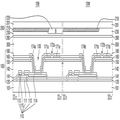
도 2는 도 1의 액정 표시 장치의 임의의 화소들의 평면도이다.
도 3은 도 2의 Ⅲa-Ⅲa' 선을 따라 절개한 단면과, Ⅲb-Ⅲb' 선을 따라 절개한 단면을 비교한 비교단면도이다.
도 4는 도 2의 Ⅳ-Ⅳ' 선을 따라 절개한 단면도이다.
도 5 내지 도 7은 본 발명의 일 실시예에 따른 액정 표시 장치 리페어 방법을 도시한 단면도들이다.
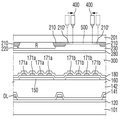
도 8은 본 발명의 다른 실시예에 따른 액정 표시 장치의 단면도이다.
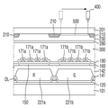
도 9 내지 도 11은 본 발명의 다른 실시예에 따른 액정 표시 장치 리페어 방법을 도시한 단면도들이다.
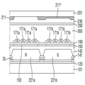
도 12는 본 발명의 또 다른 실시예에 따른 액정 표시 장치의 단면도이다.
도 13 내지 도 15는 본 발명의 또 다른 실시예에 따른 액정 표시 장치 리페어 방법을 도시한 단면도들이다.
도 16 내지 도 17은 본 발명의 또 다른 실시예들에 따른 액정 표시 장치의 단면도들이다.

200 : 제2 기판
210 : 차광 부재
210' : 차광 부재 입자
210'' : 암점화 부재
220 : 컬러 필터
230 : 오버코트층
300 : 액정층
Claims (20)
- 기판, 상기 기판 상에 배치된 차광 부재 및 상기 기판과 상기 차광 부재 상에 배치되며 200 nm 내지 400 nm의 파장을 흡수하는 물질을 함유하는 오버코트층을 포함하는 액정 표시 장치를 제공하는 단계; 및
상기 기판 상의 상기 오버코트층에 200 nm 내지 400 nm의 파장을 갖는 레이저를 조사하여 상기 기판과 상기 오버코트층 사이에 미세 공동을 형성하는 제1 레이저 조사 단계를 포함하는 액정 표시 장치 리페어 방법. - 제1 항에 있어서,
상기 제1 레이저 조사 단계 다음에,
상기 기판 상의 상기 차광 부재에 레이저를 조사하여 상기 차광 부재를 가공하는 제2 레이저 조사 단계를 더 포함하는 액정 표시 장치 리페어 방법. - 제2 항에 있어서,
상기 제2 레이저 조사 단계 다음에,
상기 차광 부재가 가공되어 생성된 차광 부재 입자들을 상기 미세 공동 내로 확산시키는 제3 레이저 조사 단계를 더 포함하는 액정 표시 장치 리페어 방법. - 제3 항에 있어서,
상기 제3 레이저 조사 단계는,
상기 레이저를 상기 차광 부재로부터 상기 차광 부재와 인접한 상기 미세 공동 방향으로 스캔하는 방식으로 조사하는 액정 표시 장치 리페어 방법. - 제1 항에 있어서,
상기 레이저는 450 ps 내지 550 ps의 펄스폭(pulse width)을 갖는 액정 표시 장치 리페어 방법. - 제1 항에 있어서,
상기 200 nm 내지 400 nm의 자외선 파장을 흡수하는 물질은 컨쥬게이션 화합물, 알렌 계열 화합물, 알카인 계열 화합물, 티오에테르기를 포함하는 화합물, 카르보닐 계열 화합물, 에스테르기를 포함하는 화합물, 이민기를 포함하는 화합물, 아조 계열 화합물, 나이트로소기를 포함하는 화합물, 또는 케텐 계열 화합물 중 어느 하나 또는 하나 이상인 액정 표시 장치 리페어 방법. - 기판;
상기 기판 상에 배치되어 제1 화소 영역 및 제2 화소 영역을 포함하는 복수의 화소 영역을 구획하는 제1 차광부;
상기 기판 상의 상기 제1 화소 영역에 배치되는 컬러 필터; 및
상기 기판, 상기 제1 차광부 및 상기 컬러 필터 상에 배치되되, 200 nm 내지 400 nm의 자외선 파장을 흡수하는 물질을 함유하는 오버코트층을 포함하는 액정 표시 장치. - 제7 항에 있어서,
상기 200 nm 내지 400 nm의 자외선 파장을 흡수하는 물질은 컨쥬게이션 화합물, 알렌 계열 화합물, 알카인 계열 화합물, 티오에테르기를 포함하는 화합물, 카르보닐 계열 화합물, 에스테르기를 포함하는 화합물, 이민기를 포함하는 화합물, 아조 계열 화합물, 나이트로소기를 포함하는 화합물, 또는 케텐 계열 화합물 중 어느 하나 또는 하나 이상인 액정 표시 장치. - 제7 항에 있어서,
상기 200 nm 내지 400 nm의 자외선 파장을 흡수하는 물질은 상기 오버코트층을 구성하는 오버코트 조성물 내에서 0.001 wt% 이상 10.0 wt% 이하의 범위로 포함되는 액정 표시 장치. - 제7 항에 있어서,
상기 제2 화소 영역의 적어도 일부와 중첩하는 영역에 형성되며,
상기 기판과 상기 오버코트층 사이에 형성된 미세 공동(micro cavity)을 더 포함하는 액정 표시 장치. - 제10 항에 있어서,
상기 미세 공동 내에 형성되며, 인접한 상기 제1 차광부와 물리적 경계 없이 형성된 제2 차광부를 더 포함하는 액정 표시 장치. - 제1 기판;
상기 제1 기판 상에 배치되어 복수의 화소 영역을 구획하는 제1 차광부; 및
상기 제1 기판 및 상기 제1 차광부 상에 배치되되, 200 nm 내지 400 nm의 자외선 파장을 흡수하는 물질을 함유하는 유기막층을 포함하는 액정 표시 장치. - 제12 항에 있어서,
상기 유기막층 상에 배치되는 컬러 필터를 더 포함하는 액정 표시 장치. - 제13 항에 있어서,
상기 컬러 필터의 적어도 일부와 중첩하는 영역에 형성되며,
상기 제1 기판과 상기 유기막층 사이에 형성된 미세 공동을 더 포함하는 액정 표시 장치. - 제14 항에 있어서,
상기 미세 공동 내에 형성되며, 인접한 제1 차광부와 물리적 경계 없이 형성된 제2 차광부를 더 포함하는 액정 표시 장치. - 제12 항에 있어서,
상기 제1 기판과 이격하여 대향하는 제2 기판; 및
상기 제2 기판 상에 배치되는 컬러 필터를 더 포함하는 액정 표시 장치. - 제16 항에 있어서,
상기 컬러 필터의 적어도 일부와 중첩하는 영역에 형성되며,
상기 제1 기판과 상기 유기막층 사이에 형성된 미세 공동을 더 포함하는 액정 표시 장치. - 제17 항에 있어서,
상기 미세 공동 내에 형성되며, 인접한 제1 차광부와 물리적 경계 없이 형성된 제2 차광부를 더 포함하는 액정 표시 장치. - 제12 항에 있어서,
상기 200 nm 내지 400 nm의 자외선 파장을 흡수하는 물질은 컨쥬게이션 화합물, 알렌 계열 화합물, 알카인 계열 화합물, 티오에테르기를 포함하는 화합물, 카르보닐 계열 화합물, 에스테르기를 포함하는 화합물, 이민기를 포함하는 화합물, 아조 계열 화합물, 나이트로소기를 포함하는 화합물, 또는 케텐 계열 화합물 중 어느 하나 또는 하나 이상인 액정 표시 장치. - 제12 항에 있어서,
상기 200 nm 내지 400 nm의 자외선 파장을 흡수하는 물질은 상기 유기막층을 구성하는 유기막 조성물 내에서 0.001 wt% 이상 10.0 wt% 이하의 범위로 포함되는 액정 표시 장치.
Priority Applications (2)
| Application Number | Priority Date | Filing Date | Title |
|---|---|---|---|
| KR1020150136426A KR102499179B1 (ko) | 2015-09-25 | 2015-09-25 | 액정 표시 장치 및 그 리페어 방법 |
| US14/993,179 US10809550B2 (en) | 2015-09-25 | 2016-01-12 | Liquid crystal display device including first and second light blocking units |
Applications Claiming Priority (1)
| Application Number | Priority Date | Filing Date | Title |
|---|---|---|---|
| KR1020150136426A KR102499179B1 (ko) | 2015-09-25 | 2015-09-25 | 액정 표시 장치 및 그 리페어 방법 |
Publications (2)
| Publication Number | Publication Date |
|---|---|
| KR20170037726A true KR20170037726A (ko) | 2017-04-05 |
| KR102499179B1 KR102499179B1 (ko) | 2023-02-10 |
Family
ID=58408925
Family Applications (1)
| Application Number | Title | Priority Date | Filing Date |
|---|---|---|---|
| KR1020150136426A Active KR102499179B1 (ko) | 2015-09-25 | 2015-09-25 | 액정 표시 장치 및 그 리페어 방법 |
Country Status (2)
| Country | Link |
|---|---|
| US (1) | US10809550B2 (ko) |
| KR (1) | KR102499179B1 (ko) |
Cited By (1)
| Publication number | Priority date | Publication date | Assignee | Title |
|---|---|---|---|---|
| EP3650926A4 (en) * | 2017-07-07 | 2021-03-17 | BOE Technology Group Co., Ltd. | PROCEDURE FOR REPAIRING A DISPLAY BOARD AND DISPLAY BOARD |
Families Citing this family (6)
| Publication number | Priority date | Publication date | Assignee | Title |
|---|---|---|---|---|
| US10600213B2 (en) * | 2016-02-27 | 2020-03-24 | Focal Sharp, Inc. | Method and apparatus for color-preserving spectrum reshape |
| CN107584819B (zh) * | 2017-08-29 | 2019-10-15 | 京东方科技集团股份有限公司 | 一种触控基板及其制作方法、触控装置 |
| TWI692744B (zh) * | 2019-01-25 | 2020-05-01 | 友達光電股份有限公司 | 顯示面板 |
| KR20220041286A (ko) * | 2020-09-24 | 2022-04-01 | 삼성디스플레이 주식회사 | 표시 패널 및 전자 기기 |
| CN112230459B (zh) * | 2020-10-21 | 2024-05-10 | 苏州科韵激光科技有限公司 | 显示面板亮点缺陷修复系统及修复方法 |
| KR20220125104A (ko) * | 2021-03-04 | 2022-09-14 | 삼성전자주식회사 | 표시패널 및 이를 포함하는 전자장치 |
Citations (2)
| Publication number | Priority date | Publication date | Assignee | Title |
|---|---|---|---|---|
| KR20070010876A (ko) * | 2005-07-20 | 2007-01-24 | (주)미래컴퍼니 | 기판 결함 수정장치 및 방법 |
| KR20080111385A (ko) * | 2007-06-18 | 2008-12-23 | 주식회사 코윈디에스티 | 표시장치의 휘점불량 수리방법 |
Family Cites Families (10)
| Publication number | Priority date | Publication date | Assignee | Title |
|---|---|---|---|---|
| KR100778838B1 (ko) * | 2000-12-30 | 2007-11-22 | 엘지.필립스 엘시디 주식회사 | 액정표시장치 및 그 제조방법 |
| KR101299646B1 (ko) * | 2006-10-12 | 2013-08-26 | 삼성디스플레이 주식회사 | 표시패널 및 이의 제조방법 |
| KR101458913B1 (ko) * | 2008-08-05 | 2014-11-07 | 삼성디스플레이 주식회사 | 액정 표시 장치 |
| TWI400540B (zh) * | 2009-09-11 | 2013-07-01 | Hannstar Display Corp | 液晶顯示面板之畫素結構 |
| JP5550357B2 (ja) | 2010-01-15 | 2014-07-16 | 株式会社ジャパンディスプレイ | フロントウインドウ付き表示装置 |
| US8865274B2 (en) * | 2010-04-02 | 2014-10-21 | Samsung Display Co., Ltd. | Liquid crystal display device, alignment film, and methods for manufacturing the same |
| JP5285729B2 (ja) * | 2011-03-03 | 2013-09-11 | 株式会社ジャパンディスプレイ | 液晶表示装置 |
| JP5739217B2 (ja) | 2011-04-22 | 2015-06-24 | 株式会社ジャパンディスプレイ | 液晶表示装置 |
| KR101992884B1 (ko) | 2011-12-21 | 2019-06-26 | 엘지디스플레이 주식회사 | 액정 표시 장치 및 이의 제조 방법 |
| JP6147148B2 (ja) * | 2013-09-03 | 2017-06-14 | 株式会社ジャパンディスプレイ | 配向膜材料およびそれを用いた液晶表示装置 |
-
2015
- 2015-09-25 KR KR1020150136426A patent/KR102499179B1/ko active Active
-
2016
- 2016-01-12 US US14/993,179 patent/US10809550B2/en active Active
Patent Citations (2)
| Publication number | Priority date | Publication date | Assignee | Title |
|---|---|---|---|---|
| KR20070010876A (ko) * | 2005-07-20 | 2007-01-24 | (주)미래컴퍼니 | 기판 결함 수정장치 및 방법 |
| KR20080111385A (ko) * | 2007-06-18 | 2008-12-23 | 주식회사 코윈디에스티 | 표시장치의 휘점불량 수리방법 |
Cited By (2)
| Publication number | Priority date | Publication date | Assignee | Title |
|---|---|---|---|---|
| EP3650926A4 (en) * | 2017-07-07 | 2021-03-17 | BOE Technology Group Co., Ltd. | PROCEDURE FOR REPAIRING A DISPLAY BOARD AND DISPLAY BOARD |
| US11237415B2 (en) | 2017-07-07 | 2022-02-01 | Boe Technology Group Co., Ltd. | Method for repairing a display panel and a display panel |
Also Published As
| Publication number | Publication date |
|---|---|
| US20170090223A1 (en) | 2017-03-30 |
| KR102499179B1 (ko) | 2023-02-10 |
| US10809550B2 (en) | 2020-10-20 |
Similar Documents
| Publication | Publication Date | Title |
|---|---|---|
| KR20170037726A (ko) | 액정 표시 장치 및 그 리페어 방법 | |
| US7733431B2 (en) | Laser repair structure and method for TFT-LCD | |
| US8673104B2 (en) | Fabricating method of liquid crystal display device | |
| US20080220553A1 (en) | Method of producing liquid crystal display device including forming an align mark in an insulating mother substrate | |
| KR20080084034A (ko) | 액정표시장치의 칼라필터 및 제조방법 | |
| CN101600984B (zh) | 液晶显示装置及其制造方法 | |
| KR101473842B1 (ko) | 액정표시패널의 불량셀 리페어방법 | |
| CN101784944B (zh) | 液晶显示装置的制造方法 | |
| JP6714898B2 (ja) | カラーフィルタ基板、およびその製造方法 | |
| WO2016095338A1 (zh) | 铜互连coa型液晶面板暗点修复方法及铜互连coa型液晶面板结构 | |
| JP4354946B2 (ja) | 液晶表示パネル及びそのリペア方法 | |
| US7932983B2 (en) | Method for adjusting amount of liquid crystal in an LCD device including reducing the thickness of a seal member to form a repair region by laser heating a metal pattern thereunder | |
| KR101013647B1 (ko) | 채널부 리페어방법 및 이를 적용한 액정표시소자 | |
| KR100577301B1 (ko) | 액정표시소자 및 그 제조방법 | |
| JP2009128552A (ja) | 液晶表示装置および液晶表示装置の製造方法 | |
| JP2016194624A (ja) | 液晶パネル、液晶表示装置及び、その輝点欠陥修正方法 | |
| CN108254946B (zh) | 显示装置及其制造方法和制造装置 | |
| CN107121795B (zh) | 显示装置及其制造方法和制造装置 | |
| JP4660011B2 (ja) | 液晶表示装置及びその製造方法 | |
| KR101227137B1 (ko) | 액정표시장치의 리페어 장치 및 이를 이용한 리페어 방법 | |
| KR101152555B1 (ko) | 액정패널의 리페어패턴 형성장치 및 방법 | |
| TW201704819A (zh) | 液晶顯示面板及其製造方法 | |
| US10656485B2 (en) | Display device and method for manufacturing the same | |
| WO2008156280A1 (en) | Method of repairing flat pannel display | |
| WO2008156284A1 (en) | Method of repairing flat pannel display |
Legal Events
| Date | Code | Title | Description |
|---|---|---|---|
| PA0109 | Patent application |
Patent event code: PA01091R01D Comment text: Patent Application Patent event date: 20150925 |
|
| PG1501 | Laying open of application | ||
| A201 | Request for examination | ||
| PA0201 | Request for examination |
Patent event code: PA02012R01D Patent event date: 20200903 Comment text: Request for Examination of Application Patent event code: PA02011R01I Patent event date: 20150925 Comment text: Patent Application |
|
| E902 | Notification of reason for refusal | ||
| PE0902 | Notice of grounds for rejection |
Comment text: Notification of reason for refusal Patent event date: 20220420 Patent event code: PE09021S01D |
|
| N231 | Notification of change of applicant | ||
| PN2301 | Change of applicant |
Patent event date: 20220713 Comment text: Notification of Change of Applicant Patent event code: PN23011R01D |
|
| E701 | Decision to grant or registration of patent right | ||
| PE0701 | Decision of registration |
Patent event code: PE07011S01D Comment text: Decision to Grant Registration Patent event date: 20221129 |
|
| GRNT | Written decision to grant | ||
| PR0701 | Registration of establishment |
Comment text: Registration of Establishment Patent event date: 20230208 Patent event code: PR07011E01D |
|
| PR1002 | Payment of registration fee |
Payment date: 20230208 End annual number: 3 Start annual number: 1 |
|
| PG1601 | Publication of registration |