KR20170037726A - Liquid crystal display device and reparing method thereof - Google Patents
Liquid crystal display device and reparing method thereof Download PDFInfo
- Publication number
- KR20170037726A KR20170037726A KR1020150136426A KR20150136426A KR20170037726A KR 20170037726 A KR20170037726 A KR 20170037726A KR 1020150136426 A KR1020150136426 A KR 1020150136426A KR 20150136426 A KR20150136426 A KR 20150136426A KR 20170037726 A KR20170037726 A KR 20170037726A
- Authority
- KR
- South Korea
- Prior art keywords
- substrate
- light
- shielding member
- laser
- liquid crystal
- Prior art date
- Legal status (The legal status is an assumption and is not a legal conclusion. Google has not performed a legal analysis and makes no representation as to the accuracy of the status listed.)
- Granted
Links
- 239000004973 liquid crystal related substance Substances 0.000 title claims abstract description 101
- 238000000034 method Methods 0.000 title claims abstract description 62
- 239000000758 substrate Substances 0.000 claims abstract description 118
- 239000000463 material Substances 0.000 claims abstract description 34
- 230000001678 irradiating effect Effects 0.000 claims abstract description 17
- 150000001875 compounds Chemical class 0.000 claims description 66
- 239000002245 particle Substances 0.000 claims description 24
- 230000008569 process Effects 0.000 claims description 9
- 230000021615 conjugation Effects 0.000 claims description 8
- 239000000203 mixture Substances 0.000 claims description 8
- 125000004185 ester group Chemical group 0.000 claims description 7
- 125000000018 nitroso group Chemical group N(=O)* 0.000 claims description 7
- 150000001361 allenes Chemical class 0.000 claims description 6
- CCGKOQOJPYTBIH-UHFFFAOYSA-N ethenone Chemical compound C=C=O CCGKOQOJPYTBIH-UHFFFAOYSA-N 0.000 claims description 6
- 150000001335 aliphatic alkanes Chemical class 0.000 claims description 5
- 125000002915 carbonyl group Chemical group [*:2]C([*:1])=O 0.000 claims description 5
- 125000000101 thioether group Chemical group 0.000 claims description 5
- 238000000638 solvent extraction Methods 0.000 claims description 4
- 230000007547 defect Effects 0.000 abstract description 25
- 230000008439 repair process Effects 0.000 abstract description 17
- 239000010410 layer Substances 0.000 description 156
- 239000010408 film Substances 0.000 description 40
- 239000004065 semiconductor Substances 0.000 description 13
- 239000010409 thin film Substances 0.000 description 12
- 238000001723 curing Methods 0.000 description 10
- 229910052751 metal Inorganic materials 0.000 description 10
- 239000002184 metal Substances 0.000 description 10
- 230000002950 deficient Effects 0.000 description 9
- 230000001681 protective effect Effects 0.000 description 9
- 230000000903 blocking effect Effects 0.000 description 8
- 238000010304 firing Methods 0.000 description 8
- 239000000126 substance Substances 0.000 description 8
- 239000011230 binding agent Substances 0.000 description 6
- 238000000059 patterning Methods 0.000 description 6
- 239000011347 resin Substances 0.000 description 6
- 229920005989 resin Polymers 0.000 description 6
- -1 azo series compound Chemical class 0.000 description 5
- 230000005684 electric field Effects 0.000 description 5
- 239000000178 monomer Substances 0.000 description 5
- 239000003086 colorant Substances 0.000 description 4
- 125000000879 imine group Chemical group 0.000 description 4
- UHOVQNZJYSORNB-UHFFFAOYSA-N Benzene Chemical compound C1=CC=CC=C1 UHOVQNZJYSORNB-UHFFFAOYSA-N 0.000 description 3
- 239000000654 additive Substances 0.000 description 3
- 239000010949 copper Substances 0.000 description 3
- 238000004519 manufacturing process Methods 0.000 description 3
- 239000012044 organic layer Substances 0.000 description 3
- 239000011368 organic material Substances 0.000 description 3
- 229910052710 silicon Inorganic materials 0.000 description 3
- 239000010936 titanium Substances 0.000 description 3
- KAKZBPTYRLMSJV-UHFFFAOYSA-N Butadiene Chemical compound C=CC=C KAKZBPTYRLMSJV-UHFFFAOYSA-N 0.000 description 2
- RRHGJUQNOFWUDK-UHFFFAOYSA-N Isoprene Chemical compound CC(=C)C=C RRHGJUQNOFWUDK-UHFFFAOYSA-N 0.000 description 2
- 229910052581 Si3N4 Inorganic materials 0.000 description 2
- VYPSYNLAJGMNEJ-UHFFFAOYSA-N Silicium dioxide Chemical compound O=[Si]=O VYPSYNLAJGMNEJ-UHFFFAOYSA-N 0.000 description 2
- XUIMIQQOPSSXEZ-UHFFFAOYSA-N Silicon Chemical compound [Si] XUIMIQQOPSSXEZ-UHFFFAOYSA-N 0.000 description 2
- 206010047571 Visual impairment Diseases 0.000 description 2
- 238000010521 absorption reaction Methods 0.000 description 2
- 230000000996 additive effect Effects 0.000 description 2
- 239000000956 alloy Substances 0.000 description 2
- 125000003277 amino group Chemical group 0.000 description 2
- 229910021417 amorphous silicon Inorganic materials 0.000 description 2
- 238000010000 carbonizing Methods 0.000 description 2
- 125000003178 carboxy group Chemical group [H]OC(*)=O 0.000 description 2
- 239000011651 chromium Substances 0.000 description 2
- 238000011109 contamination Methods 0.000 description 2
- 229910052802 copper Inorganic materials 0.000 description 2
- MGNZXYYWBUKAII-UHFFFAOYSA-N cyclohexa-1,3-diene Chemical compound C1CC=CC=C1 MGNZXYYWBUKAII-UHFFFAOYSA-N 0.000 description 2
- 238000009792 diffusion process Methods 0.000 description 2
- 239000006185 dispersion Substances 0.000 description 2
- 230000000694 effects Effects 0.000 description 2
- 230000004907 flux Effects 0.000 description 2
- 238000007689 inspection Methods 0.000 description 2
- 125000000468 ketone group Chemical group 0.000 description 2
- 239000011159 matrix material Substances 0.000 description 2
- 238000012986 modification Methods 0.000 description 2
- 230000004048 modification Effects 0.000 description 2
- 229910052750 molybdenum Inorganic materials 0.000 description 2
- 239000010703 silicon Substances 0.000 description 2
- HQVNEWCFYHHQES-UHFFFAOYSA-N silicon nitride Chemical compound N12[Si]34N5[Si]62N3[Si]51N64 HQVNEWCFYHHQES-UHFFFAOYSA-N 0.000 description 2
- 229910052814 silicon oxide Inorganic materials 0.000 description 2
- 229910052709 silver Inorganic materials 0.000 description 2
- 239000002904 solvent Substances 0.000 description 2
- 229910052715 tantalum Inorganic materials 0.000 description 2
- 229910052719 titanium Inorganic materials 0.000 description 2
- VXQUABLSXKFKLO-KQQUZDAGSA-N (3e,5e)-octa-1,3,5,7-tetraene Chemical compound C=C\C=C\C=C\C=C VXQUABLSXKFKLO-KQQUZDAGSA-N 0.000 description 1
- AFVDZBIIBXWASR-AATRIKPKSA-N (E)-1,3,5-hexatriene Chemical compound C=C\C=C\C=C AFVDZBIIBXWASR-AATRIKPKSA-N 0.000 description 1
- VYZAMTAEIAYCRO-UHFFFAOYSA-N Chromium Chemical compound [Cr] VYZAMTAEIAYCRO-UHFFFAOYSA-N 0.000 description 1
- RYGMFSIKBFXOCR-UHFFFAOYSA-N Copper Chemical compound [Cu] RYGMFSIKBFXOCR-UHFFFAOYSA-N 0.000 description 1
- ZOKXTWBITQBERF-UHFFFAOYSA-N Molybdenum Chemical compound [Mo] ZOKXTWBITQBERF-UHFFFAOYSA-N 0.000 description 1
- 229910052779 Neodymium Inorganic materials 0.000 description 1
- 229910004205 SiNX Inorganic materials 0.000 description 1
- 229910004286 SiNxOy Inorganic materials 0.000 description 1
- BQCADISMDOOEFD-UHFFFAOYSA-N Silver Chemical compound [Ag] BQCADISMDOOEFD-UHFFFAOYSA-N 0.000 description 1
- RTAQQCXQSZGOHL-UHFFFAOYSA-N Titanium Chemical compound [Ti] RTAQQCXQSZGOHL-UHFFFAOYSA-N 0.000 description 1
- 239000011358 absorbing material Substances 0.000 description 1
- 239000002318 adhesion promoter Substances 0.000 description 1
- 125000003172 aldehyde group Chemical group 0.000 description 1
- 150000001345 alkine derivatives Chemical class 0.000 description 1
- 229910045601 alloy Inorganic materials 0.000 description 1
- 229910052782 aluminium Inorganic materials 0.000 description 1
- XAGFODPZIPBFFR-UHFFFAOYSA-N aluminium Chemical compound [Al] XAGFODPZIPBFFR-UHFFFAOYSA-N 0.000 description 1
- 150000008064 anhydrides Chemical class 0.000 description 1
- FUSUHKVFWTUUBE-UHFFFAOYSA-N buten-2-one Chemical compound CC(=O)C=C FUSUHKVFWTUUBE-UHFFFAOYSA-N 0.000 description 1
- 229910052793 cadmium Inorganic materials 0.000 description 1
- 238000003763 carbonization Methods 0.000 description 1
- 150000001768 cations Chemical class 0.000 description 1
- 239000003795 chemical substances by application Substances 0.000 description 1
- 229910052804 chromium Inorganic materials 0.000 description 1
- HGCIXCUEYOPUTN-UHFFFAOYSA-N cis-cyclohexene Natural products C1CCC=CC1 HGCIXCUEYOPUTN-UHFFFAOYSA-N 0.000 description 1
- 239000011248 coating agent Substances 0.000 description 1
- 238000000576 coating method Methods 0.000 description 1
- 239000000470 constituent Substances 0.000 description 1
- 238000000354 decomposition reaction Methods 0.000 description 1
- 230000006866 deterioration Effects 0.000 description 1
- 125000001033 ether group Chemical group 0.000 description 1
- FONOSWYYBCBQGN-UHFFFAOYSA-N ethylene dione Chemical compound O=C=C=O FONOSWYYBCBQGN-UHFFFAOYSA-N 0.000 description 1
- 125000000524 functional group Chemical group 0.000 description 1
- 229910052732 germanium Inorganic materials 0.000 description 1
- 239000011521 glass Substances 0.000 description 1
- 229910052737 gold Inorganic materials 0.000 description 1
- 238000013007 heat curing Methods 0.000 description 1
- 239000012535 impurity Substances 0.000 description 1
- AMGQUBHHOARCQH-UHFFFAOYSA-N indium;oxotin Chemical compound [In].[Sn]=O AMGQUBHHOARCQH-UHFFFAOYSA-N 0.000 description 1
- 230000001939 inductive effect Effects 0.000 description 1
- 239000003112 inhibitor Substances 0.000 description 1
- 239000003999 initiator Substances 0.000 description 1
- 239000011810 insulating material Substances 0.000 description 1
- 229910052741 iridium Inorganic materials 0.000 description 1
- 229910052742 iron Inorganic materials 0.000 description 1
- XEEYBQQBJWHFJM-UHFFFAOYSA-N iron Substances [Fe] XEEYBQQBJWHFJM-UHFFFAOYSA-N 0.000 description 1
- 239000011733 molybdenum Substances 0.000 description 1
- QEFYFXOXNSNQGX-UHFFFAOYSA-N neodymium atom Chemical compound [Nd] QEFYFXOXNSNQGX-UHFFFAOYSA-N 0.000 description 1
- 230000007935 neutral effect Effects 0.000 description 1
- 229910052759 nickel Inorganic materials 0.000 description 1
- 150000004767 nitrides Chemical class 0.000 description 1
- VXQUABLSXKFKLO-UHFFFAOYSA-N octa-1,3,5,7-tetraene Chemical compound C=CC=CC=CC=C VXQUABLSXKFKLO-UHFFFAOYSA-N 0.000 description 1
- 229910052763 palladium Inorganic materials 0.000 description 1
- 238000002161 passivation Methods 0.000 description 1
- 230000035699 permeability Effects 0.000 description 1
- 238000000016 photochemical curing Methods 0.000 description 1
- 238000001782 photodegradation Methods 0.000 description 1
- 238000007699 photoisomerization reaction Methods 0.000 description 1
- 239000000049 pigment Substances 0.000 description 1
- 239000004033 plastic Substances 0.000 description 1
- 229910052697 platinum Inorganic materials 0.000 description 1
- 230000010287 polarization Effects 0.000 description 1
- 229910021420 polycrystalline silicon Inorganic materials 0.000 description 1
- 238000006116 polymerization reaction Methods 0.000 description 1
- 239000003870 refractory metal Substances 0.000 description 1
- 229910052703 rhodium Inorganic materials 0.000 description 1
- 229910021332 silicide Inorganic materials 0.000 description 1
- FVBUAEGBCNSCDD-UHFFFAOYSA-N silicide(4-) Chemical compound [Si-4] FVBUAEGBCNSCDD-UHFFFAOYSA-N 0.000 description 1
- 239000002210 silicon-based material Substances 0.000 description 1
- 239000004332 silver Substances 0.000 description 1
- 230000000087 stabilizing effect Effects 0.000 description 1
- 239000004094 surface-active agent Substances 0.000 description 1
- GUVRBAGPIYLISA-UHFFFAOYSA-N tantalum atom Chemical compound [Ta] GUVRBAGPIYLISA-UHFFFAOYSA-N 0.000 description 1
- 229920001187 thermosetting polymer Polymers 0.000 description 1
- 150000003568 thioethers Chemical class 0.000 description 1
- WFKWXMTUELFFGS-UHFFFAOYSA-N tungsten Chemical compound [W] WFKWXMTUELFFGS-UHFFFAOYSA-N 0.000 description 1
- 229910052721 tungsten Inorganic materials 0.000 description 1
- 239000010937 tungsten Substances 0.000 description 1
- 229910052725 zinc Inorganic materials 0.000 description 1
- 239000011701 zinc Substances 0.000 description 1
- YVTHLONGBIQYBO-UHFFFAOYSA-N zinc indium(3+) oxygen(2-) Chemical compound [O--].[Zn++].[In+3] YVTHLONGBIQYBO-UHFFFAOYSA-N 0.000 description 1
Images


Classifications
-
- G—PHYSICS
- G02—OPTICS
- G02F—OPTICAL DEVICES OR ARRANGEMENTS FOR THE CONTROL OF LIGHT BY MODIFICATION OF THE OPTICAL PROPERTIES OF THE MEDIA OF THE ELEMENTS INVOLVED THEREIN; NON-LINEAR OPTICS; FREQUENCY-CHANGING OF LIGHT; OPTICAL LOGIC ELEMENTS; OPTICAL ANALOGUE/DIGITAL CONVERTERS
- G02F1/00—Devices or arrangements for the control of the intensity, colour, phase, polarisation or direction of light arriving from an independent light source, e.g. switching, gating or modulating; Non-linear optics
- G02F1/01—Devices or arrangements for the control of the intensity, colour, phase, polarisation or direction of light arriving from an independent light source, e.g. switching, gating or modulating; Non-linear optics for the control of the intensity, phase, polarisation or colour
- G02F1/13—Devices or arrangements for the control of the intensity, colour, phase, polarisation or direction of light arriving from an independent light source, e.g. switching, gating or modulating; Non-linear optics for the control of the intensity, phase, polarisation or colour based on liquid crystals, e.g. single liquid crystal display cells
- G02F1/1306—Details
- G02F1/1309—Repairing; Testing
-
- G—PHYSICS
- G02—OPTICS
- G02B—OPTICAL ELEMENTS, SYSTEMS OR APPARATUS
- G02B5/00—Optical elements other than lenses
- G02B5/20—Filters
- G02B5/208—Filters for use with infrared or ultraviolet radiation, e.g. for separating visible light from infrared and/or ultraviolet radiation
-
- G—PHYSICS
- G02—OPTICS
- G02B—OPTICAL ELEMENTS, SYSTEMS OR APPARATUS
- G02B5/00—Optical elements other than lenses
- G02B5/20—Filters
- G02B5/22—Absorbing filters
- G02B5/223—Absorbing filters containing organic substances, e.g. dyes, inks or pigments
-
- G—PHYSICS
- G02—OPTICS
- G02F—OPTICAL DEVICES OR ARRANGEMENTS FOR THE CONTROL OF LIGHT BY MODIFICATION OF THE OPTICAL PROPERTIES OF THE MEDIA OF THE ELEMENTS INVOLVED THEREIN; NON-LINEAR OPTICS; FREQUENCY-CHANGING OF LIGHT; OPTICAL LOGIC ELEMENTS; OPTICAL ANALOGUE/DIGITAL CONVERTERS
- G02F1/00—Devices or arrangements for the control of the intensity, colour, phase, polarisation or direction of light arriving from an independent light source, e.g. switching, gating or modulating; Non-linear optics
- G02F1/01—Devices or arrangements for the control of the intensity, colour, phase, polarisation or direction of light arriving from an independent light source, e.g. switching, gating or modulating; Non-linear optics for the control of the intensity, phase, polarisation or colour
- G02F1/13—Devices or arrangements for the control of the intensity, colour, phase, polarisation or direction of light arriving from an independent light source, e.g. switching, gating or modulating; Non-linear optics for the control of the intensity, phase, polarisation or colour based on liquid crystals, e.g. single liquid crystal display cells
- G02F1/133—Constructional arrangements; Operation of liquid crystal cells; Circuit arrangements
- G02F1/1333—Constructional arrangements; Manufacturing methods
- G02F1/1335—Structural association of cells with optical devices, e.g. polarisers or reflectors
- G02F1/133509—Filters, e.g. light shielding masks
- G02F1/133512—Light shielding layers, e.g. black matrix
-
- G—PHYSICS
- G02—OPTICS
- G02F—OPTICAL DEVICES OR ARRANGEMENTS FOR THE CONTROL OF LIGHT BY MODIFICATION OF THE OPTICAL PROPERTIES OF THE MEDIA OF THE ELEMENTS INVOLVED THEREIN; NON-LINEAR OPTICS; FREQUENCY-CHANGING OF LIGHT; OPTICAL LOGIC ELEMENTS; OPTICAL ANALOGUE/DIGITAL CONVERTERS
- G02F1/00—Devices or arrangements for the control of the intensity, colour, phase, polarisation or direction of light arriving from an independent light source, e.g. switching, gating or modulating; Non-linear optics
- G02F1/01—Devices or arrangements for the control of the intensity, colour, phase, polarisation or direction of light arriving from an independent light source, e.g. switching, gating or modulating; Non-linear optics for the control of the intensity, phase, polarisation or colour
- G02F1/13—Devices or arrangements for the control of the intensity, colour, phase, polarisation or direction of light arriving from an independent light source, e.g. switching, gating or modulating; Non-linear optics for the control of the intensity, phase, polarisation or colour based on liquid crystals, e.g. single liquid crystal display cells
- G02F1/133—Constructional arrangements; Operation of liquid crystal cells; Circuit arrangements
- G02F1/1333—Constructional arrangements; Manufacturing methods
- G02F1/1335—Structural association of cells with optical devices, e.g. polarisers or reflectors
- G02F1/133509—Filters, e.g. light shielding masks
- G02F1/133514—Colour filters
- G02F1/133519—Overcoatings
-
- G02F2001/133302—
Landscapes
- Physics & Mathematics (AREA)
- Nonlinear Science (AREA)
- General Physics & Mathematics (AREA)
- Optics & Photonics (AREA)
- Chemical & Material Sciences (AREA)
- Crystallography & Structural Chemistry (AREA)
- Mathematical Physics (AREA)
- Health & Medical Sciences (AREA)
- Toxicology (AREA)
- Optical Filters (AREA)
- Inorganic Chemistry (AREA)
- Devices For Indicating Variable Information By Combining Individual Elements (AREA)
- Liquid Crystal (AREA)
Abstract
휘점 결함을 효과적으로 리페어할 수 있는 액정 표시 장치 및 그 리페어 방법이 제공된다. 상기 리페어 방법은 기판, 상기 기판 상에 배치된 차광 부재 및 상기 기판과 상기 차광 부재 상에 배치되며 200 nm 내지 400 nm의 파장을 흡수하는 물질을 함유하는 오버코트층을 포함하는 액정 표시 장치를 제공하는 단계, 및 상기 기판 상의 상기 오버코트층에 200 nm 내지 400 nm의 파장을 갖는 레이저를 조사하여 상기 기판과 상기 오버코트층 사이에 미세 공동을 형성하는 제1 레이저 조사 단계를 포함한다.A liquid crystal display device and a repairing method thereof capable of effectively repairing defocus defects are provided. The repair method includes providing a substrate, a light shielding member disposed on the substrate, and an overcoat layer disposed on the substrate and the light shielding member and containing a material absorbing a wavelength of 200 nm to 400 nm And a first laser irradiation step of irradiating the overcoat layer on the substrate with a laser having a wavelength of 200 nm to 400 nm to form a microcavity between the substrate and the overcoat layer.
Description
본 발명은 액정 표시 장치 및 그 리페어 방법에 관한 것이다.The present invention relates to a liquid crystal display and a repair method thereof.
액정 표시 장치는 현재 가장 널리 사용되고 있는 평판 표시 장치 중 하나로써, 화소 전극과 공통 전극 등 전기장 생성 전극(field generating electrode)이 형성되어 있는 두 장의 기판과 그 사이에 들어 있는 액정층을 포함한다.2. Description of the Related Art [0002] A liquid crystal display device is one of the most widely used flat panel display devices, and includes two substrates on which field generating electrodes such as a pixel electrode and a common electrode are formed, and a liquid crystal layer interposed therebetween.
액정 표시 장치는 전기장 생성 전극에 전압을 인가하여 액정층에 전기장을 생성하고 이를 통하여 액정층의 액정들의 배향 방향을 결정하고 입사광의 편광을 제어함으로써 영상을 표시한다.The liquid crystal display displays an image by applying a voltage to the electric field generating electrode to generate an electric field in the liquid crystal layer, thereby determining the alignment direction of the liquid crystals in the liquid crystal layer and controlling the polarization of the incident light.
한편, 액정 표시 장치를 제조한 후, 액정 표시 장치의 표시 품질을 확인하기 위한 테스트 구동을 하는 경우에 도전성 패턴의 결함 또는 액정층의 결함 등으로 인해 화소가 항상 온(on) 되어 있는 휘점 결함 또는 화소가 항상 오프(off) 되어 있는 암점 결함이 발견될 수 있다.On the other hand, when a test drive for confirming the display quality of a liquid crystal display device is performed after a liquid crystal display device is manufactured, defects such as defects of a conductive pattern or defects of a liquid crystal layer, A dark spot defect in which pixels are always off can be found.
특히 휘점 결함의 경우, 불량이 있는 화소를 암점화 시키는 리페어(repair) 공정을 진행함으로써 상기 휘점 결함으로 인한 표시 품질의 저하를 최소화할 수 있다. 이 같은 불량 화소를 암점화시키는 방법으로 레이저를 이용하여 배선부의 일부를 절단하는 방법이나 액정 표시 장치를 구성하는 베이스 기판 또는 유기막 등을 탄화시키는 방법을 예시할 수 있다. In particular, in the case of defocus defects, it is possible to minimize deterioration of display quality due to the defocus defects by carrying out a repair process of igniting defective pixels. As a method of darkening such defective pixels, a method of cutting a part of a wiring portion using a laser or a method of carbonizing a base substrate or an organic film constituting a liquid crystal display device can be exemplified.
그러나, 레이저를 이용하여 배선부 일부를 절단하는 방법은 성공률이 높지 않을 뿐만 아니라 단락(short)성 화소 결함에 한하여 수행할 수 있기 때문에 그 적용 범위가 넓지 않다. 또한 베이스 기판 또는 유기막 등을 탄화시키는 방법은 액정 표시 장치를 구성하는 구성 요소(예를 들어, 배향막)에 손상이 발생함으로써 이물이 발생하거나 배향력이 저하되고, 이로 인해 빛샘 불량 또는 잔상 불량과 같은 추가적인 불량을 야기할 수 있다.However, the method of cutting a part of the wiring part by using a laser is not only high in the success rate but also applicable to a short pixel defect, so that the application range thereof is not wide. In addition, a method of carbonizing a base substrate, an organic film, or the like causes damage to constituent elements (for example, an alignment film) constituting the liquid crystal display device to cause foreign matter or lower the alignment strength. As a result, And can cause additional defects such as the above.
이에, 본 발명이 해결하고자 하는 과제는 휘점 결함에 광범위하게 적용될 수 있는 새로운 액정 표시 장치 리페어 방법을 제공하는 것이다.SUMMARY OF THE INVENTION Accordingly, it is an object of the present invention to provide a new liquid crystal display repair method that can be widely applied to spots defects.
또, 리페어 공정으로 인한 추가적인 불량을 방지할 수 있는 액정 표시 장치 리페어 방법을 제공하는 것이다.It is another object of the present invention to provide a liquid crystal display repair method capable of preventing further defects due to a repair process.
본 발명이 해결하고자 하는 다른 과제는 휘점 결함이 효과적으로 리페어되어 표시 품질이 향상된 액정 표시 장치를 제공하는 것이다.Another object of the present invention is to provide a liquid crystal display device in which defective defects are effectively repaired and display quality is improved.
본 발명의 과제들은 이상에서 언급한 기술적 과제로 제한되지 않으며, 언급되지 않은 또 다른 기술적 과제들은 아래의 기재로부터 당업자에게 명확하게 이해될 수 있을 것이다.The present invention has been made in view of the above problems, and it is an object of the present invention to provide a method of manufacturing the same.
상기 과제를 해결하기 위한 본 발명의 일 실시예에 따른 액정 표시 장치 리페어 방법은, 기판, 상기 기판 상에 배치된 차광 부재 및 상기 기판과 상기 차광 부재 상에 배치되며 200 nm 내지 400 nm의 파장을 흡수하는 물질을 함유하는 오버코트층을 포함하는 액정 표시 장치를 제공하는 단계, 및 상기 기판 상의 상기 오버코트층에 200 nm 내지 400 nm의 파장을 갖는 레이저를 조사하여 상기 기판과 상기 오버코트층 사이에 미세 공동을 형성하는 제1 레이저 조사 단계를 포함한다.According to an aspect of the present invention, there is provided a method of repairing a liquid crystal display device, the method comprising: providing a substrate, a light shielding member disposed on the substrate, and a light shielding member disposed on the substrate and the light shielding member, And an overcoat layer containing an absorbing material, and irradiating the overcoat layer on the substrate with a laser having a wavelength of 200 nm to 400 nm to form a microcavity between the substrate and the overcoat layer, And a second laser irradiating step of irradiating the first laser beam with the second laser beam.
상기 과제를 해결하기 위한 본 발명의 일 실시예에 따른 액정 표시 장치 리페어 방법에 있어서, 상기 제1 레이저 조사 단계 다음에, 상기 기판 상의 상기 차광 부재에 레이저를 조사하여 상기 차광 부재를 가공하는 제2 레이저 조사 단계를 더 포함할 수 있다.According to another aspect of the present invention, there is provided a method of repairing a liquid crystal display according to an embodiment of the present invention, comprising the steps of: irradiating a laser beam onto the light- And may further include a laser irradiation step.
상기 과제를 해결하기 위한 본 발명의 일 실시예에 따른 액정 표시 장치 리페어 방법에 있어서, 상기 제2 레이저 조사 단계 다음에, 상기 차광 부재가 가공되어 생성된 차광 부재 입자들을 상기 미세 공동 내로 확산시키는 제3 레이저 조사 단계를 더 포함할 수 있다.According to another aspect of the present invention, there is provided a method for repairing a liquid crystal display according to an embodiment of the present invention, comprising the steps of: irradiating the light shielding member with light, 3 laser irradiation step.
상기 과제를 해결하기 위한 본 발명의 일 실시예에 따른 액정 표시 장치 리페어 방법에 있어서, 상기 제3 레이저 조사 단계는, 상기 레이저를 상기 차광 부재로부터 상기 차광 부재와 인접한 상기 미세 공동 방향으로 스캔하는 방식으로 조사할 수 있다.According to another aspect of the present invention, there is provided a method of repairing a liquid crystal display according to an embodiment of the present invention, wherein the third laser irradiating step includes a step of scanning the laser from the light shielding member toward the micro- .
상기 과제를 해결하기 위한 본 발명의 일 실시예에 따른 액정 표시 장치 리페어 방법에 있어서, 상기 레이저는 450 ps 내지 550 ps의 펄스폭(pulse width)을 가질 수 있다.According to an aspect of the present invention, there is provided a method of repairing a liquid crystal display (LCD) device, the laser having a pulse width of 450 ps to 550 ps.
상기 과제를 해결하기 위한 본 발명의 일 실시예에 따른 액정 표시 장치 리페어 방법에 있어서, 상기 200 nm 내지 400 nm의 자외선 파장을 흡수하는 물질은 컨쥬게이션 화합물, 알렌 계열 화합물, 알카인 계열 화합물, 티오에테르기를 포함하는 화합물, 카르보닐 계열 화합물, 에스테르기를 포함하는 화합물, 이민기를 포함하는 화합물, 아조 계열 화합물, 나이트로소기를 포함하는 화합물, 또는 케텐 계열 화합물 중 어느 하나 또는 하나 이상일 수 있다.According to an embodiment of the present invention, there is provided a method of repairing a liquid crystal display according to an embodiment of the present invention, wherein the material absorbing the ultraviolet light having a wavelength of 200 nm to 400 nm is selected from the group consisting of conjugation compounds, allene- An ether group-containing compound, a carbonyl-based compound, an ester group-containing compound, an imine group-containing compound, an azo series compound, a nitroso group-containing compound, or a ketene series compound.
상기 과제를 해결하기 위한 본 발명의 일 실시예에 따른 액정 표시 장치는, 기판, 상기 기판 상에 배치되어 제1 화소 영역 및 제2 화소 영역을 포함하는 복수의 화소 영역을 구획하는 제1 차광부, 상기 기판 상의 상기 제1 화소 영역에 배치되는 컬러 필터, 및 상기 기판, 상기 제1 차광부 및 상기 컬러 필터 상에 배치되되, 200 nm 내지 400 nm의 자외선 파장을 흡수하는 물질을 함유하는 오버코트층을 포함한다.According to an aspect of the present invention, there is provided a liquid crystal display device including a substrate, a first light-shielding part arranged on the substrate and partitioning a plurality of pixel areas including a first pixel area and a second pixel area, A color filter disposed in the first pixel region on the substrate, and a color filter disposed on the substrate, the first light-shielding portion, and the color filter, wherein the overcoat layer contains a substance absorbing an ultraviolet wavelength of 200 nm to 400 nm .
상기 과제를 해결하기 위한 본 발명의 일 실시예에 따른 액정 표시 장치에 있어서, 상기 200 nm 내지 400 nm의 자외선 파장을 흡수하는 물질은 컨쥬게이션 화합물, 알렌 계열 화합물, 알카인 계열 화합물, 티오에테르기를 포함하는 화합물, 카르보닐 계열 화합물, 에스테르기를 포함하는 화합물, 이민기를 포함하는 화합물, 아조 계열 화합물, 나이트로소기를 포함하는 화합물, 또는 케텐 계열 화합물 중 어느 하나 또는 하나 이상일 수 있다.In order to solve the above problems, the liquid crystal display according to an embodiment of the present invention may include a conjugation compound, an allene-based compound, an alkane-based compound, a thioether group, , A compound containing an amino group, a compound containing a carboxyl group, a compound containing an ester group, a compound containing an imine group, an azo compound, a compound containing a nitroso group, or a ketene-based compound.
상기 과제를 해결하기 위한 본 발명의 일 실시예에 따른 액정 표시 장치에 있어서, 상기 200 nm 내지 400 nm의 자외선 파장을 흡수하는 물질은 상기 오버코트층을 구성하는 오버코트 조성물 내에서 0.001 wt% 이상 10.0 wt% 이하의 범위로 포함될 수 있다.In the liquid crystal display according to an embodiment of the present invention for solving the above problems, the material absorbing the ultraviolet light having a wavelength of 200 nm to 400 nm is contained in the overcoat composition constituting the overcoat layer in an amount of 0.001 wt% to 10.0 wt % ≪ / RTI >
상기 과제를 해결하기 위한 본 발명의 일 실시예에 따른 액정 표시 장치에 있어서, 상기 제2 화소 영역의 적어도 일부와 중첩하는 영역에 형성되며, 상기 기판과 상기 오버코트층 사이에 형성된 미세 공동(micro cavity)을 더 포함할 수 있다.According to an aspect of the present invention, there is provided a liquid crystal display device comprising: a micro-cavity formed between a substrate and an overcoat layer, the micro-cavity being formed in a region overlapping at least a part of the second pixel region; ). ≪ / RTI >
상기 과제를 해결하기 위한 본 발명의 일 실시예에 따른 액정 표시 장치에 있어서, 상기 미세 공동 내에 형성되며, 인접한 상기 제1 차광부와 물리적 경계 없이 형성된 제2 차광부를 더 포함할 수 있다.The liquid crystal display according to an embodiment of the present invention may further include a second light blocking part formed in the microcavity and formed without a physical boundary with the adjacent first light blocking part.
상기 과제를 해결하기 위한 본 발명의 다른 실시예에 따른 액정 표시 장치는, 제1 기판, 상기 제1 기판 상에 배치되어 복수의 화소 영역을 구획하는 제1 차광부, 및 상기 제1 기판 및 상기 제1 차광부 상에 배치되되, 200 nm 내지 400 nm의 자외선 파장을 흡수하는 물질을 함유하는 유기막층을 포함한다.According to another aspect of the present invention, there is provided a liquid crystal display device including a first substrate, a first light-shielding portion disposed on the first substrate and partitioning a plurality of pixel regions, And an organic film layer disposed on the first light-emitting portion and containing a substance absorbing an ultraviolet wavelength of 200 nm to 400 nm.
상기 과제를 해결하기 위한 본 발명의 다른 실시예에 따른 액정 표시 장치에 있어서, 상기 유기막층 상에 배치되는 컬러 필터를 더 포함할 수 있다.The liquid crystal display according to another embodiment of the present invention may further include a color filter disposed on the organic layer.
상기 과제를 해결하기 위한 본 발명의 다른 실시예에 따른 액정 표시 장치에 있어서, 상기 컬러 필터의 적어도 일부와 중첩하는 영역에 형성되며, 상기 제1 기판과 상기 유기막층 사이에 형성된 미세 공동을 더 포함할 수 있다.According to another aspect of the present invention, there is provided a liquid crystal display device including a microcavity formed in an area overlapping at least a part of the color filter, the microcavity being formed between the first substrate and the organic layer can do.
상기 과제를 해결하기 위한 본 발명의 다른 실시예에 따른 액정 표시 장치에 있어서, 상기 미세 공동 내에 형성되며, 인접한 제1 차광부와 물리적 경계 없이 형성된 제2 차광부를 더 포함할 수 있다.The liquid crystal display according to another embodiment of the present invention may further include a second light shielding part formed in the microcavity and formed without a physical boundary with the adjacent first light blocking part.
상기 과제를 해결하기 위한 본 발명의 다른 실시예에 따른 액정 표시 장치에 있어서, 상기 제1 기판과 이격하여 대향하는 제2 기판, 및 상기 제2 기판 상에 배치되는 컬러 필터를 더 포함할 수 있다.According to another aspect of the present invention, there is provided a liquid crystal display device including a second substrate facing a first substrate and spaced apart from the first substrate, and a color filter disposed on the second substrate. .
상기 과제를 해결하기 위한 본 발명의 다른 실시예에 따른 액정 표시 장치에 있어서, 상기 컬러 필터의 적어도 일부와 중첩하는 영역에 형성되며, 상기 제1 기판과 상기 유기막층 사이에 형성된 미세 공동을 더 포함할 수 있다.According to another aspect of the present invention, there is provided a liquid crystal display device including a microcavity formed in an area overlapping at least a part of the color filter, the microcavity being formed between the first substrate and the organic layer can do.
상기 과제를 해결하기 위한 본 발명의 다른 실시예에 따른 액정 표시 장치에 있어서, 상기 미세 공동 내에 형성되며, 인접한 제1 차광부와 물리적 경계 없이 형성된 제2 차광부를 더 포함할 수 있다.The liquid crystal display according to another embodiment of the present invention may further include a second light shielding part formed in the microcavity and formed without a physical boundary with the adjacent first light blocking part.
상기 과제를 해결하기 위한 본 발명의 다른 실시예에 따른 액정 표시 장치에 있어서, 상기 200 nm 내지 400 nm의 자외선 파장을 흡수하는 물질은 컨쥬게이션 화합물, 알렌 계열 화합물, 알카인 계열 화합물, 티오에테르기를 포함하는 화합물, 카르보닐 계열 화합물, 에스테르기를 포함하는 화합물, 이민기를 포함하는 화합물, 아조 계열 화합물, 나이트로소기를 포함하는 화합물, 또는 케텐 계열 화합물 중 어느 하나 또는 하나 이상일 수 있다.In the liquid crystal display according to another embodiment of the present invention for solving the above problems, the substance absorbing the ultraviolet light having a wavelength of 200 nm to 400 nm may be a conjugation compound, an allene-based compound, an alkane-based compound or a thioether group , A compound containing an amino group, a compound containing a carboxyl group, a compound containing an ester group, a compound containing an imine group, an azo compound, a compound containing a nitroso group, or a ketene-based compound.
상기 과제를 해결하기 위한 본 발명의 다른 실시예에 따른 액정 표시 장치에 있어서, 상기 200 nm 내지 400 nm의 자외선 파장을 흡수하는 물질은 상기 유기막층을 구성하는 유기막 조성물 내에서 0.001 wt% 이상 10.0 wt% 이하의 범위로 포함될 수 있다.In the liquid crystal display device according to another embodiment of the present invention for solving the above problems, the substance absorbing the ultraviolet light having a wavelength of 200 nm to 400 nm is contained in the organic film composition constituting the organic film layer in an amount of 0.001 wt% wt% or less.
기타 실시예의 구체적인 사항들은 상세한 설명 및 도면들에 포함되어 있다.The details of other embodiments are included in the detailed description and drawings.
본 발명의 일 실시예에 따른 액정 표시 장치 리페어 방법에 의하면, 휘점 결함이 발생한 화소의 화소 영역의 오버코트층에 미세공동(micro cavity)을 형성하고, 상기 미세공동 내에 차광 물질을 충진시킴으로써 광 경로를 효과적으로 차단할 수 있다.According to the method for repairing a liquid crystal display device according to an embodiment of the present invention, a micro cavity is formed in the overcoat layer of a pixel region of a pixel where a spot defect occurs, and a light shielding material is filled in the microcavity, It can be effectively blocked.
또, 화소 영역이 표시하는 색에 따라 리페어 공정에 사용되는 레이저의 파장이 달라지지 않기 때문에 리페어 설비를 단일화할 수 있고, 공정성을 개선할 수 있으며, 액정 표시 장치의 생성 수율을 향상시킬 수 있다.In addition, since the wavelength of the laser used in the repair process is not changed according to the color displayed by the pixel region, the repair facility can be unified, the processability can be improved, and the production yield of the liquid crystal display device can be improved.
또한, 리페어 공정 중에 이물이 발생하지 않기 때문에 이물이 액정층 내로 유입되는 등의 문제를 미연에 방지할 수 있다.In addition, since no foreign matter is generated during the repairing process, problems such as the inflow of foreign matter into the liquid crystal layer can be prevented in advance.
본 발명의 일 실시예에 따른 액정 표시 장치에 의하면, 휘점 결함이 효과적으로 리페어된 액정 표시 장치를 제공함으로써 표시 품질이 개선될 수 있다.According to the liquid crystal display device according to an embodiment of the present invention, the display quality can be improved by providing the liquid crystal display device in which the defective spot defects are effectively repaired.
본 발명의 실시예들에 따른 효과는 이상에서 예시된 내용에 의해 제한되지 않으며, 더욱 다양한 효과들이 본 명세서 내에 포함되어 있다.The effects according to the embodiments of the present invention are not limited by the contents exemplified above, and more various effects are included in the specification.
도 1은 본 발명의 일 실시예에 따른 액정 표시 장치의 분해사시도이다.
도 2는 도 1의 액정 표시 장치의 임의의 화소들의 평면도이다.
도 3은 도 2의 Ⅲa-Ⅲa' 선을 따라 절개한 단면과, Ⅲb-Ⅲb' 선을 따라 절개한 단면을 비교한 비교단면도이다.
도 4는 도 2의 Ⅳ-Ⅳ' 선을 따라 절개한 단면도이다.
도 5 내지 도 7은 본 발명의 일 실시예에 따른 액정 표시 장치 리페어 방법을 도시한 단면도들이다.
도 8은 본 발명의 다른 실시예에 따른 액정 표시 장치의 단면도이다.
도 9 내지 도 11은 본 발명의 다른 실시예에 따른 액정 표시 장치 리페어 방법을 도시한 단면도들이다.
도 12는 본 발명의 또 다른 실시예에 따른 액정 표시 장치의 단면도이다.
도 13 내지 도 15는 본 발명의 또 다른 실시예에 따른 액정 표시 장치 리페어 방법을 도시한 단면도들이다.
도 16 내지 도 17은 본 발명의 또 다른 실시예들에 따른 액정 표시 장치의 단면도들이다.1 is an exploded perspective view of a liquid crystal display device according to an embodiment of the present invention.
2 is a plan view of arbitrary pixels of the liquid crystal display device of FIG.
FIG. 3 is a cross-sectional view illustrating a cross-section taken along line IIIa-IIIa of FIG. 2 and a cross-section taken along line IIIb-IIIb of FIG.
4 is a cross-sectional view taken along the line IV-IV 'of FIG.
5 to 7 are sectional views illustrating a liquid crystal display repair method according to an embodiment of the present invention.
8 is a cross-sectional view of a liquid crystal display device according to another embodiment of the present invention.
9 to 11 are cross-sectional views illustrating a liquid crystal display repair method according to another embodiment of the present invention.
12 is a cross-sectional view of a liquid crystal display device according to another embodiment of the present invention.
13 to 15 are sectional views illustrating a liquid crystal display repair method according to another embodiment of the present invention.
16 to 17 are sectional views of a liquid crystal display according to still another embodiment of the present invention.
본 발명의 이점 및 특징, 그리고 그것들을 달성하는 방법은 첨부되는 도면과 함께 상세하게 후술되어 있는 실시예들을 참조하면 명확해질 것이다.BRIEF DESCRIPTION OF THE DRAWINGS The advantages and features of the present invention and the manner of achieving them will become apparent with reference to the embodiments described in detail below with reference to the accompanying drawings.
그러나 본 발명은 이하에서 개시되는 실시예들에 한정되는 것이 아니라 서로 다른 다양한 형태로 구현될 것이며, 단지 실시예들은 본 발명의 개시가 완전하도록 하며, 본 발명이 속하는 기술분야에서 통상의 지식을 가진 자에게 발명의 범주를 완전하게 알려주기 위해 제공되는 것이며, 본 발명은 청구항의 범주에 의해 정의될 뿐이다.The present invention will now be described more fully hereinafter with reference to the accompanying drawings, in which preferred embodiments of the invention are shown. However, it will be understood by those of ordinary skill in the art that various changes in form and details may be made therein without departing from the spirit and scope of the invention. To fully disclose the scope of the invention to a person skilled in the art, and the invention is only defined by the scope of the claims.
공간적으로 상대적인 용어인 "아래(below)", "아래(beneath)", "하부(lower)", "위(above)", "상부(upper)" 등은 도면에 도시되어 있는 바와 같이 하나의 소자 또는 구성 요소들과 다른 소자 또는 구성 요소들과의 상관관계를 용이하게 기술하기 위해 사용될 수 있다. 공간적으로 상대적인 용어는 도면에 도시되어 있는 방향에 더하여 사용시 소자의 서로 다른 방향을 포함하는 용어로 이해되어야 한다. 예를 들면, 도면에 도시되어 있는 소자를 뒤집을 경우, 다른 소자의 "아래(below 또는 beneath)"로 기술된 소자는 다른 소자의 "위(above)"에 놓여질 수 있다. 따라서, 예시적인 용어인 "아래"는 아래와 위의 방향을 모두 포함할 수 있다.The terms spatially relative, "below", "beneath", "lower", "above", "upper" May be used to readily describe a device or a relationship of components to other devices or components. Spatially relative terms should be understood to include terms in different directions of the device in use, in addition to the directions shown in the figures. For example, when inverting an element shown in the figure, an element described as " below or beneath "of another element may be placed" above "another element. Thus, the exemplary term "below" can include both downward and upward directions.
이하, 첨부된 도면을 참고로 하여 본 발명의 실시예들에 대하여 설명한다.Hereinafter, embodiments of the present invention will be described with reference to the accompanying drawings.
도 1은 본 발명의 일 실시예에 따른 액정 표시 장치의 분해사시도이다.1 is an exploded perspective view of a liquid crystal display device according to an embodiment of the present invention.
도 1을 참조하면, 본 발명의 일 실시예에 따른 액정 표시 장치는 제1 기판(100), 제1 기판(100)과 이격하여 대향하는 제2 기판(200) 및 제1 기판(100)과 제2 기판(200) 사이에 개재되는 액정층(300)을 포함한다. 제1 기판(100)은 하부 기판이고, 제2 기판(200)은 상부 기판일 수 있다.1, a liquid crystal display according to an exemplary embodiment of the present invention includes a
제1 기판(100) 및 제2 기판(200)은 각각 표시 영역(DA) 및 비표시영역(NA)을 포함한다. 표시영역(DA)은 화상이 시인되는 영역이고, 비표시영역(NA)은 화상이 시인되지 않는 영역이다. 표시영역(DA)은 외곽이 비표시영역(NA)으로 둘러싸여 있다.The
표시영역(DA)은 제1 방향(X1, 행 방향)으로 연장된 복수의 게이트 라인(GL), 제1 방향(X1)과 교차하는 제2 방향(X2, 열 방향)으로 연장된 복수의 데이터 라인(DL) 및 게이트 라인(GL)과 데이터 라인(DL)이 교차하는 영역에 형성된 복수의 화소 영역(PX)들을 포함한다. 복수의 화소 영역(PX)들은 제1 방향(X1) 및 제2 방향(X2)으로 배열되어 실질적으로 매트릭스 형상으로 배치될 수 있다.The display area DA includes a plurality of gate lines GL extending in a first direction X1 (row direction), a plurality of data lines DL extending in a second direction X2 (column direction) intersecting the first direction X1 And a plurality of pixel regions PX formed in regions where the lines DL and the gate lines GL intersect with the data lines DL. The plurality of pixel regions PX may be arranged in a first direction X1 and a second direction X2 and arranged substantially in a matrix form.
각 화소 영역(PX)들은 색 표시를 구현하기 위해서 기본색(primary color) 중 하나의 색상을 고유하게 표시할 수 있다. 상기 기본색의 예로는 적색(red), 녹색(green), 청색(blue) 및 백색(white)을 들 수 있다. 본 명세서에서, 적색을 표시하는 화소 영역을 적색 화소(R), 녹색을 표시하는 화소 영역을 녹색 화소(G), 청색을 표시하는 화소 영역 청색 화소(B), 백색을 표시하는 화소 영역을 백색 화소(W)라 한다.Each pixel region PX may uniquely display one of the primary colors to implement the color display. Examples of the basic colors include red, green, blue, and white. In this specification, a pixel region displaying red is referred to as a red pixel R, a pixel region displaying green is referred to as a green pixel (G), a pixel region blue pixel (B) displaying a blue color, (W).
본 실시예에 따른 액정 표시 장치는 적색 화소(R), 녹색 화소(G), 청색 화소(B) 및 백색 화소(W)를 포함할 수 있다. 구체적으로, 도 1에 도시된 바와 같이 적색 화소(R), 녹색 화소(G), 청색 화소(B) 및 백색 화소(W)가 기본 단위를 이루어 제1 방향(행 방향)을 따라 반복 배치되며, 홀수 번째 열은 적색 화소(R)와 청색 화소(B)가 기본 단위를 이루고, 짝수 번째 열은 녹색 화소(G)와 백색 화소(W)가 기본 단위를 이루어 제2 방향(열 방향)을 따라 반복 배치되며, 적색 화소(R), 녹색 화소(G), 청색 화소(B) 및 백색 화소(W)가 2 X 2 로 배치되어 하나의 도트(dot)를 형성하는 화소 배열 구조를 가질 수 있으나 이에 제한되는 것은 아니며, 다양한 RGBW 배열 구조를 가질 수도 있다.The liquid crystal display device according to the present embodiment may include a red pixel R, a green pixel G, a blue pixel B, and a white pixel W. Specifically, as shown in FIG. 1, red pixels R, green pixels G, blue pixels B, and white pixels W are repeatedly arranged along a first direction (row direction) in a basic unit , The odd-numbered columns constitute the basic units of the red pixel R and the blue pixel B, and the even-numbered columns constitute the basic unit of the green pixel G and the white pixel W, And may have a pixel array structure in which a red pixel R, a green pixel G, a blue pixel B and a white pixel W are arranged in 2 X 2 to form one dot However, the present invention is not limited thereto, and it may have various RGBW array structures.
비표시영역(NA)은 차광 영역일 수 있다. 제1 기판(100)의 비표시영역(NA)에는 표시영역(DA)의 화소들에 게이트 구동 신호, 데이터 구동 신호 등을 제공하는 구동부(미도시)가 배치될 수 있다. 게이트 라인(GL)들과 데이터 라인(DL)들은 표시영역(DA)으로부터 비표시영역(NA)까지 연장되어 구동부(미도시)와 전기적으로 연결될 수 있다.The non-display area NA may be a light shielding area. A driving unit (not shown) may be disposed in the non-display area NA of the
제1 기판(100)과 제2 기판(200) 사이에는 액정층(300)이 개재될 수 있다. 액정층(300)은 양의 유전율 이방성을 갖는 액정 분자들을 포함할 수 있으나, 이에 제한되지 않고 음의 유전율 이방성을 갖는 액정 분자들을 포함할 수도 있다.A
이하, 본 발명의 일 실시예에 따른 액정 표시 장치의 화소 영역에 대해 상세하게 설명한다.Hereinafter, a pixel region of a liquid crystal display device according to an embodiment of the present invention will be described in detail.
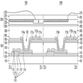
도 2는 도 1의 액정 표시 장치의 청색을 표시하는 제1 화소(10B)와 백색을 표시하는 제2 화소(10W)의 평면도이다. 도 3은 도 2의 Ⅲa-Ⅲa' 선을 따라 절개한 단면과, Ⅲb-Ⅲb' 선을 따라 절개한 단면을 비교한 비교단면도이다. 도 4는 도 2의 Ⅳ-Ⅳ' 선을 따라 절개한 단면도이다.2 is a plan view of a
도 2 내지 도 4를 참조하면, 제1 기판(100)은 제1 베이스 기판(101), 복수의 박막 트랜지스터(110), 공통 전극(150), 제1 화소 전극(170a), 제2 화소 전극(170b), 제1 배향막(180) 및 복수의 보호막/절연막 등을 포함할 수 있다.2 to 4, the
제1 베이스 기판(101)은 투명한 절연 기판으로 투과성, 내열성, 내화학성 등이 우수한 물질로 형성될 수 있다. 예를 들어, 제1 베이스 기판(101)은 실리콘 기판, 유리 기판 또는 플라스틱 기판 등일 수 있다.The
제1 베이스 기판(101) 상에는 게이트 배선층이 배치된다. 상기 게이트 배선층은 게이트 라인(GL) 및 게이트 전극(111)을 포함한다.A gate wiring layer is disposed on the
게이트 라인(GL)은 대략 제1 방향(X1)을 따라 연장된다. 게이트 전극(111)은 게이트 라인(GL)으로부터 상측으로 돌출되어 서로 물리적 경계 없이 일체로 형성될 수 있다. 게이트 전극(111)에는 게이트 라인(GL)으로부터 제공된 게이트 신호가 인가될 수 있다. 상기 게이트 배선층은 탄탈륨(Ta), 텅스텐(W), 티타늄(Ti), 몰리브덴(Mo), 알루미늄(Al), 구리(Cu), 은(Ag), 크롬(Cr) 또는 네오듐(Nd)으로부터 선택된 원소 또는 그 원소를 주성분으로 하는 합금 재료 또는 화합물 재료를 포함하는 제1 금속층을 형성한 후 상기 제1 금속층을 패터닝하여 형성할 수 있다. 상기 패터닝은 마스크 공정을 이용할 수 있으며, 이외에도 패턴을 형성할 수 있는 다른 방법을 이용하여도 무방하다.The gate line GL extends substantially along the first direction X1. The
상기 게이트 배선층 상에는 제1 베이스 기판(101) 전면에 걸쳐 게이트 절연막(120)이 배치된다. 게이트 절연막(120)은 절연 물질로 구성되어 그 상부에 위치하는 층과 하부에 위치하는 층을 서로 전기적으로 절연시킬 수 있다. 게이트 절연막(120)을 형성하는 물질의 예로는 질화규소(SiNx), 산화규소(SiOx) 질화산화규소(SiNxOy) 또는 산화질화규소(SiOxNy) 등을 들 수 있으며, 물리적 성질이 다른 적어도 두 개의 절연층을 포함하는 다층막 구조로 형성될 수도 있다.A
게이트 절연막(120) 상에는 반도체층(112)이 배치된다. 반도체층(112)의 적어도 일부는 게이트 전극(111)과 중첩되는 영역에 배치된다. 반도체층(112)은 박막 트랜지스터(110)의 채널(channel) 역할을 수행하며, 게이트 전극에 제공되는 전압에 따라 채널을 턴온(turn on) 또는 턴오프(turn off) 할 수 있다. 반도체층(112)은 비정질 실리콘, 다결정 실리콘 또는 산화물 반도체 등과 같은 반도체 물질을 포함하는 반도체 물질층을 패터닝하여 형성할 수 있다.A
반도체층(112) 상부에는 데이터 배선층이 배치된다. 상기 데이터 배선층은 데이터 라인(DL), 소스 전극(113) 및 드레인 전극(114)을 포함할 수 있다.A data wiring layer is disposed on the
데이터 라인(DL)은 대략 제2 방향(X2)을 따라 연장되어 게이트 라인(GL)을 교차한다. 데이터 라인(DL)에는 데이터 신호가 인가될 수 있다. 데이터 라인(DL)과 게이트 라인(GL)이 교차하는 영역은 화소 영역이 정의된다. 복수의 각 화소 영역은 대응하는 게이트 라인(GL)과 데이터 라인(DL)에 의해 연결된 복수의 박막 트랜지스터(110)들에 의해 독립적으로 동작되는 영역일 수 있다.The data line DL extends substantially in the second direction X2 and crosses the gate line GL. A data signal may be applied to the data line DL. An area where the data line DL and the gate line GL intersect is defined as a pixel area. Each of the plurality of pixel regions may be an area independently operated by a plurality of
소스 전극(113)과 드레인 전극(114)은 게이트 전극(111)과 반도체층(112) 상에서 서로 이격되어 배치된다. 소스 전극(113)은 데이터 라인(DL)과 물리적 경계 없이 일체로 형성될 수 있다. 도 2는 소스 전극(113)이 데이터 라인(DL)의 일부분인 경우가 예시되지만, 소스 전극은 데이터 라인으로부터 게이트 전극 방향으로 돌출되도록 형성될 수도 있다. 드레인 전극(114)은 후술할 컨택홀(130)을 통해 화소 전극(170a)과 전기적으로 연결된다.The
상기 데이터 배선층은 은(Ag), 금(Au), 구리(Cu), 니켈(Ni), 백금(Pt), 팔라듐(Pd), 이리듐(Ir), 로듐(Rh), 텅스텐(W), 알루미늄(Al), 탄탈륨(Ta), 몰리브덴(Mo), 카드뮴(Cd), 아연(Zn), 철(Fe), 티타늄(Ti), 규소(Si), 게르마늄(Ge), 지르코늄(Zr) 또는 바륨(Ba) 등의 내화성 금속(refractory metal) 또는 그 합금 또는 그 금속 질화물을 포함하는 제2 금속층을 형성한 후 상기 제2 금속층을 패터닝하여 형성할 수 있다.The data wiring layer may be formed of at least one selected from the group consisting of Ag, Au, Cu, Ni, Pt, Pd, Ir, Rh, (Al), Ta, Mo, Cd, Zn, Fe, Ti, Si, Ge, A refractory metal such as Ba, or an alloy thereof, or a metal nitride thereof, and then patterning the second metal layer.
반도체층(112)과 상기 데이터 배선층 사이에는 오믹 컨택층(115)이 배치될 수 있다. 오믹 컨택층(115)은 n형 불순물이 고농도로 도핑되어 있는 n+ 수소화 비정질 실리콘 물질을 포함하거나, 실리사이드(silicide)를 포함할 수 있다.An
전술한 게이트 전극(111), 반도체층(112), 소스 전극(113) 및 드레인 전극(114)은 삼단자 소자인 박막 트랜지스터(110)를 구성한다. 구체적으로, 박막 트랜지스터의 제어 단자인 게이트 전극(111)은 게이트 라인(GL)과 물리적으로 연결되고, 반도체층(112)은 박막 트랜지스터의 채널 역할을 수행하며, 입력 단자인 소스 전극(113)은 데이터 라인(DL)과 물리적으로 연결되며, 출력 단자인 드레인 전극(114)은 제1 화소 전극(170a)과 전기적으로 연결된다.The
상기 데이터 배선층 상에는 제1 베이스 기판(101) 전면에 걸쳐 보호막(141)이 배치된다. 보호막(141)은 유기막 및/또는 무기막으로 형성될 수 있으며, 단일막 또는 다중막 구조를 가질 수도 있다. 보호막(141)은 하부에 형성된 배선들 및 박막 트랜지스터(110)의 반도체층(112)이 노출되어 유기 물질과 직접 접촉하는 것을 방지할 수 있다.On the data wiring layer, a
보호막(141) 상에는 전면에 걸쳐 제1 절연층(142)이 배치된다. 제1 절연층(142)은 유기 물질을 포함하여 이루어질 수 있다. 제1 절연층(142)은 제1 베이스 기판(101) 상에 적층된 복수의 구성 요소의 높이를 균일하게 만들 수 있다.A first insulating
제1 절연층(142) 상에는 공통 전극(150)이 배치될 수 있다. 공통 전극(150)은 제3 금속층을 패터닝하여 형성된 투명 전극일 수 있다. 상기 제3 금속층을 형성하는 물질의 예로는 인듐 틴 옥사이드(indium tin oxide, ITO), 인듐 징크 옥사이드(indium zinc oxide) 등을 들 수 있으나 이에 제한되지 않는다. 공통 전극(150)은 후술할 제1 및 제2 화소 전극(170a, 170b)과 함께 프린지 전계(fringe field)를 형성하여 액정층(300) 내 액정 분자들을 제어할 수 있다. 공통 전극(150)은 각 화소 영역(10B, 10W)에서 일부 영역을 제외한 대부분의 영역과 중첩되어 배치될 수 있다. 공통 전극(150) 상에는 제2 절연층(160)이 배치되며, 하부의 공통 전극(150)과 상부의 제1 및 제2 화소 전극(170a, 170b)을 상호 절연시킬 수 있다.The
보호막(141), 제1 절연층(142) 및 제2 절연층(160)에는 드레인 전극(114)의 일부가 노출되도록 컨택홀(contact hole)이 형성된다. 드레인 전극(114)은 컨택홀(130)을 통해 제1 화소 전극(170a)과 전기적으로 연결될 수 있다.A contact hole is formed in the
제1 화소 전극(170a)은 제1 화소 영역(10B) 내 제2 절연층(160) 상부 및 컨택홀(130)에 의해 노출된 드레인 전극(114) 상부에 배치된다. 마찬가지로, 제2 화소 전극(170b)은 제2 화소 영역(10W) 내 제2 절연층(160) 상부 및 드레인 전극 상부에 배치된다. 제1 및 제2 화소 전극은(170a, 170b) 하부의 공통 전극(150)과 함께 프린지 전계를 형성하여 액정 분자들을 제어할 수 있음에 대해서는 전술한 바 있다. 제1 및 제2 화소 전극(170a, 170b)은 제4 금속층을 패터닝하여 형성된 투명 전극일 수 있다. 제4 금속층을 형성하는 물질은 제3 금속층을 형성하는 물질과 동일하거나 상이할 수 있다.The
제1 화소 전극(170a)은 복수의 제1 가지 전극부(171a), 인접하는 제1 가지 전극부(171a) 사이에 형성되는 복수의 제1 개구부(172a), 복수의 제1 가지 전극부(171a)의 일단 또는 타단 중 적어도 하나를 서로 연결하는 제1 연결 전극부(173a) 및 제1 연결 전극부(173a)로부터 컨택홀(130) 방향으로 돌출된 제1 돌출 전극부(174a)를 포함한다. The
제1 개구부(172a)는 인접한 두 개의 제1 가지 전극부(171a)와 상응하는 형상을 가지고, 제1 가지 전극부(171a) 및 제1 개구부(172a)는 제1 화소 영역(10B)의 대략 중앙부를 기준으로 대칭적으로 꺾인 바(bar) 형상일 수 있다. 이러한 구조의 제1 화소 전극(170a)에 의해 각 제1 화소 영역(10B)의 중앙부를 기준으로 그 상부와 하부에서의 주된 프린지 전계의 방향이 다르게 형성될 수 있으며, 그에 따라 하나의 화소 영역 내에 두 개의 도메인이 형성될 수 있다. 하나의 화소 영역 내에서 서로 다른 도메인 내의 액정 분자들의 움직임이 달라지고, 최종적으로 액정 분자의 장축의 배치가 상이하게 됨으로써 특정 방위각에서의 컬러 쉬프트 현상이 저감될 수 있다. 제1 돌출 전극부(174a)는 컨택홀(130)을 통해 드레인 전극(114)과 전기적으로 연결되어 데이터 전압을 제공받고, 제1 연결 전극부(173a)는 제1 돌출 전극부(174a)와 복수의 제1 가지 전극부(171a)를 연결하는 역할을 한다.The first
마찬가지로, 제2 화소 전극(170b)은 복수의 제2 가지 전극부(171b), 복수의 제2 개구부(172b), 제2 연결 전극부(173b) 및 제2 돌출 전극부(174b)를 포함하며, 그 형상 및 배치는 제1 화소 전극(170a)과 동일한 바, 구체적인 설명은 생략한다.Similarly, the
제1 및 제2 화소 전극(170a, 170b) 상에는 전면에 걸쳐 제1 배향막(180)이 배치된다. 제1 배향막(180)은 이방성을 가지고 제1 배향막(180)에 인접한 액정층(300) 내 액정 분자들을 평면 상에서 특정 방향을 향하도록 배열할 수 있다. 제1 배향막(180)은 광 중합, 광 분해, 또는 광 이성화 등과 같은 광 반응을 유도할 수 있는 광 기능성 작용기를 함유하는 물질을 포함하는 광 배향막일 수 있으나, 이에 제한되지 않는다.A
이어서, 제2 기판(200)에 대해서 설명한다. 제2 기판(200)은 제2 베이스 기판(201), 차광 부재(210), 컬러 필터(220), 오버코트층(230) 및 제2 배향막(280) 등을 포함할 수 있다.Next, the
제2 베이스 기판(201)은 제1 베이스 기판(101)과 같은 투명 절연기판일 수 있다. 제2 베이스 기판(201) 상에는 차광 부재(210)가 배치된다. 차광 부재(210)는 예를 들어 블랙 매트릭스(black matrix)일 수 있다. 차광 부재(210)는 복수의 화소 영역 간의 경계 영역, 즉 데이터 라인들과 중첩하는 영역 및 박막 트랜지스터(110)와 중첩하는 영역에 배치될 수 있다. 즉, 차광 부재(210)에 의해 복수의 화소 영역(10B, 10W)이 구획될 수 있다. 차광 부재(210)는 광의 투과가 이루어지는 화소 영역(10B, 10W) 간의 경계에 배치되어 빛 샘 불량을 방지할 수 있다. The
차광 부재(210) 상에는 화소 영역과 중첩하는 영역에 컬러 필터(220)가 배치될 수 있다. 컬러 필터(220)는 특정 파장대의 광을 선택적으로 투과시킬 수 있다. 컬러 필터(220)는 이웃하는 두 개의 데이터라인들 사이에 배치될 수 있으며, 인접하는 각 화소 영역(10B, 10W) 마다 서로 다른 파장대의 광을 투과시키는 서로 다른 색을 갖는 컬러 필터가 배치될 수 있거나, 또는 컬러 필터가 배치되지 않을 수 있다.The
예를 들어, 제1 화소 영역(10B)에는 청색의 컬러 필터(220)가 배치될 수 있다. 액정 표시 패널 하부에 위치한 백라이트 유닛(미도시)으로부터 입사된 백색 광은 청색의 컬러 필터(220)를 투과하여 청색 광만이 선택적으로 출사될 수 있다. 이를 통해 제1 화소 영역(10B)은 청색을 표시하는 화소 영역으로 시인될 수 있다.For example, a
반면, 제2 화소 영역(10W)에는 컬러 필터가 배치되지 않을 수 있다. 따라서, 백라이트 유닛(미도시)으로부터 입사된 백색 광은 액정 표시 패널을 그대로 투과하고, 이를 통해 제2 화소 영역(10W)은 백색을 표시하는 화소 영역으로 시인될 수 있다. 특히, 제2 화소 영역(10W)의 경우, 컬러 필터가 배치되지 않기 때문에 제2 베이스 기판(201) 바로 위에 오버코트층(230)이 배치될 수 있다. On the other hand, the color filter may not be disposed in the
차광 부재(210) 및 컬러 필터(220) 상에는 제2 베이스 기판(201) 전면에 걸쳐 오버코트층(230)이 배치된다. 오버코트층(230)은 유기 물질로 구성된 유기막층일 수 있다. 오버코트층(230)은 차광 부재(210) 및 컬러 필터(220)가 제2 베이스 기판(201)으로부터 들뜨는 것을 방지하고, 제2 베이스 기판(201) 상에 적층된 구성 요소들의 높이를 균일하게 만들 수 있다. 또한, 컬러필터(220)로부터 유입되는 용제(solvent)와 같은 화합물에 의한 액정층(300)의 오염을 억제하여 화면 구동시 초래할 수 있는 잔상과 같은 불량을 방지할 수 있다.An
오버코트층(230)은 오버코트 조성물을 도포하는 방법으로 형성될 수 있다. 상기 오버코트 조성물은 바인더 수지 5 내지 10 wt%, 단량체 1 내지 10 wt%, 200 내지 400 nm의 자외선 파장을 흡수할 수 있는 물질 0.001 wt% 내지 10 wt%, 첨가제 0.1 내지 12 wt% 및 잔량의 용매를 포함할 수 있다.The
구체적으로, 상기 바인더 수지는 열경화성 바인더 수지일 수 있으나 이에 제한되는 것은 아니며 광 경화성 바인더 수지일 수도 있다. 상기 바인더 수지는 열 및/또는 광 경화를 통해 오버코트층 도막을 형성하고, 분산을 안정화시킬 수 있다. 상기 단량체는 다관능기를 갖는 다관능기 단량체일 수 있다. 상기 다관능기 단량체는 중합 반응을 통해 바인더 수지와 단량체 간의 가교를 형성함으로써 오버코트층을 경화시킬 수 있다.Specifically, the binder resin may be a thermosetting binder resin, but is not limited thereto, and may be a photocurable binder resin. The binder resin can form a coating film of the overcoat layer through heat and / or photo-curing and stabilize the dispersion. The monomer may be a polyfunctional monomer having a polyfunctional group. The multifunctional monomer can crosslink the overcoat layer by forming a bridge between the binder resin and the monomer through a polymerization reaction.
아울러, 오버코트 조성물은 용매 상의 조성물 분산을 안정화시키고, 도포성을 향상시키며 접합성을 증가시키기 위한 첨가제를 포함할 수 있다. 상기 첨가제는 무수물 경화제, 개시제, 억제제, 점착 증진제, 계면 활성제 등을 포함할 수 있으나 이에 제한되지 않는다.In addition, the overcoat composition may include additives for stabilizing the dispersion of the composition on the solvent, improving the applicability and increasing the bonding property. The additive may include, but is not limited to, an anhydride curing agent, an initiator, an inhibitor, an adhesion promoter, a surfactant, and the like.
상기 200 내지 400 nm의 자외선 파장을 흡수할 수 있는 물질은 컨쥬게이션 화합물(conjugated compound)일 수 있다. 상기 컨쥬게이션 화합물은 불포화 결합을 포함하되, 단일 결합과 이중 결합이 교대로 배치된 분자를 함유하는 화합물을 의미한다. 상기 컨쥬게이션 화합물은 예컨대, 1,3-뷰타다이엔(1,3-butadiene), 2-메틸-1,3-뷰타다이엔(2-methyl-1,3-butadiene), 1,3-사이클로헥사다이엔(1,3-cyclohexadiene), 1,3,5-헥사트라이엔(1,3,5-hexatriene), 1,3,5,7-옥타테트라엔(1,3,5,7-octatetraene), 3-뷰텐-2-온(3-buten-2-one), 벤젠(benzene), 또는 하기 구조들 중 어느 하나 이상을 반복 단위로 포함하는 화합물 등일 수 있으나 이에 제한되는 것은 아니다.The material capable of absorbing the ultraviolet wavelength of 200 to 400 nm may be a conjugated compound. The conjugation compound means a compound containing an unsaturated bond, wherein the single bond and the double bond are alternately arranged. The conjugation compound may be, for example, 1,3-butadiene, 2-methyl-1,3-butadiene, 1,3-cyclohexadiene, 1,3,5-hexatriene, 1,3,5,7-octatetraene (1,3,5,7- octanetetraene, 3-buten-2-one, benzene, or a compound containing at least one of the following structures as repeating units, but is not limited thereto.

한편 몇몇 실시예에서, 200 내지 400 nm의 자외선 파장을 흡수할 수 있는 물질은 알렌(allene) 계열 화합물, 알카인(alkyne) 계열 화합물, 티오에테르(thioether)기를 포함하는 화합물, 알데하이드(aldehyde)기 또는 케톤(ketone)기를 포함하는 카르보닐(carbonyl) 계열 화합물, 에스테르(ester)기를 포함하는 화합물, 이민(imine)기를 포함하는 화합물, 아조(azo) 계열 화합물, 나이트로소(nitroso)기를 포함하는 화합물, 또는 알도케텐(aldoketene) 또는 케토케텐(ketoketene)을 포함하는 케텐(ketene) 계열 화합물일 수 있다. In some embodiments, the material capable of absorbing ultraviolet wavelengths from 200 to 400 nm is selected from the group consisting of allene-based compounds, alkyne-based compounds, thioether-based compounds, aldehyde groups A compound containing an imine group, an azo-based compound, a nitroso group, and the like, including a ketone group or a carbonyl group-containing compound containing a ketone group, an ester group, Compounds, or ketene-based compounds including aldoketene or ketoketene.
오버코트층(230)이 200 내지 400 nm의 자외선을 흡수할 수 있는 물질을 포함함으로써, 오버코트층(230)은 후술할 리페어 공정에서 조사되는 UV 레이저를 직접적으로 흡수할 수 있다. 오버코트층(230)이 UV 레이저를 직접적으로 흡수함으로써 열 에너지가 발생하고, 미세 공동(micro cavity)이 형성되어 암점화를 달성할 수 있다. 이에 관한 구체적인 설명은 도 5 내지 도 7과 함께 상세하게 후술될 것이다.Since the
오버코트층(230) 상에는 전면에 걸쳐 제2 배향막(280)이 배치된다. 제2 배향막(280)은 제1 배향막(180)과 동일한 물질을 포함하여 이루어질 수 있는 바, 구체적인 설명은 생략한다.On the
이하, 본 발명의 일 실시예에 따른 액정 표시 장치 리페어 방법을 상세하게 설명한다.Hereinafter, a method of repairing a liquid crystal display device according to an embodiment of the present invention will be described in detail.
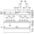
도 5 내지 도 7은 본 발명의 일 실시예에 따른 액정 표시 장치 리페어 방법을 도시한 단면도들이다.5 to 7 are sectional views illustrating a liquid crystal display repair method according to an embodiment of the present invention.
도면으로 도시하지 않았으나, 도 5에 앞서 도 4의 액정 표시 장치가 제조된다. 그 후 불량 화소 즉, 휘점 결함 또는 암점 결함을 갖는 화소의 유무를 판별하기 위한 검사 공정이 수행된다. 상기 검사 공정은 예를 들어 액정 표시 장치에 테스트 패턴을 구현하여 휘점 또는 암점의 유무 및 위치를 파악하는 방법으로 수행될 수 있다. 본 실시예에서는 백색을 표시하는 제2 화소 영역(10W)에 휘점 결함이 발생한 경우를 예로 하여 설명한다.Although not shown in the drawings, the liquid crystal display device of Fig. 4 is manufactured before Fig. Thereafter, an inspection process is performed to determine the presence or absence of a defective pixel, that is, a pixel having a bright spot defect or a dark dot defect. The inspection process may be performed by, for example, implementing a test pattern on a liquid crystal display device to determine the presence or absence of a luminescent spot or a dark spot. In the present embodiment, a case where a luminescent spot defect occurs in the
도 5를 참조하면, 제2 화소 영역(도면상 우측 개구 영역)에 레이저(400)를 조사하여, 제2 화소 영역 내 제2 베이스 기판(201)과 인접한 오버코트층(230) 에 미세 공동(micro cavity)을 형성한다. 미세 공동(500)은 상기 제2 화소 영역과 중첩하는 평면상 면적을 가지고 형성될 수 있다. 오버코트층(230)을 이루는 물질은 레이저(400)에 의해 융제(ablation)되며, 그 결과 제2 베이스 기판(201)과 오버코트층(230) 사이에 위치하는 미세 공동(500)을 형성할 수 있다. 미세 공동(500)의 두께는 차광 부재(210)의 두께와 같거나 작을 수 있으나 이에 제한되는 것은 아니다.5, a
전술한 바와 같이, 오버코트층(230)이 200 내지 400 nm의 자외선을 흡수할 수 있는 물질을 포함하기 때문에 레이저(400)에서 조사된 자외선이 오버코트층(230)을 투과하지 않고, 제2 베이스 기판(201)과 맞닿는 오버코트층(230)의 상부 계면에서 직접적으로 흡수가 일어날 수 있다. 오버코트층(230)이 자외선을 흡수하면 열 에너지가 발생하고, 오버코트층(230)을 구성하는 유기물 분자 간의 결합이 끊어지면서 중성원자, 분자, 양이온, 음이온을 포함하는 플라즈마를 포함하여 라디컬, 클러스터, 전자 및 양자를 방출하면서 융제가 일어날 수 있다.As described above, since the
이 경우 사용되는 레이저(400)의 파장은 오버코트층(230)이 이를 흡수할 수 있도록 200 내지 400 nm의 자외선 파장을 가질 수 있다. 레이저의 파장이 200 nm 이상이면 레이저에 의한 제2 베이스 기판(201)의 실질적인 손상 없이 레이저가 제2 베이스 기판을 투과할 수 있고, 레이저의 파장이 400 nm 이하이면 레이저가 오버코트층(230)을 투과하여 하부의 제2 배향막(280), 액정층(300) 또는 제1 기판 내의 전극이나 유기/무기막을 손상하는 것을 방지할 수 있다. In this case, the wavelength of the
또, 사용되는 레이저(400)는 450 내지 500 pico second(ps)의 펄스폭(pulse width)을 가질 수 있다. 펄스폭이 450 ps 이상이면 오버코트층(230)이 탄화(carbonization)되는 것을 방지할 수 있고, 펄스폭이 550 ps 이하이면 미세 공동을 효과적으로 형성할 수 있다.Also, the
제2 화소 영역에 조사되는 레이저(400)는 스캔 방식으로 조사될 수 있다. 즉, 소정의 유효 조사 면적(beam size)을 갖는 레이저(400)를 이동하면서 제2 화소 영역 전체 면적에 조사할 수 있다. 다만, 이에 제한되는 것은 아니며, 제2 화소 영역 전체 면적에 대응하는 조사 면적을 갖는 레이저를 한번에 조사하는 블록샷 방식으로 조사될 수도 있다.The
오버코트층(230)이 레이저(400)를 직접적으로 흡수하도록 함으로써, 오버코트층(230)이 제2 베이스 기판(201)과 맞닿는 상부 계면에서 레이저(400) 에너지 흡수가 직접적으로 발생하고, 제2 베이스 기판(201)과 오버코트층(230) 사이에 미세 공동(500)이 형성되기 때문에 오버코트층(230)이 융제되어 생성되는 이물 등이 액정층(300)을 오염하는 것을 미연에 방지할 수 있다. 또, 미세 공동(500)이 화소 전극(170b)이나 공통 전극(150)이 배치되지 않은 제2 기판(200) 내에 위치하기 때문에 전극의 대전 전하에 의한 이물의 영향을 최소화하고, 액정 표시 장치의 구동시 발생할 수 있는 잔상과 같은 불량을 방지할 수 있다.The absorption of the
또, 200 내지 400 nm의 자외선 파장을 갖는 레이저(400)를 이용하여 오버코트층(230) 내에 미세 공동(500)을 형성함으로써 후속 공정에서 사용되는 레이저와 동일한 레이저를 사용할 수 있고, 이를 통해 암점화 설비를 단일화 하여 공정성을 개선할 수 있는 효과가 있다.In addition, by forming the
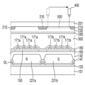
이어서 도 6을 참조하면, 제2 화소 영역(도면상 우측 개구 영역)과 인접한 적어도 하나의 차광 부재(210)에 레이저(400)를 조사하여 차광 부재(210)를 가공한다. 레이저(400)에 의해 조사된 차광 부재(210)는 차광 부재(210)를 구성하는 분자들 간의 결합이 끊어지면서 차광 부재 입자(210')들을 생성한다. 차광 부재 입자(210')들은 차광 부재(210)가 레이저(400)에 의해 열 에너지를 흡수하여 생성된 것일 수 있다. 차광 부재 입자(210')들은 소정의 유동성을 가질 수 있다. 차광 부재 입자(210'')들이 용출된 차광 부재(210)의 밀도는 차광 부재 입자들이 용출되기 전과 비교하여 더 작아질 수 있다. 몇몇 실시예에서는 차광 부재 입자들이 용출된 차광 부재의 두께는 차광 부재 입자들이 용출되기 전과 비교하여 더 얇아질 수도 있다.6, the
이 경우 사용되는 레이저(400)의 파장과 펄스폭은 미세 공동 형성시 사용한 레이저와 동일할 수 있다. 따라서, 전술한 바와 같이 동일한 레이저 장비를 이용하여 미세 공동(500)을 형성하고, 차광 부재(210)를 가공하기 때문에 설비의 교체를 생략할 수 있고 공정이 일체화되어 공정성을 개선할 수 있다.In this case, the wavelength and the pulse width of the
차광 부재(210)에 조사되는 레이저(400)는 스캔 방식으로 조사될 수 있다. 불량 화소 영역인 제2 화소 영역에 인접한 차광 부재의 가장자리를 따라 레이저(400)를 이동시키면서 차광 부재(210)를 가공할 수 있으나 이에 제한되는 것은 아니다.The
이어서, 레이저(400)를 차광 부재(210)로부터 제2 화소 영역(10W) 방향으로 스캔하는 방식으로 조사하여 차광 부재 입자(210')들을 확산시킨다. 유동성을 갖는 차광 부재 입자(210')들은 레이저(400)가 갖는 에너지를 흡수하여 연속적인 확산이 발생할 수 있으며, 레이저(400)의 이동 방향에 따라 차광 부재 입자(210')들의 확산 방향이 결정될 수 있다.Then, the
도 6은 제2 화소 영역의 좌측 차광 부재와 우측 차광 부재 각각으로부터 미세 공동(500) 중앙부 방향으로 레이저(400)를 조사하는 경우를 예시하고 있으나, 도시된 바와 달리 일측 차광 부재로부터 타측 차광 부재 방향으로 한번의 경로를 통해 레이저를 조사할 수도 있다.6 illustrates the case of irradiating the
제2 화소 영역의 좌측 차광 부재와 우측 차광 부재 각각으로부터 미세 공동(500) 중앙부 방향으로 레이저(400)를 조사하는 경우 차광 부재 입자(210')들 역시 차광 부재(210)로부터 누출되어, 평면상 제2 화소 영역 중앙부 방향으로 확산될 수 있다.When the
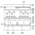
이어서 도 7을 참조하면, 제2 화소 영역(도면상 우측 영역)에 차광 부재의 면적이 확장된 암점화 부재(210'')가 형성된다. 암점화 부재(210'')는 데이터 라인과 중첩하는 차광 부재(미도시) 및 차광 부재 입자가 경화 또는 반경화되어 형성되며 개구 영역과 중첩하는 차광 부재(미도시)를 포함한다. 즉, 암점화 부재(210'')는 차광 부재(210)가 가공되어 생성된 차광 부재 입자(210')에 의해 차광 부재의 면적이 확장되어 형성되며, 차광 부재(210)와 상기 차광 부재 입자(210')가 경화 또는 반경화 되어 형성된 차광 부재는 물리적 경계가 시인되지 않을 수 있다. 도 7은 암점화 부재(210'')가 제2 화소 영역과 완전히 중첩하는 경우를 예시하고 있으나, 도시된 바와 달리 암점화 부재는 제2 화소 영역의 일부만을 중첩할 수도 있다. 또, 암점화 부재(210'')의 두께는 미세 공동의 두께와 실질적으로 동일할 수 있으며, 인접한 차광 부재(210)의 두께보다 작을 수 있으나, 이에 제한되지 않고 실질적으로 동일한 두께를 가질 수도 있다.7, a dark ignition member 210 '' having an expanded area of the light shielding member is formed in the second pixel region (the right side region in the drawing). The arm ignition member 210 '' includes a light shielding member (not shown) overlapping the data line and a light shielding member (not shown) formed by curing or semi-curing the shielding member particles and overlapping the opening region. That is, the arm ignition member 210 '' is formed by expanding the area of the light shielding member 210 'by the light shielding member particles 210' produced by processing the
암점화 부재(210'')가 점 결함을 갖는 불량 화소인 제2 화소 영역과 중첩함으로써 상기 제2 화소 영역을 투과하는 광을 실질적으로 차단시킬 수 있다. 따라서, 백색을 표시하던 제2 화소 영역은 화소 전극(170b)과 공통 전극(150)으로의 전압 인가 여부에 무관하게 항상 흑색을 표시하며, 이를 통해 제2 화소 영역의 암점화를 달성할 수 있다.It is possible to substantially block the light passing through the second pixel region by overlapping the second pixel region which is the defective pixel having the point defect, that is, the
이하, 본 발명의 다른 실시예들에 따른 액정 표시 장치 및 액정 표시 장치 리페어 방법을 설명한다. 다만, 발명의 본질을 흐리지 않기 위해 일 실시예에 따른 액정 표시 장치 및 일 실시예에 따른 액정 표시 장치 리페어 방법과 실질적으로 동일하거나 유사한 구성에 대한 설명은 생략하며, 이는 본 기술 분야의 통상의 기술자에게 명확히 이해될 수 있을 것이다.Hereinafter, a liquid crystal display and a liquid crystal display repairing method according to other embodiments of the present invention will be described. However, in order not to obscure the essence of the present invention, a description of a substantially same or similar configuration to the liquid crystal display device according to the embodiment and the liquid crystal display device repairing method according to the embodiment will be omitted, As will be clear to those skilled in the art.
도 8은 본 발명의 다른 실시예에 따른 액정 표시 장치의 단면도이다. 도 9 내지 도 11은 본 발명의 다른 실시예에 따른 액정 표시 장치 리페어 방법을 도시한 단면도들이다.8 is a cross-sectional view of a liquid crystal display device according to another embodiment of the present invention. 9 to 11 are cross-sectional views illustrating a liquid crystal display repair method according to another embodiment of the present invention.
도 8을 참조하면, 본 발명의 다른 실시예에 따른 액정 표시 장치의 제1 기판은 제1 베이스 기판(101), 복수의 박막 트랜지스터(미도시), 복수의 컬러 필터(221a, 221b), 공통 전극(150), 제1 화소 전극, 제2 화소 전극, 제1 배향막(180) 및 복수의 보호막/절연막 등을 포함할 수 있다.8, a first substrate of a liquid crystal display according to another embodiment of the present invention includes a
본 실시예에 따른 액정 표시 장치는 복수의 컬러 필터(221a, 221b)가 제2 기판이 아닌 제1 기판의 박막 트랜지스터 상에 배치되어 컬러 필터 온 어레이(color filter on array) 구조인 점이 도 4의 실시예에 따른 액정 표시 장치와 상이한 점이다.The liquid crystal display according to the present embodiment is different from the liquid crystal display according to the first embodiment in that a plurality of
구체적으로, 컬러 필터(221a, 221b)는 제1 기판의 보호막(141)과 제1 절연층(142) 사이에 배치된다. 컬러 필터(221a, 221b)는 보호막(141) 상에 배치되며 이웃하는 두 개의 데이터 라인들 사이에 배치되어 각 화소 영역(11R, 11G)들과 중첩할 수 있다.Specifically, the
예를 들어, 제1 화소 영역(11R)에는 적색의 컬러 필터(221a)가 배치될 수 있다. 액정 표시 패널 하부에 위치한 백라이트 유닛(미도시)으로부터 입사된 백색 광은 청색의 컬러 필터를 투과하여 적색 광만이 선택적으로 출사될 수 있다. 이를 통해 제1 화소 영역(11R)은 적색을 표시하는 화소 영역으로 시인될 수 있다. 또한, 제2 화소 영역(11G)에는 녹색의 컬러 필터(221b)가 배치될 수 있다. 백라이트 유닛으로부터 입사된 백색의 광은 적색의 컬러 필터를 투과하여 녹색 광만이 선택적으로 출사될 수 있다. 이를 통해 제2 화소 영역(11G)은 녹색을 표시하는 화소 영역으로 시인될 수 있다.For example, a
보호막(141) 및 복수의 컬러 필터(221a, 221b) 들 상에는 전면에 걸쳐 제1 절연층(142)이 배치된다. 제1 절연층(142)은 제1 베이스 기판(101) 상에 적층된 복수의 구성 요소의 높이를 균일하게 만들 수 있다.A first insulating
이어서, 제2 기판에 대해 설명한다. 제2 기판은 제2 베이스 기판(201), 차광 부재(211), 오버코트층(231) 및 제2 배향막(280) 등을 포함할 수 있다.Next, the second substrate will be described. The second substrate may include a
차광 부재(211)는 복수의 화소 영역 간의 경계 영역, 즉 데이터 라인들과 중첩하는 영역 및 박막 트랜지스터와 중첩하는 영역에 배치될 수 있다. 즉, 차광 부재(211)에 의해 복수의 화소 영역(11R, 11G)이 구획될 수 있다.The
차광 부재(211) 상에는 제2 베이스 기판(201) 전면에 걸쳐 오버코트층(231)이 배치된다. 오버코트층(231)은 200 내지 400 nm의 자외선을 흡수할 수 있는 물질을 포함한다. 본 실시예에 따른 오버코트층(231)은 전술한 도 4의 실시예에 따른 오버코트층(230)과 실질적으로 동일한 물질을 포함하여 이루어질 수 있는 바, 구체적인 설명은 생략한다.An
이하, 본 발명의 다른 실시예에 따른 액정 표시 장치 리페어 방법에 대해 설명한다. 본 실시예에서는 녹색을 표시하는 제2 화소 영역(11G)에 휘점 결함이 발생한 경우를 예로 하여 설명한다.Hereinafter, a liquid crystal display repair method according to another embodiment of the present invention will be described. In the present embodiment, a case where a luminescent spot defect occurs in the
도 9를 참조하면, 제2 화소 영역(도면상 우측 개구 영역)에 레이저(400)를 조사하여, 제2 화소 영역(11G) 내 제2 베이스 기판(201)과 인접한 오버코트층(231)에 미세 공동(501)을 형성한다. 오버코트층(231)을 이루는 물질은 레이저(400)에 의해 융제되며, 그 결과 제2 베이스 기판(201)과 오버코트층(231) 사이에 위치하는 미세 공동(501)을 형성할 수 있다. 이 경우 사용되는 레이저(400)의 파장은 오버코트층(231)이 이를 흡수할 수 있도록 200 내지 400 nm의 자외선 파장을 가짐은 전술한 바와 같다. 9, a
본 실시예의 경우 복수의 컬러 필터(221a, 221b)가 제2 기판이 아닌 제1 기판에 배치됨으로써 화소 영역(11R, 11G) 내에서 오버코트층(231)은 컬러 필터(221a, 221b)보다 상층에 위치한다. 따라서 제2 화소 영역(11G)에 레이저(400)가 조사되더라도, 오버코트층(231)이 레이저(400)를 우선적으로 흡수하기 때문에 제1 기판의 녹색의 컬러 필터(221b)에는 레이저(400)가 도달하지 않을 수 있다. 이를 통해 컬러 필터(221a, 221b)가 배치된 화소 영역과 중첩하는 오버코트층(231)에 미세 공동(501)을 형성할 수 있다.The plurality of
이어서 도 10을 참조하면, 제2 화소 영역(도면상 우측 개구 영역)과 인접한 적어도 하나의 차광 부재(211)에 레이저(400)를 조사하여 차광 부재(211)를 가공한다. 레이저(400)에 의해 조사된 차광 부재(211)는 차광 부재 입자(211')들을 생성한다.10, the
그 후, 레이저(400)를 차광 부재(211)로부터 제2 화소 영역(11G) 방향으로 스캔하는 방식으로 조사하여 차광 부재 입자(211')들을 확산시킨다. 제2 화소 영역의 좌측 차광 부재와 우측 차광 부재 각각으로부터 미세 공동(501) 중앙부 방향으로 레이저(400)를 조사하는 경우 차광 부재 입자(211')들 역시 차광 부재(211)로부터 누출되어, 평면상 제2 화소 영역 중앙부 방향으로 확산될 수 있다.Thereafter, the
이어서 도 11을 참조하면, 제2 화소 영역(도면상 우측 영역)에 차광 부재의 면적이 확장된 암점화 부재(211'')가 형성된다. 암점화 부재(211'')는 데이터 라인과 중첩하는 차광 부재(미도시) 및 차광 부재 입자가 경화 또는 반경화되어 형성되며 개구 영역과 중첩하는 차광 부재(미도시)를 포함한다. 암점화 부재(211'')가 제2 화소 영역과 중첩함으로써 상기 제2 화소 영역을 투과하는 광을 실질적으로 차단시킬 수 있다. 따라서, 녹색을 표시하던 제2 화소 영역(11G)은 화소 전극(170b)과 공통 전극(150)으로의 전압 인가 여부에 무관하게 항상 흑색을 표시하며, 이를 통해 제2 화소 영역의 암점화를 달성할 수 있다.11, a dark firing member 211 '' having an expanded area of the light shielding member is formed in the second pixel region (right side region in the drawing). The arm ignition member 211 '' includes a shielding member (not shown) that overlaps the data line and a shielding member (not shown) that is formed by curing or semi-curing the shielding member particles and overlaps the aperture region. The arm firing member 211 '' overlaps the second pixel region, thereby substantially blocking the light passing through the second pixel region. Accordingly, the
본 실시예의 경우, 컬러 필터가 배치된 화소 영역을 암점화하되, 컬러 필터에 어떠한 물리/화학적인 손상 없이 암점화 부재(211'')를 형성할 수 있다. 따라서 컬러 필터가 레이저를 흡수하여 생성될 수 있는 이물 등이 복수의 절연막 층간 사이에 부착되거나, 전계에 영향을 미치는 불량을 미연에 방지할 수 있으며, 필요에 따라 암점화 부재를 제거하여 화소 영역을 원복할 수도 있다.In the case of this embodiment, it is possible to form the
또한, 컬러 필터 내에 미세 공동을 형성할 경우, 컬러 필터 내에 포함된 안료(pigment)의 색에 따라 상이한 파장을 갖는 레이저를 조사해야 함에 반해, 본 실시예의 경우 컬러 필터가 아닌 오버코트층(231)에 미세 공동을 형성하여 암점화 부재(211'')를 충진시키기 때문에 서로 다른 색을 표시하는 화소 영역들을 동일한 파장을 갖는 레이저를 이용하여 암점화시킬 수 있는 효과가 있다. 이를 통해 리페어 공정에 사용되는 레이저 설비를 단일화 시킬 수 있다.In addition, in the case of forming the microcavities in the color filter, a laser having a different wavelength is required to be irradiated depending on the color of the pigment contained in the color filter. In contrast, in this embodiment, the laser light is irradiated onto the
이하, 본 발명의 또 다른 실시예에 따른 액정 표시 장치 및 액정 표시 장치 리페어 방법을 설명한다.Hereinafter, a liquid crystal display device and a liquid crystal display device repairing method according to another embodiment of the present invention will be described.
도 12는 본 발명의 또 다른 실시예에 따른 액정 표시 장치의 단면도이다. 도 13 내지 도 15는 본 발명의 또 다른 실시예에 따른 액정 표시 장치 리페어 방법을 도시한 단면도들이다.12 is a cross-sectional view of a liquid crystal display device according to another embodiment of the present invention. 13 to 15 are sectional views illustrating a liquid crystal display repair method according to another embodiment of the present invention.
도 12를 참조하면, 본 발명의 또 다른 실시예에 따른 액정 표시 장치의 제2 기판은 제2 베이스 기판(201), 차광 부재(212), 유기막층(232a), 컬러 필터(222), 오버코트층(232b) 및 제2 배향막(280) 등을 포함할 수 있다.12, a second substrate of a liquid crystal display according to another embodiment of the present invention includes a
본 실시예에 따른 액정 표시 장치는 컬러 필터(222)가 제2 베이스 기판(201) 상이 아닌 유기막층(232a) 상에 배치된 점이 도 4의 실시예에 따른 액정 표시 장치와 상이한 점이다.The liquid crystal display device according to this embodiment is different from the liquid crystal display device according to the embodiment shown in Fig. 4 in that the
차광 부재(212) 상에는 제2 베이스 기판(201) 전면에 걸쳐 유기막층(232a)이 배치된다. 유기막층(232a)은 차광 부재(212)가 들뜨는 것을 방지함과 동시에, 후술할 레이저 조사 공정을 통해 미세 공동이 형성될 수 있다. 유기막층(232a)은 200 내지 400 nm의 자외선을 흡수할 수 있는 물질을 포함한다. 본 실시예에 따른 유기막층(232a)은 전술한 도 4의 실시예에 따른 오버코트층(230)과 실질적으로 동일한 물질을 포함하여 이루어질 수 있는 바, 구체적인 설명은 생략한다.An
유기막층(232a) 상에는 화소 영역과 중첩하는 영역에 컬러 필터(222)가 배치될 수 있다. 구체적으로, 제1 화소 영역(12B)에는 청색의 컬러 필터(222)가 배치되어 청색을 표시하는 화소 영역으로 시인될 수 있다. 반면, 제2 화소 영역(12W)에는 컬러 필터가 배치되지 않고 백색을 표시하는 화소 영역으로 시인될 수 있다.A
유기막층(232a) 및 컬러 필터(222) 상에는 제2 베이스 기판(201) 전면에 걸쳐 오버코트층(232b)이 배치고, 오버코트층(232b) 상에는 제2 배향막(280)이 배치된다.An
이하, 본 발명의 또 다른 실시예에 따른 액정 표시 장치 리페어 방법에 대해 설명한다. 본 실시예에서는 청색을 표시하는 제1 화소 영역(11B)에 휘점 결함이 발생한 경우를 예로 하여 설명한다.Hereinafter, a liquid crystal display repairing method according to another embodiment of the present invention will be described. In this embodiment, a case where a luminescent spot defect occurs in the first pixel region 11B displaying blue is described as an example.
도 13을 참조하면, 제1 화소 영역(도면상 좌측 개구 영역)에 레이저(400)를 조사하여, 제1 화소 영역 내 제2 베이스 기판(201)과 인접한 유기막층(232a)에 미세 공동(502)을 형성한다. 유기막층(232a)을 이루는 물질은 레이저(400)에 의해 융제되며, 그 결과 제2 베이스 기판(201)과 유기막층(232a) 사이에 위치하는 미세 공동(502)을 형성할 수 있다. 이 경우 사용되는 레이저(400)의 파장은 유기막층(232a)이 이를 흡수할 수 있도록 200 내지 400 nm의 자외선 파장을 가짐은 전술한 바와 같다.13, a
본 실시예의 경우 컬러 필터(222)와 제2 베이스 기판(201) 사이에 유기막층(232a)이 위치함으로써 제1 화소 영역 내에서 유기막층(232a)은 컬러 필터(222)보다 상층에 위치한다. 따라서 제1 화소 영역에 레이저(400)가 조사되더라도, 유기막층(232a)이 레이저(400)를 우선적으로 흡수하기 때문에 컬러 필터(222)에는 레이저(400)가 도달하지 않을 수 있다. 이를 통해 제1 화소 영역과 중첩하는 유기막층(232a)에 미세 공동(502)을 형성할 수 있다.The
이어서 도 14를 참조하면, 제1 화소 영역(도면상 좌측 개구 영역)과 인접한 적어도 하나의 차광 부재(212)에 레이저(400)를 조사하여 차광 부재(212)를 가공한다. 레이저(400)에 의해 조사된 차광 부재(212)는 차광 부재 입자(212')들을 생성한다.14, the
그 후, 레이저(400)를 차광 부재(212)로부터 제1 화소 영역 방향으로 스캔하는 방식으로 조사하여 차광 부재 입자(212')들을 확산시킨다. 제1 화소 영역의 좌측 차광 부재와 우측 차광 부재 각각으로부터 미세 공동(502) 중앙부 방향으로 레이저(400)를 조사하는 경우 차광 부재 입자(212')들 역시 차광 부재(212)로부터 누출되어, 평면상 제1 화소 영역 중앙부 방향으로 확산될 수 있다.Thereafter, the
이어서 도 15를 참조하면, 제1 화소 영역(도면상 좌측 영역)에 차광 부재의 면적이 확장된 암점화 부재(212'')가 형성된다. 암점화 부재(212'')는 데이터 라인과 중첩하는 차광 부재(미도시) 및 차광 부재 입자가 경화 또는 반경화되어 형성되며 개구 영역과 중첩하는 차광 부재(미도시)를 포함한다. 암점화 부재(212'')가 제1 화소 영역과 중첩함으로써 상기 제1 화소 영역을 투과하는 광을 실질적으로 차단시킬 수 있다. 따라서, 청색을 표시하던 제1 화소 영역(12B)은 항상 흑색을 표시하며, 이를 통해 제1 화소 영역의 암점화를 달성할 수 있다.15, a dark firing member 212 '' having an expanded area of the light shielding member is formed in the first pixel region (left side region in the drawing). The arm ignition member 212 '' includes a shielding member (not shown) that overlaps the data line and a shielding member (not shown) that is formed by curing or semi-curing the shielding member particles and overlaps the opening region. The
본 실시예의 경우, 컬러 필터(222) 및 차광 부재(212)를 상부 기판인 제2 기판 상에 배치함으로써 공정을 단순화하고, 컬러 필터가 미세한 배선 및 패턴을 다수 포함하는 박막 트랜지스터 기판(제1 기판)에 형성될 경우 발생할 수 있는 불량을 방지하여 생성 수율을 높게 유지할 수 있다.In the present embodiment, the process is simplified by disposing the
또한, 컬러 필터에 어떠한 물리/화학적인 손상 없이 암점화 부재(212'')를 형성함으로써 컬러 필터가 분해되어 발생할 수 있는 이물 등에 의한 불량을 방지할 수 있으며, 서로 다른 색을 표시하는 화소 영역들을 동일한 파장을 갖는 레이저를 이용하여 암점화시킬 수 있는 효과가 있다.In addition, by forming the
도 16 내지 도 17은 본 발명의 또 다른 실시예들에 따른 액정 표시 장치의 단면도들이다.16 to 17 are sectional views of a liquid crystal display according to still another embodiment of the present invention.
도 16을 참조하면, 본 발명의 또 다른 실시예에 따른 액정 표시 장치는 제2 화소 영역(13W) 내 제2 베이스 기판(201)과 인접한 오버코트층(233)에 형성된 미세 공동(503)을 포함한다. 본 실시예의 미세 공동(503)은 제2 화소 영역(13W)의 일부만을 중첩하는 평면상 면적을 가질 수 있다.16, a liquid crystal display according to another embodiment of the present invention includes a
도 17을 참조하면, 본 발명의 또 다른 실시예에 따른 액정 표시 장치는 제2 화소 영역(14W)에 형성된 미세 공동 내에 차광 부재의 면적이 확장된 암점화 부재(214'')를 포함한다. 암점화 부재(214'')는 데이터 라인과 중첩하는 차광 부재(미도시) 및 차광 부재 입자가 경화 또는 반경화되어 형성되며 개구 영역과 중첩하는 차광 부재(미도시)를 포함한다. 본 실시예의 암점화 부재(214'')는 제2 화소 영역(14W)의 일부만을 중첩하는 평면상 면적을 가질 수 있다.Referring to FIG. 17, a liquid crystal display according to another embodiment of the present invention includes a dark firing member 214 '' having an area of a light shielding member expanded in a microcavity formed in a
액정 표시 장치의 특성상, 완전한 암점화가 요구되지 않는 경우 결함을 갖는 불량 화소 영역의 일부 영역에만 암점화 부재(214'')를 형성함으로써 실질적인 암점화를 달성함과 동시에 데이터 라인과 중첩하는 차광 부재의 가공을 최소화할 수 있다. When the complete dark pointing is not required, the
이상에서 본 발명의 실시예를 중심으로 설명하였으나 이는 단지 예시일 뿐 본 발명을 한정하는 것이 아니며, 본 발명이 속하는 분야에서 통상의 지식을 가진 자라면 본 발명의 실시예의 본질적인 특성을 벗어나지 않는 범위에서 이상에 예시되지 않은 여러 가지의 변형과 응용이 가능함을 알 수 있을 것이다. 예를 들어, 본 발명의 실시예에 구체적으로 나타난 각 구성 요소는 변형하여 실시할 수 있다. 그리고 이러한 변형과 응용에 관계된 차이점들은 첨부된 청구 범위에서 규정하는 본 발명의 범위에 포함되는 것으로 해석되어야 할 것이다.While the present invention has been described with reference to exemplary embodiments, it is to be understood that the invention is not limited to the disclosed exemplary embodiments, but many variations and modifications may be made without departing from the spirit and scope of the invention. It will be appreciated that many variations and applications not illustrated above are possible. For example, each component specifically shown in the embodiments of the present invention can be modified and implemented. It is to be understood that all changes and modifications that come within the meaning and range of equivalency of the claims are therefore intended to be embraced therein.
100 : 제1 기판
200 : 제2 기판
210 : 차광 부재
210' : 차광 부재 입자
210'' : 암점화 부재
220 : 컬러 필터
230 : 오버코트층
300 : 액정층100: first substrate
200: second substrate
210: Shading member
210 ': shielding member particles
210 ": arm ignition member
220: Color filter
230: Overcoat layer
300: liquid crystal layer
Claims (20)
상기 기판 상의 상기 오버코트층에 200 nm 내지 400 nm의 파장을 갖는 레이저를 조사하여 상기 기판과 상기 오버코트층 사이에 미세 공동을 형성하는 제1 레이저 조사 단계를 포함하는 액정 표시 장치 리페어 방법.Providing a liquid crystal display comprising a substrate, a light shielding member disposed on the substrate, and an overcoat layer disposed on the substrate and the light shielding member and containing a material absorbing a wavelength of 200 nm to 400 nm; And
And a first laser irradiating step of irradiating the overcoat layer on the substrate with a laser having a wavelength of 200 nm to 400 nm to form a microcavity between the substrate and the overcoat layer.
상기 제1 레이저 조사 단계 다음에,
상기 기판 상의 상기 차광 부재에 레이저를 조사하여 상기 차광 부재를 가공하는 제2 레이저 조사 단계를 더 포함하는 액정 표시 장치 리페어 방법.The method according to claim 1,
After the first laser irradiation step,
And a second laser irradiating step of irradiating the shielding member on the substrate with a laser to process the shielding member.
상기 제2 레이저 조사 단계 다음에,
상기 차광 부재가 가공되어 생성된 차광 부재 입자들을 상기 미세 공동 내로 확산시키는 제3 레이저 조사 단계를 더 포함하는 액정 표시 장치 리페어 방법.3. The method of claim 2,
After the second laser irradiation step,
And a third laser irradiating step of diffusing the light shielding member particles produced by processing the light shielding member into the microcavity.
상기 제3 레이저 조사 단계는,
상기 레이저를 상기 차광 부재로부터 상기 차광 부재와 인접한 상기 미세 공동 방향으로 스캔하는 방식으로 조사하는 액정 표시 장치 리페어 방법.The method of claim 3,
Wherein the third laser irradiation step comprises:
And irradiating the laser from the light shielding member in such a manner as to scan in the direction of the microcore adjacent to the light shielding member.
상기 레이저는 450 ps 내지 550 ps의 펄스폭(pulse width)을 갖는 액정 표시 장치 리페어 방법.The method according to claim 1,
Wherein the laser has a pulse width of 450 ps to 550 ps.
상기 200 nm 내지 400 nm의 자외선 파장을 흡수하는 물질은 컨쥬게이션 화합물, 알렌 계열 화합물, 알카인 계열 화합물, 티오에테르기를 포함하는 화합물, 카르보닐 계열 화합물, 에스테르기를 포함하는 화합물, 이민기를 포함하는 화합물, 아조 계열 화합물, 나이트로소기를 포함하는 화합물, 또는 케텐 계열 화합물 중 어느 하나 또는 하나 이상인 액정 표시 장치 리페어 방법.The method according to claim 1,
The material capable of absorbing the ultraviolet wavelength of 200 nm to 400 nm may be a conjugation compound, an allene-based compound, an alkane-based compound, a compound containing a thioether group, a carbonyl-based compound, a compound containing an ester group, , An azo-based compound, a compound containing a nitroso group, or a ketene-based compound.
상기 기판 상에 배치되어 제1 화소 영역 및 제2 화소 영역을 포함하는 복수의 화소 영역을 구획하는 제1 차광부;
상기 기판 상의 상기 제1 화소 영역에 배치되는 컬러 필터; 및
상기 기판, 상기 제1 차광부 및 상기 컬러 필터 상에 배치되되, 200 nm 내지 400 nm의 자외선 파장을 흡수하는 물질을 함유하는 오버코트층을 포함하는 액정 표시 장치.Board;
A first light-shielding portion disposed on the substrate and partitioning a plurality of pixel regions including a first pixel region and a second pixel region;
A color filter disposed in the first pixel region on the substrate; And
And an overcoat layer disposed on the substrate, the first light-shielding portion, and the color filter, the overcoat layer containing a material absorbing an ultraviolet wavelength of 200 nm to 400 nm.
상기 200 nm 내지 400 nm의 자외선 파장을 흡수하는 물질은 컨쥬게이션 화합물, 알렌 계열 화합물, 알카인 계열 화합물, 티오에테르기를 포함하는 화합물, 카르보닐 계열 화합물, 에스테르기를 포함하는 화합물, 이민기를 포함하는 화합물, 아조 계열 화합물, 나이트로소기를 포함하는 화합물, 또는 케텐 계열 화합물 중 어느 하나 또는 하나 이상인 액정 표시 장치.8. The method of claim 7,
The material capable of absorbing the ultraviolet wavelength of 200 nm to 400 nm may be a conjugation compound, an allene-based compound, an alkane-based compound, a compound containing a thioether group, a carbonyl-based compound, a compound containing an ester group, , An azo-based compound, a compound containing a nitroso group, or a ketene-based compound.
상기 200 nm 내지 400 nm의 자외선 파장을 흡수하는 물질은 상기 오버코트층을 구성하는 오버코트 조성물 내에서 0.001 wt% 이상 10.0 wt% 이하의 범위로 포함되는 액정 표시 장치.8. The method of claim 7,
Wherein the material capable of absorbing ultraviolet light having a wavelength of 200 nm to 400 nm is contained in an amount of 0.001 wt% or more and 10.0 wt% or less in the overcoat composition constituting the overcoat layer.
상기 제2 화소 영역의 적어도 일부와 중첩하는 영역에 형성되며,
상기 기판과 상기 오버코트층 사이에 형성된 미세 공동(micro cavity)을 더 포함하는 액정 표시 장치.8. The method of claim 7,
A second pixel region formed in a region overlapping at least a part of the second pixel region,
And a microcavity formed between the substrate and the overcoat layer.
상기 미세 공동 내에 형성되며, 인접한 상기 제1 차광부와 물리적 경계 없이 형성된 제2 차광부를 더 포함하는 액정 표시 장치.11. The method of claim 10,
And a second light-shielding portion formed in the microcavity and formed without a physical boundary with the adjacent first light-shielding portion.
상기 제1 기판 상에 배치되어 복수의 화소 영역을 구획하는 제1 차광부; 및
상기 제1 기판 및 상기 제1 차광부 상에 배치되되, 200 nm 내지 400 nm의 자외선 파장을 흡수하는 물질을 함유하는 유기막층을 포함하는 액정 표시 장치.A first substrate;
A first light-shielding portion disposed on the first substrate and partitioning a plurality of pixel regions; And
And an organic film layer disposed on the first substrate and the first light-shielding portion, the organic film layer containing a material absorbing an ultraviolet wavelength of 200 nm to 400 nm.
상기 유기막층 상에 배치되는 컬러 필터를 더 포함하는 액정 표시 장치.13. The method of claim 12,
And a color filter disposed on the organic film layer.
상기 컬러 필터의 적어도 일부와 중첩하는 영역에 형성되며,
상기 제1 기판과 상기 유기막층 사이에 형성된 미세 공동을 더 포함하는 액정 표시 장치.14. The method of claim 13,
The color filter being formed in an area overlapping at least a part of the color filter,
And a microcavity formed between the first substrate and the organic film layer.
상기 미세 공동 내에 형성되며, 인접한 제1 차광부와 물리적 경계 없이 형성된 제2 차광부를 더 포함하는 액정 표시 장치.15. The method of claim 14,
And a second light-shielding portion formed in the microcavity and formed without a physical boundary with the adjacent first light-shielding portion.
상기 제1 기판과 이격하여 대향하는 제2 기판; 및
상기 제2 기판 상에 배치되는 컬러 필터를 더 포함하는 액정 표시 장치.13. The method of claim 12,
A second substrate facing away from the first substrate; And
And a color filter disposed on the second substrate.
상기 컬러 필터의 적어도 일부와 중첩하는 영역에 형성되며,
상기 제1 기판과 상기 유기막층 사이에 형성된 미세 공동을 더 포함하는 액정 표시 장치.17. The method of claim 16,
The color filter being formed in an area overlapping at least a part of the color filter,
And a microcavity formed between the first substrate and the organic film layer.
상기 미세 공동 내에 형성되며, 인접한 제1 차광부와 물리적 경계 없이 형성된 제2 차광부를 더 포함하는 액정 표시 장치.18. The method of claim 17,
And a second light-shielding portion formed in the microcavity and formed without a physical boundary with the adjacent first light-shielding portion.
상기 200 nm 내지 400 nm의 자외선 파장을 흡수하는 물질은 컨쥬게이션 화합물, 알렌 계열 화합물, 알카인 계열 화합물, 티오에테르기를 포함하는 화합물, 카르보닐 계열 화합물, 에스테르기를 포함하는 화합물, 이민기를 포함하는 화합물, 아조 계열 화합물, 나이트로소기를 포함하는 화합물, 또는 케텐 계열 화합물 중 어느 하나 또는 하나 이상인 액정 표시 장치.13. The method of claim 12,
The material capable of absorbing the ultraviolet wavelength of 200 nm to 400 nm may be a conjugation compound, an allene-based compound, an alkane-based compound, a compound containing a thioether group, a carbonyl-based compound, a compound containing an ester group, , An azo-based compound, a compound containing a nitroso group, or a ketene-based compound.
상기 200 nm 내지 400 nm의 자외선 파장을 흡수하는 물질은 상기 유기막층을 구성하는 유기막 조성물 내에서 0.001 wt% 이상 10.0 wt% 이하의 범위로 포함되는 액정 표시 장치.13. The method of claim 12,
Wherein the material capable of absorbing ultraviolet light having a wavelength of 200 nm to 400 nm is contained in an organic film composition constituting the organic film layer in a range of 0.001 wt% to 10.0 wt%.
Priority Applications (2)
| Application Number | Priority Date | Filing Date | Title |
|---|---|---|---|
| KR1020150136426A KR102499179B1 (en) | 2015-09-25 | 2015-09-25 | Liquid crystal display device and reparing method thereof |
| US14/993,179 US10809550B2 (en) | 2015-09-25 | 2016-01-12 | Liquid crystal display device including first and second light blocking units |
Applications Claiming Priority (1)
| Application Number | Priority Date | Filing Date | Title |
|---|---|---|---|
| KR1020150136426A KR102499179B1 (en) | 2015-09-25 | 2015-09-25 | Liquid crystal display device and reparing method thereof |
Publications (2)
| Publication Number | Publication Date |
|---|---|
| KR20170037726A true KR20170037726A (en) | 2017-04-05 |
| KR102499179B1 KR102499179B1 (en) | 2023-02-10 |
Family
ID=58408925
Family Applications (1)
| Application Number | Title | Priority Date | Filing Date |
|---|---|---|---|
| KR1020150136426A Active KR102499179B1 (en) | 2015-09-25 | 2015-09-25 | Liquid crystal display device and reparing method thereof |
Country Status (2)
| Country | Link |
|---|---|
| US (1) | US10809550B2 (en) |
| KR (1) | KR102499179B1 (en) |
Cited By (1)
| Publication number | Priority date | Publication date | Assignee | Title |
|---|---|---|---|---|
| EP3650926A4 (en) * | 2017-07-07 | 2021-03-17 | BOE Technology Group Co., Ltd. | DISPLAY PANEL AND DISPLAY PANEL REPAIR PROCEDURE |
Families Citing this family (6)
| Publication number | Priority date | Publication date | Assignee | Title |
|---|---|---|---|---|
| US10600213B2 (en) * | 2016-02-27 | 2020-03-24 | Focal Sharp, Inc. | Method and apparatus for color-preserving spectrum reshape |
| CN107584819B (en) * | 2017-08-29 | 2019-10-15 | 京东方科技集团股份有限公司 | A touch substrate, its manufacturing method, and a touch device |
| TWI692744B (en) * | 2019-01-25 | 2020-05-01 | 友達光電股份有限公司 | Display panel |
| KR20220041286A (en) * | 2020-09-24 | 2022-04-01 | 삼성디스플레이 주식회사 | display panel and electric apparatus |
| CN112230459B (en) * | 2020-10-21 | 2024-05-10 | 苏州科韵激光科技有限公司 | Display panel bright point defect repairing system and repairing method |
| KR20220125104A (en) * | 2021-03-04 | 2022-09-14 | 삼성전자주식회사 | Display panel and electronic device including same |
Citations (2)
| Publication number | Priority date | Publication date | Assignee | Title |
|---|---|---|---|---|
| KR20070010876A (en) * | 2005-07-20 | 2007-01-24 | (주)미래컴퍼니 | Device and method for correcting faults of panel |
| KR20080111385A (en) * | 2007-06-18 | 2008-12-23 | 주식회사 코윈디에스티 | How to repair the bright point of display device |
Family Cites Families (10)
| Publication number | Priority date | Publication date | Assignee | Title |
|---|---|---|---|---|
| KR100778838B1 (en) * | 2000-12-30 | 2007-11-22 | 엘지.필립스 엘시디 주식회사 | LCD and its manufacturing method |
| KR101299646B1 (en) * | 2006-10-12 | 2013-08-26 | 삼성디스플레이 주식회사 | Display panel and method of manufacturing the same |
| KR101458913B1 (en) * | 2008-08-05 | 2014-11-07 | 삼성디스플레이 주식회사 | Liquid crystal display |
| TWI400540B (en) * | 2009-09-11 | 2013-07-01 | Hannstar Display Corp | Pixel structure of liquid crystal displaying panel |
| JP5550357B2 (en) | 2010-01-15 | 2014-07-16 | 株式会社ジャパンディスプレイ | Display device with front window |
| US8865274B2 (en) * | 2010-04-02 | 2014-10-21 | Samsung Display Co., Ltd. | Liquid crystal display device, alignment film, and methods for manufacturing the same |
| JP5285729B2 (en) * | 2011-03-03 | 2013-09-11 | 株式会社ジャパンディスプレイ | Liquid crystal display |
| JP5739217B2 (en) | 2011-04-22 | 2015-06-24 | 株式会社ジャパンディスプレイ | Liquid crystal display |
| KR101992884B1 (en) | 2011-12-21 | 2019-06-26 | 엘지디스플레이 주식회사 | Liquid crystal display device and method of fabricating the same |
| JP6147148B2 (en) * | 2013-09-03 | 2017-06-14 | 株式会社ジャパンディスプレイ | Alignment film material and liquid crystal display device using the same |
-
2015
- 2015-09-25 KR KR1020150136426A patent/KR102499179B1/en active Active
-
2016
- 2016-01-12 US US14/993,179 patent/US10809550B2/en active Active
Patent Citations (2)
| Publication number | Priority date | Publication date | Assignee | Title |
|---|---|---|---|---|
| KR20070010876A (en) * | 2005-07-20 | 2007-01-24 | (주)미래컴퍼니 | Device and method for correcting faults of panel |
| KR20080111385A (en) * | 2007-06-18 | 2008-12-23 | 주식회사 코윈디에스티 | How to repair the bright point of display device |
Cited By (2)
| Publication number | Priority date | Publication date | Assignee | Title |
|---|---|---|---|---|
| EP3650926A4 (en) * | 2017-07-07 | 2021-03-17 | BOE Technology Group Co., Ltd. | DISPLAY PANEL AND DISPLAY PANEL REPAIR PROCEDURE |
| US11237415B2 (en) | 2017-07-07 | 2022-02-01 | Boe Technology Group Co., Ltd. | Method for repairing a display panel and a display panel |
Also Published As
| Publication number | Publication date |
|---|---|
| US20170090223A1 (en) | 2017-03-30 |
| KR102499179B1 (en) | 2023-02-10 |
| US10809550B2 (en) | 2020-10-20 |
Similar Documents
| Publication | Publication Date | Title |
|---|---|---|
| KR20170037726A (en) | Liquid crystal display device and reparing method thereof | |
| US7733431B2 (en) | Laser repair structure and method for TFT-LCD | |
| US8673104B2 (en) | Fabricating method of liquid crystal display device | |
| US20080220553A1 (en) | Method of producing liquid crystal display device including forming an align mark in an insulating mother substrate | |
| KR20080084034A (en) | Color filter and manufacturing method of liquid crystal display | |
| CN101600984B (en) | Liquid crystal display device and method for manufacturing the same | |
| KR101473842B1 (en) | How to repair defective cells in liquid crystal display panel | |
| CN101784944B (en) | Method for manufacturing liquid crystal display unit | |
| JP6714898B2 (en) | Color filter substrate and manufacturing method thereof | |
| WO2016095338A1 (en) | Dark spot repair method for copper-interconnect coa type liquid crystal panel and copper-interconnect coa type liquid crystal panel structure | |
| JP4354946B2 (en) | Liquid crystal display panel and repair method thereof | |
| US7932983B2 (en) | Method for adjusting amount of liquid crystal in an LCD device including reducing the thickness of a seal member to form a repair region by laser heating a metal pattern thereunder | |
| KR101013647B1 (en) | Channel part repair method and liquid crystal display device using the same | |
| KR100577301B1 (en) | LCD and its manufacturing method | |
| JP2009128552A (en) | Liquid crystal display device and method of manufacturing liquid crystal display device | |
| JP2016194624A (en) | Liquid crystal panel, liquid crystal display, and method of correcting defect in luminous point of the same | |
| CN108254946B (en) | Display device, method and apparatus for manufacturing the same | |
| CN107121795B (en) | Display device and its manufacturing method and manufacturing device | |
| JP4660011B2 (en) | Liquid crystal display device and manufacturing method thereof | |
| KR101227137B1 (en) | Repairing apparatus for liquid crystal display and repairing method using the same | |
| KR101152555B1 (en) | An apparatus and method of repairing a pattern | |
| TW201704819A (en) | Liquid crystal display panel and manufacturing method thereof | |
| US10656485B2 (en) | Display device and method for manufacturing the same | |
| WO2008156280A1 (en) | Method of repairing flat pannel display | |
| WO2008156284A1 (en) | Method of repairing flat pannel display |
Legal Events
| Date | Code | Title | Description |
|---|---|---|---|
| PA0109 | Patent application |
Patent event code: PA01091R01D Comment text: Patent Application Patent event date: 20150925 |
|
| PG1501 | Laying open of application | ||
| A201 | Request for examination | ||
| PA0201 | Request for examination |
Patent event code: PA02012R01D Patent event date: 20200903 Comment text: Request for Examination of Application Patent event code: PA02011R01I Patent event date: 20150925 Comment text: Patent Application |
|
| E902 | Notification of reason for refusal | ||
| PE0902 | Notice of grounds for rejection |
Comment text: Notification of reason for refusal Patent event date: 20220420 Patent event code: PE09021S01D |
|
| N231 | Notification of change of applicant | ||
| PN2301 | Change of applicant |
Patent event date: 20220713 Comment text: Notification of Change of Applicant Patent event code: PN23011R01D |
|
| E701 | Decision to grant or registration of patent right | ||
| PE0701 | Decision of registration |
Patent event code: PE07011S01D Comment text: Decision to Grant Registration Patent event date: 20221129 |
|
| GRNT | Written decision to grant | ||
| PR0701 | Registration of establishment |
Comment text: Registration of Establishment Patent event date: 20230208 Patent event code: PR07011E01D |
|
| PR1002 | Payment of registration fee |
Payment date: 20230208 End annual number: 3 Start annual number: 1 |
|
| PG1601 | Publication of registration |