KR20150092209A - Led lighting devices with quantum dot glass containment plates - Google Patents
Led lighting devices with quantum dot glass containment plates Download PDFInfo
- Publication number
- KR20150092209A KR20150092209A KR1020157017217A KR20157017217A KR20150092209A KR 20150092209 A KR20150092209 A KR 20150092209A KR 1020157017217 A KR1020157017217 A KR 1020157017217A KR 20157017217 A KR20157017217 A KR 20157017217A KR 20150092209 A KR20150092209 A KR 20150092209A
- Authority
- KR
- South Korea
- Prior art keywords
- quantum dot
- light source
- glass
- bulkhead plate
- color conversion
- Prior art date
Links
Images

Classifications
-
- H—ELECTRICITY
- H01—ELECTRIC ELEMENTS
- H01L—SEMICONDUCTOR DEVICES NOT COVERED BY CLASS H10
- H01L33/00—Semiconductor devices with at least one potential-jump barrier or surface barrier specially adapted for light emission; Processes or apparatus specially adapted for the manufacture or treatment thereof or of parts thereof; Details thereof
- H01L33/48—Semiconductor devices with at least one potential-jump barrier or surface barrier specially adapted for light emission; Processes or apparatus specially adapted for the manufacture or treatment thereof or of parts thereof; Details thereof characterised by the semiconductor body packages
- H01L33/50—Wavelength conversion elements
- H01L33/505—Wavelength conversion elements characterised by the shape, e.g. plate or foil
-
- H—ELECTRICITY
- H01—ELECTRIC ELEMENTS
- H01L—SEMICONDUCTOR DEVICES NOT COVERED BY CLASS H10
- H01L33/00—Semiconductor devices with at least one potential-jump barrier or surface barrier specially adapted for light emission; Processes or apparatus specially adapted for the manufacture or treatment thereof or of parts thereof; Details thereof
- H01L33/02—Semiconductor devices with at least one potential-jump barrier or surface barrier specially adapted for light emission; Processes or apparatus specially adapted for the manufacture or treatment thereof or of parts thereof; Details thereof characterised by the semiconductor bodies
- H01L33/04—Semiconductor devices with at least one potential-jump barrier or surface barrier specially adapted for light emission; Processes or apparatus specially adapted for the manufacture or treatment thereof or of parts thereof; Details thereof characterised by the semiconductor bodies with a quantum effect structure or superlattice, e.g. tunnel junction
-
- H—ELECTRICITY
- H01—ELECTRIC ELEMENTS
- H01L—SEMICONDUCTOR DEVICES NOT COVERED BY CLASS H10
- H01L33/00—Semiconductor devices with at least one potential-jump barrier or surface barrier specially adapted for light emission; Processes or apparatus specially adapted for the manufacture or treatment thereof or of parts thereof; Details thereof
- H01L33/48—Semiconductor devices with at least one potential-jump barrier or surface barrier specially adapted for light emission; Processes or apparatus specially adapted for the manufacture or treatment thereof or of parts thereof; Details thereof characterised by the semiconductor body packages
- H01L33/50—Wavelength conversion elements
- H01L33/501—Wavelength conversion elements characterised by the materials, e.g. binder
- H01L33/502—Wavelength conversion materials
- H01L33/504—Elements with two or more wavelength conversion materials
-
- H—ELECTRICITY
- H01—ELECTRIC ELEMENTS
- H01L—SEMICONDUCTOR DEVICES NOT COVERED BY CLASS H10
- H01L33/00—Semiconductor devices with at least one potential-jump barrier or surface barrier specially adapted for light emission; Processes or apparatus specially adapted for the manufacture or treatment thereof or of parts thereof; Details thereof
- H01L33/48—Semiconductor devices with at least one potential-jump barrier or surface barrier specially adapted for light emission; Processes or apparatus specially adapted for the manufacture or treatment thereof or of parts thereof; Details thereof characterised by the semiconductor body packages
- H01L33/52—Encapsulations
-
- H—ELECTRICITY
- H01—ELECTRIC ELEMENTS
- H01L—SEMICONDUCTOR DEVICES NOT COVERED BY CLASS H10
- H01L2224/00—Indexing scheme for arrangements for connecting or disconnecting semiconductor or solid-state bodies and methods related thereto as covered by H01L24/00
- H01L2224/01—Means for bonding being attached to, or being formed on, the surface to be connected, e.g. chip-to-package, die-attach, "first-level" interconnects; Manufacturing methods related thereto
- H01L2224/42—Wire connectors; Manufacturing methods related thereto
- H01L2224/47—Structure, shape, material or disposition of the wire connectors after the connecting process
- H01L2224/48—Structure, shape, material or disposition of the wire connectors after the connecting process of an individual wire connector
- H01L2224/4805—Shape
- H01L2224/4809—Loop shape
- H01L2224/48091—Arched
-
- H—ELECTRICITY
- H01—ELECTRIC ELEMENTS
- H01L—SEMICONDUCTOR DEVICES NOT COVERED BY CLASS H10
- H01L2924/00—Indexing scheme for arrangements or methods for connecting or disconnecting semiconductor or solid-state bodies as covered by H01L24/00
- H01L2924/10—Details of semiconductor or other solid state devices to be connected
- H01L2924/11—Device type
- H01L2924/12—Passive devices, e.g. 2 terminal devices
- H01L2924/1204—Optical Diode
- H01L2924/12041—LED
-
- H—ELECTRICITY
- H01—ELECTRIC ELEMENTS
- H01L—SEMICONDUCTOR DEVICES NOT COVERED BY CLASS H10
- H01L2924/00—Indexing scheme for arrangements or methods for connecting or disconnecting semiconductor or solid-state bodies as covered by H01L24/00
- H01L2924/15—Details of package parts other than the semiconductor or other solid state devices to be connected
- H01L2924/181—Encapsulation
Abstract
칩-온-보드(COB) 발광 다이오드(LED) 광원, 광원 캡슐화재, 양자점 분포 색 변환 매체, 및 양자점 유리 격벽 플레이트를 포함하는 발광 소자가 제공된다. 상기 COB LED 광원은 적어도 하나의 LED를 포함하고 상기 광원 캡슐화재가 상기 LED에 걸쳐 분포되는 광원 캡슐화재 공동을 규정한다. 상기 양자점 유리 격벽 플레이트는 상기 광원 캡슐화재 공동에 걸쳐 위치되고 상기 양자점 분포 색 변환 매체를 포함한다. 상기 양자점 분포 색 변환 매체는 양자점 구조를 포함하고 상기 양자점 유리 격벽 플레이트 내에 발광 소자의 방출 영역에 걸쳐 2차원으로 분포된다.There is provided a light emitting device comprising a chip-on-board (COB) light emitting diode (LED) light source, a light source capsule fire, a quantum dot distribution color conversion medium, and a quantum dot glass bulkhead plate. The COB LED light source includes at least one LED and defines a light source capsule fire cavity in which the light source capsule fire is distributed over the LED. The quantum dot glass bulkhead plate is positioned over the light source capsule fire cavity and comprises the quantum dot color conversion medium. The quantum dot color conversion medium includes a quantum dot structure and is two-dimensionally distributed over the emission region of the light emitting device in the quantum dot glass bulkhead plate.
Description
본 출원은 2012년 11월 30일 출원된 미국 가출원 제61/731,530호 및 2013년 3월 14일 출원된 미국 출원 제13/828,169호를 우선권 주장한다.This application claims priority to U.S. Provisional Application No. 61 / 731,530, filed November 30, 2012, and U.S. Application No. 13 / 828,169, filed March 14,
본 발명 개시는 발광 다이오드(LED) 발광 소자에 관한 것으로, 좀더 구체적으로 패키지된 칩-온-보드(COB; packaged chip-on-board) LED 어레이에 관한 것이다.The present disclosure relates to light emitting diode (LED) light emitting devices, and more particularly to packaged chip-on-board (COB) LED arrays.
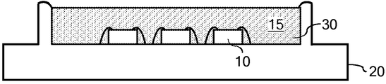
먼저 도 1과 관련하여, 고휘도 LED 발광 소자, 즉 1000 루멘(lumen)에 근접하거나 이를 초과하는 광원은 통상 예컨대 금속 피복 PC 보드(20)에 고정된 2차원 어레이로 구성된 많은 다수의 청색 LED(10)들을 필요로 한다. 많은 경우, 그러한 다이오드 어레이는 실리콘 캡슐화재(15; silicone encapsulant)로 분산된 색 변환 형광체(30)에 의해 덮여진다. 이들 및 다른 타입의 COB LED 어레이들은 형태, 광 출력, 및 전기적 구동 요건들이 표준화되어 있으며, 생각하건대 새로운 발광 표준이 될 수 있다.First, with reference to FIG. 1, a high brightness LED light emitting device, i.e., a light source close to or exceeding a lumen of 1000, typically comprises a large number of blue LEDs 10 ). In many cases, such a diode array is covered by a
본 발명은 양자점 유리 격벽 플레이트를 구비한 LED 발광 소자를 제공하기 위한 것이다.The present invention provides a LED light emitting device having a quantum dot glass bulkhead plate.
본 발명 개시의 목적에 따르면, 칩-온-보드(COB) 발광 다이오드(LED) 광원, 광원 캡슐화재, 양자점 분포 색 변환 매체, 및 양자점 유리 격벽 플레이트를 포함하는 발광 소자가 제공된다. 상기 COB LED 광원은 적어도 하나의 LED를 포함하고, 상기 광원 캡슐화재가 그 LED에 걸쳐 분포되는 광원 캡슐화재 공동(light source encapsulant cavity)을 규정한다. 상기 양자점 유리 격벽 플레이트는 상기 광원 캡슐화재 공동에 걸쳐 위치되고, 양자점 분포 색 변환 매체를 포함한다. 상기 양자점 분포 색 변환 매체는 양자점 구조를 포함하고, 상기 양자점 유리 격벽 플레이트 내에 발광 소자의 방출 영역에 걸쳐 2차원으로 분포된다.According to an aspect of the present disclosure, there is provided a light emitting device including a chip-on-board (COB) light emitting diode (LED) light source, a light source capsule fire, a quantum dot distribution color conversion medium, and a quantum dot glass bulkhead plate. The COB LED light source includes at least one LED and defines a light source encapsulant cavity in which the light source capsule fire is distributed over the LED. The quantum dot glass bulkhead plate is positioned over the light source capsule fire cavity and includes a quantum dot color conversion medium. The quantum dot color conversion medium includes a quantum dot structure, and is distributed two-dimensionally over the emission region of the light emitting element in the quantum dot glass bulkhead plate.
본 발명 개시의 양자점 유리 격벽 플레이트는 추가의 제조 공정 제어를 제공하기 때문에 이점이 있다. 구체적으로, 그러한 양자점 유리 격벽 플레이트는 대응하는 LED 어레이로부터 분리적으로 테스트될 수 있고, 적절한 플레이트-투-어레이 쌍(plate-to-array pairing)이 원하는 색 출력을 달성하도록 이루어질 수 있다. 이는, 비록 본 발명 개시의 실시예들이 변환 매체의 사용을 고려할 지라도, LED 어레이를 캡슐화하는데 사용된 실리콘의 슬러리가 그 실리콘의 슬러리로 제공됨에 따라 변환 매체가 제공된 때의 케이스는 아니다.The quantum dot glass bulkhead plate of the present disclosure is advantageous because it provides additional manufacturing process control. Specifically, such a quantum dot glass bulkhead plate can be tested separately from the corresponding LED array, and a suitable plate-to-array pairing can be made to achieve the desired color output. This is not the case when a conversion medium is provided as the slurry of silicon used to encapsulate the LED array is provided as a slurry of the silicon, even though embodiments of the present disclosure contemplate the use of conversion media.
색 변환 매체가 로딩된 유리 격벽 플레이트는 단지 LED 어레이의 와이어 본드(wire bond) 상에 위치한다. 열등한 열 전도체인 공기가 아닌 순수 실리콘이 LED 주위에 사용될 수 있다. 이는 LED 상에 실리콘의 두께가 와이어 본드의 높이로 감소될 수 있다는 것을 의미하는데, 즉 약 50㎛의 매우 낮은 프로파일의 다양한 와이어 본드의 높이로 감소될 수 있다는 것을 의미한다. 이러한 구조는 다방면에 이점이 있다. 우선 색 변환 매체 자체는 이 매체가 실리콘으로 분산되는 경우보다 높은 온도에 견딜 수 있다. 더욱이, 패키지된 LED의 히트 싱크(heat sink)에 대한 채널 히트의 능력은 LED 상의 실리콘 층의 두께가 약 750㎛에서 약 50㎛로 크게 감소되기 때문에 크게 향상된다. 더 한층 두께의 감소는 와이어 본드가 더 이상 두께 요건을 부추기지 않아 플립-칩 LED 어레이를 가능하게 할 수 있을 것이라 생각된다. 아마도 처음엔 반 직관적이지만, 양자점에 의해 생성된 열에 대한 열 방산 경로는 LED 자체에 존재한다. 양자점 유리 격벽 플레이트의 유리는 실리콘 및 LED로부터 양자점을 분리하는데, 그래서 열 전달 관점에서, 가능한 한 얇은 격벽 플레이트의 유리를 만드는 것이 바람직하다. 또한 주목할 만한 것은 양자점 유리 격벽 플레이트에 포함된 양자점 매체가 통상 양자점에서 LED 어레이까지 열 통로 길이를 더 감소시키는데, 즉 단지 두께가 약 100㎛ 정도만 필요하다는 것이다.The glass bulkhead plate loaded with the color conversion medium is simply located on the wire bond of the LED array. Pure silicon can be used around the LED, not the inferior thermal conductor, air. This means that the thickness of the silicon on the LED can be reduced to the height of the wire bond, i.e. it can be reduced to the height of various wire bonds of a very low profile of about 50 mu m. This structure has many advantages. The color conversion medium itself can withstand a higher temperature than when the medium is dispersed in silicon. Moreover, the ability of the channel hits to the heat sink of the packaged LED is greatly improved because the thickness of the silicon layer on the LED is greatly reduced from about 750 占 퐉 to about 50 占 퐉. Further reduction in thickness is believed to enable the wire bond to no longer lead to thickness requirements and enable flip-chip LED arrays. Perhaps intuitively at first, the heat dissipation path for the heat generated by the quantum dot is in the LED itself. The glass of the quantum dot glass bulkhead plate separates the quantum dots from the silicon and the LED, so from a heat transfer point of view, it is desirable to make the glass of the bulkhead plate as thin as possible. Also noteworthy is that the quantum dot media included in the quantum dot glass bulkhead plate typically reduces the thermal path length from the quantum dot to the LED array, i.e. only about 100 microns in thickness.
본 발명 개시의 일 실시예에 따르면, 양자점 유리 격벽 플레이트는 유리 프레임을 포함하고, 그러한 양자점 구조는 상기 유리 프레임의 내부 볼륨(interior volume) 내에 포함된다. 이러한 실시예의 몇몇 예들이 이하 좀더 상세히 기술되는 도 2-4에 나타나 있다.According to one embodiment of the present disclosure, the quantum dot glass bulkhead plate comprises a glass frame, and such quantum dot structure is contained within the interior volume of the glass frame. Some examples of such embodiments are shown in Figures 2-4, which are described in greater detail below.
본 발명 개시의 다른 실시예에 따르면, 광원 캡슐화재는 제1분포 색 변환 매체를 포함하고, 상기 양자점 유리 격벽 플레이트의 그러한 색 변환 매체는 발광 소자의 보조 방출 영역을 규정하며, 그러한 제1분포 색 변환 매체에 의해 규정된 방출 영역은 상기 양자점 유리 격벽 플레이트에 의해 규정된 보조 방출 영역과 공간적으로(spatially) 일치하나 스펙트럼적으로(spectrally) 다르다. 이러한 실시예의 일 예가 이하 좀더 상세히 기술하는 도 2에 나타나 있다.According to another embodiment of the present disclosure, the light source capsule fire comprises a first distributed color conversion medium, and such a color conversion medium of the quantum dot glass bulkhead plate defines an auxiliary emission area of the light emitting element, The emission region defined by the conversion medium is spatially coincident but spectrally different from the auxiliary emission region defined by the quantum dot glass bulkhead plate. One example of such an embodiment is shown in FIG. 2, which is described in more detail below.
본 발명 개시의 또 다른 실시예에 따르면, 발광 소자는 제1분포 형광체 색 변환 매체를 포함하는 제1유리 격벽 플레이트를 포함하고, 상기 양자점 유리 격벽 플레이트의 그러한 색 변환 매체는 발광 소자의 보조 방출 영역을 규정하며, 그러한 분포 형광체 색 변환 매체에 의해 규정된 방출 영역은 상기 양자점 유리 격벽 플레이트에 의해 규정된 보조 방출 영역과 공간적으로 일치하나 스펙트럼적으로 다르다. 이러한 실시예의 일 예가 이하 좀더 상세히 기술하는 도 3에 나타나 있다.According to another embodiment of the present disclosure, the light emitting device comprises a first glass bulkhead plate comprising a first distributed phosphor color conversion medium, and such color conversion media of the quantum dot glass bulkhead plate are arranged in the auxiliary emission region , And the emission region defined by such a distributed phosphor color conversion medium is spatially identical but spectrally different from the auxiliary emission region defined by the quantum dot glass bulkhead plate. One example of such an embodiment is shown in FIG. 3, which is described in more detail below.
본 발명 개시의 추가 실시예에 따르면, COB LED 광원은 열 히트 싱크 프레임워크(thermal heat sink framework)를 포함하고, 광원 캡슐화재는 소정의 분포 색 변환 매체에 자유로우며, 그러한 광원 캡슐화재는 실리콘을 포함하고, 양자점 유리 격벽 플레이트는 광원 캡슐화재 공동에 걸쳐 위치되며, 상기 광원 캡슐화재는 LED를 캡슐화 하기에 충분하고 상기 양자점 유리 격벽 플레이트의 분포 색 변환 매체로부터 열 히트 싱크 프레임워크로 상기 광원 캡슐화재를 통해 확장되는 캡슐화재 열전도로(TPE)를 규정하는 두께로 LED에 걸쳐 분포되며, 상기 광원 캡슐화재의 두께는 상기 열전도로(TPE)가 상기 광원 캡슐화재를 통해 약 100 ㎛ 미만으로 확장되는 두께이다. 이러한 실시예의 일 예가 이하 좀더 상세히 기술되는 도 4에 나타나 있다.According to a further embodiment of the disclosure of the present invention, the COB LED light source comprises a thermal heat sink framework, and the light source capsule fire is free of any distributed color conversion medium, And wherein the quantum dot glass bulkhead plate is positioned over the light source capsule fire cavity, wherein the light source capsule fire is sufficient to encapsulate the LED and the quantum dot glass bulkhead plate is distributed from the distribution color conversion medium of the quantum dot glass bulkhead plate to the heat sink framework the capsule fire thermal conduction extending through and distributed over the LED to have a thickness that defines a (T PE), thickness of the light source capsule fire is extended to less than about 100 ㎛ through the (T PE) as the heat conductive light source capsule fire Lt; / RTI > One example of such an embodiment is shown in FIG. 4, which is described in more detail below.
본 발명 개시의 특정 실시예들에 대한 이하의 상세한 설명은 다음의 도면들과 연계하여 참조하면 더 잘 이해될 수 있으며, 유사한 구조에는 유사한 참조부호가 표시된다:
도 1은 실리콘 색 변환 매체 내장 형광체를 채용하는 LED 발광 소자를 나타내고;
도 2는 본 발명 개시의 일 실시예에 따른 LED 발광 소자의 개략도이고;
도 3은 본 발명 개시의 다른 실시예에 따른 LED 발광 소자의 개략도이며;
도 4는 본 발명 개시의 또 다른 실시예에 따른 LED 발광 소자의 개략도이다.BRIEF DESCRIPTION OF THE DRAWINGS The following detailed description of specific embodiments of the present disclosure may be better understood when read in conjunction with the following drawings, wherein like structure is designated by like reference designations:
1 shows a LED light emitting element employing a phosphor having a built-in silicone color conversion medium;
2 is a schematic diagram of a LED light emitting device according to an embodiment of the disclosure of the present invention;
3 is a schematic view of an LED light emitting device according to another embodiment of the disclosure of the present invention;
4 is a schematic diagram of an LED light emitting device according to another embodiment of the present disclosure.
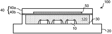
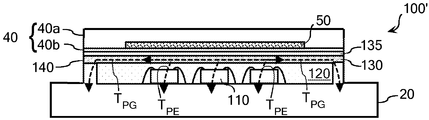
도 2-4는 적어도 하나의 LED(110), 광원 캡슐화재(120), 양자점 색 변환 매체(50), 양자점 유리 격벽 플레이트(40), 및 예컨대 금속 피복 인쇄회로기판(20) 형태의 열 히트 싱크 프레임워크를 포함하는 COB LED 발광 소자(100, 100', 100'')를 나타낸다. 상기 양자점 분포 색 변환 매체(50)는 상기 양자점 유리 격벽 플레이트(40) 내에 LED 발광 소자의 방출 영역(즉, 발광 영역)에 걸쳐 2차원으로 분포되고, LED의 방출(발광) 스펙트럼을 보다 길거나 또는 보다 짧은 파장으로 변환시키도록 구성된 양자점 구조를 포함한다.Figures 2-4 illustrate an embodiment of at least one
구체적으로 도 2-4의 구성에 따르면, 상기 양자점 유리 격벽 플레이트(40)는 상기 양자점 분포 색 변환 매체(50)를 수용하기 위한 대향의 밀봉 유리 패널(40a, 40b)들간 규정된 내부 볼륨을 포함하는 유리 격벽 프레임의 형태로 존재한다는 것을 알아야 한다. 그러한 대향의 밀봉 유리 패널들은 하나의 공동(cavity) 유리(40a) 및 하나의 밀봉(sealing) 유리(40b)를 포함한다. 상기 밀봉 유리(40b)는 통상 코닝사로부터 이용가능한 매우 얇은(통상 100 mm) 버전의 EAGLE XG® 디스플레이 유리인 Willow와 같은 비교적 얇은(약 100 ㎛) 디스플레이 등급 유리이다. 적절한 공동은 소정 기존의 또는 아직 개발되지 않은 유리 몰딩 또는 예컨대 미세 기계가공, 레이저-지원 기계가공 또는 밀링(milling), 레이저 절삭, 에칭, 또는 그 조합을 포함하는 유리 기계가공 기술에 의해 공동 유리(40a)에 제공될 수 있다. 다음에 스퍼터(sputter)된 유리가 밀봉 유리(40b)의 하면 상에 배치될 수 있고, 레이저는 양자점이 그 공동 내에 안착되는 동안 그러한 공동 유리에 상기 밀봉 유리(40b)를 둘레 결합시키는데 사용될 수 있다.Specifically, according to the configuration of FIG. 2-4, the quantum dot
한 세트의 고려된 실시예들에 따르면, 상술한 양자점을 포함하기 위한 밀봉 유리 패널은 밀봉 유리, 공동 유리 또는 그 모두의 밀봉면의 주변부를 따라 비교적 낮은 용융 온도(즉, 낮은 Tg) 유리 밀봉 스트립(sealing strip)을 제공함으로써 구성될 것이다. 이런 식으로, 상기 공동 유리 및 밀봉 유리는, 결합 구성을 생성할 때, 그러한 양자점을 포함하는 내부 볼륨을 규정하기 위해 유리 밀봉 스트립과 협조한다. 상기 유리 밀봉 스트립은 예컨대 스퍼터링 타겟으로부터 스퍼터링함으로써 물리적 증착에 의해 증착될 것이다.According to a set of contemplated embodiments, the sealed glass panel for containing the quantum dots described above has a relatively low melting temperature (i.e., low Tg) along the periphery of the sealing surface of the sealing glass, cavity glass, thereby providing a sealing strip. In this way, the cavity glass and the sealing glass cooperate with the glass sealing strip to define an internal volume that includes such quantum dots when creating a bonding configuration. The glass sealing strip will be deposited by physical vapor deposition, for example, by sputtering from a sputtering target.
초점 레이저 빔은 밀봉 인터페이스(sealed interface)를 형성하기 위해 낮은 용융 온도의 유리 밀봉 스트립 부근의 유리 기판 재료를 국부적으로 용융시키기 위해 사용될 수 있다. 한가지 접근방식에 있어서, 레이저는 공동 유리 또는 밀봉 유리를 통해 초점된 후 공동 유리 및 밀봉 유리의 인접한 부분 및 유리 밀봉 스트립을 국부적으로 가열하도록 위치적으로 스캔될 수 있다. 유리 밀봉 스트립의 국부 용융에 영향을 주기 위해, 유리 밀봉 스트립은 레이저 처리 파장에서 적어도 약 15%를 흡수하게 하는 것이 바람직하다. 상기 공동 유리 및 밀봉 유리는 통상 레이저 처리 파장에서 투명하다(예컨대, 적어도 50%, 70%, 80% 또는 90% 투명).The focus laser beam can be used to locally melt the glass substrate material near the glass sealing strip at low melting temperatures to form a sealed interface. In one approach, the laser can be focused locally through the cavity glass or the sealing glass and subsequently locally heated to the adjacent portions of the cavity glass and the sealing glass and the glass sealing strip. To effect local melting of the glass sealing strip, it is preferred that the glass sealing strip absorb at least about 15% at the laser processing wavelength. The cavity glass and the seal glass are typically transparent (e.g., at least 50%, 70%, 80%, or 90% transparent) at the laser processing wavelength.
다른 대안의 실시예에 있어서, 패턴된 유리 밀봉 스트립의 형성 대신, 밀봉(낮은 용융 온도) 유리의 블랭킷 층(blanket layer)이 밀봉 유리의 거의 모든 표면에 걸쳐 형성될 수 있다. 공동 유리/밀봉 유리 층/밀봉 유리를 포함하는 조립된 구조는 상기와 같이 조립될 수 있으며, 레이저는 두 기판간 밀봉 인터페이스를 국부적으로 규정하기 위해 사용될 수 있다.In another alternative embodiment, instead of forming a patterned glass sealing strip, a blanket layer of a sealed (low melting temperature) glass may be formed over substantially all of the surface of the sealing glass. The assembled structure including the cavity glass / seal glass layer / seal glass can be assembled as described above, and the laser can be used to locally define the seal interface between the two substrates.
레이저 500은 밀봉에 영향을 주기 위한 소정의 적절한 출력을 가질 수 있다. 일 예의 레이저로는 일반적인 디스플레이 유리에 대한 투명도 범위를 나타내는 355 nm 레이저와 같은 UV 레이저가 있다. 적절한 레이저 파워는 약 5 W 내지 약 6.15 W의 범위가 될 수 있다. 레이저의 이동 속도(밀봉율)는 약 1 mm/sec 내지 100 mm/sec의 범위가 될 수 있는데, 즉 1, 2, 5, 10, 20, 50 또는 100 mm/sec가 될 수 있다. 그러한 레이저 스폿(spot) 크기(직경)는 약 0.5 내지 1 mm가 될 수 있다.The laser 500 may have any suitable output to affect the seal. One example of a laser is a UV laser, such as a 355 nm laser, that represents the transparency range for a typical display glass. A suitable laser power may range from about 5 W to about 6.15 W. The moving speed (sealing rate) of the laser can be in the range of about 1 mm / sec to 100 mm / sec, i.e. 1, 2, 5, 10, 20, 50 or 100 mm / sec. Such a laser spot size (diameter) may be about 0.5 to 1 mm.
그러한 레이저 스폿 크기에 비례될 수 있는 밀봉 영역의 폭은 약 0.1 내지 2 mm, 예컨대 0.1, 0.2, 0.5, 1, 1.5 또는 2 mm가 될 수 있다. 유리 밀봉 층의 총 두께는 약 100 nm 내지 10 μ(micron)이 될 수 있다. 다양한 실시예들에 있어서, 그러한 층의 두께는 10 μ보다 작을 수 있는데, 즉 10, 5, 2, 1, 0.5, 또는 0.2 μ보다 작을 수 있다. 예시의 유리 밀봉 층 두께는 0.1, 0.2, 0.5, 1, 2, 5 또는 10 μ를 포함한다.The width of the sealing area, which can be proportional to such laser spot size, can be from about 0.1 to 2 mm, such as 0.1, 0.2, 0.5, 1, 1.5 or 2 mm. The total thickness of the glass seal layer can be about 100 nm to 10 microns. In various embodiments, the thickness of such a layer may be less than 10 mu, i.e. less than 10, 5, 2, 1, 0.5, or 0.2 mu. The glass seal layer thickness of the example includes 0.1, 0.2, 0.5, 1, 2, 5 or 10 mu.
본 발명 개시의 다양한 실시예들에 있어서, 유리 밀봉 스트립의 재료는 투명 및/또는 반투명한 비교적 얇은 불투과성 "녹색 안료"이고, 밀봉 재료와 인접한 유리 기판간 열팽창계수(CTE)의 큰 차이를 수용하기에 충분한 밀봉 강도로 그리고 낮은 온도로 기밀 밀봉을 형성하도록 구성된다. 더욱이, 밀봉 스트립의 재료가 충전제(filler), 바인더(binder), 및/또는 유기 첨가제에 자유롭다는 것을 보장하는 것이 바람직할 것이다. 그러한 밀봉 재료를 형성하기 위해 사용된 그러한 낮은 용융 온도의 유리 재료가 유리 분말 또는 가루 유리로 형성되거나 또는 형성되지 않을 수 있다.In various embodiments of the present disclosure, the material of the glass sealing strip is a relatively thin impermeable " green pigment " that is transparent and / or translucent and accommodates a large difference in thermal expansion coefficient (CTE) between the sealing material and the adjacent glass substrate To provide a hermetic seal with sufficient sealing strength and at a low temperature. Moreover, it would be desirable to ensure that the material of the sealing strip is free of fillers, binders, and / or organic additives. Such low melting temperature glass materials used to form such a sealing material may or may not be formed of glass powder or powder glass.
일반적으로, 적절한 밀봉 재료는 낮은 Tg 유리 및 적합하게는 반응성의 동(copper) 또는 주석(tin) 산화물을 포함한다. 그러한 유리 밀봉 재료는 인산염 유리, 붕산염 유리, 텔루르산염(tellurite) 유리 및 칼코겐화물(chalcogenide) 유리와 같은 낮은 Tg 재료로 형성될 수 있다. 본원에서 규정한 바와 같이, 낮은 Tg 유리 재료는 400℃보다 작은, 예컨대 350℃, 300℃, 250℃, 또는 200℃보다 작은 유리 전이 온도를 갖는다. 예시의 붕산염 및 인산염 유리는 주석 인산염, 주석 플루오로인산염, 및 주석 플루오로붕산염을 포함한다. 스퍼터링 타겟은 그와 같은 유리 재료 또는 대안으로 그 전구체를 포함할 수 있다. 예시의 동 및 주석산화물은 이들 재료의 압축 분말을 포함하는 스퍼터링 타겟으로부터 형성될 수 있은 CuO 및 SnO이다.In general, suitable sealing materials include low T g glass and suitably reactive copper or tin oxides. Such a glass sealing material may be formed of a low T g material such as phosphate glass, borate glass, tellurite glass, and chalcogenide glass. As defined herein, the low T g glass material has a glass transition temperature of less than 400 ° C, for example less than 350 ° C, 300 ° C, 250 ° C, or 200 ° C. Exemplary borate and phosphate glasses include tin phosphate, tin fluorophosphate, and tin fluoroborate. The sputtering target may comprise such a glass material or alternatively its precursor. Exemplary copper and tin oxides are CuO and SnO which can be formed from a sputtering target comprising a compact powder of these materials.
옵션으로, 유리 밀봉 조성물은 한정하진 않지만 텅스텐, 세륨 및 니오븀을 포함한 하나 또는 그 이상의 도펀트를 포함할 수 있다. 포함될 경우 그와 같은 도면트들은 예컨대 유리 층의 광학 특성에 영향을 줄 수 있으며, 레이저 방사의 유리 층에 의한 흡수를 제어하는데 사용될 수 있다. 예컨대, 산화세륨의 도펀트는 레이저 처리 파장에서 낮은 Tg의 유리 격벽에 의한 흡수를 증가시킬 수 있다.Optionally, the glass sealing composition may include, but is not limited to, one or more dopants including tungsten, cerium, and niobium. Such dies, if included, can affect, for example, the optical properties of the glass layer and can be used to control absorption by the glass layer of laser radiation. For example, the dopant of cerium oxide can increase the absorption by the glass barrier of low Tg at the laser processing wavelength.
일 예의 주석 플루오로인산염 유리 조성물은 대응하는 3상 상태도에서 각각의 조성 SnO, SnF2 및 P2O5의 형태로 표현될 수 있다. 적절한 주석 플루오로인산염 유리는 20-100 mol% SnO, 0-50 mol% SnF2 및 0-30 mol% P2O5를 포함한다. 이들 주석 플루오로인산염 유리 조성물은 옵션으로 0-10 mol% WO3, 0-10 mol% CeO2 및/또는 0-5 mol% Nb2O5를 포함할 수 있다.One example tin fluorophosphate glass composition can be expressed in the form of the respective compositions SnO, SnF 2 and P 2 O 5 in the corresponding three-phase state diagram. Suitable tin fluorophosphate glasses include 20-100 mol% SnO, 0-50 mol% SnF 2 and 0-30 mol% P 2 O 5 . These tin fluorophosphate glass compositions may optionally contain 0-10 mol% WO 3 , 0-10 mol% CeO 2 and / or 0-5 mol% Nb 2 O 5 .
예컨대, 유리 밀봉 층을 형성하는데 적절한 도핑된 주석 플루오로인산염 개시 재료의 조성물은 35 내지 50 mol% SnO, 30 내지 40 mol% SnF2, 15 내지 25 mol% P2O5, 및 WO3, CeO2 및/또는 Nb2O5와 같은 1.5 내지 3 mol%의 도펀트 산화물을 포함한다.For example, a composition of a doped tin fluorophosphate starting material suitable for forming a glass seal layer may comprise 35 to 50 mol% SnO, 30 to 40 mol% SnF 2 , 15 to 25 mol% P 2 O 5 , and WO 3 , CeO 2 and / or Nb 2 O 5 .
하나의 특정 실시예에 따른 주석 플루오로인산염 유리 조성물은 약 38.7 mol% SnO, 39.6 mol% SnF2, 19.9 mol% P2O5 및 1.8 mol% Nb2O5를 포함하는 니오븀-도핑 주석산화물/주석 플루오로인산염/5산화인 유리이다. 그와 같은 유리 층을 형성하는데 사용될 수 있는 스퍼터링 타겟은 원자 mol%로 표현된 23.04% Sn, 15.36% F, 12.16% P, 48.38% O 및 1.06% Nb를 포함할 것이다.A tin fluorophosphate glass composition in accordance with one particular embodiment is a niobium-doped tin oxide / glass transition metal comprising about 38.7 mol% SnO, 39.6 mol% SnF 2 , 19.9 mol% P 2 O 5 and 1.8 mol% Nb 2 O 5 . Tin fluorophosphate / pentoxide glass. A sputtering target that can be used to form such a glass layer will include 23.04% Sn, 15.36% F, 12.16% P, 48.38% O, and 1.06% Nb expressed in mole%.
다른 대안의 실시예에 따른 주석 인산염 유리 조성물은 원자 mol%로 약 27% Sn, 13% P 및 60% O를 포함하는 스퍼터링 타겟으로부터 유도될 수 있는 약 27% Sn, 13% P 및 60% O를 포함한다. 알 수 있는 바와 같이, 본원에 개시된 다양한 유리 조성물들은 증착된 층의 조성물과 관련되거나 또는 소스 스퍼터링 타겟의 조성물과 관련된다.Another tin phosphate glass composition according to an alternative embodiment comprises about 27% Sn, 13% P and 60% O, which can be derived from a sputtering target containing about 27% Sn, 13% P and 60% . As can be seen, the various glass compositions disclosed herein relate to the composition of the deposited layer or to the composition of the source sputtering target.
그러한 주석 플루오로인산염 유리 조성물과 같이, 예시의 주석 플로오로붕산염 유리 조성물은 각각 3상 상태도 조성물 SnO, SnF2 and B2O3으로 표현될 수 있다. 적절한 주석 플루오로붕산염 유리 조성물은 20-100 mol% SnO, 0-50 mol% SnF2 및 0-30 mol% B2O3를 포함한다. 이들 주석 플루오로붕산염 유리 조성물은 옵션으로 0-10 mol% WO3, 0-10 mol% CeO2 및/또는 0-5 mol% Nb2O5를 포함할 수 있다.As with such tin fluorophosphate glass compositions, exemplary tin fluoroborate glass compositions can each be represented by a three phase phase diagram composition SnO, SnF 2 and B 2 O 3 . Suitable tin fluoroborate glass compositions include 20-100 mol% SnO, 0-50 mol% SnF 2 and 0-30 mol% B 2 O 3 . These tin fluoroborate glass compositions may optionally contain 0-10 mol% WO 3 , 0-10 mol% CeO 2 and / or 0-5 mol% Nb 2 O 5 .
이들 재료들로부터 유리 밀봉 층을 형성하는데 사용된 추가 형태의 적절한 낮은 Tg 유리 조성물 및 방법들이 공동 양도된 미국 특허 제5,089,446호 및 미국 특허출원 제11/207,691호, 제11/544,262호, 제11/820,855호, 제12/072,784호, 제12/362,063호, 제12/763,541호 및 제12/879,578호에 개시되어 있다.Additional suitable low T g glass compositions and methods used to form the glass sealing layer from these materials are described in commonly assigned U.S. Patent No. 5,089,446 and U.S. Patent Applications Serial Nos. 11 / 207,691, 11 / 544,262, 11 / 820,855, 12 / 072,784, 12 / 362,063, 12 / 763,541 and 12 / 879,578.
본원에 개시된 것 이외에, 광원 캡슐화재(120), 양자점 분포 색 변환 매체(50), 양자점 유리 격벽 플레이트(40) 및 열 히트 싱크 프레임워크(20)를 위해 선택된 특정 재료들이 최초로 LED 발광 소자의 색 변환 형광체의 사용과 관련된 US PG Pub. No. 2012/0107622, LED 기반의 단색성 및 백색 광원을 제공하기 위해 광-변환의 콜로이드 도핑된 반도체 나노크리스탈의 사용과 관련된 US 2012/0175588, 및 광원에 걸쳐 배치된 하나 이상의 나노입자 개체를 갖는 층 및 하나 이상의 하부 LED 칩 또는 광원을 통합하는 발광 소자와 관련된 US 7,723,744와 같은 참고문헌으로부터 찾아질 수 있다. 그러한 나노입자들은 그러한 하부 소스에 의해 방출된 일부의 광을 흡수하고, 각기 다른 레벨로 광을 재방출한다. 그러한 나노입자들의 타입 및 상대적 농도를 변경함으로써, 각기 다른 방출 스펙트럼이 달성될 것이다.Specific materials selected for the light
도 2의 COB LED 광원(100)과 관련하여, 양자점 유리 격벽 플레이트의 색 변환 매체(50)가 발광 소자(100)의 보조 방출 영역을 규정하도록 광원 캡슐화재(120)가 제1분포 색 변환 매체(30)를 포함하는 것이 고려된다. 제1분포 색 변환 매체에 의해 규정된 방출 영역은 상기 양자점 유리 격벽 플레이트에 의해 규정된 보조 방출 영역과 공간적으로 일치하나 스펙트럼적으로 다르다. 예컨대, 한정하진 않지만, 그러한 양자점 유리 격벽 플레이트(40)에 의해 규정된 방출 영역의 방출 스펙트럼은 실리콘 광원 캡슐화재의 제1분포 형광체 색 변환 매체(30)에 의해 규정된 방출 영역의 방출 스펙트럼에 광 온기(optical warmth)를 부가하도록 구성될 수 있다. 적색 양자점의 경우에, 양자점이 비교적 좁은 방출 대역을 갖기 때문에, IR의 테일링(tailing)의 문제를 피할 수 있어 양호한 파워 효율을 유지한다. 특정 컬러의 양자점 플레이트를 선택하기 위한 대안으로서, 포함된 양자점의 크기가 원하는 컬러를 얻기 위해 조절될 수 있는 것이 고려된다. 또한 다양한 양자점 크기가 특정 컬러, 예컨대 백색을 얻기 위해 혼합될 수도 있는 것이 고려된다.With respect to the COB
도 3 및 4의 실시예에 있어서, 광원 캡슐화재(120)는 소정의 분포 색 변환 매체에 자유롭다. 그러나, 도 3의 실시예에 있어서, 그러한 양자점 유리 격벽 플레이트(40)는 제1유리 격벽 플레이트(140) 상에 배치되고, 그와 같이 LED 발광 소자(100')의 보조 방출 영역을 규정한다. 좀더 구체적으로, 상기 제1유리 격벽 플레이트(140)는 제1분포 색 변환 매체(130)를 포함하고, 상기 제1유리 격벽 플레이트(140)의 분포 색 변환 매체(130)에 의해 규정된 방출 영역은 양자점 유리 격벽 플레이트(40)의 양자점 분포 색 변환 매체(50)에 의해 규정된 보조 방출 영역과 공간적으로 일치하나 스펙트럼적으로 다르다. 이런 식으로, 상기 양자점 유리 격벽 플레이트(40)에 의해 규정된 방출 영역의 방출 스펙트럼은 상기 제1유리 격벽 플레이트(140)의 분포 색 변환 매체(130)에 의해 규정된 방출 영역의 방출 스펙트럼에 광 온기(optical warmth)를 부가하도록 맞추어질 수 있다. 예컨대, 상기 제1유리 격벽 플레이트(140)의 분포 색 변환 매체(130)가 LED(110)로부터의 청색광을 황색으로 변환시킬 경우, 상기 양자점 유리 격벽 플레이트의 양자점은 일부의 황색광을 적색으로 변환할 뿐만 아니라 청색광을 누설함으로써 온기를 부가하도록 맞추어질 수 있으며, 이는 IR에 테일링함으로써 광을 낭비하는 적색 형광체와 달리 적색 양자점이 비교적 좁은 방출 대역을 갖는다는 하나의 장점이 있다.In the embodiment of Figures 3 and 4, the light
상기 제1유리 격벽 플레이트(140)는 추가의 양자점 유리 격벽 플레이트, 색 변환 매체를 수용하기 위한 내부 볼륨을 포함하는 유리 격벽 프레임, 색 변환이 분포되는 유리 격벽 매트릭스, 또는 소정의 다른 거의 평면 구조의 유리 부재, 용기나, 또는 색 변환 매체를 수용하는데 적절한 어셈블리로서 제공될 것이다. 제조에 있어서, 실리콘 접합층(135)은 제1유리 격벽 플레이트(140) 및 양자점 유리 격벽 플레이트(40)의 분리 제조 및 이후의 접합을 허용하기 위해 상기 제1유리 격벽 플레이트(140)와 양자점 유리 격벽 플레이트(40)간 제공될 수 있다.The first
도 3 및 4에 따르면, 광원(100', 100'')은 유리형 열전도로(TPG및) 및 캡슐화재 열전도로(TPE)를 포함하는 것으로 기술될 수 있다. 양자점 유리 격벽 플레이트(40)는 양자점 분포 색 변환 매체(50)로부터 열 히트 싱크 프레임워크(20)로 상기 양자점 유리 격벽 플레이트(40)를 통해 확장하는 유리형 열전도로를 규정한다. 광원 캡슐화재(120)는, 그들 와이어 본드 및 소정 다른 LED 하드웨어를 포함하여 LED(110)를 캡슐화하고, 상기 양자점 분포 색 변환 매체(50)로부터 상기 열 히트 싱크 프레임워크(20)로 광원 캡슐화재(120)를 통해 확장하는 캡슐화재 열전도로를 규정하기에 충분한 두께로 어레이의 LED(110)에 걸쳐 분포된다.3 and 4, the
상기 기술한 바와 같이, 본 발명 개시는 LED 발광 소자의 그러한 색 변환 층으로부터 좀더 효율적으로 열이 제거될 수 있는 수단 및 그러한 색 변환 층에서 보다 큰 절대 온도 상승을 허용하는 수단을 도입하고 있다. 이들 요소들 모두는 그러한 소자의 LED(들)가 좀더 심하게 구동될 수 있게 하여 총 광 출력을 증가시키게 한다. 결국, 바람직하게 상기 열전도로(TPE)가 광원 캡슐화재(120)를 통해 약 100 ㎛ 미만으로 확장되도록 상기 광원 캡슐화재(120)가 맞추어진다. 좀더 구체적으로, 상기 광원 캡슐화재의 두께는 상기 열전도로(TPE)가 상기 광원 캡슐화재(120)를 통해 약 50 ㎛ 미만으로 확장되도록 맞추어질 수 있다는 것이 고려된다.As described above, the disclosure of the present invention introduces a means by which heat can be removed more efficiently from such a color conversion layer of the LED light emitting element, and means for allowing a greater absolute temperature rise in such a color conversion layer. All of these factors allow the LED (s) of such devices to be driven more heavily, thereby increasing the total light output. As a result, the light
그러한 구조의 열 성능은 도 3 및 4에 개략적으로 나타낸 열 경로(TPG 및 TPE)의 열 저항으로 표현될 수 있다. 실제 치수에 있어서, 비교적 수직인 열 경로(TPE)는 이 경로가 TPG보다 짧기 때문에 거의 지배적이다. 도 3 및 4의 비교적 얇은 유리 캡슐화재 매트릭스 디자인은 더 많은 광을 생성하기 위해 LED가 보다 높은 전류로 구동될 수 있게 하는 비교될 정도의 LED 파워로 형광체의 온도 상승을 감소시킨다. 이러한 장점은 양자점 격벽 플레이트(40)의 얇은 프로파일 및 LED(110) 상의 캡슐화재 층(120)의 감소된 두께로부터 뚜렷하게 나타난다. 열 저항과 관련하여, 열전도로(TPE)가 광원 캡슐화재(120)를 통해 약 15℃/W 미만의 열 저항을 만나도록 광원 캡슐화재(120)가 맞추어질 수 있다는 것이 고려된다.The thermal performance of such a structure can be represented by the thermal resistance of the thermal paths (T PG and T PE ) schematically shown in FIGS. 3 and 4. For actual dimensions, a relatively vertical thermal path (T PE ) is almost dominant since this path is shorter than T PG . The relatively thin glass capsule fire matrix design of FIGS. 3 and 4 reduces the temperature rise of the phosphor with comparable LED power which allows the LED to be driven with a higher current to produce more light. This advantage is evident from the thin profile of the quantum
열전도로 TPE, TPG와 관련하여, 1차원(x)으로 dT / dx인 연관된 온도 구배에 흐름 H(watt)가 비례한다는 것을 염두해 두자. 수학적으로 아래와 같다:With respect to the heat conduction paths T PE , T PG , let us consider that the flow H (watt) is proportional to the associated temperature gradient dT / dx in one dimension (x). Mathematically:

여기서, k는 재료의 열 전도율이고, A는 열이 유동되는 두께(dx)의 극소 슬래브(infinitesimal slab)의 횡단 영역이다. 만약 열 유동이 차폐된 열경로에서 1차원으로 제한되면, 상기 식 (1)의 해는 아래와 같이 간단해진다:Where k is the thermal conductivity of the material and A is the transverse region of the infinitesimal slab of thickness dx through which the heat flows. If the heat flow is limited to one dimension in the shielded heat path, then the solution of equation (1) is simplified as follows:

여기서, R th 는 열 저항으로 정의되고, L은 열 경로의 길이이다.Where R th is defined as the thermal resistance and L is the length of the thermal path.
도 1에 나타낸 것과 같은 LED 발광 소자 구성에 있어서, COB 어레이에서의 열 유동은 얇은(~5 ㎛ 두께) GaN LED 및 그 하부의 사파이어 기판을 통해 형광체부터 히트 싱크까지 수직이다. 그러한 어레이는 1차원 열 유동으로서 모델되고 상기 식 (2)를 이용하여 열 저항을 산출할 수 있다. 1000 루멘(lumen) 어레이가 LED의 열로서 약 5W가 방산되는 약 10W 전기 입력을 필요로 한다는 가정 하에 작동할 경우, 나머지 5W는 청색광으로 방출된다. 색 변환 프로세스에 있어서, 약 1.3W가 형광체의 열로서 손실되고, 약 3.7W 총 광 출력을 남긴다. 그러한 패키지에서의 가장 뜨거운 평면은 형광체의 표면이다. 상기 어레이는 직렬의 2개의 열 저항, 즉 제1열 저항으로서 실리콘 내의 형광체 및 제2열 저항으로서 사파이어 LED 기판으로 모델될 수 있다. GaN 필름이 지나치게 얇으면 그 열 저항은 무시할 수 있다.In the LED light emitting device configuration as shown in Fig. 1, the heat flow in the COB array is vertical from the phosphor through the heat sink through the thin (~ 5 mu m thick) GaN LED and the underlying sapphire substrate. Such an array is modeled as a one-dimensional heat flow and can be calculated using equation (2) above. If a 1000 lumen array is operating on the assumption that approximately 10 W of electrical input is required to dissipate about 5 W as the heat of the LED, the remaining 5 W will be emitted in blue light. In the color conversion process, about 1.3 W is lost as heat of the phosphor, leaving about 3.7 W total light output. The hottest plane in such a package is the surface of the phosphor. The array can be modeled as a series of two thermal resistances, i. E., As a first thermal resistor, a phosphor in silicon and a sapphire LED substrate as a second thermal resistor. If the GaN film is too thin, its thermal resistance can be ignored.
그러한 열 모델을 위한 적절한 명세서가 다음의 표에 나타나 있다:Appropriate specifications for such thermal models are shown in the following table:

사파이어의 열 전도율이 70℃에서 17.35 watt/m-K이기 때문에, 36 mm2 영역의 열 저항(식 (2)), 0.125 mm 두께 사파이어는 R s =0.2 degrees/watt이다. 그러한 형광체 층에서의 온도 상승은 그 열 부하가 필름에 걸쳐 분포되기 때문에 좀더 번거롭다. 청색광은 흡수 및 산란으로 인해 베에르의 법칙(Beer's Law)에 따라 지수적으로 감쇠할 것으로 예상되기 때문에, 그러한 연관된 열 부하는 동일한 분포를 가질 것이다. t=0.757 mm 두께 형광체 층에서 90%가 흡수된다고 가정하면, 그 흡수 깊이(d)는 약 0.3285 mm이다. 가장 뜨거운 평면의 온도는 형광체에서 생성된 전체 1.3 W가 아래와 같이 주어진 등가의 두께를 통해 흐른다는 것을 가정하여 추정될 수 있다:Since the thermal conductivity of sapphire is 17.35 watt / mK at 70 ° C, the thermal resistance of 36 mm 2 region (equation (2)) and 0.125 mm thick sapphire are R s = 0.2 degrees / watt. The temperature rise in such a phosphor layer is more troublesome because its heat load is distributed throughout the film. Since the blue light is expected to decay exponentially in accordance with Beer's Law due to absorption and scattering, such associated heat loads will have the same distribution. Assuming that 90% is absorbed in a t = 0.757 mm thick phosphor layer, its absorption depth d is about 0.3285 mm. The temperature of the hottest plane can be estimated assuming that the total 1.3 W generated in the phosphor flows through the equivalent thickness given by:

여기서 t=0.757 mm 및 d=0.3285 mm, 등가의 두께 t eq = 0.244 mm이다. 실리콘과 같이 실리콘 내 형광체의 열 전도율이 0.22 watt/m-K라고 가정하면, 그 형광체 층의 열 저항은 상기 사파이어의 열 저항보다 큰 약 60배인 R p = 30.8 degrees/watt이다.Where t = 0.757 mm and d = 0.3285 mm, equivalent thickness t eq = 0.244 mm. Assuming that the thermal conductivity of the fluorescent substance in silicone 0.22 watt / mK, such as silicon, heat resistance of the phosphor layer is larger about 60 times R p = 30.8 degrees / watt than the thermal resistance of the sapphire.
이들 데이터를 이용하여, GaN LED 및 형광체 필름의 온도 상승을 추정할 수 있다. 12.8 W(12.2 volts x 1.05 amps)의 전기 입력 파워가 주어지면, 사파이어를 통해 흐르는 8.1 watt 및 형광체에서 방산된 1.66 watt를 갖는다. 히트 싱크 온도가 85℃라고 가정하면, LED 및 형광체 평면의 온도는 각각 87℃ 및 138℃가 되고, 도 2의 LED 발광 소자를 나타내는 유사하게 모델된 데이터와 용이하게 비교될 수 있으며, 여기서 사파이어 열 저항은 동일한 0.20 degrees/watt이고, ~150 ㎛ 두께의 유리 내부 형광체(PiG) 필름에서 생성된 1.66 watt가 얇은 실리콘 필름을 통해 흐른다. 그러한 필름은 유리 내부 형광체(Pig) 필름에서 GaN 히트 싱크로의 열 유동에 대한 열 저항을 최소화하기 위해 가능한 한 얇아질 수 있으며, 50 ㎛ 두께가 LED 와이어본드를 충분히 선명하게 할 수 있는 것으로 생각된다. 0.22 degree/m-watt의 실리콘 열 전도율, 및 상기 동일한 36 mm2의 총 LED 영역을 이용하면, 그러한 수직 경로의 열 저항은 6.3 degrees/watt이다.Using these data, it is possible to estimate the temperature rise of the GaN LED and the phosphor film. Given an electrical input power of 12.8 W (12.2 volts x 1.05 amps), it has 8.1 watts flowing through the sapphire and 1.66 watts dissipated from the phosphor. Assuming that the heat sink temperature is 85 占 폚, the temperatures of the LED and phosphor planes become 87 占 폚 and 138 占 폚, respectively, and can be easily compared with similarly modeled data representing the LED light emitting element of Fig. 2, The resistances are the same 0.20 degrees / watt and 1.66 watts produced in a glass inner phosphor (PiG) film of ~ 150 μm thickness flows through a thin silicon film. It is believed that such a film can be as thin as possible to minimize thermal resistance to heat flow to the GaN heat sink in a glass interior phosphor (Pig) film, and that a thickness of 50 占 퐉 can sufficiently sharpen the LED wirebond. Using a silicon thermal conductivity of 0.22 degree / m-watt and a total LED area of the same 36 mm 2 , the thermal resistance of such a vertical path is 6.3 degrees / watt.
따라서, 유리 내의 형광체(PiG) 필름에서의 상기 동일한 1.66 watt 열 방산에 의한 그러한 형광체의 온도 상승은 10 degrees이며, 이는 도 1의 구성과 비교하여 도 2의 구성이 그 형광체 온도를 크게 감소시키는 것을 보여준다. 이들의 결과가 아래의 표에 요약되었다:Thus, the temperature rise of such a phosphor by the same 1.66 watts heat dissipation in the phosphor (PiG) film in the glass is 10 degrees, which means that the configuration of FIG. 2, compared to the configuration of FIG. 1, Show. Their results are summarized in the table below:

유사한 결과가 도 3 및 4의 발광 소자 구성에서 예상될 수 있다.Similar results can be expected in the light emitting device configuration of Figs. 3 and 4.
본 발명 개시의 목적 및 그 특정 실시예들을 참조함으로써, 이들 상세한 설명이 본원에 기술된 다양한 실시예들, 심지어 발명의 설명에 수반되는 각 도면에서의 특정 요소가 기술되는 경우에서 조차 본질적인 구성요소들과 관련된다는 것을 암시하기 위한 것이 아니라는 것을 알아야 한다. 오히려, 여기에 부가된 청구항들이 본 발명 개시 범위의 독점적인 대표 및 본원에 기술된 다양한 발명들의 대응하는 범주로 취해질 수 있다. 더욱이, 그러한 부가된 청구항에 규정된 발명의 범주로부터 벗어나지 않고 변형 및 변경이 가능하다는 것은 자명할 것이다. 좀더 구체적으로, 본 발명 개시의 일부 형태들이 바람직하거나 또는 특정 장점으로서 본원에서 확인될 지라도, 그러한 발명의 개시가 이들 형태로 반드시 한정될 필요는 없다는 것을 알아야 한다.It will be apparent to those skilled in the art that, by reference to the subject matter of the present disclosure and the specific embodiments thereof, it will be understood that these details are merely illustrative of the various embodiments described herein, and even essential elements in each figure, And not to imply that it is related to. Rather, the claims appended hereto may be taken to the exclusive representations of the scope of the present disclosure and to the corresponding categories of the various inventions described herein. Moreover, it will be apparent that modifications and variations are possible without departing from the scope of the invention as defined in the appended claims. More specifically, it should be understood that the disclosure of such invention is not necessarily limited to these forms, although some aspects of the disclosure of the present invention are preferred or certain advantages are identified herein.
특정 특성, 또는 특정 형태의 기능으로 실시하기 위해 특정 방식으로 "구성"되는 발명 개시의 구성요소의 본원에서의 설명은 의도된 사용의 설명에 반대되는 것과 같은 구조적인 설명이라는 것을 알아야 한다. 좀더 구체적으로, 구성요소가 "구성되는" 형태에 대한 본원에서의 참조사항은 그러한 구성요소의 기존의 물리적인 조건을 나타내며, 그와 같이 그러한 구성요소의 구조적인 특성의 명확한 설명으로 취해지는 것이다. 또한 "적어도 하나의" 성분, 요소 등의 본원에서의 설명은 표현 "하나" 또는 "한"의 대안의 사용이 단일의 성분, 요소 등으로 한정하는 추론을 야기하도록 사용되지 않는다는 것을 알아야 한다.It is to be understood that the description herein of a component of an inventive disclosure that is "constituted " in a particular manner for a particular feature, or function, of a particular type, is a structural explanation as opposed to a description of the intended use. More specifically, the reference herein to the form in which a component is "constructed" refers to the existing physical condition of such component, and is thus taken as a clear description of the structural characteristics of such component. Also, it should be understood that the description herein of "at least one" component, element, etc. is not used to cause an inference to limit the use of the expression "one"
"바람직하게, "일반적으로", 및 "통상적으로"와 같은 용어들이 본원에 사용될 경우 청구된 발명의 범위를 한정하거나 또는 소정의 형태들이 임계적인, 본질적인, 또는 심지어 청구된 발명의 구조 또는 기능에 중요하다는 것을 암시하기 위해 사용되지 않는다는 것을 알아야 한다. 오히려, 이들 용어는 단지 본 발명 개시의 실시예의 특정 형태들을 나타내거나 또는 본 발명 개시의 특정 실시예에 사용되거나 사용되지 않는 대안의 또는 추가의 형태들을 강조하기 위한 것일 뿐이다.The terms "preferably," "generally," and "typically" are used herein to define the scope of the claimed invention, or to encompass any form of the invention, whether critical, essential, Rather, these terms are only used to describe certain aspects of an embodiment of the present disclosure or to an alternative or additional form that is not used or used in a particular embodiment of the present disclosure It is only to emphasize.
본 발명을 기술 및 규정하기 위한 목적으로, 용어 "약" 및 "거의"는 소정의 양적인 비교, 값, 측정, 또는 다른 표현을 추정하는 고유의 불활실성의 정도를 나타내기 위해 본원에 사용된다는 것을 알아야 한다. 그러한 용어들은 또한 이슈에서 청구대상의 기본적인 기능의 변경을 야기하지 않고 진술된 기준으로부터 양적인 표현이 변경되는 정도를 나타내기 위해 본원에 사용된다.For the purpose of describing and defining the present invention, the terms "about" and "nearly" are used herein to denote the degree of inherent inability to estimate any quantitative comparison, value, measurement, You should know. Such terms are also used herein to indicate the extent to which a quantitative expression is altered from the stated criteria without causing a change in the underlying functionality of the claimed subject matter.
이하의 하나 또는 그 이상의 청구항은 과도적인 표현으로서 용어 "거기서"를 사용한다는 것을 염두해 두자. 본 발명을 규정하기 위한 목적으로, 구조의 일련의 특성의 설명을 도입하기 위해 사용되고 좀더 일반적으로 사용된 제약을 두지 않은 전문의 용어 "포함하는"과 유사한 형태로 해석되는 제약을 두지 않은 과도적인 표현으로서 청구항에 이러한 용어가 도입된다는 것을 염두해 두자.It should be noted that one or more of the following claims use the term "there" as a transitional representation. For the purpose of defining the invention, a transitional representation that is used to introduce a description of a series of features of the structure and which is unrestricted and interpreted in a similar fashion to the terminology "comprising" Let's keep in mind that these terms are introduced in the claims.
Claims (18)
상기 COB LED 광원은 적어도 하나의 LED를 포함하고 상기 광원 캡슐화재가 상기 LED에 걸쳐 분포되는 광원 캡슐화재 공동을 규정하고;
상기 양자점 유리 격벽 플레이트는 상기 광원 캡슐화재 공동에 걸쳐 위치되고 상기 양자점 분포 색 변환 매체를 포함하며;
상기 양자점 분포 색 변환 매체는 양자점 구조를 포함하고 상기 양자점 유리 격벽 플레이트 내에 발광 소자의 방출 영역에 걸쳐 2차원으로 분포되는, 발광 소자.1. A light emitting device comprising a chip-on-board (COB) light emitting diode (LED) light source, a light source capsule fire, a quantum dot distribution color conversion medium, and a quantum dot glass bulkhead plate,
The COB LED light source defining at least one light source capsule fire cavity in which the light source capsule fire is distributed over the LED;
Wherein the quantum dot glass bulkhead plate is positioned over the light source capsule fire cavity and comprises the quantum dot color conversion medium;
Wherein the quantum dot distribution color conversion medium includes a quantum dot structure and is distributed two-dimensionally over the emission region of the light emitting element in the quantum dot glass bulkhead plate.
상기 양자점 유리 격벽 플레이트는 유리 프레임을 포함하며;
상기 양자점 구조는 상기 유리 프레임의 내부 볼륨 내에 포함되는, 발광 소자.The method according to claim 1,
The quantum dot glass bulkhead plate comprising a glass frame;
Wherein the quantum dot structure is contained within an interior volume of the glass frame.
상기 양자점 유리 격벽 플레이트는 내부 볼륨을 규정하기 위해 상보적인 에지(complementary edge)에서 밀봉되는 대향의 유리 패널들을 포함하며;
상기 양자점 구조는 상기 양자점 유리 격벽 플레이트의 내부 볼륨 내에 포함되는, 발광 소자.The method according to claim 1,
Said quantum dot glass bulkhead plate comprising opposed glass panels sealed at a complementary edge to define an interior volume;
Wherein the quantum dot structure is contained within an inner volume of the quantum dot glass bulkhead plate.
상기 양자점 유리 격벽 플레이트는 특정 컬러를 얻기 위해 혼합되는 다양한 양자점 크기를 포함하는, 발광 소자.The method according to claim 1,
Wherein the quantum dot glass bulkhead plate comprises various quantum dot sizes mixed to obtain a particular color.
상기 광원 캡슐화재는 제1분포 색 변환 매체를 포함하고;
상기 양자점 유리 격벽 플레이트의 색 변환 매체는 발광 소자의 보조 방출 영역을 규정하며;
제1분포 색 변환 매체에 의해 규정된 방출 영역은 상기 양자점 유리 격벽 플레이트에 의해 규정된 보조 방출 영역과 공간적으로 일치하나 스펙트럼적으로 다른, 발광 소자.The method according to claim 1,
Wherein the light source capsule fire comprises a first distributed color conversion medium;
Wherein the color conversion medium of the quantum dot glass bulkhead plate defines an auxiliary emission region of the light emitting element;
Wherein the emission region defined by the first distributed color conversion medium is spatially matched but spectrally different from the auxiliary emission region defined by the quantum dot glass bulkhead plate.
상기 광원 캡슐화재는 실리콘을 포함하며;
상기 제1분포 색 변환 매체는 형광체를 포함하는, 발광 소자.The method of claim 5,
Wherein the light source capsule fire comprises silicon;
Wherein the first distributed color conversion medium comprises a phosphor.
상기 양자점 유리 격벽 플레이트에 의해 규정된 방출 영역의 방출 스펙트럼이 상기 광원 캡슐화재의 제1분포 형광체 색 변환 매체에 의해 규정된 방출 영역의 방출 스펙트럼에 광 온기를 부가하는, 발광 소자.The method of claim 5,
Wherein the emission spectrum of the emission area defined by the quantum dot glass bulkhead plate adds a light warming to the emission spectrum of the emission area defined by the first distributed phosphor color conversion medium of the light source capsule fire.
상기 발광 소자는 제1분포 색 변환 매체를 포함하는 제1유리 격벽 플레이트를 포함하고;
상기 양자점 유리 격벽 플레이트의 색 변환 매체는 상기 발광 소자의 보조 방출 영역을 규정하며;
분포 색 변환 매체에 의해 규정된 방출 영역은 양자점 유리 격벽 플레이트에 의해 규정된 보조 방출 영역과 공간적으로 일치하나 스펙트럼적으로 다른, 발광 소자.The method according to claim 1,
Wherein the light emitting element comprises a first glass bulkhead plate including a first distributed color conversion medium;
Wherein the color conversion medium of the quantum dot glass bulkhead plate defines an auxiliary emission region of the light emitting element;
Wherein the emission region defined by the distributed color conversion medium is spatially matched but spectrally different from the auxiliary emission region defined by the quantum dot glass bulkhead plate.
상기 제1유리 격벽 플레이트는 유리 매트릭스를 포함하며;
상기 제1분포 색 변환 매체는 유리 매트릭스에 분포된 형광체를 포함하는, 발광 소자.The method of claim 8,
The first glass bulkhead plate comprising a glass matrix;
Wherein the first distributed color conversion medium comprises a phosphor dispersed in a glass matrix.
상기 제1유리 격벽 플레이트는 유리 프레임을 포함하며;
상기 제1분포 색 변환 매체는 상기 유리 프레임의 내부 볼륨 내에 포함된 양자점 구조를 포함하는, 발광 소자.The method of claim 8,
The first glass bulkhead plate comprising a glass frame;
Wherein the first distributed color conversion medium comprises a quantum dot structure contained within an internal volume of the glass frame.
상기 제1분포 색 변환 매체는 양자점 구조를 포함하고;
상기 제1유리 격벽 플레이트는 내부 볼륨을 규정하기 위해 상보적인 에지들에서 밀봉되는 대향의 유리 패널들을 포함하며;
상기 양자점 구조는 상기 제1유리 격벽 플레이트의 내부 볼륨 내에 포함되는, 발광 소자.The method of claim 8,
Wherein the first distributed color conversion medium comprises a quantum dot structure;
The first glass bulkhead plate comprising opposed glass panels sealed at complementary edges to define an interior volume;
Wherein the quantum dot structure is contained within an inner volume of the first glass bulkhead plate.
접합층은 제1유리 격벽 플레이트 및 양자점 유리 격벽 플레이트의 분리 제조 및 이후의 접합을 허용하기 위해 상기 제1유리 격벽 플레이트와 양자점 유리 격벽 플레이트간 제공되는, 발광 소자.The method of claim 8,
Wherein the bonding layer is provided between the first glass bulkhead plate and the quantum dot glass bulkhead plate to allow separate production and subsequent bonding of the first glass bulkhead plate and the quantum dot glass bulkhead plate.
상기 제1유리 격벽 플레이트는 특정 컬러를 얻기 위해 혼합되는 다수의 양자점 크기를 포함하는, 발광 소자.The method of claim 8,
Wherein the first glass bulkhead plate comprises a plurality of quantum dot sizes that are mixed to obtain a particular color.
상기 COB LED 광원은 열 히트 싱크 프레임워크를 포함하고;
상기 광원 캡슐화재는 분포 색 변환 매체에 자유롭고;
상기 광원 캡슐화재는 실리콘을 포함하고;
상기 양자점 유리 격벽 플레이트는 광원 캡슐화재 공동에 걸쳐 위치되고;
상기 광원 캡슐화재는 LED를 캡슐화 하기에 충분하고 상기 양자점 유리 격벽 플레이트의 분포 색 변환 매체로부터 열 히트 싱크 프레임워크로 상기 광원 캡슐화재를 통해 확장되는 캡슐화재 열전도로(TPE)를 규정하는 두께로 LED에 걸쳐 분포되며;
상기 광원 캡슐화재의 두께는 상기 열전도로(TPE)가 상기 광원 캡슐화재를 통해 약 100 ㎛ 미만으로 확장되는 두께인, 발광 소자.The method according to claim 1,
The COB LED light source comprising a thermal heat sink framework;
Wherein the light source capsule fire is free of the distributed color conversion medium;
Wherein the light source capsule fire comprises silicon;
Said quantum dot glass bulkhead plate being positioned over a light source capsule fire cavity;
The light source capsule fire is sufficient to encapsulate the LED and has a thickness sufficient to encapsulate the capsule fire heat conduction path (T PE ) extending through the light source capsule fire from the distributed color conversion media of the quantum dot glass bulkhead plate to a thermal heat sink framework Distributed throughout the LED;
Wherein the thickness of the light source capsule fire is such that the heat conduction path (T PE ) extends through the light source capsule fire to less than about 100 μm.
상기 광원 캡슐화재의 두께는 열전도로(TPE)가 상기 광원 캡슐화재를 통해 약 100 ㎛ 미만으로 확장되는 두께인, 발광 소자.15. The method of claim 14,
Wherein the thickness of the light source capsule fire is such that a heat conduction path (T PE ) extends through the light source capsule fire to less than about 100 μm.
상기 광원 캡슐화재의 두께는 열전도로(TPE)가 상기 광원 캡슐화재를 통해 약 15℃/W 미만의 열 저항을 만나는 두께인, 발광 소자.15. The method of claim 14,
Wherein the thickness of the light source capsule fire is such that the heat conduction path (T PE ) meets a thermal resistance of less than about 15 ° C / W through the light source capsule fire.
상기 광원 캡슐화재의 두께는 열전도로(TPE)가 상기 광원 캡슐화재를 통해 약 10℃/W 미만의 열 저항을 만나는 두께인, 발광 소자.15. The method of claim 14,
Wherein the thickness of the light source capsule fire is such that the heat conduction path (T PE ) meets a thermal resistance of less than about 10 ° C / W through the light source capsule fire.
상기 COB LED 광원은 적어도 하나의 LED를 포함하고 상기 광원 캡슐화재가 상기 LED에 걸쳐 분포되는 광원 캡슐화재 공동을 규정하고;
상기 양자점 유리 격벽 플레이트는 상기 광원 캡슐화재 공동에 걸쳐 위치되고 내부 볼륨을 규정하기 위해 상보적인 에지들에서 밀봉되는 대향의 유리 패널들을 포함하고;
상기 양자점 분포 색 변환 매체는 상기 양자점 유리 격벽 플레이트의 내부 볼륨 내에 포함되고;
상기 양자점 분포 색 변환 매체는 양자점 구조를 포함하고 상기 양자점 유리 격벽 플레이트 내에 발광 소자의 방출 영역에 걸쳐 2차원으로 분포되고;
상기 광원 캡슐화재는 제1분포 색 변환 매체를 포함하고;
상기 양자점 유리 격벽 플레이트의 색 변환 매체는 발광 소자의 보조 방출 영역을 규정하며;
상기 제1분포 색 변환 매체에 의해 규정된 방출 영역은 상기 양자점 유리 격벽 플레이트에 의해 규정된 보조 방출 영역과 공간적으로 일치하나 스펙트럼적으로 다른, 발광 소자.1. A light emitting device comprising a chip-on-board (COB) light emitting diode (LED) light source, a light source capsule fire, a quantum dot distribution color conversion medium, and a quantum dot glass bulkhead plate,
The COB LED light source defining at least one light source capsule fire cavity in which the light source capsule fire is distributed over the LED;
Said quantum dot glass bulkhead plate comprising opposed glass panels positioned over said light source capsule cavity and sealed at complementary edges to define an interior volume;
Wherein the quantum dot color conversion medium is contained within an internal volume of the quantum dot glass bulkhead plate;
Wherein the quantum dot distribution color conversion medium comprises a quantum dot structure and is two-dimensionally distributed in the quantum dot glass bulkhead plate over the emission region of the light emitting element;
Wherein the light source capsule fire comprises a first distributed color conversion medium;
Wherein the color conversion medium of the quantum dot glass bulkhead plate defines an auxiliary emission region of the light emitting element;
Wherein the emission region defined by the first distributed color conversion medium is spatially identical but spectrally different from the auxiliary emission region defined by the quantum dot glass bulkhead plate.
Applications Claiming Priority (5)
| Application Number | Priority Date | Filing Date | Title |
|---|---|---|---|
| US201261731530P | 2012-11-30 | 2012-11-30 | |
| US61/731,530 | 2012-11-30 | ||
| US13/828,169 | 2013-03-14 | ||
| US13/828,169 US9202996B2 (en) | 2012-11-30 | 2013-03-14 | LED lighting devices with quantum dot glass containment plates |
| PCT/US2013/071947 WO2014085424A1 (en) | 2012-11-30 | 2013-11-26 | Led lighting devices with quantum dot glass containment plates |
Publications (1)
| Publication Number | Publication Date |
|---|---|
| KR20150092209A true KR20150092209A (en) | 2015-08-12 |
Family
ID=50824596
Family Applications (1)
| Application Number | Title | Priority Date | Filing Date |
|---|---|---|---|
| KR1020157017217A KR20150092209A (en) | 2012-11-30 | 2013-11-26 | Led lighting devices with quantum dot glass containment plates |
Country Status (7)
| Country | Link |
|---|---|
| US (1) | US9202996B2 (en) |
| EP (1) | EP2926381A1 (en) |
| JP (1) | JP2016500471A (en) |
| KR (1) | KR20150092209A (en) |
| CN (1) | CN105074943A (en) |
| TW (1) | TWI535072B (en) |
| WO (1) | WO2014085424A1 (en) |
Families Citing this family (81)
| Publication number | Priority date | Publication date | Assignee | Title |
|---|---|---|---|---|
| US9899329B2 (en) | 2010-11-23 | 2018-02-20 | X-Celeprint Limited | Interconnection structures and methods for transfer-printed integrated circuit elements with improved interconnection alignment tolerance |
| US8934259B2 (en) | 2011-06-08 | 2015-01-13 | Semprius, Inc. | Substrates with transferable chiplets |
| KR20140120541A (en) * | 2013-04-03 | 2014-10-14 | 삼성디스플레이 주식회사 | Organic light emitting device display and manufacturing method thereof |
| KR102294837B1 (en) | 2013-08-16 | 2021-08-26 | 삼성전자주식회사 | Methods for making optical components, optical components, and products including same |
| GB2517696A (en) * | 2013-08-27 | 2015-03-04 | Ibm | Nanodevice assemblies |
| US10374137B2 (en) * | 2014-03-11 | 2019-08-06 | Osram Gmbh | Light converter assemblies with enhanced heat dissipation |
| CN110010750B (en) | 2014-06-18 | 2021-11-09 | 艾克斯展示公司技术有限公司 | Micro-assembly LED display |
| GB201414427D0 (en) | 2014-08-14 | 2014-10-01 | Ibm | Memory device and method for thermoelectric heat confinement |
| KR20170046729A (en) * | 2014-08-25 | 2017-05-02 | 코닝 인코포레이티드 | Sealed device and methods for making the same |
| US9716082B2 (en) | 2014-08-26 | 2017-07-25 | X-Celeprint Limited | Micro assembled hybrid displays and lighting elements |
| TWI609504B (en) * | 2014-09-04 | 2017-12-21 | 鴻海精密工業股份有限公司 | Quantum dots encapsulation structure and method for making the same |
| CN105470374A (en) * | 2014-09-05 | 2016-04-06 | 鸿富锦精密工业(深圳)有限公司 | Quantum dot packaging structure and preparation method thereof |
| US9799719B2 (en) | 2014-09-25 | 2017-10-24 | X-Celeprint Limited | Active-matrix touchscreen |
| US9537069B1 (en) | 2014-09-25 | 2017-01-03 | X-Celeprint Limited | Inorganic light-emitting diode with encapsulating reflector |
| US9799261B2 (en) | 2014-09-25 | 2017-10-24 | X-Celeprint Limited | Self-compensating circuit for faulty display pixels |
| US9991163B2 (en) | 2014-09-25 | 2018-06-05 | X-Celeprint Limited | Small-aperture-ratio display with electrical component |
| US9818725B2 (en) | 2015-06-01 | 2017-11-14 | X-Celeprint Limited | Inorganic-light-emitter display with integrated black matrix |
| CN104516149B (en) * | 2015-01-16 | 2018-03-06 | 京东方科技集团股份有限公司 | A kind of liquid crystal display panel and display device |
| US9728687B2 (en) * | 2015-05-13 | 2017-08-08 | Seoul Semiconductor Co., Ltd. | Quantum platelet converter |
| US9871345B2 (en) | 2015-06-09 | 2018-01-16 | X-Celeprint Limited | Crystalline color-conversion device |
| US10133426B2 (en) | 2015-06-18 | 2018-11-20 | X-Celeprint Limited | Display with micro-LED front light |
| US11061276B2 (en) | 2015-06-18 | 2021-07-13 | X Display Company Technology Limited | Laser array display |
| US10255834B2 (en) | 2015-07-23 | 2019-04-09 | X-Celeprint Limited | Parallel redundant chiplet system for controlling display pixels |
| US9640108B2 (en) | 2015-08-25 | 2017-05-02 | X-Celeprint Limited | Bit-plane pulse width modulated digital display system |
| EP3334700A1 (en) * | 2015-08-12 | 2018-06-20 | Corning Incorporated | Sealed devices and methods for making the same |
| US10380930B2 (en) | 2015-08-24 | 2019-08-13 | X-Celeprint Limited | Heterogeneous light emitter display system |
| US10230048B2 (en) | 2015-09-29 | 2019-03-12 | X-Celeprint Limited | OLEDs for micro transfer printing |
| JP2017083814A (en) * | 2015-10-27 | 2017-05-18 | 日本電気硝子株式会社 | Wavelength conversion member and manufacturing method therefor |
| WO2017073328A1 (en) * | 2015-10-27 | 2017-05-04 | 日本電気硝子株式会社 | Wavelength conversion member and production method therefor |
| TWI624966B (en) | 2015-11-23 | 2018-05-21 | 隆達電子股份有限公司 | Led package |
| US10066819B2 (en) | 2015-12-09 | 2018-09-04 | X-Celeprint Limited | Micro-light-emitting diode backlight system |
| US9786646B2 (en) | 2015-12-23 | 2017-10-10 | X-Celeprint Limited | Matrix addressed device repair |
| US9930277B2 (en) | 2015-12-23 | 2018-03-27 | X-Celeprint Limited | Serial row-select matrix-addressed system |
| US10091446B2 (en) | 2015-12-23 | 2018-10-02 | X-Celeprint Limited | Active-matrix displays with common pixel control |
| US9928771B2 (en) | 2015-12-24 | 2018-03-27 | X-Celeprint Limited | Distributed pulse width modulation control |
| JP2017139444A (en) * | 2016-01-29 | 2017-08-10 | セイコーエプソン株式会社 | Light source device, method for manufacturing light source device, and projector |
| US10200013B2 (en) | 2016-02-18 | 2019-02-05 | X-Celeprint Limited | Micro-transfer-printed acoustic wave filter device |
| US10361677B2 (en) | 2016-02-18 | 2019-07-23 | X-Celeprint Limited | Transverse bulk acoustic wave filter |
| US10109753B2 (en) | 2016-02-19 | 2018-10-23 | X-Celeprint Limited | Compound micro-transfer-printed optical filter device |
| US10217730B2 (en) | 2016-02-25 | 2019-02-26 | X-Celeprint Limited | Efficiently micro-transfer printing micro-scale devices onto large-format substrates |
| US10150325B2 (en) | 2016-02-29 | 2018-12-11 | X-Celeprint Limited | Hybrid banknote with electronic indicia |
| US10193025B2 (en) | 2016-02-29 | 2019-01-29 | X-Celeprint Limited | Inorganic LED pixel structure |
| US10150326B2 (en) | 2016-02-29 | 2018-12-11 | X-Celeprint Limited | Hybrid document with variable state |
| US10153257B2 (en) | 2016-03-03 | 2018-12-11 | X-Celeprint Limited | Micro-printed display |
| US10153256B2 (en) | 2016-03-03 | 2018-12-11 | X-Celeprint Limited | Micro-transfer printable electronic component |
| US10199546B2 (en) | 2016-04-05 | 2019-02-05 | X-Celeprint Limited | Color-filter device |
| US10008483B2 (en) | 2016-04-05 | 2018-06-26 | X-Celeprint Limited | Micro-transfer printed LED and color filter structure |
| CN106025044B (en) * | 2016-04-19 | 2019-07-26 | 苏州星烁纳米科技有限公司 | Wavelength conversion devices, back light unit and display device |
| US10198890B2 (en) | 2016-04-19 | 2019-02-05 | X-Celeprint Limited | Hybrid banknote with electronic indicia using near-field-communications |
| US9997102B2 (en) | 2016-04-19 | 2018-06-12 | X-Celeprint Limited | Wirelessly powered display and system |
| US10360846B2 (en) | 2016-05-10 | 2019-07-23 | X-Celeprint Limited | Distributed pulse-width modulation system with multi-bit digital storage and output device |
| WO2017193312A1 (en) * | 2016-05-11 | 2017-11-16 | Huawei Technologies Co., Ltd. | Quantum dot light-emitting device |
| US9997501B2 (en) | 2016-06-01 | 2018-06-12 | X-Celeprint Limited | Micro-transfer-printed light-emitting diode device |
| US10453826B2 (en) | 2016-06-03 | 2019-10-22 | X-Celeprint Limited | Voltage-balanced serial iLED pixel and display |
| US11137641B2 (en) | 2016-06-10 | 2021-10-05 | X Display Company Technology Limited | LED structure with polarized light emission |
| CN106383420A (en) * | 2016-08-31 | 2017-02-08 | 张家港康得新光电材料有限公司 | Quantum dot luminous device and backlight module |
| JP7029882B2 (en) * | 2016-09-01 | 2022-03-04 | エルジー ディスプレイ カンパニー リミテッド | Light source device and display device |
| DE102016116744A1 (en) * | 2016-09-07 | 2018-03-08 | Osram Opto Semiconductors Gmbh | Radiation-emitting component |
| US9980341B2 (en) | 2016-09-22 | 2018-05-22 | X-Celeprint Limited | Multi-LED components |
| US10782002B2 (en) | 2016-10-28 | 2020-09-22 | X Display Company Technology Limited | LED optical components |
| KR20180051006A (en) | 2016-11-07 | 2018-05-16 | 삼성전자주식회사 | Light emitting diode panel and manufacturing method |
| US10347168B2 (en) | 2016-11-10 | 2019-07-09 | X-Celeprint Limited | Spatially dithered high-resolution |
| US10395966B2 (en) | 2016-11-15 | 2019-08-27 | X-Celeprint Limited | Micro-transfer-printable flip-chip structures and methods |
| TWI739949B (en) | 2016-11-15 | 2021-09-21 | 愛爾蘭商艾克斯展示公司技術有限公司 | Micro-transfer-printable flip-chip structures and methods |
| US10600671B2 (en) | 2016-11-15 | 2020-03-24 | X-Celeprint Limited | Micro-transfer-printable flip-chip structures and methods |
| CN106587641B (en) * | 2016-12-01 | 2019-05-07 | 天津理工大学 | Glass powder with low melting point and its laser lighting glass ceramics of manufacture |
| US10438859B2 (en) | 2016-12-19 | 2019-10-08 | X-Celeprint Limited | Transfer printed device repair |
| US10832609B2 (en) | 2017-01-10 | 2020-11-10 | X Display Company Technology Limited | Digital-drive pulse-width-modulated output system |
| WO2018156718A1 (en) | 2017-02-25 | 2018-08-30 | Anatoly Glass, LLC. | Converter plate for producing polychromatic light |
| US10396137B2 (en) | 2017-03-10 | 2019-08-27 | X-Celeprint Limited | Testing transfer-print micro-devices on wafer |
| US10487390B2 (en) * | 2017-03-10 | 2019-11-26 | Osram Gmbh | Method of bonding a laser activated remote phosphor assembly, method of manufacture and a laser activated remote phosphor assembly |
| US11024608B2 (en) | 2017-03-28 | 2021-06-01 | X Display Company Technology Limited | Structures and methods for electrical connection of micro-devices and substrates |
| CN107248547A (en) * | 2017-06-21 | 2017-10-13 | 鸿宝科技股份有限公司 | A kind of high-power LED integrated chip encapsulating structure and its method for packing |
| US10943946B2 (en) | 2017-07-21 | 2021-03-09 | X Display Company Technology Limited | iLED displays with substrate holes |
| KR102561725B1 (en) * | 2018-08-24 | 2023-08-02 | 주식회사 루멘스 | Led package, floodlight plate body and led package manufacturing method |
| US11049900B2 (en) | 2018-08-30 | 2021-06-29 | Analog Devices, Inc. | Monolithically integrated nanoemitter light source assembly |
| CN111048654B (en) | 2018-10-12 | 2021-10-22 | 财团法人工业技术研究院 | Photoelectric element packaging body |
| CN109545945B (en) * | 2018-11-28 | 2021-03-23 | 上海应用技术大学 | Preparation method of sandwich fluorescent glass for white light LED |
| CN111987206A (en) * | 2019-05-23 | 2020-11-24 | 易美芯光(北京)科技有限公司 | Quantum dot LED packaging device and manufacturing method |
| CN110690357B (en) * | 2019-09-04 | 2021-01-01 | 武汉华星光电半导体显示技术有限公司 | Display panel |
| US20230155075A1 (en) * | 2021-11-16 | 2023-05-18 | Nanosys, Inc. | Light emitting devices including a quantum dot color conversion material and method of making thereof |
Family Cites Families (81)
| Publication number | Priority date | Publication date | Assignee | Title |
|---|---|---|---|---|
| US5089446A (en) | 1990-10-09 | 1992-02-18 | Corning Incorporated | Sealing materials and glasses |
| DE69322155T2 (en) | 1992-10-02 | 1999-08-19 | Cargill Inc | PAPER WITH A COATING FROM MELT-STABLE POLYMER AND ITS METHOD FOR THE PRODUCTION THEREOF |
| US20010014399A1 (en) | 1997-02-26 | 2001-08-16 | Stanley J. Jasne | Conductive uv-curable epoxy formulations |
| DE19962029A1 (en) * | 1999-12-22 | 2001-06-28 | Philips Corp Intellectual Pty | Plasma screen has a phosphor layer containing a red europium-activated phosphor having a lattice with a crystal structure |
| DE20216746U1 (en) | 2002-08-19 | 2003-01-16 | Heuken Oliver | Advertising sign in the form of a glass or plastic plate is provided on any of its four sides with a light strip illuminating an advertising text or logo |
| US6880962B2 (en) | 2002-12-09 | 2005-04-19 | Osram Sylvania, Inc. | LED light source mimicking a filamented lamp |
| DE10341471A1 (en) | 2003-02-04 | 2004-08-19 | Johnson Controls Gmbh | Interior trim part for a vehicle and process for its manufacture |
| JP2004273798A (en) * | 2003-03-10 | 2004-09-30 | Toyoda Gosei Co Ltd | Light emitting device |
| JP2005228996A (en) * | 2004-02-13 | 2005-08-25 | Matsushita Electric Works Ltd | Light-emitting device |
| DE102004011911A1 (en) | 2004-03-11 | 2005-11-10 | Sick Ag | Transmitting element for light barriers, light grids and the like |
| JP5172329B2 (en) * | 2004-04-15 | 2013-03-27 | コーニンクレッカ フィリップス エレクトロニクス エヌ ヴィ | Electrically controllable color conversion cell |
| US7553683B2 (en) | 2004-06-09 | 2009-06-30 | Philips Lumiled Lighting Co., Llc | Method of forming pre-fabricated wavelength converting elements for semiconductor light emitting devices |
| JP5373243B2 (en) * | 2005-02-24 | 2013-12-18 | 株式会社朝日ラバー | Light-emitting diode lens component and light-emitting diode light source device |
| ATE458276T1 (en) | 2005-04-21 | 2010-03-15 | Fiat Ricerche | CLEAR LED DISPLAY DEVICE |
| WO2006120827A1 (en) | 2005-05-11 | 2006-11-16 | Nippon Electric Glass Co., Ltd. | Fluorescent substance composite glass, fluorescent substance composite glass green sheet, and process for producing fluorescent substance composite glass |
| US7722929B2 (en) | 2005-08-18 | 2010-05-25 | Corning Incorporated | Sealing technique for decreasing the time it takes to hermetically seal a device and the resulting hermetically sealed device |
| US7829147B2 (en) | 2005-08-18 | 2010-11-09 | Corning Incorporated | Hermetically sealing a device without a heat treating step and the resulting hermetically sealed device |
| JP5219331B2 (en) * | 2005-09-13 | 2013-06-26 | 株式会社住田光学ガラス | Method for manufacturing solid element device |
| JP4771837B2 (en) * | 2005-11-28 | 2011-09-14 | 京セラ株式会社 | Wavelength converter and light emitting device |
| DE602006000997T2 (en) | 2006-02-15 | 2008-07-31 | C.R.F. Società Consortile per Azioni, Orbassano | Illuminated display for automotive satellite navigation systems |
| KR100824716B1 (en) | 2006-04-07 | 2008-04-24 | 박종길 | Led chip on board type flat light source module and liquid crystal display comprising the same |
| US8941293B2 (en) * | 2006-05-11 | 2015-01-27 | Samsung Electronics Co., Ltd. | Solid state lighting devices comprising quantum dots |
| JP4978886B2 (en) | 2006-06-14 | 2012-07-18 | 日本電気硝子株式会社 | Phosphor composite material and phosphor composite member |
| JP4802923B2 (en) | 2006-08-03 | 2011-10-26 | 日本電気硝子株式会社 | Wavelength conversion member |
| US20080049164A1 (en) | 2006-08-22 | 2008-02-28 | Samsung Electronics Co., Ltd., | Backlight assembly, manufacturing method thereof, and liquid crystal display device |
| US7723744B2 (en) | 2006-12-08 | 2010-05-25 | Evident Technologies, Inc. | Light-emitting device having semiconductor nanocrystal complexes |
| JP2008169348A (en) | 2007-01-15 | 2008-07-24 | Nippon Electric Glass Co Ltd | Phosphor composite material |
| US20100102344A1 (en) | 2007-03-01 | 2010-04-29 | Yoshinori Ueji | Led device and illuminating apparatus |
| JP5104490B2 (en) | 2007-04-16 | 2012-12-19 | 豊田合成株式会社 | Light emitting device and manufacturing method thereof |
| US20100263723A1 (en) | 2007-07-19 | 2010-10-21 | University Of Cincinnati | Nearly Index-Matched Luminescent Glass-Phosphor Composites For Photonic Applications |
| JP5578597B2 (en) | 2007-09-03 | 2014-08-27 | 独立行政法人物質・材料研究機構 | Phosphor, method for manufacturing the same, and light emitting device using the same |
| US7741770B2 (en) * | 2007-10-05 | 2010-06-22 | Global Oled Technology Llc | LED device having improved light output |
| US7989236B2 (en) | 2007-12-27 | 2011-08-02 | Toyoda Gosei Co., Ltd. | Method of making phosphor containing glass plate, method of making light emitting device |
| JP5311281B2 (en) | 2008-02-18 | 2013-10-09 | 日本電気硝子株式会社 | Wavelength conversion member and manufacturing method thereof |
| EP2267799A1 (en) | 2008-04-18 | 2010-12-29 | Asahi Glass Company, Limited | Light-emitting diode package |
| GB2462411B (en) * | 2008-07-30 | 2013-05-22 | Photonstar Led Ltd | Tunable colour led module |
| KR100982991B1 (en) * | 2008-09-03 | 2010-09-17 | 삼성엘이디 주식회사 | Quantum dot-wavelength conversion device, preparing method of the same and light-emitting device comprising the same |
| US20100244286A1 (en) | 2008-10-06 | 2010-09-30 | Lagsa Earl Vincent B | Nanocomposites for optoelectronic devices |
| KR101577300B1 (en) * | 2008-10-28 | 2015-12-15 | 삼성디스플레이 주식회사 | Light Emitting Diode Using Quantum Dot And Backlight Assembly Having The Same |
| JP5360370B2 (en) | 2008-11-14 | 2013-12-04 | 独立行政法人物質・材料研究機構 | Light emitting device |
| JP5641384B2 (en) | 2008-11-28 | 2014-12-17 | 独立行政法人物質・材料研究機構 | LIGHTING DEVICE FOR DISPLAY DEVICE AND DISPLAY DEVICE |
| CN101749554A (en) | 2008-12-08 | 2010-06-23 | 厦门市光莆电子有限公司 | Energy-saving ultra-thin LED plane display lamp |
| US9799914B2 (en) | 2009-01-29 | 2017-10-24 | Corning Incorporated | Barrier layer for thin film battery |
| JP5333758B2 (en) | 2009-02-27 | 2013-11-06 | 東芝ライテック株式会社 | Lighting device and lighting fixture |
| TW201041426A (en) | 2009-05-08 | 2010-11-16 | zhi-ming You | LED lamp and manufacturing method thereof |
| US8465177B2 (en) | 2009-06-19 | 2013-06-18 | Chih-Ming Yu | Heat dissipation enhanced LED lamp |
| WO2011002509A1 (en) | 2009-06-30 | 2011-01-06 | Tiecheng Alex Qiao | Semiconductor nanocrystals used with led sources |
| US8278841B2 (en) | 2009-07-02 | 2012-10-02 | Innovations In Optics, Inc. | Light emitting diode light engine |
| JPWO2011004795A1 (en) * | 2009-07-07 | 2012-12-20 | シーシーエス株式会社 | Light emitting device |
| WO2011013505A1 (en) | 2009-07-27 | 2011-02-03 | コニカミノルタオプト株式会社 | Phosphor-dispersed glass, and process for production thereof |
| JP2011040315A (en) | 2009-08-14 | 2011-02-24 | Cybernet Systems Co Ltd | Led lighting module for irradiating rectangular region |
| HUP0900578A2 (en) | 2009-09-15 | 2011-03-28 | Bela Boldoghy | Low energy demand for heating, cooling, surface radiator and air changing building system, and for passive energy-saving buildings |
| US20110068354A1 (en) | 2009-09-19 | 2011-03-24 | SHILED Group International | High power LED lighting device using high extraction efficiency photon guiding structure |
| JP2011119292A (en) | 2009-11-06 | 2011-06-16 | Shin-Etsu Astech Co Ltd | Light-emitting device (cob module) |
| WO2011065322A1 (en) | 2009-11-30 | 2011-06-03 | コニカミノルタオプト株式会社 | Method for manufacturing light emitting diode unit |
| JP2011187798A (en) | 2010-03-10 | 2011-09-22 | Nippon Electric Glass Co Ltd | Wavelength converting member and optical device using the same |
| EP2562147A4 (en) | 2010-04-19 | 2013-09-18 | Panasonic Corp | Glass composition, light source device and illumination device |
| CN102803170A (en) | 2010-04-19 | 2012-11-28 | 松下电器产业株式会社 | Glass composition, light source device and illumination device |
| US8563113B2 (en) | 2010-04-20 | 2013-10-22 | Corning Incorporated | Multi-laminate hermetic barriers and related structures and methods of hermetic sealing |
| US8294168B2 (en) * | 2010-06-04 | 2012-10-23 | Samsung Electronics Co., Ltd. | Light source module using quantum dots, backlight unit employing the light source module, display apparatus, and illumination apparatus |
| US20130049575A1 (en) | 2010-07-14 | 2013-02-28 | Shunsuke Fujita | Phosphor composite member, led device and method for manufacturing phosphor composite member |
| SG10201506464VA (en) | 2010-07-19 | 2015-10-29 | Huizhou Light Engine Ltd | Phosphor coating films and lighting apparatuses using the same |
| US20120012865A1 (en) * | 2010-07-19 | 2012-01-19 | Jianhua Li | Led array package with a high thermally conductive plate |
| US20120028011A1 (en) | 2010-07-27 | 2012-02-02 | Chong Pyung An | Self-passivating mechanically stable hermetic thin film |
| JP5678509B2 (en) | 2010-08-02 | 2015-03-04 | 日本電気硝子株式会社 | Method for manufacturing wavelength conversion member, wavelength conversion member and light source |
| CN201748222U (en) | 2010-08-07 | 2011-02-16 | 温州科迪光电科技有限公司 | Modular light emitting diode (LED) fluorescent lamp with excellent heat dissipation performance |
| CN201884988U (en) | 2010-10-26 | 2011-06-29 | 康陈德 | Detachable high-power LED (light-emitting diode) illumination lamp |
| JP2014500214A (en) | 2010-10-28 | 2014-01-09 | コーニング インコーポレイテッド | Phosphor-containing glass frit material for LED lighting applications |
| US10158057B2 (en) * | 2010-10-28 | 2018-12-18 | Corning Incorporated | LED lighting devices |
| CN102097545B (en) | 2010-11-19 | 2012-10-24 | 东南大学 | Method for packaging glass-silicon wafer-grade chiponboard (COB) of light emitting diode (LED) |
| EP2665796A1 (en) | 2011-01-21 | 2013-11-27 | Osram Sylvania Inc. | Luminescent converter and led light source containing same |
| JP2012158494A (en) | 2011-01-31 | 2012-08-23 | Ohara Inc | Glass composition |
| JP5724461B2 (en) | 2011-03-03 | 2015-05-27 | 日本電気硝子株式会社 | Method for manufacturing wavelength conversion member, wavelength conversion member produced thereby, and wavelength conversion element |
| CN202074366U (en) | 2011-03-07 | 2011-12-14 | 吴明番 | Embedded LED panel lamp |
| US9412905B2 (en) | 2011-04-01 | 2016-08-09 | Najing Technology Corporation Limited | White light emitting device |
| JP5760655B2 (en) * | 2011-04-28 | 2015-08-12 | 三菱化学株式会社 | RESIN PACKAGE FOR SEMICONDUCTOR LIGHT EMITTING DEVICE, SEMICONDUCTOR LIGHT EMITTING DEVICE HAVING THE RESIN PACKAGE AND METHOD FOR MANUFACTURING THE SAME |
| JP2013010661A (en) | 2011-06-29 | 2013-01-17 | Ohara Inc | Glass composition |
| CN202216097U (en) | 2011-08-18 | 2012-05-09 | 深圳市华朗电子有限公司 | Light-emitting diode (LED) mining lamp with external power supply |
| CN202221016U (en) | 2011-09-20 | 2012-05-16 | 苏州晶能科技有限公司 | Lighting system of anti-glare LED light source tunnel lamps |
| CN102437271A (en) | 2011-12-12 | 2012-05-02 | 秦会斌 | Cache-on-board (COB) technology-based integrated light emitting diode (LED) packing method |
| US9368546B2 (en) * | 2012-02-15 | 2016-06-14 | Microsoft Technology Licensing, Llc | Imaging structure with embedded light sources |
-
2013
- 2013-03-14 US US13/828,169 patent/US9202996B2/en not_active Expired - Fee Related
- 2013-11-26 JP JP2015545181A patent/JP2016500471A/en active Pending
- 2013-11-26 CN CN201380071147.3A patent/CN105074943A/en active Pending
- 2013-11-26 EP EP13812256.9A patent/EP2926381A1/en not_active Withdrawn
- 2013-11-26 WO PCT/US2013/071947 patent/WO2014085424A1/en active Application Filing
- 2013-11-26 KR KR1020157017217A patent/KR20150092209A/en not_active Application Discontinuation
- 2013-11-28 TW TW102143463A patent/TWI535072B/en not_active IP Right Cessation
Also Published As
| Publication number | Publication date |
|---|---|
| CN105074943A (en) | 2015-11-18 |
| EP2926381A1 (en) | 2015-10-07 |
| US9202996B2 (en) | 2015-12-01 |
| WO2014085424A1 (en) | 2014-06-05 |
| TW201424051A (en) | 2014-06-16 |
| US20140151729A1 (en) | 2014-06-05 |
| TWI535072B (en) | 2016-05-21 |
| JP2016500471A (en) | 2016-01-12 |
Similar Documents
| Publication | Publication Date | Title |
|---|---|---|
| KR20150092209A (en) | Led lighting devices with quantum dot glass containment plates | |
| US10158057B2 (en) | LED lighting devices | |
| KR20150132354A (en) | Led lighting devices | |
| US8575641B2 (en) | Solid state light sources based on thermally conductive luminescent elements containing interconnects | |
| JP4231418B2 (en) | Light emitting module and vehicle lamp | |
| EP2434554B1 (en) | Wavelength-converted light-emitting device with uniform emission | |
| US8890140B2 (en) | Radiation-emitting component with a semiconductor chip and a conversion element and method for the production thereof | |
| JP6668996B2 (en) | Light emitting device and method of manufacturing the same | |
| JP4930830B2 (en) | Light emitting device | |
| JP5307364B2 (en) | Method for producing phosphor-containing glass and method for producing solid-state device | |
| Li et al. | Study on the thermal and optical performance of quantum dot white light-emitting diodes using metal-based inverted packaging structure | |
| JP2008060542A (en) | Light-emitting device, method of manufacturing same, and light source device provided with the same | |
| US20090261708A1 (en) | Glass-phosphor capping structure for leds | |
| KR20130062989A (en) | Encapsulated radiation-emitting component comprising cooled wavelength converter and method for producing it | |
| JP2018532256A (en) | SEALED TYPE DEVICE AND ITS CONFIGURATION METHOD | |
| US10879433B2 (en) | Stabilized quantum dot composite and method of making a stabilized quantum dot composite | |
| US20140151721A1 (en) | Phase transition cooling in led lighting devices | |
| TWI674684B (en) | Light-emitting device and manufacturing method thereof | |
| CN107408610A (en) | Luminescent device | |
| US10453831B2 (en) | Punching packaged light-emitting diode apparatus and manufacturing method thereof | |
| US11611019B2 (en) | Optoelectronic component having a reflection element with diffuser particles and filler particles embedded therein | |
| JP2005005544A (en) | White light emitting element | |
| Shih et al. | Role of transparent die attach adhesives for enhancing lumen output of midpower LED emitters with standard MESA structure | |
| JP6547615B2 (en) | Method of manufacturing package, method of manufacturing light emitting device, package, and light emitting device | |
| CN106935697B (en) | Light emitting device and method for manufacturing the same |
Legal Events
| Date | Code | Title | Description |
|---|---|---|---|
| WITN | Application deemed withdrawn, e.g. because no request for examination was filed or no examination fee was paid |