KR20140120541A - Organic light emitting device display and manufacturing method thereof - Google Patents
Organic light emitting device display and manufacturing method thereof Download PDFInfo
- Publication number
- KR20140120541A KR20140120541A KR1020130036439A KR20130036439A KR20140120541A KR 20140120541 A KR20140120541 A KR 20140120541A KR 1020130036439 A KR1020130036439 A KR 1020130036439A KR 20130036439 A KR20130036439 A KR 20130036439A KR 20140120541 A KR20140120541 A KR 20140120541A
- Authority
- KR
- South Korea
- Prior art keywords
- inorganic
- light emitting
- organic light
- inorganic film
- film
- Prior art date
Links
- 238000004519 manufacturing process Methods 0.000 title description 12
- 239000000203 mixture Substances 0.000 claims abstract description 51
- 239000000758 substrate Substances 0.000 claims abstract description 21
- YUOWTJMRMWQJDA-UHFFFAOYSA-J tin(iv) fluoride Chemical compound [F-].[F-].[F-].[F-].[Sn+4] YUOWTJMRMWQJDA-UHFFFAOYSA-J 0.000 claims abstract description 21
- 229910001887 tin oxide Inorganic materials 0.000 claims abstract description 19
- XOLBLPGZBRYERU-UHFFFAOYSA-N tin dioxide Chemical compound O=[Sn]=O XOLBLPGZBRYERU-UHFFFAOYSA-N 0.000 claims abstract description 18
- BHEPBYXIRTUNPN-UHFFFAOYSA-N hydridophosphorus(.) (triplet) Chemical compound [PH] BHEPBYXIRTUNPN-UHFFFAOYSA-N 0.000 claims abstract description 11
- 238000000034 method Methods 0.000 claims description 33
- 229910010272 inorganic material Inorganic materials 0.000 claims description 32
- 239000011147 inorganic material Substances 0.000 claims description 31
- 239000010410 layer Substances 0.000 claims description 29
- 239000011368 organic material Substances 0.000 claims description 25
- 230000008859 change Effects 0.000 claims description 16
- 238000004925 denaturation Methods 0.000 claims description 11
- 230000036425 denaturation Effects 0.000 claims description 11
- 238000004544 sputter deposition Methods 0.000 claims description 11
- 230000007613 environmental effect Effects 0.000 claims description 9
- QGLKJKCYBOYXKC-UHFFFAOYSA-N nonaoxidotritungsten Chemical compound O=[W]1(=O)O[W](=O)(=O)O[W](=O)(=O)O1 QGLKJKCYBOYXKC-UHFFFAOYSA-N 0.000 claims description 8
- 229910001930 tungsten oxide Inorganic materials 0.000 claims description 8
- YZYDPPZYDIRSJT-UHFFFAOYSA-K boron phosphate Chemical compound [B+3].[O-]P([O-])([O-])=O YZYDPPZYDIRSJT-UHFFFAOYSA-K 0.000 claims description 6
- 229910000149 boron phosphate Inorganic materials 0.000 claims description 6
- YAFKGUAJYKXPDI-UHFFFAOYSA-J lead tetrafluoride Chemical compound F[Pb](F)(F)F YAFKGUAJYKXPDI-UHFFFAOYSA-J 0.000 claims description 6
- 229910000484 niobium oxide Inorganic materials 0.000 claims description 6
- URLJKFSTXLNXLG-UHFFFAOYSA-N niobium(5+);oxygen(2-) Chemical compound [O-2].[O-2].[O-2].[O-2].[O-2].[Nb+5].[Nb+5] URLJKFSTXLNXLG-UHFFFAOYSA-N 0.000 claims description 6
- 229910001392 phosphorus oxide Inorganic materials 0.000 claims description 6
- 230000009257 reactivity Effects 0.000 claims description 6
- VSAISIQCTGDGPU-UHFFFAOYSA-N tetraphosphorus hexaoxide Chemical compound O1P(O2)OP3OP1OP2O3 VSAISIQCTGDGPU-UHFFFAOYSA-N 0.000 claims description 6
- 239000011229 interlayer Substances 0.000 claims description 5
- 229910052810 boron oxide Inorganic materials 0.000 claims description 4
- JKWMSGQKBLHBQQ-UHFFFAOYSA-N diboron trioxide Chemical compound O=BOB=O JKWMSGQKBLHBQQ-UHFFFAOYSA-N 0.000 claims description 4
- 239000010408 film Substances 0.000 description 139
- 239000010409 thin film Substances 0.000 description 13
- 230000035876 healing Effects 0.000 description 11
- QVGXLLKOCUKJST-UHFFFAOYSA-N atomic oxygen Chemical compound [O] QVGXLLKOCUKJST-UHFFFAOYSA-N 0.000 description 9
- 238000005538 encapsulation Methods 0.000 description 9
- 239000001301 oxygen Substances 0.000 description 9
- 229910052760 oxygen Inorganic materials 0.000 description 9
- 238000007789 sealing Methods 0.000 description 9
- 230000004888 barrier function Effects 0.000 description 8
- 239000000463 material Substances 0.000 description 8
- 238000000576 coating method Methods 0.000 description 6
- 230000008569 process Effects 0.000 description 5
- XKRFYHLGVUSROY-UHFFFAOYSA-N Argon Chemical compound [Ar] XKRFYHLGVUSROY-UHFFFAOYSA-N 0.000 description 4
- 229910008449 SnF 2 Inorganic materials 0.000 description 4
- -1 SnO or SnO 2) Chemical compound 0.000 description 4
- 238000000151 deposition Methods 0.000 description 4
- 238000001704 evaporation Methods 0.000 description 4
- 238000000623 plasma-assisted chemical vapour deposition Methods 0.000 description 4
- 239000000126 substance Substances 0.000 description 4
- 238000001771 vacuum deposition Methods 0.000 description 4
- 238000005229 chemical vapour deposition Methods 0.000 description 3
- 239000010419 fine particle Substances 0.000 description 3
- 229910019142 PO4 Inorganic materials 0.000 description 2
- 229910052581 Si3N4 Inorganic materials 0.000 description 2
- 229910006404 SnO 2 Inorganic materials 0.000 description 2
- 239000000654 additive Substances 0.000 description 2
- 229910052786 argon Inorganic materials 0.000 description 2
- 230000007547 defect Effects 0.000 description 2
- 230000008021 deposition Effects 0.000 description 2
- 238000000113 differential scanning calorimetry Methods 0.000 description 2
- 239000000428 dust Substances 0.000 description 2
- 238000010894 electron beam technology Methods 0.000 description 2
- 230000008020 evaporation Effects 0.000 description 2
- 239000011521 glass Substances 0.000 description 2
- 230000009477 glass transition Effects 0.000 description 2
- 238000002347 injection Methods 0.000 description 2
- 239000007924 injection Substances 0.000 description 2
- 238000007733 ion plating Methods 0.000 description 2
- 239000002346 layers by function Substances 0.000 description 2
- 239000011777 magnesium Substances 0.000 description 2
- 239000012528 membrane Substances 0.000 description 2
- 229910052751 metal Inorganic materials 0.000 description 2
- 239000002184 metal Substances 0.000 description 2
- 230000004048 modification Effects 0.000 description 2
- 238000012986 modification Methods 0.000 description 2
- 239000000178 monomer Substances 0.000 description 2
- 235000021317 phosphate Nutrition 0.000 description 2
- 229920003023 plastic Polymers 0.000 description 2
- 239000011241 protective layer Substances 0.000 description 2
- 230000004044 response Effects 0.000 description 2
- 150000003377 silicon compounds Chemical class 0.000 description 2
- HQVNEWCFYHHQES-UHFFFAOYSA-N silicon nitride Chemical compound N12[Si]34N5[Si]62N3[Si]51N64 HQVNEWCFYHHQES-UHFFFAOYSA-N 0.000 description 2
- 239000002356 single layer Substances 0.000 description 2
- 238000002411 thermogravimetry Methods 0.000 description 2
- 230000007704 transition Effects 0.000 description 2
- FYYHWMGAXLPEAU-UHFFFAOYSA-N Magnesium Chemical compound [Mg] FYYHWMGAXLPEAU-UHFFFAOYSA-N 0.000 description 1
- BQCADISMDOOEFD-UHFFFAOYSA-N Silver Chemical compound [Ag] BQCADISMDOOEFD-UHFFFAOYSA-N 0.000 description 1
- 230000000996 additive effect Effects 0.000 description 1
- 239000012790 adhesive layer Substances 0.000 description 1
- 230000015572 biosynthetic process Effects 0.000 description 1
- 239000003990 capacitor Substances 0.000 description 1
- 238000007385 chemical modification Methods 0.000 description 1
- 238000006243 chemical reaction Methods 0.000 description 1
- 239000011248 coating agent Substances 0.000 description 1
- 239000003086 colorant Substances 0.000 description 1
- 238000004040 coloring Methods 0.000 description 1
- 238000010276 construction Methods 0.000 description 1
- 230000009977 dual effect Effects 0.000 description 1
- 238000005243 fluidization Methods 0.000 description 1
- 238000010438 heat treatment Methods 0.000 description 1
- 230000005525 hole transport Effects 0.000 description 1
- 239000012535 impurity Substances 0.000 description 1
- AMGQUBHHOARCQH-UHFFFAOYSA-N indium;oxotin Chemical compound [In].[Sn]=O AMGQUBHHOARCQH-UHFFFAOYSA-N 0.000 description 1
- 230000006698 induction Effects 0.000 description 1
- 239000011261 inert gas Substances 0.000 description 1
- 150000002484 inorganic compounds Chemical class 0.000 description 1
- 238000000869 ion-assisted deposition Methods 0.000 description 1
- 150000002500 ions Chemical class 0.000 description 1
- 239000007788 liquid Substances 0.000 description 1
- 229910052749 magnesium Inorganic materials 0.000 description 1
- 239000012044 organic layer Substances 0.000 description 1
- 239000002245 particle Substances 0.000 description 1
- 230000000149 penetrating effect Effects 0.000 description 1
- 230000035699 permeability Effects 0.000 description 1
- NBIIXXVUZAFLBC-UHFFFAOYSA-K phosphate Chemical compound [O-]P([O-])([O-])=O NBIIXXVUZAFLBC-UHFFFAOYSA-K 0.000 description 1
- 239000010452 phosphate Substances 0.000 description 1
- 150000003013 phosphoric acid derivatives Chemical class 0.000 description 1
- 239000002985 plastic film Substances 0.000 description 1
- 230000000750 progressive effect Effects 0.000 description 1
- 230000001681 protective effect Effects 0.000 description 1
- 229910052709 silver Inorganic materials 0.000 description 1
- 239000004332 silver Substances 0.000 description 1
- 239000007787 solid Substances 0.000 description 1
- 238000007711 solidification Methods 0.000 description 1
- 230000008023 solidification Effects 0.000 description 1
- 238000002076 thermal analysis method Methods 0.000 description 1
- QHGNHLZPVBIIPX-UHFFFAOYSA-N tin(ii) oxide Chemical class [Sn]=O QHGNHLZPVBIIPX-UHFFFAOYSA-N 0.000 description 1
- 238000007740 vapor deposition Methods 0.000 description 1
- 239000011800 void material Substances 0.000 description 1
- XLYOFNOQVPJJNP-UHFFFAOYSA-N water Substances O XLYOFNOQVPJJNP-UHFFFAOYSA-N 0.000 description 1
Images


Classifications
-
- H—ELECTRICITY
- H10—SEMICONDUCTOR DEVICES; ELECTRIC SOLID-STATE DEVICES NOT OTHERWISE PROVIDED FOR
- H10K—ORGANIC ELECTRIC SOLID-STATE DEVICES
- H10K59/00—Integrated devices, or assemblies of multiple devices, comprising at least one organic light-emitting element covered by group H10K50/00
- H10K59/80—Constructional details
- H10K59/87—Passivation; Containers; Encapsulations
- H10K59/873—Encapsulations
-
- H—ELECTRICITY
- H10—SEMICONDUCTOR DEVICES; ELECTRIC SOLID-STATE DEVICES NOT OTHERWISE PROVIDED FOR
- H10K—ORGANIC ELECTRIC SOLID-STATE DEVICES
- H10K50/00—Organic light-emitting devices
- H10K50/80—Constructional details
- H10K50/84—Passivation; Containers; Encapsulations
- H10K50/844—Encapsulations
-
- H—ELECTRICITY
- H10—SEMICONDUCTOR DEVICES; ELECTRIC SOLID-STATE DEVICES NOT OTHERWISE PROVIDED FOR
- H10K—ORGANIC ELECTRIC SOLID-STATE DEVICES
- H10K59/00—Integrated devices, or assemblies of multiple devices, comprising at least one organic light-emitting element covered by group H10K50/00
- H10K59/80—Constructional details
- H10K59/88—Dummy elements, i.e. elements having non-functional features
-
- H—ELECTRICITY
- H10—SEMICONDUCTOR DEVICES; ELECTRIC SOLID-STATE DEVICES NOT OTHERWISE PROVIDED FOR
- H10K—ORGANIC ELECTRIC SOLID-STATE DEVICES
- H10K59/00—Integrated devices, or assemblies of multiple devices, comprising at least one organic light-emitting element covered by group H10K50/00
- H10K59/10—OLED displays
- H10K59/12—Active-matrix OLED [AMOLED] displays
- H10K59/125—Active-matrix OLED [AMOLED] displays including organic TFTs [OTFT]
-
- H—ELECTRICITY
- H10—SEMICONDUCTOR DEVICES; ELECTRIC SOLID-STATE DEVICES NOT OTHERWISE PROVIDED FOR
- H10K—ORGANIC ELECTRIC SOLID-STATE DEVICES
- H10K2102/00—Constructional details relating to the organic devices covered by this subclass
-
- H—ELECTRICITY
- H10—SEMICONDUCTOR DEVICES; ELECTRIC SOLID-STATE DEVICES NOT OTHERWISE PROVIDED FOR
- H10K—ORGANIC ELECTRIC SOLID-STATE DEVICES
- H10K2102/00—Constructional details relating to the organic devices covered by this subclass
- H10K2102/10—Transparent electrodes, e.g. using graphene
- H10K2102/101—Transparent electrodes, e.g. using graphene comprising transparent conductive oxides [TCO]
- H10K2102/102—Transparent electrodes, e.g. using graphene comprising transparent conductive oxides [TCO] comprising tin oxides, e.g. fluorine-doped SnO2
-
- Y—GENERAL TAGGING OF NEW TECHNOLOGICAL DEVELOPMENTS; GENERAL TAGGING OF CROSS-SECTIONAL TECHNOLOGIES SPANNING OVER SEVERAL SECTIONS OF THE IPC; TECHNICAL SUBJECTS COVERED BY FORMER USPC CROSS-REFERENCE ART COLLECTIONS [XRACs] AND DIGESTS
- Y02—TECHNOLOGIES OR APPLICATIONS FOR MITIGATION OR ADAPTATION AGAINST CLIMATE CHANGE
- Y02E—REDUCTION OF GREENHOUSE GAS [GHG] EMISSIONS, RELATED TO ENERGY GENERATION, TRANSMISSION OR DISTRIBUTION
- Y02E10/00—Energy generation through renewable energy sources
- Y02E10/50—Photovoltaic [PV] energy
- Y02E10/549—Organic PV cells
-
- Y—GENERAL TAGGING OF NEW TECHNOLOGICAL DEVELOPMENTS; GENERAL TAGGING OF CROSS-SECTIONAL TECHNOLOGIES SPANNING OVER SEVERAL SECTIONS OF THE IPC; TECHNICAL SUBJECTS COVERED BY FORMER USPC CROSS-REFERENCE ART COLLECTIONS [XRACs] AND DIGESTS
- Y02—TECHNOLOGIES OR APPLICATIONS FOR MITIGATION OR ADAPTATION AGAINST CLIMATE CHANGE
- Y02P—CLIMATE CHANGE MITIGATION TECHNOLOGIES IN THE PRODUCTION OR PROCESSING OF GOODS
- Y02P70/00—Climate change mitigation technologies in the production process for final industrial or consumer products
- Y02P70/50—Manufacturing or production processes characterised by the final manufactured product
Landscapes
- Engineering & Computer Science (AREA)
- Microelectronics & Electronic Packaging (AREA)
- Physics & Mathematics (AREA)
- Optics & Photonics (AREA)
- Electroluminescent Light Sources (AREA)
Abstract
Description
본 발명의 실시예는 박막 봉지부를 포함하는 유기 발광 표시 장치 및 그 제조 방법에 관한 것이다. An embodiment of the present invention relates to an organic light emitting display including a thin film encapsulation part and a method of manufacturing the same.
유기 발광 표시 장치는 자발광형 장치로서 시야각이 넓고 콘트라스트가 우수할 뿐만 아니라, 응답시간이 빠르며, 휘도, 구동전압 및 응답속도 특성이 우수하고 다색화가 가능하다는 장점을 가지고 있다.The organic light emitting display device is a self light emitting type device having a wide viewing angle, excellent contrast, fast response time, excellent luminance, driving voltage and response speed characteristics, and multi-coloring.
유기 발광 표시 장치는 유기 발광 소자를 포함할 수 있다. 그런데 유기 발광 소자는 열화가 쉬운 유기물을 포함하고 있어 외부 환경, 예를 들면, 산소, 수분 등에 매우 취약하다. 따라서, 유기 발광 소자를 외부 환경으로부터 밀봉시키는 강건한 밀봉 구조가 필요하다.The organic light emitting display may include an organic light emitting device. However, since the organic light emitting device includes an organic material which is easy to deteriorate, it is very vulnerable to external environments such as oxygen and moisture. Therefore, there is a need for a robust sealing structure that seals the organic light emitting element from the external environment.
본 발명의 실시예는 강건한 밀봉 구조를 갖는 유기 발광 표시 장치 및 그 제조 방법을 제공하고자 한다. An embodiment of the present invention is intended to provide an organic light emitting display having a robust sealing structure and a method of manufacturing the same.
상술한 과제를 해결하기 위한 본 발명의 일 실시예에 의하면, 기판; 기판 상에 위치하며 제1전극, 유기 발광층, 및 제2전극의 적층체를 포함하는 유기 발광부; 상기 유기 발광부를 덮으며 주석산화물, 인산화물 및 주석불화물을 포함하는 제1무기 혼합물로부터 형성된 제1무기막; 및 상기 제1무기막을 덮으며 주석산화물 및 인산화물을 포함하는 제2무기막; 을 포함하는, 유기 발광 표시 장치를 제공한다. According to an embodiment of the present invention for solving the above-mentioned problems, there is provided a plasma display panel comprising: a substrate; An organic light emitting display comprising: a substrate; a first electrode; an organic light emitting layer; and a second electrode; A first inorganic film formed from a first inorganic mixture covering the organic light emitting portion and including tin oxide, phosphorus oxide and tin fluoride; And a second inorganic film covering the first inorganic film and containing tin oxide and phosphorous oxide; And an organic light emitting diode.
상기 제1무기 혼합물의 점도 변화 온도는 상기 유기 발광부의 변성 온도보다 낮다. The viscosity change temperature of the first inorganic mixture is lower than the denaturation temperature of the organic light emitting portion.
상기 제1무기 혼합물 중 상기 주석불화물은 45몰%(mole%) 내지 85몰%(mole%) 범위 내에서 포함된다. The tin fluoride in the first inorganic mixture is contained in the range of 45 mol% (mol%) to 85 mol% (mole%).
상기 제1무기막은 상기 제2무기막에 비해 막질이 치밀하다. The first inorganic film is dense in film quality as compared with the second inorganic film.
상기 제1무기막은 환경성 요소의 외면을 덮는다.The first inorganic film covers the outer surface of the environmental element.
상기 제2무기막은 상기 제1무기막에 비해 수분 반응성이 작다.The second inorganic film has a smaller moisture reactivity than the first inorganic film.
상기 제1무기 혼합물 및 상기 제2무기막에는 보론포스페이트, 니오브산화물, 텅스텐산화물, 보론산화물 및 납불화물 중 적어도 하나 이상이 더 포함된다. The first inorganic mixture and the second inorganic layer further include at least one of boron phosphate, niobium oxide, tungsten oxide, boron oxide, and lead fluoride.
상기 유기 발광부와 상기 제1무기막 사이에 개재되며 유기물질 또는 무기물질을 포함하는 하부막;을 더 포함한다. And a lower film interposed between the organic light emitting part and the first inorganic film and including an organic material or an inorganic material.
상기 제1무기막과 상기 제2무기막 사이에 개재되며 유기물질 또는 무기물질을 포함하는 중간막; 을 더 포함한다. An intermediate film interposed between the first inorganic film and the second inorganic film and including an organic material or an inorganic material; .
상기 유기 발광부와 상기 제1무기막 사이에 개재되며 유기물질 또는 무기물질을 포함하는 하부막; 및 상기 제1무기막과 상기 제2무기막 사이에 개재되며 유기물질 또는 무기물질을 포함하는 중간막; 을 더 포함한다. A lower film interposed between the organic light emitting portion and the first inorganic film and including an organic material or an inorganic material; And an intermediate layer interposed between the first inorganic layer and the second inorganic layer and including an organic material or an inorganic material; .
상술한 과제를 해결하기 위한 본 발명의 일 실시예에 의하면, 기판 상에 제1전극, 유기 발광층, 및 제2전극의 적층체를 포함하는 유기 발광부를 형성하는 단계; 상기 유기 발광부를 덮으며 주석산화물, 인산화물 및 주석불화물을 포함하는 제1무기 혼합물로부터 제1무기막을 형성하는 단계; 및 상기 제1무기막을 덮으며 주석산화물 및 인산화물을 포함하는 제2무기막을 형성하는 단계; 을 포함하는, 유기 발광 표시 의 제조 방법을 포함한다. According to an aspect of the present invention, there is provided a method of manufacturing an organic light emitting display, comprising: forming an organic light emitting portion including a laminate of a first electrode, an organic light emitting layer, and a second electrode on a substrate; Forming a first inorganic film from the first inorganic mixture covering the organic light emitting portion and including tin oxide, phosphorus oxide and tin fluoride; And forming a second inorganic film covering the first inorganic film, the second inorganic film including tin oxide and phosphorous oxide; And a method of manufacturing an organic light emitting display.
상기 제1무기막을 형성하는 단계는, 상기 제1무기 혼합물을 상기 유기 발광부 상에 제공하여 제1예비-무기막을 형성하는 단계; 상기 제1예비-무기막을 상기 제1무기 혼합물의 점도 변화 온도 이상 상기 유기 발광부의 변성 온도 미만의 온도에서 열처리하는 단계; 및 열처리된 상기 제1예비-무기막이 응고되어 상기 제1무기막을 형성하는 단계; 를 포함한다. The step of forming the first inorganic film may include: providing the first inorganic mixture on the organic light emitting portion to form a first pre-inorganic film; Heat-treating the first pre-inorganic film at a temperature higher than a viscosity change temperature of the first inorganic mixture at a temperature lower than a modifying temperature of the organic light emitting portion; And curing the heat-treated first pre-inorganic film to form the first inorganic film; .
상기 제1예비-무기막을 형성하는 단계는, 상기 제1무기 혼합물을 상기 유기 발광부 상에 스퍼터링 방법으로 제공한다. The step of forming the first pre-inorganic film provides the first inorganic mixture on the organic light-emitting portion by a sputtering method.
상기 제1무기 혼합물 중 상기 주석불화물은 45몰%(mole%) 내지 85몰%(mole%) 범위 내에서 포함된다. The tin fluoride in the first inorganic mixture is contained in the range of 45 mol% (mol%) to 85 mol% (mole%).
상기 제2무기막을 형성하는 단계는, 상기 주석산화물 및 인산화물을 상기 제1무기막 상에 스퍼터링 방법으로 제공한다. The step of forming the second inorganic film may include providing the tin oxide and the phosphorous oxide on the first inorganic film by a sputtering method.
상기 제2무기막은 상기 제1무기막에 비해 수분 반응성이 작다.The second inorganic film has a smaller moisture reactivity than the first inorganic film.
상기 제1무기 혼합물 및 상기 제2무기막에는 보론포스페이트, 니오브산화물, 텅스텐산화물, 보론산화물 및 납불화물 중 적어도 하나 이상이 더 포함된다. The first inorganic mixture and the second inorganic layer further include at least one of boron phosphate, niobium oxide, tungsten oxide, boron oxide, and lead fluoride.
상기 유기 발광부와 상기 제1무기막 사이에 유기물질 또는 무기물질을 포함하는 하부막을 형성하는 단계; 을 더 포함한다. Forming a lower film including an organic material or an inorganic material between the organic light emitting portion and the first inorganic film; .
상기 제1무기막과 상기 제2무기막 사이에 유기물질 또는 무기물질을 포함하는 중간막을 형성하는 단계; 을 더 포함한다. Forming an interlayer including an organic material or an inorganic material between the first inorganic film and the second inorganic film; .
상기 유기 발광부와 상기 제1무기막 사이에 유기물질 또는 무기물질을 포함하는 하부막을 형성하는 단계; 및 상기 제1무기막과 상기 제2무기막 사이에 유기물질 또는 무기물질을 포함하는 중간막을 형성하는 단계; 을 더 포함한다. Forming a lower film including an organic material or an inorganic material between the organic light emitting portion and the first inorganic film; And forming an interlayer between the first inorganic film and the second inorganic film, the intermediate film including an organic material or an inorganic material; .
본 발명의 실시예에 의하면, 결함이 치유된 제1무기막 및 수분 반응성이 작은 제2무기막을 포함하여 강건한 밀봉 구조를 가진 유기 발광 표시 장치 및 그 제조 방법을 제공하여 유기 발광 소자의 불량을 방지한다. According to an embodiment of the present invention, there is provided an organic light emitting display having a robust sealing structure including a first inorganic film having healed defects and a second inorganic film having a small water reactivity, and a manufacturing method thereof, do.
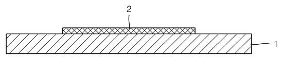
도 1은 본 발명의 일 실시예에 의한 유기 발광 표시 장치를 개략적으로 도시한 단면도이다.
도 2는 도 1의 Ⅱ를 확대한 도면이다.
도 3 내지 도 5는 도 1의 제조 방법을 나타낸 단면도이다.
도 6은 본 발명의 다른 실시예에 의한 유기 발광 표시 장치를 개략적으로 도시한 단면도이다.
도 7는 본 발명의 또 다른 실시예에 의한 유기 발광 표시 장치를 개략적으로 도시한 단면도이다.
도 8는 본 발명의 또 다른 실시예에 의한 유기 발광 표시 장치를 개략적으로 도시한 단면도이다. 1 is a cross-sectional view schematically illustrating an organic light emitting display according to an embodiment of the present invention.
2 is an enlarged view of II in Fig.
3 to 5 are sectional views showing the manufacturing method of Fig.
6 is a cross-sectional view schematically showing an organic light emitting display according to another embodiment of the present invention.
7 is a cross-sectional view schematically showing an organic light emitting display according to another embodiment of the present invention.
8 is a cross-sectional view schematically showing an organic light emitting display according to another embodiment of the present invention.
본 명세서에서는 본 발명을 명확하게 설명하기 위하여 본 발명과 관계없는 부분은 도시 및 기재를 생략하거나, 간략히 기재하거나 도시하였다. 또한, 도면에서는 여러 층 및 영역을 명확하게 표현하기 위하여 두께 및 넓이를 확대하거나, 과장되게 도시하였다. In this specification, parts that are not related to the present invention are omitted or simplified or shown in order to clearly illustrate the present invention. Further, in the drawings, the thickness and the width are enlarged or exaggerated to clearly illustrate the various layers and regions.
본 명세서에서 전체를 통하여 동일 또는 유사한 구성 요소에 대해서는 동일한 도면 부호를 붙였다. 본 명세서에서 “제1”, “제2” 등의 용어는 한정적인 의미가 아니라 하나의 구성 요소를 다른 구성 요소와 구별하는 목적으로 사용되었다. 또한, 막, 영역, 구성 요소 등의 부분이 다른 부분 “위에” 또는 “상에” 있다고 할 때, 다른 부분의 바로 위에 있는 경우뿐만 아니라, 그 중간에 다른 막, 영역, 구성 요소 등이 개재되어 있는 경우도 포함한다. Throughout the specification, the same or similar components are denoted by the same reference numerals. In this specification, terms such as " first ", " second ", and the like are used for the purpose of distinguishing one element from another element. In addition, when a part of a film, an area, a component or the like is referred to as being "on" or "on" another part, not only the part directly above another part but also another film, area, And the like.
이하, 첨부된 도면들에 도시된 본 발명의 바람직한 실시예를 참조하여 본 발명을 보다 상세히 설명한다.Hereinafter, the present invention will be described in more detail with reference to the preferred embodiments of the present invention shown in the accompanying drawings.
도 1은 본 발명의 일 실시예에 의한 유기 발광 표시 장치를 개략적으로 도시한 단면도이다. 도 2는 도 1의 Ⅱ를 확대한 도면이다. 도 3 내지 도 5는 도 1의 제조 방법을 나타낸 단면도이다. 이하에서는 도 1 내지 도 5를 참조하여 본 발명의 일 실시예에 의한 유기 발광 표시 장치의 구조 및 제조 방법을 함께 설명하기로 한다.1 is a cross-sectional view schematically illustrating an organic light emitting display according to an embodiment of the present invention. 2 is an enlarged view of II in Fig. 3 to 5 are sectional views showing the manufacturing method of Fig. Hereinafter, a structure and a manufacturing method of an OLED display according to an embodiment of the present invention will be described with reference to FIGS. 1 to 5. FIG.
도 1 및 도 2를 참조하면, 유기 발광 표시 장치는 기판(1), 기판(1) 상에 구비된 유기 발광부(2) 및 유기 발광부(2)를 밀봉하는 박막 봉지부(10)를 포함한다. 1 and 2, an OLED display includes a
기판(1)은 투명한 플라스틱 또는 투명한 유리 소재를 사용할 수 있다. 기판(1)은 구부러지거나 접히지 않는 리지드(rigid) 특성을 가질 수 있다. 그러나, 기판(1)은 구부러지거나 접힐 수 있는 플렉서블(flexible) 또는 폴더블(foldable) 특성을 가질 수도 있다. 이 경우 기판(1)은 투명한 플라스틱 필름이나 투명한 박막 유리로 이루어질 수 있다. The
유기 발광부(2)는 유기 발광 소자(OLED)를 포함한다. 유기 발광 소자(OLED)는 하부 전극(21), 중간층(23) 및 상부 전극(22)의 적층체를 포함한다. 하부 전극(21)은 도 2에 도시된 바와 같이 각 화소 별로 패터닝되어 아일랜드 형상을 가질 수 있다. 그러나 본 발명은 이에 한정되지 않고 하부 전극(21)은 라인 형상을 가지거나, 면 형상을 가질 수도 있다. The organic
하부 전극(21) 상에는 하부 전극(21)의 가장자리를 덮고 중앙을 노출하는 절연막(24)이 더 구비될 수 있다. The
중간층(23)은 하부 전극(21) 상에 형성되며, 광을 발광하는 유기 발광층을 포함한다. 중간층(23)은 유기물로 이루어진다. 하부 전극(21)이 애노드(anode)로 기능하는 경우, 하부 전극(21)과 유기 발광층 사이에는 순차적으로 정공 주입층(hole injection layer :HIL) 및 정공 수송층(hole transport layer: HTL) 이 배치된다. 또한, 이 경우 상부 전극(22)은 캐소드(cathode)로 기능하게 되므로 유기 발광층과 상부 전극(22) 사이에는 순차적으로 전자 수송층(electron transport layer: ETL) 및 전자 주입층(electron injection layer: EIL)이 배치된다. 물론 유기 발광층에 포함된 유기물의 종류에 따라 기능층의 종류, 순서 및 개수는 달라질 수 있다. 또한, 하부 전극(21) 및 상부 전극(22)의 극성이 반대로 될 수 있다. The
유기 발광층은 화소 별로 패터닝되어 구비될 수 있으며, 도 2와 같이 HIL, HTL, EIL 및기ETL과 같은 기능층은 기판(1) 전체적으로 공통으로 형성될 수 있다. 그러나, 본 발명은 이에 한정되지 않고 유기 발광층이 기판(1) 전체적으로 공통으로 형성될 수도 있다. 예를 들어, 적색, 녹색, 및 청색의 광을 방출하는 복수의 유기 발광층이 수직으로 적층되거나 혼합되어 형성되어 백색광을 방출할 수 있다. 물론, 백색광을 방출하기 위한 색의 조합은 상술한 바에 한정되지 않는다. 한편, 이 경우 방출된 백색광을 소정의 컬러로 변환하는 색변환층이나 컬러필터가 별도로 구비될 수 있다.The organic light emitting layer may be patterned for each pixel, and functional layers such as HIL, HTL, EIL, and ETL may be formed in common throughout the
중간층(23) 상에는 하부 전극(21)과 대향하도록 상부 전극(22)이 형성된다. 상부 전극(22)은 기판(1) 전체적으로 공통으로 형성될 수 있다. 유기 발광 표시 장치가 기판(1)의 방향으로 발광하는 배면 발광형(bottom emission type)인 경우, 하부 전극(21)은 인듐틴옥사이드(ITO)와 같은 투명 도전성 산화물(transparent conductive oxide: TCO)을 이용하여 투명 전극으로 형성하고, 상부 전극(22)은 마그네슘(Mg)과 같은 저저항 금속을 두께를 두껍게 형성하여 반사 전극으로 구현한다. 그런데 유기 발광 표시 장치가 기판(1)의 반대 방향으로 발광하는 전면 발광형(top emission type)인 경우, 하부 전극(21)은 은(Ag)과 같은 반사막을 더 포함하여 반사 전극으로 형성하고, 상부 전극(22)은 저저항 금속의 두께를 얇게 형성하여 반투과 전극으로 구현한다.An
도시되지 않았으나, 상부 전극(22) 상에는 상부 전극(22)을 보호하고, 상면의 평편률(flattening)을 개선하기 위한 목적으로 유기물로 이루어진 보호막을 더 형성할 수 있다. 한편, 유기 발광 표시 장치가 전면 발광 타입인 경우 고굴절률을 가지는 유기막을 포함하는 보호막은 굴절률 매칭 (reflective index matching)을 통해 유기 발광층의 광추출 능력을 향상시키기도 한다. Although not shown, a protective layer made of an organic material may be further formed on the
한편, 도 1 및 도 2에는 도시되지 않았으나, 유기 발광 표시 장치가 능동형(active type) 표시 장치인 경우에는 유기 발광부(2)에 구동 회로부가 더 포함된다. 구동 회로부는 각 유기 발광 소자(LED)에 전기적으로 연결되며 적어도 두 개의 박막 트랜지스터(TFT) 및 적어도 하나의 커패시터를 포함한다. 구동 회로부는 배선으로부터 인가되는 신호에 따라 해당 유기 발광 소자(OLED)로 구동 전류를 인가하여 유기 발광 소자(OLED)를 구동한다. Although not shown in FIGS. 1 and 2, when the OLED display device is an active type display device, the
이하에서는 도 3 내지 도 5를 참조하여, 도 1의 제조 방법을 상세하게 설명한다. Hereinafter, the manufacturing method of FIG. 1 will be described in detail with reference to FIGS. 3 to 5. FIG.
도 3을 참조하면, 기판(1) 상에 먼저 상술한 유기 발광부(2)를 형성한다.Referring to FIG. 3, the organic
이러한 유기 발광부(2)는 외부의 수분 및 산소로부터 보호되어야 한다. 유기 발광 소자(OLED)는 유기물을 포함하고 있으므로 외부의 수분 및 산소에 의해 쉽게 열화(deterioration)된다. 따라서, 유기 발광부(2)를 밀봉하기 위하여 박막 봉지부(10)를 형성한다. 밀봉 구조가 박막 봉지로 구현되는 경우 유기 발광 표시 장치를 쉽게 구부리거나 접을 수 있는 장점이 있다. The organic
본 발명의 일 실시예에 의하면, 박막 봉지부(10)는 무기물로 형성된다. 또한, 박막 봉지부(10)는 복수의 무기막, 예를 들어 두 층의 무기막, 으로 이루어진다. 박막 봉지부(10)는 유기 발광부(2)를 덮어 밀봉하는 제1무기막(11) 및 제1무기막(11)을 덮어 유기 발광부를 밀봉하는 제2무기막(12)을 포함한다. According to one embodiment of the present invention, the thin
제1무기막(11)은 주석산화물, 인산화물, 및 주석불화물을 포함하는 제1무기 혼합물로부터 형성된다. 상술한 제1무기 혼합물은 저온의 점도 변화 온도를 갖는 저온 점도 변화 무기물 (Low temperature Viscosity Transition: LVT)이다. 여기서 “점도 변화 온도”는 상기 LVT 무기물의 점도(Viscosity)가 “고체”에서 “액체”로 완전히 변하는 온도를 의미하는 것은 아니라, 상기 LVT 무기물에 유동성(fluidity)을 제공할 수 있는 최소 온도를 의미한다. The first
제1무기 혼합물의 점도 변화 온도는 유기 발광부(2)의 변성 온도보다 낮은 것을 특징으로 한다. 예를 들어, 제1무기 혼합물의 점도 변화 온도는 섭씨 약 100도 이하인 것을 특징으로 한다. 유기 발광부(2)의 변성 온도란 유기 발광부(2)에 포함된 물질의 변성 온도를 의미한다. 상기 “유기 발광부(2)에 포함된 물질의 변성 온도”란 상기 유기 발광부(2)에 포함된 물질의 화학적 및/또는 물리적 변성을 초래할 수 있는 온도를 의미한다. 예를 들어, 상기 “유기 발광부(2)에 포함된 물질의 변성 온도”는 유기 발광부(2)의 유기막에 포함된 유기물의 유리 전이 온도(Tg)를 의미할 수 있다. 상기 유리 전이 온도는, 예를 들면, 유기 발광부(2)에 포함된 물질에 대하여 TGA(Thermo Gravimetric Analysis) 및 DSC(Differential Scanning Calorimetry)를 이용한 열분석을 수행하여 도출할 수 있으며, 예를 들어 섭씨 약 110도 이상이 될 수 있다. The viscosity change temperature of the first inorganic mixture is lower than the denaturation temperature of the organic
제1무기 혼합물은 주석산화물(예를 들면, SnO 또는 SnO2), 인산화물(예를 들면, P2O5) 및 주석불화물(예를 들면, SnF2)을 포함할 수 있다. 여기서 주석불화물은 약 45몰%(mole%) 내지 85몰% 범위 내에서 포함될 수 있다. 여기서 제1무기 혼합물에 포함된 주석 산화물, 인 산화물 및 주석 불화물 전체의 몰% 합은 100몰%가 되도록 한다. First inorganic mixture may comprise a tin oxide (e.g., SnO or SnO 2), phosphate (e.g., P 2 O 5) and tin fluoride (e.g., SnF 2). Wherein the tin fluoride may be included in the range of about 45 mol% (mole%) to 85 mol%. Here, the mole% sum of the tin oxide, phosphorus oxide and tin fluoride contained in the first inorganic mixture is made to be 100 mol%.
주석불화물은 제1무기 혼합물의 점도 변화 온도를 낮추는 역할을 한다. 만약 주석불화물의 함량이 45몰% 미만인 경우 제1무기 혼합물의 점도 변화 온도가 유기 발광부(2)의 변성 온도보다 높아지는 문제가 있다. 이 후 설명하겠으나 이 경우 힐링(healing) 과정에서 유기 발광부(2)가 손상되는 문제가 있다. 또한, 주석불화물의 함량이 85몰% 초과인 경우 제1무기 혼합물로부터 제1무기막(11)이 형성되지 않는 문제가 있다. 이 후 설명하겠으나 제1무기막(11)은 제1무기 혼합물이 유동성을 가진 후 응고되어 제조되며 이 과정에서 주석산화물 및 인산화물이 큰 기여를 한다. 그러나 주석불화물의 몰%가 85를 초과하는 경우 유도성을 갖는 과정 및 응고 과정이 불완전하게 일어나게 되어 제1무기막(11)의 제조가 불가능하다. Tin fluoride serves to lower the viscosity change temperature of the first inorganic mixture. If the content of tin fluoride is less than 45 mol%, there is a problem that the viscosity change temperature of the first inorganic mixture becomes higher than the denaturation temperature of the organic
제1무기 혼합물은 텅스텐 산화물(예를 들면, WO3), 니오브 산화물(예를 들면, NbO, Nb2O5), 보론 포스페이트(BPO4), 및 납 불화물(예를 들면, PbF2) 중 1종 이상의 첨가 물질을 더 포함할 수 있으나, 이에 한정되는 것은 아니다. 예를 들어 상술한 첨가 물질은 약 5몰%를 넘지 않는 것이 바람직하다. 이러한 첨가 물질은 제1무기막(11)의 내구성 및 투과도를 개선하며 표면 강도를 조절할 수 있고, 제1무기막(11)의 열팽창계수(COEFFICIENT OF THERMAL EXPANSION: CTE) 및 영률(young`s modulus)를 조절할 수 있다.First inorganic mixture of tungsten oxide (for example, WO 3), niobium oxide (e.g., NbO, Nb 2 O 5) , boron phosphate (BPO 4), and lead fluoride (e.g., PbF 2) of But it is not limited thereto. For example, it is preferred that the above-mentioned additive material does not exceed about 5 mol%. These additives can improve the durability and permeability of the first
한편, 제1무기 혼합물을 하기 표 1에 도시된 조성비를 가질 수 있다. 표 1에는 제1무기 혼합물의 조성비에 따른 점도 변화 온도의 측정 값을 함께 기록하였다. On the other hand, the first inorganic mixture may have a composition ratio shown in Table 1 below. In Table 1, measured values of the viscosity change temperature according to the composition ratio of the first inorganic mixture were also recorded.
(mole%)SnO
(mole%)
(mole%)SnF 2
(mole%)
(mole%)P 2 O 5
(mole%)
(mole%)WO 3
(mole%)
(℃)Viscosity change temperature
(° C)
이하에서 제1무기막(11)을 형성하는 과정과 함께 제1무기막(11)의 특징도 함께 설명한다. Hereinafter, the process of forming the first
먼저, 유기 발광부(1)를 덮도록 제1무기 혼합물을 제공하여 제1예비-무기막(미도시)을 형성한다. First, a first inorganic mixture is provided to cover the organic
제1예비-무기막은 제1무기 혼합물을 스퍼터링 방법으로 제공하여 형성할 수 있다. 구체적으로, SnO-SnF2-P2O5-WO3 조성의 무기물을 스퍼터링 방식을 통해 성막할 수 있다. 스퍼터링 방식은 구체적으로 듀얼 로터리 타겟(dual rotary target)방식 또는 직류 펄스(DC Pulse) 전원을 이용한 페이싱 타겟(Facing Target) 방식을 적용하고, 기판이 움직이면서 스캔하는 방식을 사용할 수 있다. 4kW~20kW 및 0.3Pa~1.5Pa의 아르곤 플라즈마를 사용할 수 있으며, 복수 회의 스캔 반복으로 원하는 막 두께를 얻을 수 있다. 이렇게 대략 1㎛ 두께의 제1무기막을 얻을 수 있다. The first pre-inorganic film may be formed by providing a first inorganic mixture by a sputtering method. Specifically, an inorganic material having a composition of SnO-SnF 2 -P 2 O 5 -WO 3 can be formed by a sputtering method. As the sputtering method, a Facing Target method using a dual rotary target method or a DC pulse power source may be applied, and a method of scanning the substrate while moving can be used. Argon plasma of 4 kW to 20 kW and 0.3 Pa to 1.5 Pa can be used and a desired film thickness can be obtained by repeating a plurality of scans. Thus, a first inorganic film having a thickness of approximately 1 mu m can be obtained.
그러나, 제1예비-무기막을 형성하는 방법은 이에 한정되지 않고, 제1무기 혼합물을 증발법(evaporation), 진공 증착법, 저온 증착법, 플라즈마 강화 화학적 기상 증착법(PCVD), 플라즈마 이온 지원 증착법(PIAD), 슬릿 코팅법(slit coating), 플래시 증착법(flash evaporator), 전자 빔 코팅법 또는 이온 플레이팅법 등의 방법을 사용할 수도 있다. However, the method of forming the first pre-inorganic film is not limited thereto, and the first inorganic mixture may be formed by evaporation, vacuum deposition, low temperature deposition, plasma enhanced chemical vapor deposition (PCVD), plasma ion assisted deposition (PIAD) A slit coating method, a flash evaporator method, an electron beam coating method, or an ion plating method may be used.
다음으로, 제1예비 무기막을 힐링 한다. Next, the first preliminary inorganic film is healed.
힐링 단계는 상기 제1무기-혼합물의 점도 변화 온도 이상 내지 상기 유기 발광부의 변성 온도 미만의 온도 범위에서 제1예비-무기막을 열처리함으로써 수행된다. 상기 제1무기-혼합물의 점도 변화 온도는 주석불화물의 함량 등에 의해 달라질 수 있을 것이다. 예를 들어, 상기 표 1을 참조하면 열처리는 섭씨 약 71도 이상에서 100도 미만의 온도 범위에서 약 1시간 내지 3시간 가량 수행될 수 있다. 힐링 단계의 온도가 상술한 범위 내에서 이루어짐으로써, 제1예비-무기막의 유동화가 가능해지고, 유기 발광부의 변성이 방지될 수 있다. 힐링 단계는 제1예비-무기막에 있는 핀홀(pin hole)을 통한 유기 발광부의 외부 환경 노출을 방지하기 위하여 진공 분위기 또는 블활성 가스 분위기, 예를 들면 아르곤(Ar) 분위기, 하에서 적외선(IR) 오븐에 의해 수행될 수 있다. 그러나 반드시 이에 한정되는 것은 아니고 레이저 스캐닝에 의해 힐링 공정을 진행할 수 있다.The healing step is performed by heat-treating the first pre-inorganic film at a temperature ranging from a viscosity change temperature of the first inorganic-mixture to a temperature lower than a denaturation temperature of the organic light emitting portion. The viscosity change temperature of the first inorganic-mixture may vary depending on the content of tin fluoride and the like. For example, referring to Table 1 above, the heat treatment may be performed for about 1 to 3 hours at a temperature range of from about 71 degrees Celsius to less than 100 degrees Celsius. By making the temperature of the healing step within the above-mentioned range, fluidization of the first pre-inorganic film becomes possible, and denaturation of the organic light emitting portion can be prevented. In the healing step, infrared (IR) light is irradiated under a vacuum atmosphere or an inert gas atmosphere such as argon (Ar) atmosphere in order to prevent exposure of the organic light emitting portion through a pin hole in the first pre- Can be performed by an oven. However, the present invention is not limited thereto, and the healing process can be performed by laser scanning.
이러한 힐링 단계에 의하여, 제1 예비-무기막에 포함된 제1혼합 무기물은 유동화(fluidized)될 수 있다. 유동화된 제1혼합 무기물은 흐름성(flowability)를 가질 수 있다. 따라서, 상기 힐링 단계시, By this healing step, the first mixed inorganic material contained in the first pre-inorganic film can be fluidized. The fluidized first mixed inorganic material may have flowability. Therefore, during the healing step,
1) 환경성 요소(15)와 유기 발광부(2) 사이의 빈 공간에 유동화된 제1혼합 무기물이 흘러 충진될 수 있다. 여기서 환경성 요소(15)란 유기 발광부 형성시 존재 및 생성되는 필수불가결한 불순물 입자로서, 예를 들면, 외부 환경으로부터 유입된 미세 입자(예를 들면, 외부 환경에 존재하는 먼지, 티끌 등), 유기 발광부 형성시 사용된 물질로서 유기 발광부(2) 상에 잔류하는 미세 입자(예를 들면, 상부 전극(22) 성막 후 잔류하는 상부 전극(22) 형성용 물질로 이루어진 미세 입자 등) 등일 수 있다. 상기 환경성 요소(15)의 성분은 각종 유기물, 무기물, 유무기/복합체일 수 있는 등 매우 다양하다. 1) The first mixed inorganic material fluidized in the void space between the
2) 제1예비-무기막 중 핀홀에 유동화된 제1혼합 무기물이 흘러 충진될 수 있다. 2) The first mixed inorganic material fluidized in the pinhole of the first pre-inorganic film may flow and be filled.
힐링 단계 후 유동화된 제1혼합 무기물을 응고되어 막질이 치밀한 제1무기막(11)이 형성된다. 이로써 제1무기막(11)은 핀홀이 존재하지 않는 치밀한 막질을 가지게 된다. 핀홀은 외부의 수분 및 산소의 이동 통로가 되어 유기 발광 표시 장치에 진행성 암점을 발생시키고 박막 봉지를 수축시키는 등 유기 발광 장치의 수명을 저하시킬 수 있는 요소이다. 또한, 제1무기막(11)은 환경적 요소(150의 외면을 완전히 덮어 환경적 요소(15)에 의해 발생한 간극으로 외부의 수분 및 산소가 침투하는 것을 막을 수 있다. After the healing step, the fluidized first mixed inorganic material is solidified to form a dense first
이와 같이 본 발명의 일 실시예에 의하면, 유기 발광부(2)와 직접 접촉하는 제1무기막(11)의 경우 유기 발광부(2)의 변성 온도보다 낮은 온도에서 유동성을 가질 수 있는 제1혼합 무기물을 이용하여 힐링 공정을 통해 형성함으로써, 유기 발광부(2)의 손상 없이도 결함이 없고 막질이 치밀한 제1무기막(11)을 얻을 수 있다. The first
그러나, 제1무기막(11)은 주석불화물을 포함하기 때문에 다음과 같은 문제가 발생한다. 주석불화물은 제1무기막(11)의 점도 변화 온도를 낮추는데 기여하지만, 수분과 반응성이 좋은 특징이 있다. 따라서, 제1무기막(11) 만으로 박막 봉지부(10)를 구현하는 경우 시간이 지남에 따라 외부의 수분에 의해 박막 봉지부(10)의 배리어(barrier) 특성이 나빠진다. 따라서, 본 발명의 일 실시예에 의하면, 제1무기막(11) 상에 배리어 특성이 좋은 제2 무기막(12)을 추가로 형성한다. However, since the first
제2무기막(12)은 주석산화물(예를 들면, SnO 또는 SnO2) 및 인산화물(예를 들면, P2O5)을 포함한다. 제2무기막(12)은 주석불화물(예를 들면, SnF2)을 포함하지 않는다. 주석산화물 및 인산화물은 수분 및 산소와 반응성이 없거나 아주 작기 때문에 외부의 수분 및 산소에 대한 배리어 특성이 좋다. The second
제2무기막(12)은 텅스텐 산화물(예를 들면, WO3), 니오브 산화물(예를 들면, NbO, Nb2O5), 보론 포스페이트(BPO4), 및 납 불화물(예를 들면, PbF2) 중 1종 이상의 첨가 물질을 더 포함할 수 있으나, 이에 한정되는 것은 아니다. The second
주석산화물 및 인산화물을 포함하는 제2무기 혼합물도 저온 점도 변화 무기물 (Low temperature Viscosity Transition: LVT)이다. 그런데, 제2무기 혼합물의 경우 점도 변화 온도가 유기 발광부의 변성 온도보다 높을 수 있다. 따라서, 제2무기막(12)은 힐링 공정을 수행하지 않는다. The second inorganic mixture comprising tin oxide and phosphorous is also a low temperature Viscosity Transition (LVT). However, in the case of the second inorganic mixture, the viscosity change temperature may be higher than the denaturation temperature of the organic light emitting portion. Therefore, the second
한편, 제2무기 혼합물을 하기 표 2에 도시된 조성비를 가질 수 있다. 표 2에는 제2무기 혼합물의 조성비에 따른 배리어 특성의 측정 값도 함께 기록하였다. 참고로, 배리어 특성은 섭씨 약 85도의 온도 및 약 85% 습도의 고온 고습한 환경에서 하기 조성을 가지는 제2무기막(12)을 박막 봉지부로 포함하는 유기 발광 표시 장치 샘플을 약 1000시간(hr)동안 노출하였다. 그리고 유기 발광 표시 장치에 암점이 발생하거나, 화소의 수축 및 변형이 발생하였는지 확인하였다. 표 2에 도시된 바와 같이 제2무기막(12)은 고온 고습한 환경에서도 우수한 배리어 특성을 유지하는 것으로 판단된다. On the other hand, the second inorganic mixture may have a composition ratio shown in Table 2 below. Table 2 also shows the measured values of the barrier characteristics according to the composition ratio of the second inorganic compound. For reference, the barrier property was measured at about 1000 hours (hr) in a sample of the organic light emitting display including the second
(mole%)SnO
(mole%)
(mole%)P 2 O 5
(mole%)
아래에서는 상술한 제2무기막의 제조 과정을 설명한다. The manufacturing process of the above-described second inorganic film will be described below.
다시 도 1을 참조하면, 제1무기막(11)을 덮도록 제2무기 혼합물을 제공하여 제2무기막(12)을 형성한다. Referring again to FIG. 1, the second
제2무기막(12)은 제2무기 혼합물을 스퍼터링 방법으로 제공하여 형성할 수 있다. 구체적으로, SnO-P2O5 조성의 무기물을 스퍼터링 방식을 통해 성막할 수 있다. 스퍼터링 방식은 상술한 제1예비-무기막에서 채용한 것과 동일하거나 유사할 수 있다. The second
한편, 제2무기막(12)을 형성하는 방법은 이에 한정되지 않고, 제2무기 혼합물을 증발법(evaporation), 진공 증착법, 저온 증착법, 플라즈마 강화 화학적 기상 증착법(PCVD), 플라즈마 이온 지원 증착법(PIAD), 슬릿 코팅법(slit coating), 플래시 증착법(flash evaporator), 전자 빔 코팅법 또는 이온 플레이팅법 등의 방법을 사용할 수도 있다. The method of forming the second
제2무기막(12)은 제1무기막(11)과 달리 힐링 공정은 진행하지 않는다. 따라서, 제2무기막(12)에 비해 제1무기막(11)의 막질이 더 치밀할 수 밖에 없다. Unlike the first
본 발명의 일 실시예에 의하면, 박막 봉지부(10)가 제1무기막(11) 및 제2무기막(12)을 포함하도록 형성함으로써, 강건한 밀봉 구조를 구현할 수 있다. 제1무기막(11)은 유기 발광부(2)를 변성 시키지 않으면서 용융 및 응고되어 치밀한 막질을 가지며 환경적 요소를 매립할 수 있다. 또한 제2무기막(12)은 제1무기막(11)에 비해 수분 및 산소와 반응성이 좋지 않아 배리어 특성이 우수하다.
According to the embodiment of the present invention, the
도 6은 본 발명의 다른 실시예에 의한 유기 발광 표시 장치를 개략적으로 도시한 단면도이다. 6 is a cross-sectional view schematically showing an organic light emitting display according to another embodiment of the present invention.
도 6을 참조하면 도 1의 실시예에 비하여 유기 발광부(2)와 제1무기막(11) 사이에 하부막(13)이 더 형성된 것을 특징으로 한다. 하부막(13)은 유기 발광부(2) 상에 직접 형성되어 표면을 평탄화한다. 또한 하부막(13)은 유기 발광부(2)의 상면과 제1무기막(11) 간의 열팽창계수 차이에 의해 계면 접착력이 약화되는 것을 방지하기 위해 열팽창계수 매칭 기능을 하여 유기 발광부(2)와 제1무기막(11)의 계면 접착력을 강화할 수 있다. 그 외에도 스퍼터링으로 제1예비-무기막을 형성하는 과정에서 하부막(13)은 유기 발광부(2)의 상면, 예를 들어 상부 전극(22)이나 보호막, 이 손상되는 것을 방지한다. Referring to FIG. 6, a
하부막(13)은 무기물질 또는 유기물질 중 하나 이상을 포함하도록 형성될 수 있으며, 단일층 또는 다층으로 형성될 수 있다. 예를 들어 하부막(13)은 텅스텐산화물, 실리콘질화물, 실리콘화합물 및 각종 고분자 물질의 단량체(monomer) 중 적어도 하나를 포함할 수 있다. The
하부막(13)은 각종 코팅 방법, 화학 기상 증착(CVD) 방법, 증발법(evaporation), 진공 증착법, 저온 증착법 등의 방법으로 형성될 수 있으나, 이에 한정된 것은 아니다.
The
도 7는 본 발명의 또 다른 실시예에 의한 유기 발광 표시 장치를 개략적으로 도시한 단면도이다. 7 is a cross-sectional view schematically showing an organic light emitting display according to another embodiment of the present invention.
도 7을 참조하면 도 1의 실시예에 비하여 제1무기막(11)과 제2무기막(12) 사이에 중간막(14)이 더 형성된 것을 특징으로 한다. 중간막(14)은 제1무기막(11)을 형성한 후 제2무기막(12)을 형성하기 전에 산소 및 수분으로부터 제1무기막(11)을 보호한다. 또한, 제1무기막(11)과 제2무기막(12) 간의 열팽창 계수 차이에 의해 계면 접착력이 약화되는 것을 방지하기 위해 열팽창 계수 매칭 기능을 하여 제1무기막(11)과 제2무기막(12)의 계면 접착력을 강화할 수 있다. Referring to FIG. 7, an
하부막(13)과 마찬가지로 중간막(14)은 무기물질 또는 유기물질 중 하나 이상을 포함하도록 형성될 수 있으며, 단일층 또는 다층으로 형성될 수 있다. 예를 들어 중간막(14)은 텅스텐산화물, 실리콘질화물, 실리콘화합물 및 각종 고분자 물질의 단량체(monomer) 중 적어도 하나를 포함할 수 있다.Like the
중간막(14)은 각종 코팅 방법, 화학기상증착 방법, 증발법(evaporation), 진공 증착법, 저온 증착법 등의 방법으로 형성될 수 있으나, 이에 한정된 것은 아니다.The
도 8는 본 발명의 또 다른 실시예에 의한 유기 발광 표시 장치를 개략적으로 도시한 단면도이다. 8 is a cross-sectional view schematically showing an organic light emitting display according to another embodiment of the present invention.
도 8은 도 6의 실시예 및 도 7의 실시예를 결합한 것으로, 유기 발광부(2)와 제1무기막(11) 사이에 하부막(13)이 배치되며, 제1무기막(11)과 제2무기막(12) 사이에 중간막(14)이 배치된다. 하부막(13) 및 중간막(14)의 형태, 구성, 제조 방법, 재료, 기능 및 특징은 상술하였으므로 중복되는 설명은 생략한다. 8 is a view showing a state in which the
본 발명은 첨부된 도면에 도시된 일 실시예를 참고로 설명되었으나 이는 예시적인 것에 불과하며, 당해 기술분야에서 통상의 지식을 가진 자라면 이로부터 다양한 변형 및 균등한 타 실시예가 가능하다는 점을 이해할 수 있을 것이다. 따라서 본 발명의 진정한 보호 범위는 첨부된 청구 범위에 의해서만 정해져야 할 것이다.While the present invention has been particularly shown and described with reference to exemplary embodiments thereof, it is clearly understood that the same is by way of illustration and example only and is not to be taken by way of limitation and that those skilled in the art will recognize that various modifications and equivalent arrangements may be made therein. It will be possible. Accordingly, the true scope of protection of the present invention should be determined only by the appended claims.
1: 기판
2: 유기 발광부
11: 제1무기막
12: 제2무기막
13: 하부막
14: 중간막
15: 환경성 요소1: substrate
2: organic light emitting portion
11: First inorganic film
12: Second inorganic film
13:
14: Middle membrane
15: Environmental factors
Claims (20)
기판 상에 위치하며 제1전극, 유기 발광층, 및 제2전극의 적층체를 포함하는 유기 발광부;
상기 유기 발광부를 덮으며 주석산화물, 인산화물 및 주석불화물을 포함하는 제1무기 혼합물로부터 형성된 제1무기막; 및
상기 제1무기막을 덮으며 주석산화물 및 인산화물을 포함하는 제2무기막;
을 포함하는, 유기 발광 표시 장치.Board;
An organic light emitting display comprising: a substrate; a first electrode; an organic light emitting layer; and a second electrode;
A first inorganic film formed from a first inorganic mixture covering the organic light emitting portion and including tin oxide, phosphorus oxide and tin fluoride; And
A second inorganic film covering the first inorganic film and containing tin oxide and phosphorous;
And an organic light emitting diode.
상기 제1무기 혼합물의 점도 변화 온도는 상기 유기 발광부의 변성 온도보다 낮은, 유기 발광 표시 장치.The method according to claim 1,
Wherein the viscosity change temperature of the first inorganic mixture is lower than the denaturation temperature of the organic light emitting portion.
상기 제1무기 혼합물 중 상기 주석불화물은 45몰%(mole%) 내지 85몰%(mole%) 범위 내에서 포함되는, 유기 발광 표시 장치.The method according to claim 1,
Wherein the tin fluoride in the first inorganic mixture is contained in a range of 45 mol% (mole%) to 85 mol% (mole%).
상기 제1무기막은 상기 제2무기막에 비해 막질이 치밀한, 유기 발광 표시 장치. The method according to claim 1,
Wherein the first inorganic film is dense in film quality as compared with the second inorganic film.
상기 제1무기막은 환경성 요소의 외면을 덮는, 유기 발광 표시 장치.The method according to claim 1,
Wherein the first inorganic film covers an outer surface of the environmental element.
상기 제2무기막은 상기 제1무기막에 비해 수분 반응성이 작은, 유기 발광 표시 장치.The method according to claim 1,
Wherein the second inorganic film has a smaller moisture reactivity than the first inorganic film.
상기 제1무기 혼합물 및 상기 제2무기막에는
보론포스페이트, 니오브산화물, 텅스텐산화물, 보론산화물 및 납불화물 중 적어도 하나 이상이 더 포함되는, 유기 발광 표시 장치.The method of claim 1, wherein
Wherein the first inorganic mixture and the second inorganic film
Wherein at least one of boron phosphate, niobium oxide, tungsten oxide, boron oxide, and lead fluoride is further included.
상기 유기 발광부와 상기 제1무기막 사이에 개재되며 유기물질 또는 무기물질을 포함하는 하부막;
을 더 포함하는, 유기 발광 표시 장치.The method of claim 1, wherein
A lower film interposed between the organic light emitting portion and the first inorganic film and including an organic material or an inorganic material;
Further comprising an organic light emitting diode.
상기 제1무기막과 상기 제2무기막 사이에 개재되며 유기물질 또는 무기물질을 포함하는 중간막;
을 더 포함하는, 유기 발광 표시 장치.The method of claim 1, wherein
An intermediate film interposed between the first inorganic film and the second inorganic film and including an organic material or an inorganic material;
Further comprising an organic light emitting diode.
상기 유기 발광부와 상기 제1무기막 사이에 개재되며 유기물질 또는 무기물질을 포함하는 하부막; 및
상기 제1무기막과 상기 제2무기막 사이에 개재되며 유기물질 또는 무기물질을 포함하는 중간막;
을 더 포함하는, 유기 발광 표시 장치.The method of claim 1, wherein
A lower film interposed between the organic light emitting portion and the first inorganic film and including an organic material or an inorganic material; And
An intermediate film interposed between the first inorganic film and the second inorganic film and including an organic material or an inorganic material;
Further comprising an organic light emitting diode.
상기 유기 발광부를 덮으며 주석산화물, 인산화물 및 주석불화물을 포함하는 제1무기 혼합물로부터 제1무기막을 형성하는 단계; 및
상기 제1무기막을 덮으며 주석산화물 및 인산화물을 포함하는 제2무기막을 형성하는 단계;
을 포함하는, 유기 발광 표시 장치의 제조 방법.Forming an organic light emitting portion including a laminate of a first electrode, an organic light emitting layer, and a second electrode on a substrate;
Forming a first inorganic film from the first inorganic mixture covering the organic light emitting portion and including tin oxide, phosphorus oxide and tin fluoride; And
Forming a second inorganic film covering the first inorganic film and including tin oxide and phosphorous oxide;
Wherein the organic light emitting display device comprises a light emitting diode.
상기 제1무기막을 형성하는 단계는,
상기 제1무기 혼합물을 상기 유기 발광부 상에 제공하여 제1예비-무기막을 형성하는 단계;
상기 제1예비-무기막을 상기 제1무기 혼합물의 점도 변화 온도 이상 상기 유기 발광부의 변성 온도 미만의 온도에서 열처리하는 단계; 및
열처리된 상기 제1예비-무기막이 응고되어 상기 제1무기막을 형성하는 단계;
를 포함하는, 유기 발광 표시 장치의 제조 방법.12. The method of claim 11,
Wherein the forming of the first inorganic film comprises:
Providing the first inorganic mixture on the organic light emitting portion to form a first pre-inorganic film;
Heat-treating the first pre-inorganic film at a temperature higher than a viscosity change temperature of the first inorganic mixture at a temperature lower than a modifying temperature of the organic light emitting portion; And
The heat-treated first pre-inorganic film is solidified to form the first inorganic film;
Emitting device.
상기 제1예비-무기막을 형성하는 단계는,
상기 제1무기 혼합물을 상기 유기 발광부 상에 스퍼터링 방법으로 제공하는, 유기 발광 표시 장치의 제조 방법.13. The method of claim 12,
The step of forming the first pre-
Wherein the first inorganic mixture is provided on the organic light emitting portion by a sputtering method.
상기 제1무기 혼합물 중 상기 주석불화물은 45몰%(mole%) 내지 85몰%(mole%) 범위 내에서 포함되는, 유기 발광 표시 장치의 제조 방법.12. The method of claim 11,
Wherein the tin fluoride in the first inorganic mixture is contained in a range of 45 mol% (mole%) to 85 mol% (mole%).
상기 제2무기막을 형성하는 단계는,
상기 주석산화물 및 인산화물을 상기 제1무기막 상에 스퍼터링 방법으로 제공하는, 유기 발광 표시 장치의 제조 방법.12. The method of claim 11,
Wherein the forming of the second inorganic film comprises:
Wherein the tin oxide and the phosphorous oxide are provided on the first inorganic film by a sputtering method.
상기 제2무기막은 상기 제1무기막에 비해 수분 반응성이 작은, 유기 발광 표시 장치의 제조 방법.12. The method of claim 11,
Wherein the second inorganic film has a smaller moisture reactivity than the first inorganic film.
상기 제1무기 혼합물 및 상기 제2무기막에는
보론포스페이트, 니오브산화물, 텅스텐산화물, 보론산화물 및 납불화물 중 적어도 하나 이상이 더 포함되는, 유기 발광 표시 장치의 제조 방법.The method of claim 11, wherein
Wherein the first inorganic mixture and the second inorganic film
Wherein at least one of boron phosphate, niobium oxide, tungsten oxide, boron oxide, and lead fluoride is further included.
상기 유기 발광부와 상기 제1무기막 사이에 유기물질 또는 무기물질을 포함하는 하부막을 형성하는 단계;
을 더 포함하는, 유기 발광 표시 장치의 제조 방법.The method of claim 11, wherein
Forming a lower film including an organic material or an inorganic material between the organic light emitting portion and the first inorganic film;
Wherein the organic light emitting display device further comprises:
상기 제1무기막과 상기 제2무기막 사이에 유기물질 또는 무기물질을 포함하는 중간막을 형성하는 단계;
을 더 포함하는, 유기 발광 표시 장치의 제조 방법.The method of claim 11, wherein
Forming an interlayer including an organic material or an inorganic material between the first inorganic film and the second inorganic film;
Wherein the organic light emitting display device further comprises:
상기 유기 발광부와 상기 제1무기막 사이에 유기물질 또는 무기물질을 포함하는 하부막을 형성하는 단계; 및
상기 제1무기막과 상기 제2무기막 사이에 유기물질 또는 무기물질을 포함하는 중간막을 형성하는 단계;
을 더 포함하는, 유기 발광 표시 장치의 제조 방법.The method of claim 11, wherein
Forming a lower film including an organic material or an inorganic material between the organic light emitting portion and the first inorganic film; And
Forming an interlayer including an organic material or an inorganic material between the first inorganic film and the second inorganic film;
Wherein the organic light emitting display device further comprises:
Priority Applications (4)
| Application Number | Priority Date | Filing Date | Title |
|---|---|---|---|
| KR1020130036439A KR20140120541A (en) | 2013-04-03 | 2013-04-03 | Organic light emitting device display and manufacturing method thereof |
| US13/972,870 US9196863B2 (en) | 2013-04-03 | 2013-08-21 | Organic light emitting display device and method of manufacturing the same |
| TW102139292A TW201440278A (en) | 2013-04-03 | 2013-10-30 | Organic light emitting display device and method of manufacturing the same |
| CN201310571210.1A CN104103664A (en) | 2013-04-03 | 2013-11-13 | Organic light emitting display device and method of manufacturing the same |
Applications Claiming Priority (1)
| Application Number | Priority Date | Filing Date | Title |
|---|---|---|---|
| KR1020130036439A KR20140120541A (en) | 2013-04-03 | 2013-04-03 | Organic light emitting device display and manufacturing method thereof |
Publications (1)
| Publication Number | Publication Date |
|---|---|
| KR20140120541A true KR20140120541A (en) | 2014-10-14 |
Family
ID=51653837
Family Applications (1)
| Application Number | Title | Priority Date | Filing Date |
|---|---|---|---|
| KR1020130036439A KR20140120541A (en) | 2013-04-03 | 2013-04-03 | Organic light emitting device display and manufacturing method thereof |
Country Status (4)
| Country | Link |
|---|---|
| US (1) | US9196863B2 (en) |
| KR (1) | KR20140120541A (en) |
| CN (1) | CN104103664A (en) |
| TW (1) | TW201440278A (en) |
Cited By (1)
| Publication number | Priority date | Publication date | Assignee | Title |
|---|---|---|---|---|
| KR20170006344A (en) * | 2015-07-07 | 2017-01-18 | 삼성디스플레이 주식회사 | Organic light-emitting display apparatus and manufacturing the same |
Families Citing this family (8)
| Publication number | Priority date | Publication date | Assignee | Title |
|---|---|---|---|---|
| KR20140120541A (en) * | 2013-04-03 | 2014-10-14 | 삼성디스플레이 주식회사 | Organic light emitting device display and manufacturing method thereof |
| KR102192035B1 (en) * | 2013-12-02 | 2020-12-17 | 삼성디스플레이 주식회사 | Flexible display device including touch detecting sensor |
| CN105938875B (en) * | 2016-07-12 | 2018-08-14 | 深圳市华星光电技术有限公司 | WOLED device architectures and display device |
| CN108470755B (en) * | 2017-03-21 | 2020-07-24 | 京东方科技集团股份有限公司 | Thin film packaging structure, thin film packaging method and display device |
| JP6762912B2 (en) | 2017-06-26 | 2020-09-30 | 双葉電子工業株式会社 | Organic EL display device |
| CN109148728B (en) * | 2018-08-31 | 2019-10-29 | 昆山国显光电有限公司 | A kind of display panel and display device |
| CN109728189B (en) * | 2018-11-26 | 2021-01-22 | 云谷(固安)科技有限公司 | Display panel and display device |
| CN109671758A (en) * | 2018-12-18 | 2019-04-23 | 武汉华星光电半导体显示技术有限公司 | Display panel and preparation method thereof, display device |
Family Cites Families (32)
| Publication number | Priority date | Publication date | Assignee | Title |
|---|---|---|---|---|
| US6881447B2 (en) * | 2002-04-04 | 2005-04-19 | Dielectric Systems, Inc. | Chemically and electrically stabilized polymer films |
| US6879319B2 (en) * | 2002-10-25 | 2005-04-12 | Eastman Kodak Company | Integrated OLED display and touch screen |
| US7722929B2 (en) * | 2005-08-18 | 2010-05-25 | Corning Incorporated | Sealing technique for decreasing the time it takes to hermetically seal a device and the resulting hermetically sealed device |
| US7829147B2 (en) * | 2005-08-18 | 2010-11-09 | Corning Incorporated | Hermetically sealing a device without a heat treating step and the resulting hermetically sealed device |
| US20070040501A1 (en) | 2005-08-18 | 2007-02-22 | Aitken Bruce G | Method for inhibiting oxygen and moisture degradation of a device and the resulting device |
| US20080206589A1 (en) * | 2007-02-28 | 2008-08-28 | Bruce Gardiner Aitken | Low tempertature sintering using Sn2+ containing inorganic materials to hermetically seal a device |
| US7663312B2 (en) * | 2006-07-24 | 2010-02-16 | Munisamy Anandan | Flexible OLED light source |
| US7615506B2 (en) * | 2006-10-06 | 2009-11-10 | Corning Incorporated | Durable tungsten-doped tin-fluorophosphate glasses |
| US8115326B2 (en) * | 2006-11-30 | 2012-02-14 | Corning Incorporated | Flexible substrates having a thin-film barrier |
| US20080290798A1 (en) | 2007-05-22 | 2008-11-27 | Mark Alejandro Quesada | LLT barrier layer for top emission display device, method and apparatus |
| CN101970220B (en) * | 2008-03-19 | 2014-10-29 | 柯尼卡美能达精密光学株式会社 | Method for producing molded body or wafer lens |
| US8563113B2 (en) * | 2010-04-20 | 2013-10-22 | Corning Incorporated | Multi-laminate hermetic barriers and related structures and methods of hermetic sealing |
| US20120028011A1 (en) * | 2010-07-27 | 2012-02-02 | Chong Pyung An | Self-passivating mechanically stable hermetic thin film |
| US10158057B2 (en) * | 2010-10-28 | 2018-12-18 | Corning Incorporated | LED lighting devices |
| KR101775659B1 (en) | 2010-12-30 | 2017-09-06 | 서울반도체 주식회사 | Light emitting device having wavelength converting layer |
| KR101347541B1 (en) * | 2012-03-02 | 2014-01-06 | 삼성디스플레이 주식회사 | Method for preparing organic light emitting device |
| KR101931177B1 (en) * | 2012-03-02 | 2018-12-21 | 삼성디스플레이 주식회사 | Organic light emitting display device |
| KR101503401B1 (en) * | 2012-03-05 | 2015-03-17 | 삼성디스플레이 주식회사 | Method for preparing organic light emitting device |
| KR101333138B1 (en) * | 2012-03-05 | 2013-11-26 | 삼성디스플레이 주식회사 | Method for preparing organic light emitting device, substrate for transiting of an inorganic film and organic light emitting device |
| TW201343940A (en) * | 2012-03-14 | 2013-11-01 | Corning Inc | Sputtering targets and associated sputtering methods for forming hermetic barrier layers |
| KR101923176B1 (en) * | 2012-06-11 | 2018-11-29 | 삼성디스플레이 주식회사 | Flat panel display device and manufacturing method thereof |
| US20140120315A1 (en) * | 2012-10-25 | 2014-05-01 | Bruce Gardiner Aitken | Flexible multilayer hermetic laminate |
| US10017849B2 (en) * | 2012-11-29 | 2018-07-10 | Corning Incorporated | High rate deposition systems and processes for forming hermetic barrier layers |
| US9666763B2 (en) * | 2012-11-30 | 2017-05-30 | Corning Incorporated | Glass sealing with transparent materials having transient absorption properties |
| US9202996B2 (en) * | 2012-11-30 | 2015-12-01 | Corning Incorporated | LED lighting devices with quantum dot glass containment plates |
| US20140151721A1 (en) * | 2012-11-30 | 2014-06-05 | Corning Incorporated | Phase transition cooling in led lighting devices |
| US8754434B1 (en) * | 2013-01-28 | 2014-06-17 | Corning Incorporated | Flexible hermetic thin film with light extraction layer |
| KR102036327B1 (en) * | 2013-03-27 | 2019-11-27 | 삼성디스플레이 주식회사 | Organic luminescence emitting display device and method for manufacturing the same |
| KR20140120541A (en) * | 2013-04-03 | 2014-10-14 | 삼성디스플레이 주식회사 | Organic light emitting device display and manufacturing method thereof |
| KR102072805B1 (en) * | 2013-04-15 | 2020-02-04 | 삼성디스플레이 주식회사 | Organic luminescence emitting display device and method for preparing the same |
| KR102072806B1 (en) * | 2013-04-18 | 2020-03-03 | 삼성디스플레이 주식회사 | Organic light emitting display device and method of manufacturing the same |
| KR20140129770A (en) * | 2013-04-30 | 2014-11-07 | 삼성디스플레이 주식회사 | Tablet for plasma coating system, manufacturing method of the same, and manufacturing method of thin film using the same |
-
2013
- 2013-04-03 KR KR1020130036439A patent/KR20140120541A/en not_active Application Discontinuation
- 2013-08-21 US US13/972,870 patent/US9196863B2/en not_active Expired - Fee Related
- 2013-10-30 TW TW102139292A patent/TW201440278A/en unknown
- 2013-11-13 CN CN201310571210.1A patent/CN104103664A/en active Pending
Cited By (2)
| Publication number | Priority date | Publication date | Assignee | Title |
|---|---|---|---|---|
| KR20170006344A (en) * | 2015-07-07 | 2017-01-18 | 삼성디스플레이 주식회사 | Organic light-emitting display apparatus and manufacturing the same |
| US11316133B2 (en) | 2015-07-07 | 2022-04-26 | Samsung Display Co., Ltd. | Organic light-emitting display apparatus and manufacturing method of the same |
Also Published As
| Publication number | Publication date |
|---|---|
| TW201440278A (en) | 2014-10-16 |
| CN104103664A (en) | 2014-10-15 |
| US9196863B2 (en) | 2015-11-24 |
| US20140299847A1 (en) | 2014-10-09 |
Similar Documents
| Publication | Publication Date | Title |
|---|---|---|
| KR20140120541A (en) | Organic light emitting device display and manufacturing method thereof | |
| KR101970361B1 (en) | Organic light emitting diode device and manufacturing method thereof | |
| KR101931177B1 (en) | Organic light emitting display device | |
| KR101097321B1 (en) | Organic light emitting device and manufacturing method thereof | |
| US9306187B2 (en) | Organic light-emitting display device and method of manufacturing the same | |
| JP5827037B2 (en) | Organic light emitting display device and method for manufacturing the same | |
| KR102036327B1 (en) | Organic luminescence emitting display device and method for manufacturing the same | |
| KR102072805B1 (en) | Organic luminescence emitting display device and method for preparing the same | |
| US9337445B2 (en) | Organic light-emitting display apparatus and method of manufacturing the same | |
| KR20100029774A (en) | Llt barrier layer for top emission display device, method and apparatus | |
| CN102106018A (en) | Radiation-emitting device and method for producing a radiation-emitting device | |
| KR20140125185A (en) | Organic light emitting display device and method of manufacturing the same | |
| KR20140128789A (en) | Organic light emitting display device and method of manufacturing the same | |
| US8299706B2 (en) | Hermetic encapsulation of organic, electro-optical elements | |
| KR102080012B1 (en) | Organic light emitting display device and method of manufacturing the same | |
| KR20140008215A (en) | Organic light-emitting display apparatus and manufacturing method thereof | |
| KR101444065B1 (en) | Organic light emitting display device and method of manufacturing the same | |
| KR102048927B1 (en) | Organic luminescence emitting display device and method for preparing the same | |
| KR100942038B1 (en) | Organic electro-optical elements and process for producing organic electro-optical elements | |
| KR102093392B1 (en) | Organic light-emitting display apparatus and method for manufacturing the same | |
| KR101434367B1 (en) | Organic light emitting display device and method of fabricating the same | |
| KR20160036721A (en) | Low temperature viscosity transition composition, display apparatus and method for manufacturing the same |
Legal Events
| Date | Code | Title | Description |
|---|---|---|---|
| WITN | Application deemed withdrawn, e.g. because no request for examination was filed or no examination fee was paid |