KR20140051784A - Semiconductor wafer mounting method and semiconductor wafer mounting apparatus - Google Patents
Semiconductor wafer mounting method and semiconductor wafer mounting apparatus Download PDFInfo
- Publication number
- KR20140051784A KR20140051784A KR20130124467A KR20130124467A KR20140051784A KR 20140051784 A KR20140051784 A KR 20140051784A KR 20130124467 A KR20130124467 A KR 20130124467A KR 20130124467 A KR20130124467 A KR 20130124467A KR 20140051784 A KR20140051784 A KR 20140051784A
- Authority
- KR
- South Korea
- Prior art keywords
- semiconductor wafer
- adhesive tape
- adhesive sheet
- adhesive
- wafer
- Prior art date
Links
Images


Classifications
-
- H—ELECTRICITY
- H01—ELECTRIC ELEMENTS
- H01L—SEMICONDUCTOR DEVICES NOT COVERED BY CLASS H10
- H01L21/00—Processes or apparatus adapted for the manufacture or treatment of semiconductor or solid state devices or of parts thereof
- H01L21/02—Manufacture or treatment of semiconductor devices or of parts thereof
- H01L21/04—Manufacture or treatment of semiconductor devices or of parts thereof the devices having at least one potential-jump barrier or surface barrier, e.g. PN junction, depletion layer or carrier concentration layer
- H01L21/18—Manufacture or treatment of semiconductor devices or of parts thereof the devices having at least one potential-jump barrier or surface barrier, e.g. PN junction, depletion layer or carrier concentration layer the devices having semiconductor bodies comprising elements of Group IV of the Periodic System or AIIIBV compounds with or without impurities, e.g. doping materials
- H01L21/30—Treatment of semiconductor bodies using processes or apparatus not provided for in groups H01L21/20 - H01L21/26
-
- H—ELECTRICITY
- H01—ELECTRIC ELEMENTS
- H01L—SEMICONDUCTOR DEVICES NOT COVERED BY CLASS H10
- H01L21/00—Processes or apparatus adapted for the manufacture or treatment of semiconductor or solid state devices or of parts thereof
- H01L21/67—Apparatus specially adapted for handling semiconductor or electric solid state devices during manufacture or treatment thereof; Apparatus specially adapted for handling wafers during manufacture or treatment of semiconductor or electric solid state devices or components ; Apparatus not specifically provided for elsewhere
- H01L21/683—Apparatus specially adapted for handling semiconductor or electric solid state devices during manufacture or treatment thereof; Apparatus specially adapted for handling wafers during manufacture or treatment of semiconductor or electric solid state devices or components ; Apparatus not specifically provided for elsewhere for supporting or gripping
- H01L21/6835—Apparatus specially adapted for handling semiconductor or electric solid state devices during manufacture or treatment thereof; Apparatus specially adapted for handling wafers during manufacture or treatment of semiconductor or electric solid state devices or components ; Apparatus not specifically provided for elsewhere for supporting or gripping using temporarily an auxiliary support
-
- H—ELECTRICITY
- H01—ELECTRIC ELEMENTS
- H01L—SEMICONDUCTOR DEVICES NOT COVERED BY CLASS H10
- H01L21/00—Processes or apparatus adapted for the manufacture or treatment of semiconductor or solid state devices or of parts thereof
- H01L21/67—Apparatus specially adapted for handling semiconductor or electric solid state devices during manufacture or treatment thereof; Apparatus specially adapted for handling wafers during manufacture or treatment of semiconductor or electric solid state devices or components ; Apparatus not specifically provided for elsewhere
- H01L21/67005—Apparatus not specifically provided for elsewhere
- H01L21/67011—Apparatus for manufacture or treatment
- H01L21/67132—Apparatus for placing on an insulating substrate, e.g. tape
-
- H—ELECTRICITY
- H01—ELECTRIC ELEMENTS
- H01L—SEMICONDUCTOR DEVICES NOT COVERED BY CLASS H10
- H01L21/00—Processes or apparatus adapted for the manufacture or treatment of semiconductor or solid state devices or of parts thereof
- H01L21/67—Apparatus specially adapted for handling semiconductor or electric solid state devices during manufacture or treatment thereof; Apparatus specially adapted for handling wafers during manufacture or treatment of semiconductor or electric solid state devices or components ; Apparatus not specifically provided for elsewhere
- H01L21/683—Apparatus specially adapted for handling semiconductor or electric solid state devices during manufacture or treatment thereof; Apparatus specially adapted for handling wafers during manufacture or treatment of semiconductor or electric solid state devices or components ; Apparatus not specifically provided for elsewhere for supporting or gripping
- H01L21/6835—Apparatus specially adapted for handling semiconductor or electric solid state devices during manufacture or treatment thereof; Apparatus specially adapted for handling wafers during manufacture or treatment of semiconductor or electric solid state devices or components ; Apparatus not specifically provided for elsewhere for supporting or gripping using temporarily an auxiliary support
- H01L21/6836—Wafer tapes, e.g. grinding or dicing support tapes
-
- H—ELECTRICITY
- H01—ELECTRIC ELEMENTS
- H01L—SEMICONDUCTOR DEVICES NOT COVERED BY CLASS H10
- H01L2221/00—Processes or apparatus adapted for the manufacture or treatment of semiconductor or solid state devices or of parts thereof covered by H01L21/00
- H01L2221/67—Apparatus for handling semiconductor or electric solid state devices during manufacture or treatment thereof; Apparatus for handling wafers during manufacture or treatment of semiconductor or electric solid state devices or components; Apparatus not specifically provided for elsewhere
- H01L2221/683—Apparatus for handling semiconductor or electric solid state devices during manufacture or treatment thereof; Apparatus for handling wafers during manufacture or treatment of semiconductor or electric solid state devices or components; Apparatus not specifically provided for elsewhere for supporting or gripping
- H01L2221/68304—Apparatus for handling semiconductor or electric solid state devices during manufacture or treatment thereof; Apparatus for handling wafers during manufacture or treatment of semiconductor or electric solid state devices or components; Apparatus not specifically provided for elsewhere for supporting or gripping using temporarily an auxiliary support
- H01L2221/68318—Auxiliary support including means facilitating the separation of a device or wafer from the auxiliary support
-
- H—ELECTRICITY
- H01—ELECTRIC ELEMENTS
- H01L—SEMICONDUCTOR DEVICES NOT COVERED BY CLASS H10
- H01L2221/00—Processes or apparatus adapted for the manufacture or treatment of semiconductor or solid state devices or of parts thereof covered by H01L21/00
- H01L2221/67—Apparatus for handling semiconductor or electric solid state devices during manufacture or treatment thereof; Apparatus for handling wafers during manufacture or treatment of semiconductor or electric solid state devices or components; Apparatus not specifically provided for elsewhere
- H01L2221/683—Apparatus for handling semiconductor or electric solid state devices during manufacture or treatment thereof; Apparatus for handling wafers during manufacture or treatment of semiconductor or electric solid state devices or components; Apparatus not specifically provided for elsewhere for supporting or gripping
- H01L2221/68304—Apparatus for handling semiconductor or electric solid state devices during manufacture or treatment thereof; Apparatus for handling wafers during manufacture or treatment of semiconductor or electric solid state devices or components; Apparatus not specifically provided for elsewhere for supporting or gripping using temporarily an auxiliary support
- H01L2221/68327—Apparatus for handling semiconductor or electric solid state devices during manufacture or treatment thereof; Apparatus for handling wafers during manufacture or treatment of semiconductor or electric solid state devices or components; Apparatus not specifically provided for elsewhere for supporting or gripping using temporarily an auxiliary support used during dicing or grinding
-
- H—ELECTRICITY
- H01—ELECTRIC ELEMENTS
- H01L—SEMICONDUCTOR DEVICES NOT COVERED BY CLASS H10
- H01L2221/00—Processes or apparatus adapted for the manufacture or treatment of semiconductor or solid state devices or of parts thereof covered by H01L21/00
- H01L2221/67—Apparatus for handling semiconductor or electric solid state devices during manufacture or treatment thereof; Apparatus for handling wafers during manufacture or treatment of semiconductor or electric solid state devices or components; Apparatus not specifically provided for elsewhere
- H01L2221/683—Apparatus for handling semiconductor or electric solid state devices during manufacture or treatment thereof; Apparatus for handling wafers during manufacture or treatment of semiconductor or electric solid state devices or components; Apparatus not specifically provided for elsewhere for supporting or gripping
- H01L2221/68304—Apparatus for handling semiconductor or electric solid state devices during manufacture or treatment thereof; Apparatus for handling wafers during manufacture or treatment of semiconductor or electric solid state devices or components; Apparatus not specifically provided for elsewhere for supporting or gripping using temporarily an auxiliary support
- H01L2221/68381—Details of chemical or physical process used for separating the auxiliary support from a device or wafer
-
- H—ELECTRICITY
- H01—ELECTRIC ELEMENTS
- H01L—SEMICONDUCTOR DEVICES NOT COVERED BY CLASS H10
- H01L2924/00—Indexing scheme for arrangements or methods for connecting or disconnecting semiconductor or solid-state bodies as covered by H01L24/00
- H01L2924/10—Details of semiconductor or other solid state devices to be connected
- H01L2924/11—Device type
- H01L2924/13—Discrete devices, e.g. 3 terminal devices
- H01L2924/1304—Transistor
- H01L2924/1305—Bipolar Junction Transistor [BJT]
- H01L2924/13055—Insulated gate bipolar transistor [IGBT]
-
- H—ELECTRICITY
- H01—ELECTRIC ELEMENTS
- H01L—SEMICONDUCTOR DEVICES NOT COVERED BY CLASS H10
- H01L2924/00—Indexing scheme for arrangements or methods for connecting or disconnecting semiconductor or solid-state bodies as covered by H01L24/00
- H01L2924/10—Details of semiconductor or other solid state devices to be connected
- H01L2924/146—Mixed devices
- H01L2924/1461—MEMS
Abstract
Description
본 발명은, 지지용 점착 테이프를 개재해서 링 프레임에 반도체 웨이퍼를 마운트하는 반도체 웨이퍼의 마운트 방법 및 반도체 웨이퍼의 마운트 장치에 관한 것으로, 특히 이면에 돌기 전극이 형성된 반도체 웨이퍼와 점착 테이프 사이에 접속 보강용 시트를 개재해서 그 반도체 웨이퍼를 점착 테이프에 마운트하는 기술에 관한 것이다.BACKGROUND OF THE
일반적인 반도체 장치는, 배선 기판에 실장되는 주면(이면)에 돌기 전극이 형성되어 있다. 이들 돌기 전극으로서는, 예를 들어 땜납 볼이나 범프 등에 의해 형성되어 있다.In a typical semiconductor device, protruding electrodes are formed on a main surface (back surface) to be mounted on a wiring board. These protruding electrodes are formed by, for example, solder balls, bumps, or the like.
배선 기판의 전극 위에 반도체 장치를 마운트할 때, 배선 기판의 마운트 위치에 반도체 장치를 접합하기 위한 시트로서 언더필 시트를 웨이퍼에 부착하고 있다. 그 후에 상기 언더필 시트 위에 개편화된 반도체 장치를 적재하여 가압함으로써, 기판에 마운트하고 있다(일본 특허 공개 2002-231765호 공보 및 일본 특허 제4,438,973호 참조).When the semiconductor device is mounted on the electrode of the wiring board, the underfill sheet is attached to the wafer as a sheet for bonding the semiconductor device to the mount position of the wiring board. And thereafter mounting the separated semiconductor device on the underfill sheet and pressing the semiconductor device thereon (see Japanese Patent Laid-Open Nos. 2002-231765 and 4,438,973).
그러나, 종래의 방법에서는, 다음과 같은 문제가 발생하였다.However, in the conventional method, the following problems have arisen.
최근, TSV(Through-Silicon Via), IGBT(Insulated Gate Bipolar Transistor)나 MEMS(Micro Electro Mechanical System) 등의 패키지에 의해, 반도체 웨이퍼(이하, 적절히 「웨이퍼」라고 함)의 이면에 형성되는 회로가, 종래보다도 좁은 피치의 범프와 칩보다도 부피가 큰 범프를 포함하는 미세화가 요구되고 있다. 상기 미세화에 맞춰서 반도체 웨이퍼의 두께가 한층 더 얇아지고 있다.2. Description of the Related Art In recent years, a circuit formed on the back surface of a semiconductor wafer (hereinafter referred to as " wafer " as appropriate) has been used as a package such as TSV (Through-Silicon Via), IGBT (Insulated Gate Bipolar Transistor), MEMS , Miniaturization including a bump having a pitch narrower than that of a conventional one and a bump having a volume larger than a chip is required. The thickness of the semiconductor wafer is further reduced in accordance with the above miniaturization.
배선 기판 위에 부착한 언더필 시트에 다이싱 처리 후의 칩을 마운트할 때, 언더필 시트가 범프의 협소 피치간에 완전히 침입할 수 없어 기포가 말려 들어가 버린다. 또한, 이 상태에서 언더필 시트를 연화시키기 위해서 가열하면, 상기 기포가 팽창한다. 즉, 칩이 뜰떠서 접촉 불량을 일으킨다고 하는 문제가 있다.When the chip after dicing is mounted on the underfill sheet attached on the wiring board, the underfill sheet can not completely penetrate into the narrow pitch of the bump, so that the bubbles are curled. Further, when the underfill sheet is heated to soften the underfill sheet in this state, the bubbles expand. That is, there is a problem that the chips are floated and cause contact failure.
따라서, 상기 문제를 해결하기 위해 칩보다도 대형이고 취급하기 쉬운 웨이퍼의 상태로, 웨이퍼 이면에 언더필 시트를 미리 부착하는 것이, 발명자들에 의해 시도되고 있다.Therefore, in order to solve the above problem, it has been attempted by the inventors to attach the underfill sheet to the back surface of the wafer in advance in a state of a wafer larger than a chip and easy to handle.
또한, 웨이퍼는 박형화에 의해 강성이 저하한다. 따라서, 웨이퍼의 외형보다도 큰 유리 등의 지지판을 수지성 점착제 또는 점착 테이프를 개재해서 웨이퍼에 접합함으로써, 웨이퍼를 보강할 수 있다.Further, the wafer is reduced in rigidity by reduction in thickness. Therefore, it is possible to reinforce the wafer by bonding a supporting plate such as glass, which is larger than the outer shape of the wafer, to the wafer via a resin adhesive or adhesive tape.
그러나, 수지성 점착제에 웨이퍼를 부착할 때, 그 점착제가 웨이퍼의 외형으로부터 비어져 나오는 경향이 있다. 이러한 상태에서, 웨이퍼 형상으로 절단된 언더필 시트의 부착 위치가 어긋난 경우, 박리 에러가 발생한다. 즉, 점착제, 지지재 및 이들 양쪽에 언더필 시트가 접착되어 있는 경우, 각각을 웨이퍼로부터 분리 또는 박리하는 과정에서, 과잉의 인장력이 웨이퍼의 에지에 작용한다. 즉, 상기 인장력의 영향에 의해 웨이퍼의 에지를 파손시킨다고 하는 새로운 문제가 발생하였다.However, when the wafer is attached to the resinous pressure-sensitive adhesive, the pressure-sensitive adhesive tends to be released from the outer shape of the wafer. In this state, if the attachment position of the underfill sheet cut in the wafer shape is shifted, a peeling error occurs. That is, when the adhesive, the support, and the underfill sheet are adhered to both of them, an excessive tensile force acts on the edge of the wafer in the process of separating or peeling them from the wafer. That is, there is a new problem that the edge of the wafer is broken by the influence of the tensile force.
본 발명은 이러한 사정을 감안하여 이루어진 것으로, 지지용 점착 테이프를 개재해서 링 프레임에 돌기 전극이 형성된 반도체 웨이퍼를 마운트할 때, 반도체 웨이퍼와 점착 테이프 사이에 보강용 접착 시트를 개재해서 그 반도체 웨이퍼를 고정밀도로 마운트하여, 양품의 반도체 웨이퍼가 마운트된 마운트 프레임을 작성할 수 있는 반도체 웨이퍼의 마운트 방법 및 반도체 웨이퍼의 마운트 장치를 제공하는 것을 주된 목적으로 한다.SUMMARY OF THE INVENTION The present invention has been made in view of the above circumstances, and it is an object of the present invention to provide a method for mounting a semiconductor wafer on which a semiconductor wafer with a projecting electrode is formed on a ring frame via a supporting adhesive tape, And it is a main object of the present invention to provide a mounting method of a semiconductor wafer and a mounting apparatus for a semiconductor wafer in which a mounting frame in which a semiconductor wafer of a good article is mounted by high precision mounting can be produced.
본 발명은, 이와 같은 목적을 달성하기 위해서, 다음과 같은 구성을 취한다.In order to achieve the above object, the present invention adopts the following configuration.
즉, 지지판이 추가 설치된 반도체 웨이퍼의 돌기 전극이 형성된 면과 링 프레임에 부착되는 지지용 점착 테이프 사이에 보강용 접착 시트를 개재시켜서 당해 반도체 웨이퍼를 점착 테이프에 마운트하는 반도체 웨이퍼의 마운트 방법으로서,That is, a method for mounting a semiconductor wafer on a pressure sensitive adhesive tape by interposing a reinforcing adhesive sheet between a surface of the semiconductor wafer on which the support plate is provided and a supporting adhesive tape attached to the ring frame,
상기 점착 테이프를 연신하여 링 프레임에 부착한 후에, 상기 반도체 웨이퍼의 외형 이하의 접착 시트를 당해 반도체 웨이퍼와 당해 점착 테이프 사이에 개재시켜서 반도체 웨이퍼를 점착 테이프에 마운트하는 것을 특징으로 한다.The adhesive tape is stretched and attached to the ring frame and then the adhesive sheet below the outer shape of the semiconductor wafer is interposed between the semiconductor wafer and the adhesive tape to mount the semiconductor wafer on the adhesive tape.
상기 방법에 따르면, 접속 보강용 접착 시트의 외형이 반도체 웨이퍼의 외형 이하이므로, 반도체 웨이퍼로부터 당해 접착 시트가 비어져 나오는 일이 없다. 즉, 반도체 웨이퍼로부터 접착 시트가 비어져 나와서 지지판과 반도체 웨이퍼를 접합하고 있는 점착층 또는 지지판과 접착하는 일이 없다. 따라서, 이들 지지판이나 점착층을 반도체 웨이퍼로부터 분리 또는 박리할 때, 당해 반도체 웨이퍼의 에지에 과잉의 인장력이 작용하지 않으므로 파손하는 일이 없다.According to the above method, since the external shape of the connection reinforcing adhesive sheet is equal to or less than the external shape of the semiconductor wafer, the adhesive sheet does not come out from the semiconductor wafer. That is, the adhesive sheet does not come out from the semiconductor wafer and adhere to the adhesive layer or the support plate joining the support plate and the semiconductor wafer. Therefore, when separating or peeling off the support plate or the adhesive layer from the semiconductor wafer, no excessive tensile force acts on the edge of the semiconductor wafer, so that the semiconductor wafer is not damaged.
또한, 백그라인드 처리에 의해 박형화되어 있는 반도체 웨이퍼는, 지지판에 의해 전체면이 보강되고 있으므로, 접착 시트를 반도체 웨이퍼에 부착할 때의 가압이 당해 지지판에 의해 분산되어 균일화된다. 즉, 흡착 콜릿에 의해 보유 지지된 칩 단체를 접착 시트에 가압하여 마운트하는 것보다 큰 가압을 반도체 웨이퍼에 걸면서 접착 시트에 부착할 수 있다. 따라서, 돌기 전극간에 접착 시트를 밀착시키는 것이 가능해진다. 바꾸어 말하면, 돌기 전극간에의 기포의 말려 들어감을 억제할 수 있다. 그 결과, 다이싱 처리에 의해 분단된 칩을 배선 기판에 마운트 및 가열해도 기포의 팽창에 의해 발생한 전기적인 접속 불량을 억제할 수 있다.Further, since the semiconductor wafer thinned by the back grind process is reinforced by the support plate, the pressurization when the adhesive sheet is attached to the semiconductor wafer is dispersed and uniformed by the support plate. That is, it is possible to adhere to the adhesive sheet while applying a large pressure to the semiconductor wafer, as opposed to pressing and mounting the chip group held by the adsorption collet on the adhesive sheet. Therefore, it is possible to bring the adhesive sheet into close contact with the projection electrodes. In other words, curling of bubbles between the projection electrodes can be suppressed. As a result, even if the chips separated by the dicing process are mounted on the wiring board and heated, the electrical connection failure caused by the expansion of the bubbles can be suppressed.
또한, 점착 테이프를 링 프레임에 부착할 때, 점착 테이프를 소성 변형하지 않을 정도까지 연신함으로써, 후속 공정에서 접착 시트를 반도체 웨이퍼에 부착할 때 링 프레임의 내경과 반도체 웨이퍼 사이에서 노출되어 있는 점착 테이프에 불필요한 주름이 발생하지 않는다.Further, when the adhesive tape is attached to the ring frame, the adhesive tape is stretched to such an extent that the adhesive tape does not undergo plastic deformation, so that the adhesive tape, which is exposed between the inner diameter of the ring frame and the semiconductor wafer, So that unnecessary wrinkles do not occur.
또한, 이 방법에 있어서, 예를 들어 접착 시트가 반도체 웨이퍼보다 작은 경우, 접착 시트를 점착 테이프에 부착한 후에, 당해 점착 테이프와 함께 접착 시트를 반도체 웨이퍼와 동일 형상까지 연신하면서 반도체 웨이퍼에 부착한다.In this method, for example, when the adhesive sheet is smaller than the semiconductor wafer, the adhesive sheet is attached to the adhesive tape, and then the adhesive sheet is attached to the semiconductor wafer while being stretched to the same shape as the semiconductor wafer together with the adhesive tape .
이 방법에 따르면, 반도체 웨이퍼를 점착 테이프에 마운트할 때의 부착 처리를 1회로 끝낼 수 있다. 따라서, 반도체 웨이퍼 및 돌기 전극에 걸리는 가압에 의한 스트레스가 저감되어, 반도체 웨이퍼 및 돌기 전극의 파손을 억제할 수 있다.According to this method, the attaching process when the semiconductor wafer is mounted on the adhesive tape can be finished once. Therefore, the stress caused by the pressing applied to the semiconductor wafer and the projection electrode is reduced, and breakage of the semiconductor wafer and projection electrode can be suppressed.
또한, 반도체 웨이퍼와 동일 형상까지 접착 시트를 연신하므로, 반도체 웨이퍼의 외주측에서 점착 테이프와의 사이에 간극이 생기지 않게 한다. 따라서, 다이싱 처리 시에 점착 테이프와 반도체 웨이퍼 사이에 절단 시의 분진이나 물이 침입하여 반도체 웨이퍼가 오염되는 일이 없다. 또한, 반도체 웨이퍼의 외주까지 접착 시트로 덮이지 않은 상태에서 다이싱 처리를 했을 때 발생한 칩의 비산을 방지할 수 있다.Further, since the adhesive sheet is stretched to the same shape as the semiconductor wafer, a gap is not formed between the adhesive tape and the outer circumferential side of the semiconductor wafer. Therefore, during the dicing process, dust or water at the time of cutting does not enter between the adhesive tape and the semiconductor wafer, and the semiconductor wafer is not contaminated. In addition, it is possible to prevent scattering of chips generated when the dicing process is performed in a state that the outer periphery of the semiconductor wafer is not covered with the adhesive sheet.
또한, 링 프레임에 부착된 점착 테이프의, 당해 링 프레임과 반도체 웨이퍼 사이의 부분을 한 쌍의 하우징 사이에 끼워 넣고,In addition, a portion of the adhesive tape adhered to the ring frame between the ring frame and the semiconductor wafer is sandwiched between the pair of housings,
양 하우징을 접합하여 형성된 챔버 내에서, 점착 테이프 위의 접착 시트와 반도체 웨이퍼를 근접 대향시켜서 반도체 웨이퍼측의 공간을 다른 쪽 공간보다 기압을 낮게 하면서 접착 시트를 반도체 웨이퍼에 부착하는 것이 바람직하다.It is preferable that the adhesive sheet on the adhesive tape and the semiconductor wafer are placed close to each other in the chamber formed by joining the both housings to adhere the adhesive sheet to the semiconductor wafer while lowering the space on the semiconductor wafer side than the other space.
이 방법에 따르면, 챔버 내의 2개의 공간에서 차압이 발생하므로, 접착 시트가 점착 테이프마다 기압이 낮은 쪽을 향해서 오목하게 만곡되어 간다. 즉, 오목하게 만곡된 접착 시트의 중심이 반도체 웨이퍼의 중심에 접촉한 후, 방사상으로 접촉면이 퍼져 간다. 따라서, 접착 시트와 반도체 웨이퍼 사이에서 공기를 확실하게 배출하면서 당해 접착 시트를 반도체 웨이퍼의 돌기 전극이 형성된 면에 고정밀도로 부착할 수 있다.According to this method, a differential pressure is generated in the two spaces in the chamber, so that the adhesive sheet is concavely curved toward the lower air pressure for each adhesive tape. That is, after the center of the concave curved adhesive sheet contacts the center of the semiconductor wafer, the contact surface spreads radially. Therefore, it is possible to attach the adhesive sheet to the surface of the semiconductor wafer on which the protruding electrodes are formed with high precision while reliably discharging air between the adhesive sheet and the semiconductor wafer.
또한, 본 발명은, 이와 같은 목적을 달성하기 위해서, 다음과 같은 구성을 취한다.Further, in order to achieve the above object, the present invention adopts the following configuration.
즉, 지지판이 추가 설치된 반도체 웨이퍼의 돌기 전극이 형성된 면과 링 프레임에 부착되는 지지용 점착 테이프 사이에 보강용 접착 시트를 개재시켜서 당해 반도체 웨이퍼를 점착 테이프에 마운트하는 반도체 웨이퍼의 마운트 방법으로서,That is, a method for mounting a semiconductor wafer on a pressure sensitive adhesive tape by interposing a reinforcing adhesive sheet between a surface of the semiconductor wafer on which the support plate is provided and a supporting adhesive tape attached to the ring frame,
상기 반도체 웨이퍼의 외형보다 작은 접착 시트를 점착 테이프에 부착하는 제1 부착 과정과,A first attaching step of attaching an adhesive sheet smaller than the outer shape of the semiconductor wafer to the adhesive tape;
상기 점착 테이프와 함께 접착 시트를 반도체 웨이퍼의 외형까지 연신하여 링 프레임에 부착하는 제2 부착 과정과,A second attaching step of stretching the adhesive sheet to the outer shape of the semiconductor wafer together with the adhesive tape and attaching the adhesive sheet to the ring frame,
상기 반도체 웨이퍼와 점착 테이프 사이에 접착 시트를 개재시켜서 반도체 웨이퍼를 점착 테이프에 마운트하는 마운트 과정A mounting process for mounting the semiconductor wafer on the adhesive tape with the adhesive sheet interposed between the semiconductor wafer and the adhesive tape
을 구비하는 것을 특징으로 한다.And FIG.
상기 방법에 따르면, 점착 테이프와 함께 접착 시트를 연신하고 있으므로, 접속 보강용 접착 시트의 외형이 반도체 웨이퍼의 외형 이하로 되므로, 반도체 웨이퍼에 부착할 때, 당해 접착 시트를 연신할 필요가 없다.According to the above method, since the adhesive sheet is stretched together with the adhesive tape, the outer shape of the adhesive sheet for connection reinforcing is not more than the outer shape of the semiconductor wafer, so that it is not necessary to stretch the adhesive sheet when adhering to the semiconductor wafer.
또한, 마운트 과정에서는, 적어도 반도체 웨이퍼를 챔버 내에 수납하고, 감압 상태에서 부착 부재에 의해 점착 테이프를 가압하여 접착 시트를 개재시켜서 당해 반도체 웨이퍼를 점착 테이프에 마운트한다.Further, in the mounting process, at least the semiconductor wafer is housed in the chamber, and the pressure-sensitive adhesive tape is pressed by the attaching member in a reduced pressure state to mount the semiconductor wafer on the adhesive tape through the adhesive sheet.
이 방법에 따르면, 접착 시트와 반도체 웨이퍼의 접착 계면에 기포가 말려 들어가는 것을 회피할 수 있다.According to this method, air bubbles can be prevented from being entrained in the interface between the adhesive sheet and the semiconductor wafer.
또한, 본 발명은 이와 같은 목적을 달성하기 위해서, 다음과 같은 구성을 취한다.In order to achieve the above object, the present invention has the following configuration.
즉, 지지판이 추가 설치된 반도체 웨이퍼의 돌기 전극이 형성된 면과 링 프레임에 부착되는 지지용 점착 테이프 사이에 접속 보강용 접착 시트를 개재시켜서 당해 반도체 웨이퍼를 점착 테이프에 마운트하는 반도체 웨이퍼의 마운트 장치로서,That is, a mounting apparatus for a semiconductor wafer mounts the semiconductor wafer on a pressure-sensitive adhesive tape with a bonding reinforcing adhesive sheet interposed between a surface of the semiconductor wafer on which the supporting plate is provided and a supporting adhesive tape attached to the ring frame,
상기 반도체 웨이퍼의 외형 이하의 상기 접착 시트를 공급하는 시트 공급 기구와,A sheet supply mechanism for supplying the adhesive sheet below the outer shape of the semiconductor wafer,
세퍼레이터를 개재해서 상기 접착 시트를 보유 지지하는 시트 보유 지지 기구와,A sheet holding mechanism for holding the adhesive sheet via a separator,
상기 링 프레임을 보유 지지하는 프레임 보유 지지 기구와,A frame holding mechanism for holding the ring frame,
상기 점착 테이프를 공급하는 테이프 공급 기구와,A tape supply mechanism for supplying the adhesive tape;
상기 점착 테이프에 텐션을 부여하는 인장 기구와,A tension mechanism for applying tension to the adhesive tape,
상기 프레임 보유 지지 기구에 보유 지지된 링 프레임과 시트 보유 지지 기구에 보유 지지된 시트에 상기 인장 기구에 의해 텐션이 부여된 점착 테이프를 부착하는 제1 부착 기구와,A first attachment mechanism for attaching an adhesive tape to which a tension is applied by the tension mechanism to a ring frame held by the frame holding mechanism and a sheet held by the sheet holding mechanism,
상기 접착 시트로부터 세퍼레이터를 박리하는 박리 기구와,A peeling mechanism for peeling the separator from the adhesive sheet,
상기 반도체 웨이퍼를 보유 지지하는 웨이퍼 보유 지지 테이블과,A wafer holding table for holding the semiconductor wafer;
상기 접착 시트가 추가 설치된 점착 테이프가 부착된 링 프레임을 보유 지지하는 프레임 보유 지지 테이블과,A frame holding table for holding a ring frame to which the adhesive tape is attached,
상기 접착 시트에 반도체 웨이퍼를 마운트하는 마운트 기구A mounting mechanism for mounting a semiconductor wafer on the adhesive sheet;
를 구비한 것을 특징으로 한다.And a control unit.
또는, 지지판이 추가 설치된 반도체 웨이퍼의 돌기 전극이 형성된 면과 링 프레임에 부착되는 지지용 점착 테이프 사이에 접속 보강용 접착 시트를 개재시켜서 당해 반도체 웨이퍼를 점착 테이프에 마운트하는 반도체 웨이퍼의 마운트 장치로서,A mounting apparatus for a semiconductor wafer mounting a semiconductor wafer on a pressure-sensitive adhesive tape, wherein a bonding reinforcing adhesive sheet is interposed between a surface of a semiconductor wafer to which a supporting electrode is further provided and a supporting electrode-
상기 링 프레임을 보유 지지하는 프레임 보유 지지 기구와,A frame holding mechanism for holding the ring frame,
상기 반도체 웨이퍼의 외형보다 작은 접착 시트가 미리 부착된 점착 테이프를 공급하는 테이프 공급 기구와,A tape supply mechanism for supplying an adhesive tape to which an adhesive sheet smaller than the outer shape of the semiconductor wafer is attached in advance,
상기 점착 테이프에 텐션을 부여하는 인장 기구와,A tension mechanism for applying tension to the adhesive tape,
상기 프레임 보유 지지 기구에 보유 지지된 링 프레임에 상기 인장 기구에 의해 텐션이 부여된 점착 테이프를 부착하는 제1 부착 기구와,A first attachment mechanism for attaching an adhesive tape to which a tension is applied by the tension mechanism to a ring frame held by the frame holding mechanism,
상기 접착 시트로부터 세퍼레이터를 박리하는 박리 기구와,A peeling mechanism for peeling the separator from the adhesive sheet,
상기 반도체 웨이퍼를 보유 지지하는 웨이퍼 보유 지지 테이블과,A wafer holding table for holding the semiconductor wafer;
상기 접착 시트가 추가 설치된 점착 테이프가 부착된 링 프레임을 보유 지지하는 프레임 보유 지지 테이블과,A frame holding table for holding a ring frame to which the adhesive tape is attached,
상기 접착 시트에 반도체 웨이퍼를 마운트하는 마운트 기구A mounting mechanism for mounting a semiconductor wafer on the adhesive sheet;
를 구비한 것을 특징으로 한다.And a control unit.
이들 구성에 따르면, 반도체 웨이퍼의 외형 이하의 보강용 접착 시트를 반도체 웨이퍼의 돌기 전극이 형성된 면에 부착할 수 있다. 즉, 상기 각 방법을 적절하게 실시할 수 있다.According to these configurations, it is possible to attach the reinforcing adhesive sheet below the outer shape of the semiconductor wafer to the surface of the semiconductor wafer on which the projecting electrodes are formed. That is, each of the above methods can be appropriately carried out.
또한, 상기 장치에 있어서, 마운트 기구는, 다음과 같이 구성해도 된다.In the above apparatus, the mount mechanism may be configured as follows.
예를 들어, 웨이퍼 보유 지지 테이블을 수납함과 함께, 링 프레임과 반도체 웨이퍼 사이의 점착 테이프를 무는 한 쌍의 하우징으로 이루어지는 챔버와,For example, there are a chamber for accommodating a wafer holding table, a chamber made of a pair of housings for melting an adhesive tape between the ring frame and the semiconductor wafer,
상기 점착 테이프에 의해 구획된 챔버 내의 2개의 공간에 차압을 발생시키고, 당해 점착 테이프 및 접착 시트를 오목하게 만곡시키면서 반도체 웨이퍼에 당해 접착 시트를 부착하는 제2 부착 기구로 구성한다.And a second attachment mechanism for generating a differential pressure in two spaces in the chamber defined by the adhesive tape and attaching the adhesive sheet to the semiconductor wafer while concavely curving the adhesive tape and the adhesive sheet.
또는, 마운트 기구는 적어도 반도체 웨이퍼를 수납 가능한 외형을 갖는 한 쌍의 하우징으로 이루어지는 챔버와,Alternatively, the mount mechanism may include a chamber formed of a pair of housings having an outer shape capable of accommodating at least a semiconductor wafer,
상기 챔버 내를 감압하면서 부착 부재에 의해 점착 테이프를 가압하여 접착 시트를 반도체 웨이퍼에 부착하는 제2 부착 기구로 구성한다.And a second attaching mechanism for attaching the adhesive sheet to the semiconductor wafer by pressing the adhesive tape with the attaching member while reducing the pressure in the chamber.
이들 구성에 따르면, 점착 테이프에 의해 구획된 2개의 공간에 차압을 발생시키고, 접착 시트를 점착 테이프마다 반도체 웨이퍼를 향해서 오목하게 만곡시키면서 부착할 수 있다. 따라서, 반도체 웨이퍼의 중심으로부터 외주를 향해서 방사상으로 접착 시트가 부착되어 가므로, 당해 접착 시트와 반도체 웨이퍼 사이에 있는 공기가 배출되어 간다. 즉, 당해 접착 시트와 반도체 웨이퍼 사이에 기포가 말려 들어가는 것을 억제할 수 있다. 또한, 당해 부착 과정에서 접착 시트를 오목하게 만곡시킴으로써 반도체 웨이퍼와 동일 형상까지 접착 시트를 연신시켜서 부착할 수 있다.According to these configurations, it is possible to generate differential pressure in two spaces partitioned by the adhesive tape, and to adhere the adhesive sheet to each adhesive tape while concavely curving toward the semiconductor wafer. Therefore, the adhesive sheet is radially adhered from the center of the semiconductor wafer toward the outer periphery, so that the air between the adhesive sheet and the semiconductor wafer is discharged. That is, it is possible to suppress the air bubbles from being entrained between the adhesive sheet and the semiconductor wafer. In addition, the adhesive sheet can be stretched to the same shape as the semiconductor wafer by bending the adhesive sheet concavely during the attachment process.
또한, 챔버 내에서 차압을 발생시키지 않아도 접착 시트를 반도체 웨이퍼에 부착할 수도 있다.Further, the adhesive sheet can be attached to the semiconductor wafer without generating a pressure difference in the chamber.
본 발명의 반도체 웨이퍼의 마운트 방법 및 반도체 웨이퍼의 마운트 장치에 따르면, 반도체 웨이퍼의 돌기 전극이 형성된 면과 지지용 점착 테이프 사이에 보강용 접착 시트를 개재해서 고정밀도로 부착할 수 있다.According to the mounting method of the semiconductor wafer and the mounting apparatus of the semiconductor wafer of the present invention, it is possible to attach the semiconductor wafer with high accuracy through the reinforcing adhesive sheet between the surface on which the protruding electrodes of the semiconductor wafer are formed and the supporting adhesive tape.
무 1은 반도체 웨이퍼의 종단면도이다.
도 2는 반도체 웨이퍼의 저면도이다.
도 3은 반도체 웨이퍼의 마운트 장치의 평면도이다.
도 4는 시트 공급부의 구성을 도시하는 정면도이다.
도 5는 절단 롤러의 구성을 도시하는 사시도이다.
도 6은 테이프 공급부측의 구성을 도시하는 정면도이다.
도 7은 마운트 프레임 작성부의 구성을 나타내는 종단 측면도이다.
도 8은 챔버의 구성을 도시하는 종단면도이다.
도 9는 실시예 장치의 동작을 나타내는 플로우차트이다.
도 10은 웨이퍼 보유 지지 테이블에 웨이퍼를 적재하는 모습을 도시하는 도면이다.
도 11 내지 도 13은 접착 시트편을 제작하는 동작을 도시하는 도면이다.
도 14 내지 도 17은 링 프레임에의 점착 테이프 부착 동작을 도시하는 도면이다.
도 18 내지 도 21은 접착 시트편에의 점착 테이프 부착 동작을 도시하는 도면이다.
도 22 내지 도 23은 링 프레임의 반송을 도시하는 도면이다.
도 24 내지 도 25는 세퍼레이터의 박리 동작을 도시하는 도면이다.
도 26은 링 프레임의 반송을 도시하는 도면이다.
도 27 내지 도 28은 접착 시트편에 웨이퍼를 마운트하는 동작을 도시하는 도면이다.
도 29는 마운트 프레임의 일부를 절결한 사시도이다.
도 30은 마운트 프레임의 종단면도이다.
도 31은 변형예 장치의 챔버의 구성을 도시하는 종단면도이다.
도 32는 변형예 장치의 챔버 내에서의 접착 시트편에 웨이퍼를 마운트하는 동작을 도시하는 도면이다.1 is a longitudinal sectional view of a semiconductor wafer.
2 is a bottom view of the semiconductor wafer.
3 is a plan view of a mounting apparatus for a semiconductor wafer.
4 is a front view showing the configuration of the sheet supply unit.
5 is a perspective view showing a configuration of a cutting roller.
6 is a front view showing a configuration on the tape supply unit side.
7 is a longitudinal side view showing a configuration of a mount frame creating section.
8 is a longitudinal sectional view showing the configuration of the chamber.
Fig. 9 is a flowchart showing the operation of the embodiment device.
10 is a view showing a state in which a wafer is loaded on a wafer holding table.
11 to 13 are diagrams showing an operation for manufacturing the adhesive sheet piece.
14 to 17 are views showing the operation of attaching the adhesive tape to the ring frame.
Figs. 18 to 21 are diagrams showing an adhesive tape attaching operation to the adhesive sheet piece. Fig.
22 to 23 are diagrams showing the transportation of the ring frame.
24 to 25 are views showing the peeling operation of the separator.
26 is a view showing the transportation of the ring frame.
27 to 28 are diagrams showing an operation of mounting a wafer on the adhesive sheet piece.
29 is a perspective view showing a part of the mount frame.
30 is a longitudinal sectional view of the mount frame.
31 is a longitudinal sectional view showing a configuration of a chamber of a modified apparatus.
32 is a view showing an operation of mounting the wafer on the adhesive sheet piece in the chamber of the modified apparatus.
이하, 도면을 참조하여 본 발명의 실시예를 설명한다.Hereinafter, embodiments of the present invention will be described with reference to the drawings.
<반도체 웨이퍼><Semiconductor wafer>
본 실시예에서는 지지용 점착 테이프(다이싱 테이프)를 개재해서 링 프레임에 접착 보유 지지하는 반도체 웨이퍼(이하, 간단히 「웨이퍼」라고 함)에 대하여 상세히 설명한다.In this embodiment, a semiconductor wafer (hereinafter simply referred to as a " wafer ") adhered and held on a ring frame via a supporting adhesive tape (dicing tape) will be described in detail.
도 1에 본 발명에 따른 반도체 웨이퍼의 종단면도가 도시되어 있고, 도 2에는 저면도가 도시되어 있다.1 is a longitudinal sectional view of a semiconductor wafer according to the present invention, and FIG. 2 is a bottom view thereof.
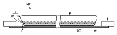
웨이퍼 W는 복수의 점착층(1)을 개재해서 보강용 지지판(2)이 접합되어 있다. 이 웨이퍼 W는 이면 연삭 후의 이면 및 표면에 땜납 볼이나 범프 등의 돌기 전극(3)이 형성되어 있다. 예를 들어, 웨이퍼 W의 두께는 100㎛ 이하이고, 돌기 전극(3)의 두께 및 돌기 전극끼리의 피치가 100㎛이다.The reinforcing supporting
점착층(1)은, 예를 들어 레이저나 가열에 의해 접착력을 감멸하는 분리층(1A)과, 당해 분리층(1A)에 도포된 액상의 점착제층(1B)으로 구성되어 있다. 당해 점착제층(1B)은, 예를 들어 자외선 경화형이며, 웨이퍼 W를 부착한 후에 경화된다. 따라서, 점착제층(1B)은, 웨이퍼 W를 부착한 시점에서는 미경화 상태에 있으므로, 표면에 형성된 돌기 전극끼리의 사이에 점착제가 파고 들어가 밀착하면서도, 웨이퍼 W의 외주로부터 비어져 나와 있다.The
지지판(2)은 웨이퍼 W의 외형보다 큰 유리나 석영으로 구성되어 있다.The
<반도체 웨이퍼의 마운트 장치>≪ Mounting Device of Semiconductor Wafer &
도 3에 본 발명에 따른 반도체 웨이퍼의 마운트 장치의 평면도가 도시되어 있다.3 is a plan view of a mounting apparatus for a semiconductor wafer according to the present invention.
이 마운트 장치는 시트 공급부(5), 점착 테이프 공급부(6), 세퍼레이터 박리 기구(7), 프레임 얼라인먼트부(8), 프레임 반송 기구(9), 마운트 프레임 작성부(10), 웨이퍼 공급부(11), 웨이퍼 반송 기구(12), 웨이퍼 얼라인먼트부(13) 및 프레임 회수부(14)로 구성되어 있다. 이하, 각 구성에 대해서 상세히 설명한다.The mounting apparatus includes a
시트 공급부(5)는 도 4에 도시한 바와 같이, 시트 공급 기구(16), 시트 절단 기구(17), 댄서 롤러(18), 불필요 시트 회수 기구(19), 시트 박리 기구(20) 및 세퍼레이터 회수 기구(21) 등으로 구성되어 있다.4, the
시트 공급 기구(16)는 접착 시트 T를 롤 권취한 원단 롤을 장착하는 보빈을 구비하고 있다. 이 시트 공급 기구(16)는, 원단 롤로부터 조출된 접착 시트 T를, 댄서 롤러(18)를 개재해서 소정의 반송 경로로 유도한다. 또한, 시트 절단 기구(16)는 접착 시트 T를 시트 절단 기구(17)를 거쳐서 시트 박리 기구(20)에 공급하도록 구성되어 있다.The
접착 시트 T는 표면 및 이면에 세퍼레이터 S가 추가 설치되어 있다. 이 접착 시트 T는 다이싱 처리에 의해 웨이퍼 W로부터 분단된 칩의 돌기 전극(3)의 형성면과 실장 기판 사이를 밀봉하는 수지를 포함해서 이루어지는 접착 시트이다. 접착 시트 T는, 예를 들어 접착 및 절연 기능을 갖는 언더필 시트로서의 NCF(Non Conductive Film)나 도전성의 기능을 구비한 ACF(Anisotropic Conductive Film) 등을 들 수 있다.The adhesive sheet T is further provided with a separator S on the front and back surfaces thereof. The adhesive sheet T is an adhesive sheet comprising a resin that seals between the surface of the chip separated from the wafer W by the dicing process and the mounting substrate. The adhesive sheet T may be, for example, an NCF (Non Conductive Film) or an ACF (Anisotropic Conductive Film) having a conductive function as an underfill sheet having an adhesive function and an insulating function.
시트 절단 기구(17)는, 동조 구동하는 절단 롤러(23)와 받침 롤러(24)를 상하로 대향 배치하고 있다. 절단 롤러(23)는, 도 5에 도시한 바와 같이, 절단날(25)을 형성한 시트(26)를 구동 롤러(27)에 장착하여 구성되어 있다. 절단날(25)은 접착 시트 T를 원형으로 절단하는 환상으로 형성되어 있다.The
받침 롤러(24)는 금속제의 구동 롤러이다. 또한, 절단 롤러(23) 또는 받침 롤러(24) 중 적어도 한쪽이 구동 실린더에 의해 승강 가능하게 구성되어 있다. 따라서, 양 롤러(23, 24)의 간극이, 접착 시트 T의 두께에 따라서 설정을 변경 가능하게 한다.The supporting
불필요 시트 회수부(19)는 이면측의 세퍼레이터 S 위에서 원형의 접착 시트편 CT로 잘라 내어져 이어진 불필요한 접착 시트 T'를, 시트 이송 롤러(28)의 직후에 세퍼레이터 S로부터 박리하여 회수 보빈(29)으로 권취하도록 구성되어 있다. 따라서, 접착 시트편 CT가 남겨진 세퍼레이터 S가, 시트 박리 기구(20)로 유도된다.The unnecessary
시트 박리 기구(20)는 도 4에 도시한 바와 같이, 박리 부재(31) 및 흡착 반송 기구(32)로 구성되어 있다.As shown in Fig. 4, the
박리 부재(31)는 접착 시트편 CT를 수평하게 보유 지지 가능한 편평면을 갖는다. 또한, 박리 부재(31)의 선단은, 끝이 가는 테이퍼를 갖고, 당해 선단에서 세퍼레이터 S를 되접어서 세퍼레이터 회수 기구(21)로 안내한다.The peeling
흡착 반송 기구(32)는 접착 시트편 CT의 직경 이상의 크기를 갖는 시트 흡착 테이블(33)을 구비하고 있다. 시트 흡착 테이블(33)은 승강 및 전후 좌우로 수평 이동하도록 구성되어 있다. 즉, 박리 부재(31)의 상방의 대기 위치와 박리 부재(31) 위에서 접착 시트편 CT를 흡착하는 위치 및 접착 시트편 CT를 흡착 후에 접착 시트 T의 이송에 동조하여 그 반송 방향으로 수평 이동한다. 또한, 시트 흡착 테이블(33)은, 접착 시트편 CT를 흡착하여 점착 테이프 공급부(6)측의 지지용 점착 테이프 DT와의 부착 위치로 이동하고, 당해 부착 위치에서도 승강 이동한다. 또한, 시트 흡착 테이블(33)은 본 발명의 시트 보유 지지 기구에 상당한다.The
점착 테이프 공급부(6)는 도 2에 도시한 바와 같이, 프레임 공급부(35), 프레임 반송 기구(36) 및 테이프 부착 기구(37)를 구비하고 있다.As shown in Fig. 2, the adhesive
프레임 공급부(35)는 링 프레임 f를 적층 수납한 웨건 타입의 반송차가 장치 내의 스페이스에 연결되어 구성되어 있다. 반송차는, 그 내부에 승강대가 구비되어 있다. 당해 승강대에 링 프레임 f가 적층되어 있다. 따라서, 승강대는 소정 피치로 상승하면서, 상방의 개구로부터 1매씩 링 프레임 f를 프레임 반송 기구(36)에 전달한다.The
프레임 반송 기구(36)는 가동대(39), 흡착부(40) 및 얼라이너로 구성되어 있다. 가동대(39)는 안내 레일(38)을 따라 프레임 공급부(35)와 점착 테이프 DT의 부착 위치로 나누어서 왕복 이동한다. 가동대(39)는 아암, 흡착부(40) 및 얼라이너 등 구성되어 있다. 아암은 가동대(39)에 세워 설치 고정된 세로 레일을 따라 승강한다. 도 6에 도시한 바와 같이, 당해 아암의 선단측에 흡착부(40)와 얼라이너가 장착되어 있다.The
흡착부(40)는 환상의 플레이트이다. 이 흡착부(40)의 하면에 탄성체를 개재해서 하향의 가압된 복수개의 흡착 패드를 구비하고 있다. 즉, 링 프레임 f는 당해 흡착 패드에 의해 흡착됨과 함께, 표면 전체를 흡착부(40)에 의해 평면 보유 지지되어 있다. 또한, 흡착 패드는, 크기가 다른 링 프레임 f를 흡착 보유 지지 가능하게 배치되어 있다. 즉, 흡착부(40)는 점착 테이프 DT를 부착할 때의 프레임 보유 지지 기구로서 기능한다.The
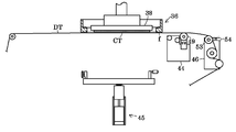
얼라이너는 프레임 f의 직경 방향으로 슬라이드 조정 가능하게 하향으로 세워 설치된 위치 결정용 걸림 결합 핀으로 구성되어 있다.The aligner is constituted by a positioning engagement pin provided so as to be slidably downwardly slidable in the radial direction of the frame f.
테이프 부착 기구(37)는 도 6, 도 15 및 도 16에 도시한 바와 같이, 테이프 공급부(41), 세퍼레이터 회수부(42), 인장 기구(43), 부착 유닛(44), 테이프 절단 기구(45), 박리 유닛(46) 및 테이프 회수부(46)로 구성되어 있다. 이 테이프 부착 기구(37)는 본 발명의 제1 부착 기구에 상당한다.6, 15, and 16, the
테이프 공급부(41)는 지지용 점착 테이프 DT의 원단 롤이 보빈에 장전되어 있다. 이 테이프 공급부(41)로부터 조출된 점착 테이프 DT는 핀치 롤러(47)로 유도된다. 핀치 롤러(47)에 의해 세퍼레이터 S가 박리되어 하방으로 반전 안내된다. 또한, 세퍼레이터 S의 박리에 의해 점착면을 상향으로 노출되는 점착 테이프 DT가 수평하게 인출된다. 그 후, 점착 테이프 DT는 부착 유닛(44)을 거쳐서 박리 유닛(46)으로 유도된다.In the
세퍼레이터 회수부(42)는 테이프 공급부(41)에 의한 점착 테이프 DT의 조출 속도에 동조하여 세퍼레이터 S를 권취 회수한다.The
인장 기구(43)는 도 15 및 도 16에 도시한 바와 같이, 점착 테이프 DT를 사이에 물고 있는 한 쌍의 파지 기구(97A, 97B)를 포함하여 이루어진다.As shown in Figs. 15 and 16, the
파지 기구(97A, 97B)는 고정 받침편(98), 실린더(99) 및 가동편(100)으로 구성되어 있다. 가동편(100)은 실린더(99)에 의해 승강한다. 따라서, 가동편(100)과 고정 받침편은, 개폐할 수 있도록 구성되어 있다. 또한, 파지 기구(97A, 97B)는 장치 프레임에 장착된 지지 프레임(101)에 실린더(102)를 개재해서 장착되어 있다. 즉, 파지 기구(97A, 97B)는 실린더(102)의 신축 동작에 수반하여 파지하고 있는 점착 테이프 T를 폭 방향으로 인장하여 텐션을 부여할 수 있도록 구성되어 있다.The
부착 유닛(44)은 도시되지 않은 나사 이송식 또는 벨트식 등의 구동 기구에 의해 수평으로 왕복 이동 가능하게 구성되어 있다. 또한, 도 6에 도시한 바와 같이, 실린더 등에 의해 승강 가능한 부착 롤러(48) 등이 구비되어 있다.The attaching
테이프 절단 기구(45)는 에어 실린더(50)에 의해 승강됨과 함께, 중심선 Z를 중심으로 해서 선회 구동되는 복수개의 지지 아암(51A, 51B)이 연장되어 있다. 1개의 지지 아암(51A)의 선단에는, 수평축 지지한 커터 브래킷을 개재해서 상하 이동 가능한 원판형 커터(52)가 장착되어 있다. 다른 지지 아암(51B)의 선단에는, 가압 롤러 R이 요동 아암을 개재해서 상하 이동 가능하게 장착되어 있다.The
박리 유닛(46)은 도시되지 않은 나사 이송식 또는 벨트식 등의 구동 기구에 의해 수평하게 왕복 이동 가능하게 구성되어 있다. 또한, 박리 유닛(46)은 박리 롤러(53) 및 푸셔(54) 등을 구비하고 있다. 박리 롤러(53)는 부착 유닛(43)으로부터 수평하게 도출되어 온 점착 테이프 DT를 안내한다. 푸셔(54)는 박리 롤러(53)와 협동하여 점착 테이프 DT를 파지한다.The peeling
테이프 회수부(47)는 박리 유닛(46)의 작동에 동조하여, 테이프 절단 기구(45)에 의해 원형으로 잘라내진 불필요한 점착 테이프 DT'를 보빈에 권취 회수한다.The
세퍼레이터 박리 기구(7)는 테이프 공급부(56), 박리 테이블(57), 박리 롤러(58) 및 테이프 회수부(59)로 구성되어 있다. 이 세퍼레이터 박리 기구(7)는 본 발명의 박리 기구에 상당한다.The
테이프 공급부(56)는 접착 시트 T의 직경보다 폭이 좁은 박리 테이프 PE의 원단 롤이 보빈에 장전되어 있다. 이 테이프 공급부(56)로부터 조출된 박리 테이프 PE는 박리 롤러(58)로 유도된다.The
박리 테이블(57)은 링 프레임 f를 흡착하여 평면 보유 지지하는 플레이트 형상이다. 이 박리 테이블(57)은 접착 시트편 CT의 박리 위치를 기점으로 점착 테이프 DT의 부착 위치 및 프레임 얼라인먼트부(8)로의 전달 위치를 왕복한다.The peeling table 57 is in the shape of a plate which holds and holds the ring frame f by suction. The peeling table 57 reciprocates between the attachment position of the adhesive tape DT and the delivery position to the
박리 롤러(58)는 에어 실린더(60)에 의해 승강 가능하게 구성되어 있다. 즉, 점착 테이프 DT에 접착 시트편 CT가 부착된 링 프레임 f를 흡착하고 있는 박리 테이블(57) 위에서, 접착 시트편 CT의 표면에 추가 설치되어 있는 세퍼레이터 S에 박리 테이프 PE를 부착한다.The peeling
테이프 회수부(59)는 테이프 공급부(56)에 의한 박리 테이프 PE의 조출 및 세퍼레이터 S의 박리 속도에 동조하여 세퍼레이터 S가 부착한 박리 테이프 PE를 권취 회수한다.The
프레임 얼라인먼트부(8)는 반전 아암(61), 얼라인먼트 스테이지(62) 및 광학 센서(63)로 구성되어 있다.The
반전 아암(61)은 지지축 둘레에 요동하도록 아암의 선단에 환상의 흡착 플레이트를 구비하고 있다. 즉, 반전 아암(61)은 박리 테이프(57) 위의 링 프레임 f의 외주측을 흡착하여 반전한 후, 얼라인먼트 스테이지(62) 위에서 링 프레임 f를 보유 지지한 채 수평 보유 지지된다.The reversing
얼라인먼트 스테이지(62)는 반전 아암(61)의 흡착 플레이트와 마찬가지로 환상이며, 링 프레임 f의 외주측을 보유 지지한다. 이때, 접착 시트편 CT가 부착되어 있는 면을 하향으로 해서 링 프레임 f를 보유 지지하고 있다.The
광학 센서(63)는 본 실시예에서는 촬상 장치이다. 2대의 광학 센서(63)에 의해 링 프레임 f와 접착 시트편 CT를 각각 촬상하고, 취득한 화상 데이터를 제어부(64)로 보낸다. 제어부(64)는 링 프레임 f의 내경의 윤곽 화상 및 접착 시트편 CT의 윤곽 화상의 미리 정한 기준 화상과 패턴 매칭하고, 당해 기준 화상과의 어긋남양을 산출한다.The
도 3에 도시하는 프레임 반송 기구(9)는 복수개의 흡착 패드로 링 프레임 f를 흡착 보유 지지하도록 구성되어 있다.The
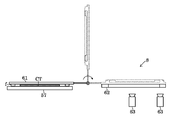
마운트 프레임 작성부(10)는 도 7에 도시한 바와 같이, 챔버(65), 웨이퍼 보유 지지 테이블(66) 및 프레임 보유 지지 테이블(67)로 구성되어 있다. 이 마운트 프레임 작성부(10)를 구성하는 기구는 본 발명의 마운트 기구로서 기능한다.The mount
챔버(65)는 링 프레임 f의 내경보다 작은 외형을 갖는 상하 한 쌍의 하부 하우징(65A)과 상부 하우징(65B)으로 구성되어 있다.The
하부 하우징(65A) 내에는, 승강 가능한 웨이퍼 보유 지지 테이블(66)이 구비되어 있다. 웨이퍼 보유 지지 테이블(66)은 지지판을 갖는 웨이퍼 W를 흡착하는 흡착 블록을 갖고, 하부 하우징(65A)을 관통하는 로드(68)와 연결되어 있다. 로드(68)의 타단부는, 모터 등으로 이루어지는 액추에이터(69)에 구동 연결되어 있다. 따라서, 웨이퍼 보유 지지 테이블(66)은 하부 하우징(65A) 내에서 승강한다.In the
상부 하우징(65B)은 승강 구동 기구(70)에 구비되어 있다. 이 승강 구동 기구(70)는 가동대(73), 가동 프레임(74) 및 아암(75)을 구비하고 있다. 가동대(73)는 세로벽(71)의 배면부에 세로 방향으로 배치된 레일(72)을 따라 승강한다. 가동 프레임(74)은 가동대(73)에 높이 조절 가능하게 지지되어 있다. 아암은 가동 프레임(74)으로부터 전방을 향해서 연장되어 있다. 이 아암(75)의 선단부로부터 하방으로 연장되는 지지축(76)에 상부 하우징(65B)이 장착되어 있다. 가동대(73)는 나사축(77)을 모터(78)에 의해 정역전함으로써, 나사 이송 승강된다.The
상하부 하우징(65A, 65B)에는, 도 8에 도시한 바와 같이, 유로(80)를 통해서 진공 장치(81)와 연통 접속되어 있다. 또한, 상부 하우징(65B)측 유로(80)에는 전자 밸브(82)를 구비하고 있다. 또한, 각 하우징(65A, 65B)에는 대기 개방용 전자 밸브(83, 84)를 구비한 유로(85)가 각각 연통 접속되어 있다. 또한, 상부 하우징(65B)에는 일단 감압한 내압을 누설에 의해 조정하는 전자 밸브(86)를 구비한 유로(87)가 연통 접속되어 있다. 또한, 이들 전자 밸브(82, 83, 84, 86)의 개폐 조작 및 진공 장치(81)의 작동은 제어부(90)에 의해 행해지고 있다.As shown in Fig. 8, the upper and
프레임 보유 지지 테이블(67)은 하부 하우징(65A)의 외주를 둘러싸는 환상이다. 프레임 보유 지지 테이블(67)에 링 프레임 f를 적재했을 때, 하부 하우징(65A)의 접합면과 링 프레임 f의 상면이 같은 평면이 되도록 높이가 설정되어 있다.The frame holding table 67 is an annular shape surrounding the outer periphery of the
도 3으로 되돌아가서, 웨이퍼 공급부(11)에는 카세트 C1이 적재된다. 카세트 C1에는, 다수매의 웨이퍼 W가 수평 자세로 다단으로 삽입 수납되어 있다.Returning to Fig. 3, the cassette C1 is loaded on the
웨이퍼 반송 기구(12)는 로봇 아암(91)을 구비하고 있다. 로봇 아암(91)은 수평하게 진퇴 이동 가능하게 구성됨과 함께, 전체가 선회 및 승강 가능하게 되어 있다. 그리고, 로봇 아암(91)의 선단에는, 말굽형을 한 진공 흡착식의 웨이퍼 보유 지지부가 구비되어 있다. 웨이퍼 보유 지지부는, 카세트 C1에 다단으로 수납된 웨이퍼 W끼리의 간극 속으로 들어가, 웨이퍼 W를 지지면측으로부터 흡착 보유 지지한다. 흡착 보유 지지한 웨이퍼 W는 카세트 C1로부터 인출되어, 웨이퍼 얼라인먼트부(13)의 얼라인먼트 스테이지(93), 웨이퍼 보유 지지 테이블(66)의 순으로 반송된다.The
웨이퍼 얼라인먼트부(13)는 얼라인먼트 스테이지(93)를 갖는다. 따라서, 웨이퍼 반송 기구(12)에 의해 얼라인먼트 스테이지(93)에 적재된 웨이퍼 W의 외주로부터 노치나 오리엔테이션 플랫을 검출하고, 당해 검출 결과에 기초하여 위치 정렬을 행한다.The
프레임 회수부(14)에는 카세트 C2가 적재된다. 카세트 C2에는 작성된 마운트 프레임 MF가 지지판(2)의 표면을 하향으로 한 수평 자세로 다단으로 삽입 수납되어 있다.The cassette C2 is loaded on the
본 발명에 따른 반도체 웨이퍼의 마운트 장치는 이상과 같이 구성되어 있다. 당해 마운트 장치를 사용해서 접착 시트편 CT를 점착 테이프 DT에 부착한 후의 링 프레임 f에, 웨이퍼 W를 마운트하는 일순의 동작을, 도 9에 나타내는 플로우차트 및 도 10 내지 도 27을 참조하면서 설명한다.The mounting apparatus for a semiconductor wafer according to the present invention is configured as described above. The operation of mounting the wafer W on the ring frame f after attaching the adhesive sheet piece CT to the adhesive tape DT using the mount device will be described with reference to the flowchart shown in Fig. 9 and Figs. 10 to 27 .
마운트 장치를 작동하면, 웨이퍼 공급 라인, 시트 공급 라인 및 점착 테이프 공급 라인이 동시에 병렬 처리를 개시한다.When the mount device is operated, the wafer supply line, the sheet supply line, and the adhesive tape supply line simultaneously start the parallel processing.
우선, 웨이퍼 공급 라인에 대해서 설명한다. 로봇 아암(91)의 선단에서 지지판(2)을 흡착하고, 카세트 C1로부터 웨이퍼 W를 반출한다(스텝 S1A). 로봇 아암(91)은 얼라인먼트 스테이지(93)의 보유 지지면으로부터 돌출되어 있는 흡착 패드에 전달한다. 얼라인먼트 스테이지(93)는 흡착 패드에 의해 지지판(2)을 흡착한 채 웨이퍼 W에 형성된 노치 등의 위치 결정 부위에 기초하여 중심 위치를 구하여 위치 정렬한다(스텝 S2A). 위치 정렬이 완료되면, 흡착 패드에 의해, 흡착면으로부터 들어 올려진 웨이퍼 W는 다시 로봇 아암(91)에 의해 흡착되어, 하부 하우징(65A) 측으로 반송된다.First, the wafer supply line will be described. The
웨이퍼 보유 지지 테이블(66)은, 도 10에 도시한 바와 같이, 하부 하우징(65A)의 정상부(접합부)보다 높게 복수개의 지지 핀(95)을 밀어 올려서 지지판(2)을 하향으로 한 웨이퍼 W를 수취한다. 웨이퍼 W를 수취한 지지 핀(95)은 하강한다. 웨이퍼 보유 지지 테이블(66)은 보유 지지면에서 웨이퍼 W를 흡착 보유 지지한다(스텝 S3A). 이때, 웨이퍼 W의 돌기 전극(3)이 형성된 이면은, 하부 하우징(65A)의 접합부보다 낮은 위치에 있다. 또한, 후술하는 얼라인먼트 데이터에 기초하여, 부착 대상의 접착 시트편 CT의 중심과 웨이퍼 W의 중심이 일치하도록 웨이퍼 보유 지지 테이블(66)에 적재된다.10, the wafer holding table 66 pushes up the plurality of support pins 95 higher than the top (joining portion) of the
시트 공급 라인에서는, 다음 처리가 행해진다. 테이프 공급 기구(16)는 띠 형상의 접착 시트 T를 조출 공급한다(스텝 S1B). 세퍼레이터 S를 갖는 접착 시트 T는 시트 절단 기구(17)의 절단 롤러(23)와 받침 롤러(24) 사이를 통과하는 과정에서, 회전 구동하는 절단 롤러(23)에 의해 세퍼레이터 S 위에서 원형 접착 시트편 CT에 하프컷되어 간다(스텝 S2B).In the sheet feed line, the following process is performed. The
하프컷이 끝난 접착 시트 T는, 댄서 롤러(18)를 경유해서 불필요 시트 회수부(19)로 보내진다. 이 과정에서 불필요 시트 회수부(19)는 접착 시트편 CT를 잘라낸 후의 불필요한 접착 시트 CT'를 시트 이송 롤러(28)에 의해 박리하고, 회수 보빈(29)에 권취 회수해 간다(스텝 S3B).The half-cut adhesive sheet T is sent to the unnecessary
접착 시트편 CT가 남겨진 이면측의 세퍼레이터 S는 시트 박리 기구(20)로 보내진다. 시트 박리 기구(20)는 접착 시트편 CT가 박리 위치에 도달하면, 댄서 롤러(18)에 의한 접착 시트 T의 인입 작동에 의해, 도 11에 도시한 바와 같이, 접착 시트편 CT를 박리 부재(31) 위에서 정지시킨다. 도 12에 도시한 바와 같이, 동시에 흡착 반송 기구(32)의 시트 흡착 테이블(33)을 하강시켜서 접착 시트편 CT에 접촉시켜서 흡착을 개시한다.The separator S on the back side where the adhesive sheet piece CT is left is sent to the
시트 흡착 테이블(33)이 접착 시트편 CT를 흡착하면, 댄서 롤러(18)를 조작하여 접착 시트 T의 이송을 재개시킨다. 이때, 도 13에 도시한 바와 같이, 접착 시트 T의 이송 속도에 동조시켜서 시트 흡착 테이블(33)을 시트 반송 방향으로 이동시킨다.When the sheet adsorption table 33 adsorbs the adhesive sheet piece CT, the conveyance of the adhesive sheet T is restarted by operating the
시트 흡착 테이블(33)은 박리 부재(31)에 의해 세퍼레이터 S가 박리된 접착 시트편 CT만을 흡착 보유 지지한다(스텝 S4B). 동시에 세퍼레이터 회수 기구(21)는 세퍼레이터 S를 보빈에 권취 회수해 간다(스텝 S5B).The sheet adsorption table 33 adsorbs and holds only the adhesive sheet pieces CT from which the separator S has been peeled off by the peeling member 31 (step S4B). At the same time, the separator recovery mechanism 21 winds the separator S on the bobbin and collects it (step S5B).
시트 흡착 테이블(33)은 접착 시트편 CT를 보유 지지한 채 상승하고, 점착 테이프 공급 라인측의 부착 위치의 상방으로 이동한다(스텝 S6B).The sheet suction table 33 ascends holding the adhesive sheet piece CT, and moves upward above the attachment position on the adhesive tape supply line side (step S6B).
점착 테이프 공급 라인에서는, 다음 처리가 행해진다. 프레임 반송 기구(36)가 프레임 공급부(35)로부터 링 프레임 f를 흡착하여 취출한다(스텝 S1C). 프레임 반송 기구(36)는 링 프레임 f를 흡착 보유 지지한 채 당해 링 프레임 f의 얼라인먼트를 행한 후에(스텝 S2C), 도 14에 도시한 바와 같이, 당해 링 프레임 f를 테이프 부착 위치까지 반송한다. 도 14 내지 도 16에 도시한 바와 같이, 인장 기구(43)에 의해 점착 테이프 DT의 폭 방향으로 텐션을 부여하여 연신한다. 동시에, 점착 테이프 DT의 공급과 권취 동작에 의해 길이 방향으로 소정의 텐션을 부여하고, 박리 롤러(53)와 푸셔(54)의 조 및 핀치 롤러(47)에 의해 점착 테이프 DT를 해당 상태에서 보유 지지한다(스텝 S3C). 이때, 점착 테이프 DT에 부여하는 텐션은, 점착 테이프 DT의 소성 변형에 이르지 않도록 설정되어 있다.In the adhesive tape supply line, the following processing is performed. The
점착 테이프 DT로의 텐션의 부여가 완료되면, 부착 유닛(44)을 작동시킨다. 즉, 도 17에 도시한 바와 같이, 부착 롤러(49)가 상승하여 점착 테이프 DT를 가압하면서, 링 프레임 f에 점착 테이프 DT를 부착해 간다(스텝 S4C).When the application of the tension to the adhesive tape DT is completed, the attaching
이어서, 도 18에 도시한 바와 같이, 링 프레임 f의 개구부를 향해서 흡착 반송 기구(32)의 시트 흡착 테이블(33)에 의해 흡착되어 있는 접착 시트편 CT를 하강시켜, 점착 테이프 DT와 접착 시트편 CT를 근접 대향시키도록 위치 및 높이를 조정한다(스텝 S7).18, the adhesive sheet piece CT attracted by the sheet suction table 33 of the
위치 정렬이 완료되면, 도 19에 도시한 바와 같이, 부착 유닛(44)의 부착 롤러(49)를 상승시킨 채, 대기 위치측으로 이동시키는 과정에서, 점착 테이프 DT를 가압하면서 접착 시트편 CT에 부착해 간다(스텝 S8).19, in the course of moving the attaching
점착 테이프 DT의 부착이 완료되면, 도 20에 도시한 바와 같이, 테이프 절단 기구(45)는 커터(52)를 상승시켜서 점착 테이프 DT에 가압한다. 그 상태 그대로 커터(52)를 선회시키면서 링 프레임 f의 형상으로 당해 점착 테이프 DT를 절단함과 함께, 당해 커터(52)의 이동에 추종하여 절단된 점착 테이프 DT의 부위를 가압 롤러 R이 전동하여 뜰뜨는 부분을 부착한다. 점착 테이프 DT의 절단이 완료되면, 테이프 절단 기구(45)는 커터(52)를 하방의 대기 위치로 되돌린다.When the attachment of the adhesive tape DT is completed, as shown in Fig. 20, the
그 후, 박리 유닛(46)은 푸셔(54)를 해제하고, 도 21에 도시한 바와 같이, 부착 유닛(44)의 초기 위치로 이동하면서 절단 후의 점착 테이프 DT를 링 프레임 f로부터 박리해 간다(스텝 S9).Thereafter, the peeling
불필요한 점착 테이프 DT'의 박리가 완료되면, 박리 유닛(46)이 초기 위치로 되돌아감과 함께, 도 22에 도시한 바와 같이, 흡착 반송 기구(32) 및 프레임 반송 기구(36)가 소정의 높이까지 상승하여 정지한다.When the peeling of the unnecessary adhesive tape DT 'is completed, the peeling
이들 흡착 반송 기구(32) 및 프레임 반송 기구(36)와 점착 테이프 DT 사이에 박리 테이블(57)이 진입하여 소정 위치에서 정지한다. 그 후, 흡착 반송 기구(32) 및 프레임 반송 기구(36)를 하강시켜서, 도 23에 도시한 바와 같이, 점착 테이프 DT 및 접착 시트편 CT를 갖는 링 프레임 f를 박리 테이블(57)에 전달한다. 박리 테이블(57)은 링 프레임 f를 흡착한 채 세퍼레이터 박리 기구(7)의 박리 위치까지 이동한다.The peeling table 57 enters between the
박리 롤러(58)가 접착 시트편 CT의 일단부측으로 하강하고, 도 24에 도시한 바와 같이, 박리 테이프 PE를 부착한다. 그 후, 도 25에 도시한 바와 같이, 박리 테이블(57)을 이동시킴과 함께, 이동 속도에 동조시켜서 테이프 공급부(56)로부터 박리 테이프 PE를 공급하면서, 테이프 회수부(59)에 의해 박리 테이프 PE와 일체가 된 세퍼레이터 S를 권취 회수한다(스텝 S9).The peeling
접착 시트편 CT로부터 세퍼레이터 S의 박리가 완료되면, 박리 테이블(57)은 도 26에 도시한 바와 같이, 프레임 얼라인먼트부(8)로 이동한다. 반전 아암(61)이 박리 테이블(57) 위의 링 프레임 f를 흡착 보유 지지하면 반전하고, 프레임 얼라인먼트부(8)의 얼라인먼트 스테이지(62)에 수평 보유 지지된다(스텝 S10).When peeling of the separator S from the adhesive sheet piece CT is completed, the peeling table 57 is moved to the
프레임 얼라인먼트부(8)는 링 프레임 f측으로부터 2대의 촬상 장치(63)에서 링 프레임 f와 접착 시트편 CT를 촬상한다. 제어부(64)가 취득한 실제 화상 데이터와 기준 화상 데이터로부터 양 화상의 패턴 매칭을 행하고, 링 프레임 f의 중심 좌표와 접착 시트편 CT의 중심 좌표의 어긋남양을 구한다(스텝 S11). 구한 어긋남양에 기초하여, 로봇 아암(91)을 조작하여, 웨이퍼 보유 지지 테이블(66) 위에서 웨이퍼 W의 중심 위치가 접착 시트편 CT의 중심 위치와 일치하도록, 당해 웨이퍼 보유 지지 테이블(66) 위에 웨이퍼 W를 적재한다.The
얼라인먼트 데이터의 취득이 완료되면, 프레임 반송 기구(9)가 링 프레임 f를 흡착 보유 지지하여 프레임 보유 지지 테이블(67)로 반송한다(스텝 S12).When the acquisition of the alignment data is completed, the
웨이퍼 보유 지지 테이블(66)과 프레임 보유 지지 테이블(67) 각각에 웨이퍼 W와 링 프레임 f가 적재되면, 도 27에 도시한 바와 같이, 상부 하우징(65B)을 하강시키고, 하부 하우징(65A)으로 점착 테이프 DT를 물어서 챔버(65)를 형성한다.When the wafer W and the ring frame f are loaded on the wafer holding table 66 and the frame holding table 67 respectively, the
제어부(90)는 전자 밸브(83, 84, 86)를 닫은 상태에서, 진공 장치(81)를 작동시켜서 상부 하우징(65B) 내와 하부 하우징(65A) 내를 감압한다. 이때, 양 하우징(65A, 65B) 내가 동일한 속도로 감압해 가도록, 전자 밸브(82)의 개방도를 조정한다.The
양 하우징(65A, 65B) 내가 소정의 기압까지 감압되면, 제어부(90)는 전자 밸브(82)를 닫음과 함께, 진공 장치(81)의 작동을 정지한다.When the both
제어부(90)는 전자 밸브(86)의 개방도를 조정하여 누설시키면서 상부 하우징(65B) 내를 소정의 기압까지 서서히 높인다. 이때, 하부 하우징(65A) 내의 기압이 상부 하우징(65B) 내의 기압보다 낮아져서 그 차압에 의해, 점착 테이프가 중심으로부터 하부 하우징(65A) 내로 인입되어 간다. 즉, 점착 테이프 DT와 접착 시트편 CT가, 도 28에 도시한 바와 같이, 웨이퍼 W를 향해서 오목하게 만곡하고, 근접 배치된 웨이퍼 W의 중심으로부터 외주를 향해서 서서히 부착되어 간다. 이때, 점착 테이프 DT가 오목하게 만곡되는 데 수반하여, 접착 시트편 CT가 웨이퍼 형상까지 방사상으로 연신되어, 웨이퍼 W의 이면 전체에 부착된다.The
미리 설정된 기압에 상부 하우징(65B) 내가 도달하면, 제어부(90)는 전자 밸브(84)의 개방도를 조정하여 하부 하우징(65A) 내의 기압을 상부 하우징(65B) 내의 기압과 동일하게 한다. 이 기압 조정에 따라서 웨이퍼 보유 지지 테이블(66)을 상승시켜서 하부 하우징(65A)의 접합부와 점착 테이프 DT의 이면을 동일한 높이로 한다.When the
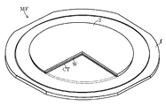
제어부(90)는 상부 하우징(65B)을 상승시켜서 상부 하우징(65B) 내를 대기 개방함과 함께, 전자 밸브(84)를 완전 개방으로 하여 하부 하우징(65A) 측도 대기 개방한다. 이 시점에서, 마운트 프레임 MF가 작성되어 있다(스텝 S13). 즉, 도 29 및 도 30에 도시한 바와 같이, 웨이퍼 W의 외형으로부터 접착 시트편 CT가 비어져 나오지 않고 점착 테이프 DT와 웨이퍼 W 사이에 부착되어 있다.The
작성된 마운트 프레임 MF를 반송 기구(96)로 반출하여 반전하고, 지지판(2)을 상측으로 하여 카세트 C2에 수납한다(스텝 S14).The prepared mount frame MF is carried out by the
이상으로 일련의 처리가 완료되고, 소정 매수의 처리가 완료될 때까지 상기 처리가 반복해서 행해진다(스텝 S15).The above process is repeated until a series of processes are completed and a predetermined number of processes are completed (step S15).
상기 실시예 장치에 따르면, 점착 테이프 DT에 접착 시트편 CT를 부착한 후에, 챔버(65) 내에서 차압을 이용해서 당해 접착 시트편 CT를 웨이퍼 W에 부착하고 있다. 따라서, 점착 테이프 DT와 함께 접착 시트편 CT가, 웨이퍼 W를 향해서 오목하게 만곡된다. 즉, 오목하게 만곡된 접착 시트편 CT의 정점이 웨이퍼 W의 중심에 접촉하고, 웨이퍼 W의 이면에 방사상으로 부착되어 간다. 따라서, 웨이퍼 W의 이면에 형성된 돌기 전극간의 공기가 외측으로 배출되면서 접착 시트편 CT가 부착되므로, 접착 계면에 기포의 혼입이 발생하지 않는다.According to the above embodiment apparatus, after the adhesive sheet piece CT is attached to the adhesive tape DT, the adhesive sheet piece CT is attached to the wafer W by using a differential pressure in the
또한, 웨이퍼 W의 외형보다 작게 절단된 접착 시트편 CT를 웨이퍼 W의 이면에 부착하므로, 웨이퍼 W의 외형으로부터 비어져 나와 있는 점착층(1)이나 지지판(2)에 접착 시트 CT가 부착하는 일이 없다. 따라서, 지지판(2)이나 점착층(1)을 박리할 때 발생한 박리 에러를 회피할 수 있다.Further, since the adhesive sheet piece CT cut smaller than the outer shape of the wafer W is attached to the back surface of the wafer W, adhesion of the adhesive sheet CT to the
또한, 접착 시트편 CT를 웨이퍼 W의 이면에 부착할 때 오목하게 만곡시킴으로써, 접착 시트편 CT를 웨이퍼 W의 외형까지 연신할 수 있다. 따라서, 웨이퍼 W의 이면에 접착 시트편 CT의 미 접착 영역이 발생하지 않으므로, 다이싱 처리 시에 웨이퍼 W의 외주 영역의 칩 이면이 물이나 분진으로 오염되는 일이 없으며, 분단된 칩이 비산하는 것을 회피할 수 있다.When the adhesive sheet piece CT is attached to the back surface of the wafer W, the adhesive sheet piece CT can be extended to the outer shape of the wafer W by curving concavely. Therefore, since the unbonded area of the adhesive sheet piece CT does not occur on the back surface of the wafer W, the back surface of the chip of the peripheral region of the wafer W during dicing processing is not contaminated with water or dust, Can be avoided.
또한, 본 발명은 이하와 같은 형태로 실시할 수도 있다.Further, the present invention may be carried out in the following manner.
(1) 상기 실시예에서는, 띠 형상의 접착 시트 T를 하프컷하였지만, 미리 접착 시트편 CT에 프리컷된 원단 롤을 사용해도 된다. 또한, 점착 테이프 DT도 원형 프리컷된 것을 이용해도 된다. 따라서, 띠 형상의 접착 시트 T 및 점착 테이프 DT 또는 프리컷된 접착 시트 T 및 점착 테이프 DT를 각각 조합해서 실시할 수도 있다.(1) In the above embodiment, the strip-shaped adhesive sheet T is half cut, but a raw roll precut in the adhesive sheet piece CT may be used in advance. Further, the adhesive tape DT may be a circular free-cut tape. Therefore, the strip-shaped adhesive sheet T and the adhesive tape DT or the pre-cut adhesive sheet T and the adhesive tape DT can be combined with each other.
또한, 복수매의 접착 시트편 CT를, 소정 피치를 두고 미리 접합한 띠 형상의 점착 테이프 DT를 이용해도 된다. 당해 점착 테이프 DT를 상기 실시예 장치에 이용하는 경우, 다음과 같이 하여 마운트 처리를 행한다.In addition, a strip-shaped adhesive tape DT in which a plurality of sheets of adhesive sheet CT are preliminarily bonded at a predetermined pitch may be used. When the adhesive tape DT is used in the apparatus of the above embodiment, the mounting process is performed as follows.
점착 시트 DT를 테이프 공급부(41)에 세트한다. 링 프레임 f에 점착 테이프 DT를 부착할 때, 점착 테이프 DT에 텐션을 부여하는 것에 수반하여, 접착 시트편 CT에도 텐션이 부여된다. 즉, 링 프레임 f에의 부착 과정에서, 접착 시트편 CT를 웨이퍼 W의 형상까지 연신하여 점착 테이프 DT를 링 프레임 f에 부착할 수 있다.The adhesive sheet DT is set in the
접착 시트편 CT가 추가 설치된 점착 테이프 DT를 부착한 링 프레임 f를 세퍼레이터 박리 기구(7)로 반송하고, 접착 시트편 CT로부터 세퍼레이터 S를 박리한다. 그 후, 상기 실시예와 마찬가지로, 프레임 얼라인먼트부(8)에서의 얼라인먼트 처리된 후에, 마운트 프레임 작성부(10)로 반송된다.The ring frame f provided with the adhesive tape DT provided with the adhesive sheet piece CT is conveyed to the
마운트 프레임 작성부(10)는, 도 31에 도시한 바와 같이, 상부 하우징(65)의 내부에 승강 가능한 플레이트 형상의 부착 부재(105)를 구비하고 있다. 당해 구성에 의해, 링 프레임 f를 프레임 보유 지지 테이블(67)에 적재하면, 상부 하우징(65B)을 하강시켜서 챔버(65)를 형성한다. 그 후, 점착 테이프 DT에서 구획된 양 공간을 동일한 기압으로 감압하면서, 도 32에 도시한 바와 같이, 부착 부재(105)에 의해 점착 테이프 DT를 가압하여 웨이퍼 W에 접착 시트편 CT를 부착한다. 그 후, 챔버(65)를 대기압으로 되돌려서 개방한 후에, 반송 기구(96)로 마운트 프레임 MF를 반출하고, 상방에서 반전시킨 후에 프레임 회수부(14)에 수납한다.As shown in Fig. 31, the mount
이 구성에 따르면, 접착 시트편 CT에 웨이퍼 W를 부착할 때 접착 시트편 CT를 연신시킬 필요가 없으므로, 챔버 내에 기압 컨트롤이 용이해진다.According to this configuration, since it is not necessary to elongate the adhesive sheet piece CT when the wafer W is attached to the adhesive sheet piece CT, control of air pressure in the chamber is facilitated.
또한, 챔버(65) 내에 구비한 부착 부재는, 플레이트에 한정되지 않고 롤러 등이어도 된다.The attachment member provided in the
당해 변형예 장치의 경우, 점착 테이프 DT에 텐션을 부여하여 링 프레임 f에 부착한 후에, 웨이퍼 W와 동일한 크기의 시트 CT를 점착 테이프 DT에 부착하고 나서 당해 접착 시트편 CT를 웨이퍼 W에 부착해도 된다. 웨이퍼 W로의 접착 시트편 CT의 부착은, 챔버(65)를 이용하여 감압 상태에서 부착 부재에 의해 점착 테이프 DT를 가압하여 부착도 되고, 챔버(65)를 개방한 상태에서 부착 부재에 의해 점착 테이프 DT를 가압하여 부착해도 된다.In the case of the modified apparatus, after the adhesive tape DT is attached to the ring frame f, the sheet CT having the same size as the wafer W is attached to the adhesive tape DT and then the adhesive sheet CT is attached to the wafer W do. Attachment of the adhesive sheet piece CT to the wafer W can be carried out by pressing the adhesive tape DT by the attaching member in a reduced pressure state using the
이 구성의 경우, 접착 시트편 CT가 탄성 변형하기 어려운 경우에 적합하다.This configuration is suitable when the adhesive sheet piece CT is difficult to elastically deform.
(2) 상기 실시예에서는, 대기 개방 상태에서 접착 시트편 CT를 웨이퍼 W에 부착해도 된다. 예를 들어, 점착 테이프 DT에 접착 시트편 CT를 부착한 후에, 얼라인먼트 처리에 의해 접착 시트편 CT와 웨이퍼 W의 중심 위치를 일치시켜서 근접 대향 배치한다. 점착 테이프 DT의 이면측으로부터 탄성체로 피복된 롤러를 전동시켜 점착 테이프 DT의 이면측과 함께 접착 시트편 CT를 가압하여 웨이퍼 W의 이면에 부착한다.(2) In the above embodiment, the adhesive sheet piece CT may be attached to the wafer W in the air-releasing state. For example, after the adhesive sheet piece CT is attached to the adhesive tape DT, the adhesive sheet piece CT is aligned with the center position of the wafer W by the alignment process and disposed in close proximity to each other. The roller coated with the elastic material is transferred from the back side of the adhesive tape DT to press the adhesive sheet piece CT together with the back side of the adhesive tape DT to adhere to the back surface of the wafer W.
(3) 상기 실시예에서는, 시트 공급부(5)에 있어서, 하프컷된 접착 시트편 CT의 얼라인먼트 처리를 행하고, 점착 테이프 DT에 부착해도 된다. 예를 들어, 광학 센서의 카메라 등으로 접착 시트편 CT를 촬상하고, 촬상 결과로부터 당해 접착 시트편 CT의 중심 위치를 구하고, 흡착 반송 기구(32)의 중심과 접착 시트편 CT가 일치하도록 흡착 보유 지지하여 부착 위치로 반송한다. 또한, 부착 위치 링 프레임 f의 중심 위치를 마찬가지로 해서 구하고, 링 프레임 f와 중심을 맞추고 나서 점착 테이프 DT를 링 프레임 f와 접착 시트편 CT에 부착한다.(3) In the above embodiment, the half-cut adhesive sheet piece CT may be aligned in the
(4) 상기 변형예 장치에 있어서, 챔버(65) 내에 히터를 배치하고, 접착 시트편 CT를 가열시키면서 웨이퍼 W의 이면에 부착하도록 구성해도 된다. 가열 온도는, 접착 시트편 CT를 적절하게 연화시키는 정도이고, 또한 미경화 상태를 유지할 수 있는 온도이다.(4) In the above modified example, a heater may be disposed in the
(5) 상기 변형예 장치에 있어서, 챔버(65)는 링 프레임 f마다 수납할 수 있도록 구성해도 된다.(5) In the modification example, the
(6) 상기 각 실시예 장치에서는, 하프컷 처리 후에 불필요한 접착 시트 T를 시트 박리 기구(20)로 보내는 도중에 박리하였지만, 시트 박리 기구(20)로 세퍼레이터 S와 함께 권취 회수해도 된다.(6) In each of the above-described embodiments, the adhesive sheet T unnecessary after the half-cut process is peeled off while being sent to the
(7) 상기 실시예 장치에서는, 링 프레임 f에의 점착 테이프 DT의 부착과, 점착 테이프 DT에의 접착 시트편 CT의 부착을 다른 부착 롤러를 이용하여 부착해도 된다. 예를 들어, 링 프레임 f의 점착 테이프 DT의 부착은, 링 프레임 f보다 큰 부착 롤러를 이용하여, 접착 시트편용은 접착 시트편 CT의 직경 이상으로 링 프레임 f의 내경 이하의 크기인 것을 이용한다.(7) In the above embodiment, the attachment of the adhesive tape DT to the ring frame f and the attachment of the adhesive sheet CT to the adhesive tape DT may be attached using different attachment rollers. For example, the adhesive tape DT of the ring frame f is attached using an attachment roller larger than the ring frame f, and the adhesive sheet piece is of a size equal to or smaller than the inner diameter of the ring frame f.
이 구성에 따르면, 링 프레임 f 내에서 부착 롤러를 이동시키므로, 접착 시트편 CT를 가압하기 쉬워지고, 나아가서는 점착 테이프 DT에 접착 시트편 CT를 부착하기 쉬워진다.According to this configuration, since the attachment roller is moved in the ring frame f, the adhesive sheet piece CT is easily pressed, and the adhesive sheet piece CT can be easily attached to the adhesive tape DT.
Claims (9)
상기 점착 테이프를 연신하여 링 프레임에 부착한 후에, 상기 반도체 웨이퍼의 외형 이하의 접착 시트를 당해 반도체 웨이퍼와 당해 점착 테이프 사이에 개재시켜서 반도체 웨이퍼를 점착 테이프에 마운트하는 것을 포함하는 반도체 웨이퍼의 마운트 방법.A semiconductor wafer mounting method for mounting a semiconductor wafer on a pressure sensitive adhesive tape by sandwiching a reinforcing adhesive sheet between a surface of a semiconductor wafer to which a support plate is added and a supporting adhesive tape attached to a ring frame,
Mounting the semiconductor wafer on the adhesive tape by stretching the adhesive tape and attaching the adhesive sheet to the adhesive tape after the adhesive tape is attached to the ring frame and then the adhesive sheet below the outer shape of the semiconductor wafer is sandwiched between the semiconductor wafer and the adhesive tape. .
상기 접착 시트가 반도체 웨이퍼보다 작은 경우, 점착 테이프에 부착한 후, 당해 점착 테이프와 함께 접착 시트를 반도체 웨이퍼와 동일 형상까지 연신하면서 반도체 웨이퍼에 부착하는 반도체 웨이퍼의 마운트 방법.The method according to claim 1,
Wherein when the adhesive sheet is smaller than the semiconductor wafer, the adhesive sheet is adhered to the semiconductor wafer while being stretched to the same shape as the semiconductor wafer together with the adhesive tape.
상기 링 프레임에 부착된 점착 테이프의, 당해 링 프레임과 반도체 웨이퍼 사이의 부분을 한 쌍의 하우징 사이에 끼워 넣고,
양 하우징을 접합하여 형성된 챔버 내에서, 점착 테이프 위의 접착 시트와 반도체 웨이퍼를 근접 대향시켜서 반도체 웨이퍼측의 공간을 다른 쪽 공간보다 기압을 낮게 하면서 접착 시트를 반도체 웨이퍼에 부착하는 반도체 웨이퍼의 마운트 방법.3. The method of claim 2,
A portion of the adhesive tape attached to the ring frame between the ring frame and the semiconductor wafer is sandwiched between the pair of housings,
A mounting method of a semiconductor wafer in which an adhesive sheet on a pressure-sensitive adhesive tape and a semiconductor wafer are placed close to each other in a chamber formed by bonding both housings to adhere the adhesive sheet to a semiconductor wafer while lowering a space on the semiconductor wafer side .
상기 반도체 웨이퍼의 외형보다 작은 접착 시트를 점착 테이프에 부착하는 제1 부착 과정과,
상기 점착 테이프와 함께 접착 시트를 반도체 웨이퍼의 외형까지 연신하여 링 프레임에 부착하는 제2 부착 과정과,
상기 반도체 웨이퍼와 점착 테이프 사이에 접착 시트를 개재시켜서 반도체 웨이퍼를 점착 테이프에 마운트하는 마운트 과정을 포함하는 반도체 웨이퍼의 마운트 방법.A semiconductor wafer mounting method for mounting a semiconductor wafer on a pressure sensitive adhesive tape by sandwiching a reinforcing adhesive sheet between a surface of a semiconductor wafer to which a support plate is added and a supporting adhesive tape attached to a ring frame,
A first attaching step of attaching an adhesive sheet smaller than the outer shape of the semiconductor wafer to the adhesive tape;
A second attaching step of stretching the adhesive sheet to the outer shape of the semiconductor wafer together with the adhesive tape and attaching the adhesive sheet to the ring frame,
And mounting the semiconductor wafer on the adhesive tape with the adhesive sheet interposed between the semiconductor wafer and the adhesive tape.
상기 마운트 과정에서는, 적어도 반도체 웨이퍼를 챔버 내에 수납하고, 감압 상태에서 부착 부재에 의해 점착 테이프를 가압하여 접착 시트를 개재시켜서 당해 반도체 웨이퍼를 점착 테이프에 마운트하는 반도체 웨이퍼의 마운트 방법.5. The method of claim 4,
In the mounting process, at least a semiconductor wafer is housed in a chamber, and the pressure-sensitive adhesive tape is pressed by an attaching member in a reduced pressure state to mount the semiconductor wafer on the adhesive tape with the adhesive sheet interposed therebetween.
상기 반도체 웨이퍼의 외형 이하의 상기 접착 시트를 공급하는 시트 공급 기구;
세퍼레이터를 개재해서 상기 접착 시트를 보유 지지하는 시트 보유 지지 기구;
상기 링 프레임을 보유 지지하는 프레임 보유 지지 기구;
상기 점착 테이프를 공급하는 테이프 공급 기구;
상기 점착 테이프에 텐션을 부여하는 인장 기구;
상기 프레임 보유 지지 기구에 보유 지지된 링 프레임과 시트 보유 지지 기구에 보유 지지된 시트에 상기 인장 기구에 의해 텐션이 부여된 점착 테이프를 부착하는 제1 부착 기구;
상기 접착 시트로부터 세퍼레이터를 박리하는 박리 기구;
상기 반도체 웨이퍼를 보유 지지하는 웨이퍼 보유 지지 테이블;
상기 접착 시트가 추가 설치된 점착 테이프가 부착된 링 프레임을 보유 지지하는 프레임 보유 지지 테이블; 및
상기 접착 시트에 반도체 웨이퍼를 마운트하는 마운트 기구
를 포함하는 반도체 웨이퍼의 마운트 장치.There is provided a semiconductor wafer mounting apparatus for mounting a semiconductor wafer on a pressure-sensitive adhesive tape, with a bonding reinforcing adhesive sheet interposed between a surface of the semiconductor wafer to which the protruding electrodes are provided and a supporting adhesive tape attached to the ring frame,
A sheet supply mechanism for supplying the adhesive sheet below the external shape of the semiconductor wafer;
A sheet holding mechanism for holding the adhesive sheet via a separator;
A frame holding mechanism for holding the ring frame;
A tape supply mechanism for supplying the adhesive tape;
A tensioning mechanism for applying tension to the adhesive tape;
A first attaching mechanism for attaching an adhesive tape to which a tension is applied by the tension mechanism to a ring frame held by the frame holding mechanism and a sheet held by the sheet holding mechanism;
A peeling mechanism for peeling the separator from the adhesive sheet;
A wafer holding table for holding the semiconductor wafer;
A frame holding table for holding a ring frame to which an adhesive tape having the adhesive sheet added thereto is attached; And
A mounting mechanism for mounting a semiconductor wafer on the adhesive sheet;
And a mounting device for mounting the semiconductor wafer.
상기 마운트 기구는,
웨이퍼 보유 지지 테이블을 수납함과 함께, 링 프레임과 반도체 웨이퍼 사이의 점착 테이프를 물고 있는 한 쌍의 하우징을 포함하여 이루어지는 챔버;
상기 점착 테이프에 의해 구획된 챔버 내의 2개의 공간에 차압을 발생시키고, 당해 점착 테이프 및 접착 시트를 오목하게 만곡시키면서 반도체 웨이퍼에 당해 접착 시트를 부착하는 제2 부착 기구를 포함하는 반도체 웨이퍼의 마운트 장치.The method according to claim 6,
The mounting mechanism includes:
A chamber for accommodating the wafer holding table and including a pair of housings for holding an adhesive tape between the ring frame and the semiconductor wafer;
And a second attachment mechanism for generating a differential pressure in two spaces in the chamber partitioned by the adhesive tape and attaching the adhesive sheet to the semiconductor wafer while concavely curving the adhesive tape and the adhesive sheet, .
상기 링 프레임을 보유 지지하는 프레임 보유 지지 기구;
상기 반도체 웨이퍼의 외형 이하의 접착 시트가 미리 부착된 점착 테이프를 공급하는 테이프 공급 기구;
상기 점착 테이프에 텐션을 부여하는 인장 기구;
상기 프레임 보유 지지 기구에 보유 지지된 링 프레임에 상기 인장 기구에 의해 텐션이 부여된 점착 테이프를 부착하는 제1 부착 기구;
상기 접착 시트로부터 세퍼레이터를 박리하는 박리 기구;
상기 반도체 웨이퍼를 보유 지지하는 웨이퍼 보유 지지 테이블;
상기 접착 시트가 추가 설치된 점착 테이프가 부착된 링 프레임을 보유 지지하는 프레임 보유 지지 테이블; 및
상기 접착 시트에 반도체 웨이퍼를 마운트하는 마운트 기구를 포함하는 반도체 웨이퍼의 마운트 장치.There is provided a semiconductor wafer mounting apparatus for mounting a semiconductor wafer on a pressure-sensitive adhesive tape, with a bonding reinforcing adhesive sheet interposed between a surface of the semiconductor wafer to which the protruding electrodes are provided and a supporting adhesive tape attached to the ring frame,
A frame holding mechanism for holding the ring frame;
A tape supply mechanism for supplying an adhesive tape to which an adhesive sheet below the outer shape of the semiconductor wafer is attached in advance;
A tensioning mechanism for applying tension to the adhesive tape;
A first attaching mechanism for attaching an adhesive tape to which a tension is applied by the tension mechanism to a ring frame held by the frame holding mechanism;
A peeling mechanism for peeling the separator from the adhesive sheet;
A wafer holding table for holding the semiconductor wafer;
A frame holding table for holding a ring frame to which an adhesive tape having the adhesive sheet added thereto is attached; And
And a mount mechanism for mounting the semiconductor wafer on the adhesive sheet.
상기 마운트 기구는,
적어도 반도체 웨이퍼를 수납 가능한 외형을 갖는 한 쌍의 하우징을 포함하여 이루어지는 챔버;
상기 챔버 내를 감압하면서 부착 부재에 의해 점착 테이프를 가압하여 접착 시트를 반도체 웨이퍼에 부착하는 제2 부착 기구를 포함하는 반도체 웨이퍼의 마운트 장치.9. The method of claim 8,
The mounting mechanism includes:
A chamber including a pair of housings having an outer shape capable of housing at least a semiconductor wafer;
And a second attaching mechanism that presses the adhesive tape with the attaching member while reducing the pressure in the chamber to attach the adhesive sheet to the semiconductor wafer.
Applications Claiming Priority (2)
| Application Number | Priority Date | Filing Date | Title |
|---|---|---|---|
| JP2012233761A JP5589045B2 (en) | 2012-10-23 | 2012-10-23 | Semiconductor wafer mounting method and semiconductor wafer mounting apparatus |
| JPJP-P-2012-233761 | 2012-10-23 |
Publications (1)
| Publication Number | Publication Date |
|---|---|
| KR20140051784A true KR20140051784A (en) | 2014-05-02 |
Family
ID=50485698
Family Applications (1)
| Application Number | Title | Priority Date | Filing Date |
|---|---|---|---|
| KR20130124467A KR20140051784A (en) | 2012-10-23 | 2013-10-18 | Semiconductor wafer mounting method and semiconductor wafer mounting apparatus |
Country Status (5)
| Country | Link |
|---|---|
| US (1) | US9142441B2 (en) |
| JP (1) | JP5589045B2 (en) |
| KR (1) | KR20140051784A (en) |
| CN (1) | CN103779184A (en) |
| TW (1) | TW201423876A (en) |
Cited By (8)
| Publication number | Priority date | Publication date | Assignee | Title |
|---|---|---|---|---|
| KR20170055603A (en) * | 2015-11-11 | 2017-05-22 | 삼성전자주식회사 | apparatus for laminating tape film on the substrate and equipment for manufacturing semiconductor device including the same |
| KR20190114730A (en) * | 2018-03-29 | 2019-10-10 | 닛토덴코 가부시키가이샤 | Method and apparatus for joining adhesive tape |
| KR20200000545A (en) * | 2018-06-25 | 2020-01-03 | 에이피시스템 주식회사 | Temporary bonding apparatus for substrate |
| KR20200024188A (en) * | 2014-12-25 | 2020-03-06 | 닛토덴코 가부시키가이샤 | Method and apparatus for mounting semiconductor wafer |
| KR20210003141A (en) * | 2018-04-24 | 2021-01-11 | 디스코 하이테크 유럽 게엠베하 | Protective tape attaching device and method of semiconductor wafer |
| US10950480B2 (en) | 2016-07-13 | 2021-03-16 | Samsung Electronics Co., Ltd. | Adhesive tape sticking apparatus and method of manufacturing a semiconductor package using the same |
| KR102233318B1 (en) * | 2020-10-12 | 2021-03-29 | 제너셈(주) | Tape mounter |
| CN112575297A (en) * | 2019-09-27 | 2021-03-30 | 芝浦机械电子装置株式会社 | Film forming apparatus and embedding processing apparatus |
Families Citing this family (14)
| Publication number | Priority date | Publication date | Assignee | Title |
|---|---|---|---|---|
| JP5772092B2 (en) * | 2011-03-11 | 2015-09-02 | 富士電機株式会社 | Semiconductor manufacturing method and semiconductor manufacturing apparatus |
| JP6298381B2 (en) * | 2014-08-08 | 2018-03-20 | 日東精機株式会社 | Substrate laminating method and substrate laminating apparatus |
| JP6496196B2 (en) * | 2015-06-05 | 2019-04-03 | 株式会社タカトリ | Substrate mounting apparatus and mounting method |
| JP6573802B2 (en) * | 2015-08-21 | 2019-09-11 | リンテック株式会社 | Sheet sticking device and sheet sticking method |
| KR102493462B1 (en) | 2016-02-11 | 2023-01-30 | 삼성전자 주식회사 | Apparatus for stacking semiconductor chips |
| JP6596353B2 (en) * | 2016-02-17 | 2019-10-23 | 東京応化工業株式会社 | Pasting device, pasting system, and pasting method |
| KR101896383B1 (en) * | 2016-10-04 | 2018-09-07 | 주식회사 대성엔지니어링 | Vision aligning apparatus for vacuum laminator |
| JP6813367B2 (en) * | 2017-01-13 | 2021-01-13 | 株式会社ディスコ | Frame unit transport system |
| KR102176972B1 (en) * | 2017-11-10 | 2020-11-10 | 시바우라 메카트로닉스 가부시끼가이샤 | Film formation apparatus and component peeling apparatus |
| JP7012559B2 (en) * | 2018-02-27 | 2022-01-28 | 株式会社ディスコ | Tape application method and tape application device |
| CN108447069B (en) * | 2018-03-01 | 2020-12-25 | 广州视源电子科技股份有限公司 | Bonding method, system, equipment and device |
| SG11202010479PA (en) * | 2018-04-24 | 2020-11-27 | Disco Hi Tec Europe Gmbh | Alignment device and alignment method |
| TWI738049B (en) * | 2019-09-04 | 2021-09-01 | 志聖工業股份有限公司 | Film cutting device, film cutting method, wafer laminating method and wafer laminator |
| CN114434242B (en) * | 2022-02-21 | 2023-02-17 | 无锡芯坤电子科技有限公司 | Wafer polishing equipment and use method thereof |
Family Cites Families (15)
| Publication number | Priority date | Publication date | Assignee | Title |
|---|---|---|---|---|
| JP4392732B2 (en) * | 2000-02-07 | 2010-01-06 | リンテック株式会社 | Manufacturing method of semiconductor chip |
| JP4438973B2 (en) | 2000-05-23 | 2010-03-24 | アムコア テクノロジー,インコーポレイテッド | Sheet-shaped resin composition and method for manufacturing semiconductor device using the same |
| JP2001345368A (en) * | 2000-05-31 | 2001-12-14 | Fujitsu Ltd | Method and apparatus for releasing and conveying semiconductor chip |
| JP4465891B2 (en) | 2001-02-07 | 2010-05-26 | パナソニック株式会社 | Semiconductor device |
| JP2002367931A (en) * | 2001-06-07 | 2002-12-20 | Lintec Corp | Apparatus and method for pasting die bonding sheet |
| JP3770820B2 (en) * | 2001-10-03 | 2006-04-26 | 日東電工株式会社 | How to apply the protective tape |
| US6713366B2 (en) * | 2002-06-12 | 2004-03-30 | Intel Corporation | Method of thinning a wafer utilizing a laminated reinforcing layer over the device side |
| JP2005150177A (en) * | 2003-11-12 | 2005-06-09 | Nitto Denko Corp | Method and device for sticking adhesive tape on rear of semiconductor wafer |
| JP4860113B2 (en) * | 2003-12-26 | 2012-01-25 | ルネサスエレクトロニクス株式会社 | Manufacturing method of semiconductor integrated circuit device |
| JP2006319233A (en) * | 2005-05-16 | 2006-11-24 | Lintec Corp | Brittle member treatment apparatus |
| JP2008300521A (en) * | 2007-05-30 | 2008-12-11 | Disco Abrasive Syst Ltd | Semiconductor wafer and its processing method |
| JP4851414B2 (en) * | 2007-10-04 | 2012-01-11 | 日東電工株式会社 | Protective tape peeling method and apparatus using the same |
| US8389629B2 (en) * | 2007-10-16 | 2013-03-05 | Denki Kagaku Kogyo Kabushiki Kaisha | Adhesive, adhesive sheet, multi-layered adhesive sheet, and production method for electronic part |
| JP5324319B2 (en) | 2009-05-26 | 2013-10-23 | 日東電工株式会社 | Wafer mounting method and wafer mounting apparatus |
| JP5543813B2 (en) * | 2010-03-23 | 2014-07-09 | 日東電工株式会社 | Work transfer method and work transfer device |
-
2012
- 2012-10-23 JP JP2012233761A patent/JP5589045B2/en not_active Expired - Fee Related
-
2013
- 2013-10-18 KR KR20130124467A patent/KR20140051784A/en not_active Application Discontinuation
- 2013-10-18 US US14/057,637 patent/US9142441B2/en not_active Expired - Fee Related
- 2013-10-21 CN CN201310494949.7A patent/CN103779184A/en active Pending
- 2013-10-21 TW TW102137848A patent/TW201423876A/en unknown
Cited By (9)
| Publication number | Priority date | Publication date | Assignee | Title |
|---|---|---|---|---|
| KR20200024188A (en) * | 2014-12-25 | 2020-03-06 | 닛토덴코 가부시키가이샤 | Method and apparatus for mounting semiconductor wafer |
| KR20170055603A (en) * | 2015-11-11 | 2017-05-22 | 삼성전자주식회사 | apparatus for laminating tape film on the substrate and equipment for manufacturing semiconductor device including the same |
| US10950480B2 (en) | 2016-07-13 | 2021-03-16 | Samsung Electronics Co., Ltd. | Adhesive tape sticking apparatus and method of manufacturing a semiconductor package using the same |
| KR20190114730A (en) * | 2018-03-29 | 2019-10-10 | 닛토덴코 가부시키가이샤 | Method and apparatus for joining adhesive tape |
| KR20210003141A (en) * | 2018-04-24 | 2021-01-11 | 디스코 하이테크 유럽 게엠베하 | Protective tape attaching device and method of semiconductor wafer |
| KR20200000545A (en) * | 2018-06-25 | 2020-01-03 | 에이피시스템 주식회사 | Temporary bonding apparatus for substrate |
| CN112575297A (en) * | 2019-09-27 | 2021-03-30 | 芝浦机械电子装置株式会社 | Film forming apparatus and embedding processing apparatus |
| KR20210037559A (en) * | 2019-09-27 | 2021-04-06 | 시바우라 메카트로닉스 가부시끼가이샤 | Film formation apparatus and embedding processing apparatus |
| KR102233318B1 (en) * | 2020-10-12 | 2021-03-29 | 제너셈(주) | Tape mounter |
Also Published As
| Publication number | Publication date |
|---|---|
| CN103779184A (en) | 2014-05-07 |
| US9142441B2 (en) | 2015-09-22 |
| JP5589045B2 (en) | 2014-09-10 |
| JP2014086532A (en) | 2014-05-12 |
| US20140113413A1 (en) | 2014-04-24 |
| TW201423876A (en) | 2014-06-16 |
Similar Documents
| Publication | Publication Date | Title |
|---|---|---|
| KR20140051784A (en) | Semiconductor wafer mounting method and semiconductor wafer mounting apparatus | |
| KR100901040B1 (en) | Semiconductor wafer transport method and semiconductor wafer transport apparatus using the same | |
| JP4401322B2 (en) | Support plate separation apparatus and support plate separation method using the same | |
| TWI417987B (en) | Method for joining adhesive tape and apparatus using the method | |
| JP5273791B2 (en) | Equipment for applying adhesive tape to substrates | |
| KR20100127713A (en) | Wafer mounting method and wafer mounting apparatus | |
| TW200527526A (en) | Protective tape joining method and apparatus using the same as well as protective tape separating method and apparatus using the same | |
| KR101819162B1 (en) | A vacuum laminator for bonding adhesive film to carrier wafer and a method for operating the same | |
| JP2009158879A (en) | Pasting equipment of adhesive sheet to substrate | |
| CN111261590A (en) | Method and apparatus for mounting semiconductor wafer | |
| KR101684288B1 (en) | Separating protective film apparatus | |
| JP4941944B2 (en) | Method and apparatus for attaching adhesive tape to substrate | |
| JP7188705B2 (en) | Apparatus and method for applying protective tape to semiconductor wafer | |
| TWI820117B (en) | Application apparatus and application method for applying protective tape to a semiconductor wafer | |
| TWI744517B (en) | Manufacturing device and manufacturing method of flexible element | |
| TW201622042A (en) | Method and apparatus for joining adhesive tape | |
| KR20210152954A (en) | Method for joining adhesive sheet, apparatus for joining adhesive sheet, and manufacturing method of semiconductor products | |
| JP2022132971A (en) | Integration method for work and sheet material, integration device for work and sheet material, and manufacturing method of semiconductor product | |
| KR20210152953A (en) | Method for joining adhesive sheet, apparatus for joining adhesive sheet, and manufacturing method of semiconductor products | |
| JP7298851B2 (en) | Alignment device and alignment method | |
| TW202109703A (en) | Sheet material adhesion method and sheet material adhesion device comprising an adhesive tape that can be attached all over the inner side of the annular protrusion of the wafer without peeling-off | |
| JP2021197544A (en) | Adhesive sheet pasting method, adhesive sheet pasting device, and manufacturing method of semiconductor product | |
| KR20210122131A (en) | Device sealing method, device sealing apparatus, and manufacturing method of semiconductor products | |
| JPWO2022230184A5 (en) | ||
| WO2017065006A1 (en) | Adhesive tape affixing method and adhesive tape affixing device |
Legal Events
| Date | Code | Title | Description |
|---|---|---|---|
| WITN | Application deemed withdrawn, e.g. because no request for examination was filed or no examination fee was paid |