KR20130071440A - 반도체 구조체용 옴 컨택트 - Google Patents
반도체 구조체용 옴 컨택트 Download PDFInfo
- Publication number
- KR20130071440A KR20130071440A KR1020127033623A KR20127033623A KR20130071440A KR 20130071440 A KR20130071440 A KR 20130071440A KR 1020127033623 A KR1020127033623 A KR 1020127033623A KR 20127033623 A KR20127033623 A KR 20127033623A KR 20130071440 A KR20130071440 A KR 20130071440A
- Authority
- KR
- South Korea
- Prior art keywords
- tial
- semiconductor structure
- composition
- semiconductor
- approximately
- Prior art date
- Legal status (The legal status is an assumption and is not a legal conclusion. Google has not performed a legal analysis and makes no representation as to the accuracy of the status listed.)
- Ceased
Links
- 239000004065 semiconductor Substances 0.000 title claims abstract description 272
- 239000000463 material Substances 0.000 claims abstract description 312
- 229910010038 TiAl Inorganic materials 0.000 claims abstract description 162
- 238000000137 annealing Methods 0.000 claims abstract description 80
- 238000000034 method Methods 0.000 claims abstract description 80
- 239000000203 mixture Substances 0.000 claims abstract description 78
- 229910052782 aluminium Inorganic materials 0.000 claims abstract description 68
- XAGFODPZIPBFFR-UHFFFAOYSA-N aluminium Chemical compound [Al] XAGFODPZIPBFFR-UHFFFAOYSA-N 0.000 claims abstract description 67
- 230000008569 process Effects 0.000 claims description 23
- 238000000151 deposition Methods 0.000 claims description 18
- 238000005229 chemical vapour deposition Methods 0.000 claims description 8
- 238000005240 physical vapour deposition Methods 0.000 claims description 8
- 229910000980 Aluminium gallium arsenide Inorganic materials 0.000 claims description 6
- -1 InAt Chemical compound 0.000 claims description 5
- 238000000231 atomic layer deposition Methods 0.000 claims description 4
- 229910002704 AlGaN Inorganic materials 0.000 claims description 3
- 229910017115 AlSb Inorganic materials 0.000 claims description 3
- 229910005542 GaSb Inorganic materials 0.000 claims description 3
- 229910001218 Gallium arsenide Inorganic materials 0.000 claims description 3
- 229910000530 Gallium indium arsenide Inorganic materials 0.000 claims description 3
- 229910000673 Indium arsenide Inorganic materials 0.000 claims description 3
- 229910010093 LiAlO Inorganic materials 0.000 claims description 3
- 229910000577 Silicon-germanium Inorganic materials 0.000 claims description 3
- 229910052799 carbon Inorganic materials 0.000 claims description 3
- 229910003460 diamond Inorganic materials 0.000 claims description 3
- 239000010432 diamond Substances 0.000 claims description 3
- 229910052732 germanium Inorganic materials 0.000 claims description 3
- WPYVAWXEWQSOGY-UHFFFAOYSA-N indium antimonide Chemical compound [Sb]#[In] WPYVAWXEWQSOGY-UHFFFAOYSA-N 0.000 claims description 3
- RPQDHPTXJYYUPQ-UHFFFAOYSA-N indium arsenide Chemical compound [In]#[As] RPQDHPTXJYYUPQ-UHFFFAOYSA-N 0.000 claims description 3
- SBIBMFFZSBJNJF-UHFFFAOYSA-N selenium;zinc Chemical compound [Se]=[Zn] SBIBMFFZSBJNJF-UHFFFAOYSA-N 0.000 claims description 3
- 150000001875 compounds Chemical class 0.000 description 41
- 229910002601 GaN Inorganic materials 0.000 description 37
- JMASRVWKEDWRBT-UHFFFAOYSA-N Gallium nitride Chemical compound [Ga]#N JMASRVWKEDWRBT-UHFFFAOYSA-N 0.000 description 37
- 230000015572 biosynthetic process Effects 0.000 description 22
- 239000010936 titanium Substances 0.000 description 20
- 229910052719 titanium Inorganic materials 0.000 description 12
- RTAQQCXQSZGOHL-UHFFFAOYSA-N Titanium Chemical compound [Ti] RTAQQCXQSZGOHL-UHFFFAOYSA-N 0.000 description 11
- 230000007547 defect Effects 0.000 description 11
- IJGRMHOSHXDMSA-UHFFFAOYSA-N Atomic nitrogen Chemical compound N#N IJGRMHOSHXDMSA-UHFFFAOYSA-N 0.000 description 8
- 230000008901 benefit Effects 0.000 description 8
- 238000004519 manufacturing process Methods 0.000 description 8
- 239000000126 substance Substances 0.000 description 8
- 230000008859 change Effects 0.000 description 7
- 238000009792 diffusion process Methods 0.000 description 7
- 230000006870 function Effects 0.000 description 6
- 239000007787 solid Substances 0.000 description 6
- AZDRQVAHHNSJOQ-UHFFFAOYSA-N alumane Chemical group [AlH3] AZDRQVAHHNSJOQ-UHFFFAOYSA-N 0.000 description 5
- 239000012535 impurity Substances 0.000 description 5
- 230000008018 melting Effects 0.000 description 5
- 238000002844 melting Methods 0.000 description 5
- 229910052757 nitrogen Inorganic materials 0.000 description 5
- 230000000694 effects Effects 0.000 description 4
- 229910052751 metal Inorganic materials 0.000 description 4
- 239000002184 metal Substances 0.000 description 4
- 239000011324 bead Substances 0.000 description 3
- 229910052729 chemical element Inorganic materials 0.000 description 3
- 239000000155 melt Substances 0.000 description 3
- 230000015556 catabolic process Effects 0.000 description 2
- 238000006731 degradation reaction Methods 0.000 description 2
- 230000008021 deposition Effects 0.000 description 2
- 230000006866 deterioration Effects 0.000 description 2
- 238000010586 diagram Methods 0.000 description 2
- 238000012986 modification Methods 0.000 description 2
- 230000004048 modification Effects 0.000 description 2
- 229910018072 Al 2 O 3 Inorganic materials 0.000 description 1
- 229910018575 Al—Ti Inorganic materials 0.000 description 1
- NRTOMJZYCJJWKI-UHFFFAOYSA-N Titanium nitride Chemical compound [Ti]#N NRTOMJZYCJJWKI-UHFFFAOYSA-N 0.000 description 1
- 230000004888 barrier function Effects 0.000 description 1
- 229910002056 binary alloy Inorganic materials 0.000 description 1
- 239000002800 charge carrier Substances 0.000 description 1
- 239000013626 chemical specie Substances 0.000 description 1
- 239000004020 conductor Substances 0.000 description 1
- 230000007797 corrosion Effects 0.000 description 1
- 238000005260 corrosion Methods 0.000 description 1
- 230000005611 electricity Effects 0.000 description 1
- 230000005669 field effect Effects 0.000 description 1
- 239000008241 heterogeneous mixture Substances 0.000 description 1
- 239000008240 homogeneous mixture Substances 0.000 description 1
- AMGQUBHHOARCQH-UHFFFAOYSA-N indium;oxotin Chemical compound [In].[Sn]=O AMGQUBHHOARCQH-UHFFFAOYSA-N 0.000 description 1
- 230000005764 inhibitory process Effects 0.000 description 1
- 239000012212 insulator Substances 0.000 description 1
- 229910044991 metal oxide Inorganic materials 0.000 description 1
- 150000004706 metal oxides Chemical class 0.000 description 1
- TWNQGVIAIRXVLR-UHFFFAOYSA-N oxo(oxoalumanyloxy)alumane Chemical compound O=[Al]O[Al]=O TWNQGVIAIRXVLR-UHFFFAOYSA-N 0.000 description 1
- 238000002161 passivation Methods 0.000 description 1
- 238000010587 phase diagram Methods 0.000 description 1
- 230000008707 rearrangement Effects 0.000 description 1
- 239000012858 resilient material Substances 0.000 description 1
- 229910052594 sapphire Inorganic materials 0.000 description 1
- 239000010980 sapphire Substances 0.000 description 1
- 239000000758 substrate Substances 0.000 description 1
Images


Classifications
-
- H—ELECTRICITY
- H10—SEMICONDUCTOR DEVICES; ELECTRIC SOLID-STATE DEVICES NOT OTHERWISE PROVIDED FOR
- H10H—INORGANIC LIGHT-EMITTING SEMICONDUCTOR DEVICES HAVING POTENTIAL BARRIERS
- H10H20/00—Individual inorganic light-emitting semiconductor devices having potential barriers, e.g. light-emitting diodes [LED]
- H10H20/80—Constructional details
- H10H20/85—Packages
- H10H20/857—Interconnections, e.g. lead-frames, bond wires or solder balls
-
- H—ELECTRICITY
- H10—SEMICONDUCTOR DEVICES; ELECTRIC SOLID-STATE DEVICES NOT OTHERWISE PROVIDED FOR
- H10H—INORGANIC LIGHT-EMITTING SEMICONDUCTOR DEVICES HAVING POTENTIAL BARRIERS
- H10H20/00—Individual inorganic light-emitting semiconductor devices having potential barriers, e.g. light-emitting diodes [LED]
- H10H20/01—Manufacture or treatment
- H10H20/011—Manufacture or treatment of bodies, e.g. forming semiconductor layers
- H10H20/013—Manufacture or treatment of bodies, e.g. forming semiconductor layers having light-emitting regions comprising only Group III-V materials
- H10H20/0133—Manufacture or treatment of bodies, e.g. forming semiconductor layers having light-emitting regions comprising only Group III-V materials with a substrate not being Group III-V materials
-
- H—ELECTRICITY
- H10—SEMICONDUCTOR DEVICES; ELECTRIC SOLID-STATE DEVICES NOT OTHERWISE PROVIDED FOR
- H10H—INORGANIC LIGHT-EMITTING SEMICONDUCTOR DEVICES HAVING POTENTIAL BARRIERS
- H10H20/00—Individual inorganic light-emitting semiconductor devices having potential barriers, e.g. light-emitting diodes [LED]
- H10H20/01—Manufacture or treatment
- H10H20/011—Manufacture or treatment of bodies, e.g. forming semiconductor layers
- H10H20/013—Manufacture or treatment of bodies, e.g. forming semiconductor layers having light-emitting regions comprising only Group III-V materials
- H10H20/0137—Manufacture or treatment of bodies, e.g. forming semiconductor layers having light-emitting regions comprising only Group III-V materials the light-emitting regions comprising nitride materials
-
- H—ELECTRICITY
- H10—SEMICONDUCTOR DEVICES; ELECTRIC SOLID-STATE DEVICES NOT OTHERWISE PROVIDED FOR
- H10H—INORGANIC LIGHT-EMITTING SEMICONDUCTOR DEVICES HAVING POTENTIAL BARRIERS
- H10H20/00—Individual inorganic light-emitting semiconductor devices having potential barriers, e.g. light-emitting diodes [LED]
- H10H20/80—Constructional details
- H10H20/83—Electrodes
- H10H20/832—Electrodes characterised by their material
-
- H—ELECTRICITY
- H01—ELECTRIC ELEMENTS
- H01L—SEMICONDUCTOR DEVICES NOT COVERED BY CLASS H10
- H01L2924/00—Indexing scheme for arrangements or methods for connecting or disconnecting semiconductor or solid-state bodies as covered by H01L24/00
- H01L2924/0001—Technical content checked by a classifier
- H01L2924/0002—Not covered by any one of groups H01L24/00, H01L24/00 and H01L2224/00
-
- H—ELECTRICITY
- H10—SEMICONDUCTOR DEVICES; ELECTRIC SOLID-STATE DEVICES NOT OTHERWISE PROVIDED FOR
- H10H—INORGANIC LIGHT-EMITTING SEMICONDUCTOR DEVICES HAVING POTENTIAL BARRIERS
- H10H20/00—Individual inorganic light-emitting semiconductor devices having potential barriers, e.g. light-emitting diodes [LED]
- H10H20/01—Manufacture or treatment
- H10H20/032—Manufacture or treatment of electrodes
-
- H—ELECTRICITY
- H10—SEMICONDUCTOR DEVICES; ELECTRIC SOLID-STATE DEVICES NOT OTHERWISE PROVIDED FOR
- H10H—INORGANIC LIGHT-EMITTING SEMICONDUCTOR DEVICES HAVING POTENTIAL BARRIERS
- H10H20/00—Individual inorganic light-emitting semiconductor devices having potential barriers, e.g. light-emitting diodes [LED]
- H10H20/01—Manufacture or treatment
- H10H20/036—Manufacture or treatment of packages
- H10H20/0364—Manufacture or treatment of packages of interconnections
-
- H—ELECTRICITY
- H10—SEMICONDUCTOR DEVICES; ELECTRIC SOLID-STATE DEVICES NOT OTHERWISE PROVIDED FOR
- H10H—INORGANIC LIGHT-EMITTING SEMICONDUCTOR DEVICES HAVING POTENTIAL BARRIERS
- H10H20/00—Individual inorganic light-emitting semiconductor devices having potential barriers, e.g. light-emitting diodes [LED]
- H10H20/80—Constructional details
- H10H20/81—Bodies
- H10H20/822—Materials of the light-emitting regions
- H10H20/824—Materials of the light-emitting regions comprising only Group III-V materials, e.g. GaP
- H10H20/825—Materials of the light-emitting regions comprising only Group III-V materials, e.g. GaP containing nitrogen, e.g. GaN
-
- H—ELECTRICITY
- H10—SEMICONDUCTOR DEVICES; ELECTRIC SOLID-STATE DEVICES NOT OTHERWISE PROVIDED FOR
- H10H—INORGANIC LIGHT-EMITTING SEMICONDUCTOR DEVICES HAVING POTENTIAL BARRIERS
- H10H20/00—Individual inorganic light-emitting semiconductor devices having potential barriers, e.g. light-emitting diodes [LED]
- H10H20/80—Constructional details
- H10H20/84—Coatings, e.g. passivation layers or antireflective coatings
- H10H20/841—Reflective coatings, e.g. dielectric Bragg reflectors
Landscapes
- Electrodes Of Semiconductors (AREA)
- Led Devices (AREA)
Applications Claiming Priority (3)
| Application Number | Priority Date | Filing Date | Title |
|---|---|---|---|
| US12/787,211 | 2010-05-25 | ||
| US12/787,211 US20110291147A1 (en) | 2010-05-25 | 2010-05-25 | Ohmic contacts for semiconductor structures |
| PCT/US2011/037947 WO2011150089A2 (en) | 2010-05-25 | 2011-05-25 | Ohmic contacts for semiconductor structures |
Publications (1)
| Publication Number | Publication Date |
|---|---|
| KR20130071440A true KR20130071440A (ko) | 2013-06-28 |
Family
ID=45004777
Family Applications (1)
| Application Number | Title | Priority Date | Filing Date |
|---|---|---|---|
| KR1020127033623A Ceased KR20130071440A (ko) | 2010-05-25 | 2011-05-25 | 반도체 구조체용 옴 컨택트 |
Country Status (7)
Families Citing this family (13)
| Publication number | Priority date | Publication date | Assignee | Title |
|---|---|---|---|---|
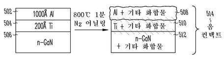
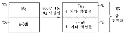
| US20110291147A1 (en) * | 2010-05-25 | 2011-12-01 | Yongjun Jeff Hu | Ohmic contacts for semiconductor structures |
| JP5236787B2 (ja) * | 2011-09-27 | 2013-07-17 | シャープ株式会社 | 窒化物半導体装置およびその製造方法 |
| CN106129216A (zh) * | 2012-11-16 | 2016-11-16 | 大连美明外延片科技有限公司 | 一种四元AlGaInP发光二极管芯片及其制造方法 |
| US9419181B2 (en) * | 2013-05-13 | 2016-08-16 | Infineon Technologies Dresden Gmbh | Electrode, an electronic device, and a method for manufacturing an optoelectronic device |
| US9425050B2 (en) | 2013-08-16 | 2016-08-23 | Avago Technologies General Ip (Singapore) Pte. Ltd. | System and method for providing an electron blocking layer with doping control |
| EP2881982B1 (en) * | 2013-12-05 | 2019-09-04 | IMEC vzw | Method for fabricating cmos compatible contact layers in semiconductor devices |
| JP6444718B2 (ja) * | 2014-12-15 | 2018-12-26 | 株式会社東芝 | 半導体装置 |
| CN104979215B (zh) * | 2015-06-23 | 2018-01-02 | 京东方科技集团股份有限公司 | 低温多晶硅薄膜晶体管及其制备方法 |
| CN105914270B (zh) * | 2016-06-28 | 2018-09-18 | 聚灿光电科技股份有限公司 | 硅基氮化镓led外延结构的制造方法 |
| US10032880B2 (en) | 2016-10-10 | 2018-07-24 | Semiconductor Components Industries, Llc | Method for forming ohmic contacts |
| TWI622188B (zh) * | 2016-12-08 | 2018-04-21 | 錼創科技股份有限公司 | 發光二極體晶片 |
| US10290719B1 (en) | 2017-12-27 | 2019-05-14 | International Business Machines Corporation | Indium gallium arsenide metal oxide semiconductor field effect transistor having a low contact resistance to metal electrode |
| CN115458649B (zh) * | 2022-10-21 | 2025-05-02 | 江西兆驰半导体有限公司 | 发光二极管外延片及其制备方法、发光二极管 |
Family Cites Families (23)
| Publication number | Priority date | Publication date | Assignee | Title |
|---|---|---|---|---|
| JPS5136138A (ja) | 1974-09-21 | 1976-03-26 | Ricoh Kk | Denshishashinkankozairyo |
| JP2509713B2 (ja) * | 1989-10-18 | 1996-06-26 | シャープ株式会社 | 炭化珪素半導体装置およびその製造方法 |
| JP3278877B2 (ja) * | 1991-11-08 | 2002-04-30 | ソニー株式会社 | 配線の形成方法 |
| JP2783349B2 (ja) * | 1993-07-28 | 1998-08-06 | 日亜化学工業株式会社 | n型窒化ガリウム系化合物半導体層の電極及びその形成方法 |
| EP1450415A3 (en) * | 1993-04-28 | 2005-05-04 | Nichia Corporation | Gallium nitride-based III-V group compound semiconductor device |
| JPH09232632A (ja) * | 1995-12-22 | 1997-09-05 | Toshiba Corp | 半導体発光素子及びその製造方法 |
| TW367528B (en) * | 1996-02-02 | 1999-08-21 | Applied Materials Inc | Titanium aluminide wetting layer for aluminum contacts |
| US5700718A (en) * | 1996-02-05 | 1997-12-23 | Micron Technology, Inc. | Method for increased metal interconnect reliability in situ formation of titanium aluminide |
| JPH09292285A (ja) * | 1996-04-30 | 1997-11-11 | Yamaha Corp | 基板温度の測定方法 |
| US5763010A (en) * | 1996-05-08 | 1998-06-09 | Applied Materials, Inc. | Thermal post-deposition treatment of halogen-doped films to improve film stability and reduce halogen migration to interconnect layers |
| JPH10125676A (ja) * | 1996-10-15 | 1998-05-15 | Fujitsu Ltd | アルミニウム配線の作製方法 |
| US6677619B1 (en) * | 1997-01-09 | 2004-01-13 | Nichia Chemical Industries, Ltd. | Nitride semiconductor device |
| JP3271657B2 (ja) * | 1997-10-09 | 2002-04-02 | 日亜化学工業株式会社 | n型窒化ガリウム系化合物半導体の電極及びその形成方法 |
| KR100333724B1 (ko) * | 1998-06-30 | 2002-09-17 | 주식회사 하이닉스반도체 | 티타늄알루미늄나이트라이드반사방지막을이용한반도체소자의금속배선형성방법 |
| JP3974284B2 (ja) * | 1999-03-18 | 2007-09-12 | 株式会社東芝 | 半導体装置の製造方法 |
| TW493287B (en) * | 2001-05-30 | 2002-07-01 | Epistar Corp | Light emitting diode structure with non-conductive substrate |
| JP4030534B2 (ja) * | 2003-07-25 | 2008-01-09 | 昭和電工株式会社 | 化合物半導体発光素子およびその製造方法 |
| JP4539844B2 (ja) * | 2004-04-15 | 2010-09-08 | セイコーエプソン株式会社 | 誘電体キャパシタおよびその製造方法ならびに半導体装置 |
| US7715885B2 (en) | 2004-06-14 | 2010-05-11 | Samsung Electronics Co., Ltd. | Power saving system in distributed wireless personal area network and method thereof |
| JP4733371B2 (ja) * | 2004-08-18 | 2011-07-27 | 三菱化学株式会社 | n型窒化物半導体用のオーミック電極およびその製造方法 |
| CN101303978A (zh) * | 2008-07-04 | 2008-11-12 | 西安电子科技大学 | 适用于氮化镓器件n型欧姆接触的制作方法 |
| CN101369599B (zh) * | 2008-07-11 | 2011-02-16 | 北京大学 | 氮化镓基器件的欧姆接触及其制备方法 |
| US20110291147A1 (en) * | 2010-05-25 | 2011-12-01 | Yongjun Jeff Hu | Ohmic contacts for semiconductor structures |
-
2010
- 2010-05-25 US US12/787,211 patent/US20110291147A1/en not_active Abandoned
-
2011
- 2011-05-25 JP JP2013512212A patent/JP2013528947A/ja active Pending
- 2011-05-25 SG SG2012086187A patent/SG185718A1/en unknown
- 2011-05-25 KR KR1020127033623A patent/KR20130071440A/ko not_active Ceased
- 2011-05-25 CN CN201180031071.2A patent/CN102947956B/zh active Active
- 2011-05-25 WO PCT/US2011/037947 patent/WO2011150089A2/en active Application Filing
- 2011-05-25 TW TW100118367A patent/TWI550907B/zh active
-
2014
- 2014-04-25 US US14/261,901 patent/US9608185B2/en active Active
-
2017
- 2017-01-05 US US15/399,372 patent/US10446727B2/en active Active
-
2019
- 2019-10-03 US US16/592,425 patent/US10998481B2/en active Active
-
2021
- 2021-04-06 US US17/223,732 patent/US20210257526A1/en not_active Abandoned
-
2024
- 2024-09-18 US US18/888,836 patent/US20250015245A1/en active Pending
Also Published As
| Publication number | Publication date |
|---|---|
| US9608185B2 (en) | 2017-03-28 |
| CN102947956B (zh) | 2016-12-28 |
| SG185718A1 (en) | 2012-12-28 |
| US20170117449A1 (en) | 2017-04-27 |
| WO2011150089A2 (en) | 2011-12-01 |
| US20140234996A1 (en) | 2014-08-21 |
| US10998481B2 (en) | 2021-05-04 |
| US20210257526A1 (en) | 2021-08-19 |
| CN102947956A (zh) | 2013-02-27 |
| JP2013528947A (ja) | 2013-07-11 |
| TWI550907B (zh) | 2016-09-21 |
| US20110291147A1 (en) | 2011-12-01 |
| US20200035891A1 (en) | 2020-01-30 |
| US20250015245A1 (en) | 2025-01-09 |
| TW201208123A (en) | 2012-02-16 |
| WO2011150089A3 (en) | 2012-03-15 |
| US10446727B2 (en) | 2019-10-15 |
Similar Documents
| Publication | Publication Date | Title |
|---|---|---|
| US20250015245A1 (en) | Ohmic contacts for semiconductor structures | |
| US7173288B2 (en) | Nitride semiconductor light emitting device having electrostatic discharge (ESD) protection capacity | |
| US7705348B2 (en) | Semiconductor light-emitting device with electrode for N-polar InGaAIN surface | |
| KR100940001B1 (ko) | Ⅲ-니트라이드 발광 장치에서 옴 접촉의 형성 | |
| US6847052B2 (en) | Light-emitting diode device geometry | |
| CN108365062B (zh) | 半导体元件 | |
| US10651340B2 (en) | Reducing or eliminating nanopipe defects in III-nitride structures | |
| TW201841227A (zh) | 半導體元件 | |
| CN111244234B (zh) | 一种可改善n型欧姆接触的深紫外LED外延片 | |
| CN115692557A (zh) | 半导体元件 | |
| US8372672B2 (en) | Nitride semiconductor light emitting device and method of manufacturing the same | |
| CN109860363B (zh) | 半导体元件 | |
| TW202501839A (zh) | 半導體元件 |
Legal Events
| Date | Code | Title | Description |
|---|---|---|---|
| PA0105 | International application |
Patent event date: 20121224 Patent event code: PA01051R01D Comment text: International Patent Application |
|
| PG1501 | Laying open of application | ||
| PA0201 | Request for examination |
Patent event code: PA02012R01D Patent event date: 20160525 Comment text: Request for Examination of Application |
|
| E902 | Notification of reason for refusal | ||
| PE0902 | Notice of grounds for rejection |
Comment text: Notification of reason for refusal Patent event date: 20170314 Patent event code: PE09021S01D |
|
| E601 | Decision to refuse application | ||
| PE0601 | Decision on rejection of patent |
Patent event date: 20170620 Comment text: Decision to Refuse Application Patent event code: PE06012S01D Patent event date: 20170314 Comment text: Notification of reason for refusal Patent event code: PE06011S01I |