KR20120099270A - Oxygen-doping for non-carbon radical-component cvd films - Google Patents
Oxygen-doping for non-carbon radical-component cvd films Download PDFInfo
- Publication number
- KR20120099270A KR20120099270A KR1020127017248A KR20127017248A KR20120099270A KR 20120099270 A KR20120099270 A KR 20120099270A KR 1020127017248 A KR1020127017248 A KR 1020127017248A KR 20127017248 A KR20127017248 A KR 20127017248A KR 20120099270 A KR20120099270 A KR 20120099270A
- Authority
- KR
- South Korea
- Prior art keywords
- oxygen
- precursor
- radical
- silicon
- nitrogen
- Prior art date
Links
Images

Classifications
-
- C—CHEMISTRY; METALLURGY
- C23—COATING METALLIC MATERIAL; COATING MATERIAL WITH METALLIC MATERIAL; CHEMICAL SURFACE TREATMENT; DIFFUSION TREATMENT OF METALLIC MATERIAL; COATING BY VACUUM EVAPORATION, BY SPUTTERING, BY ION IMPLANTATION OR BY CHEMICAL VAPOUR DEPOSITION, IN GENERAL; INHIBITING CORROSION OF METALLIC MATERIAL OR INCRUSTATION IN GENERAL
- C23C—COATING METALLIC MATERIAL; COATING MATERIAL WITH METALLIC MATERIAL; SURFACE TREATMENT OF METALLIC MATERIAL BY DIFFUSION INTO THE SURFACE, BY CHEMICAL CONVERSION OR SUBSTITUTION; COATING BY VACUUM EVAPORATION, BY SPUTTERING, BY ION IMPLANTATION OR BY CHEMICAL VAPOUR DEPOSITION, IN GENERAL
- C23C16/00—Chemical coating by decomposition of gaseous compounds, without leaving reaction products of surface material in the coating, i.e. chemical vapour deposition [CVD] processes
- C23C16/22—Chemical coating by decomposition of gaseous compounds, without leaving reaction products of surface material in the coating, i.e. chemical vapour deposition [CVD] processes characterised by the deposition of inorganic material, other than metallic material
- C23C16/30—Deposition of compounds, mixtures or solid solutions, e.g. borides, carbides, nitrides
- C23C16/308—Oxynitrides
-
- C—CHEMISTRY; METALLURGY
- C23—COATING METALLIC MATERIAL; COATING MATERIAL WITH METALLIC MATERIAL; CHEMICAL SURFACE TREATMENT; DIFFUSION TREATMENT OF METALLIC MATERIAL; COATING BY VACUUM EVAPORATION, BY SPUTTERING, BY ION IMPLANTATION OR BY CHEMICAL VAPOUR DEPOSITION, IN GENERAL; INHIBITING CORROSION OF METALLIC MATERIAL OR INCRUSTATION IN GENERAL
- C23C—COATING METALLIC MATERIAL; COATING MATERIAL WITH METALLIC MATERIAL; SURFACE TREATMENT OF METALLIC MATERIAL BY DIFFUSION INTO THE SURFACE, BY CHEMICAL CONVERSION OR SUBSTITUTION; COATING BY VACUUM EVAPORATION, BY SPUTTERING, BY ION IMPLANTATION OR BY CHEMICAL VAPOUR DEPOSITION, IN GENERAL
- C23C16/00—Chemical coating by decomposition of gaseous compounds, without leaving reaction products of surface material in the coating, i.e. chemical vapour deposition [CVD] processes
- C23C16/22—Chemical coating by decomposition of gaseous compounds, without leaving reaction products of surface material in the coating, i.e. chemical vapour deposition [CVD] processes characterised by the deposition of inorganic material, other than metallic material
- C23C16/30—Deposition of compounds, mixtures or solid solutions, e.g. borides, carbides, nitrides
- C23C16/40—Oxides
- C23C16/401—Oxides containing silicon
- C23C16/402—Silicon dioxide
-
- C—CHEMISTRY; METALLURGY
- C23—COATING METALLIC MATERIAL; COATING MATERIAL WITH METALLIC MATERIAL; CHEMICAL SURFACE TREATMENT; DIFFUSION TREATMENT OF METALLIC MATERIAL; COATING BY VACUUM EVAPORATION, BY SPUTTERING, BY ION IMPLANTATION OR BY CHEMICAL VAPOUR DEPOSITION, IN GENERAL; INHIBITING CORROSION OF METALLIC MATERIAL OR INCRUSTATION IN GENERAL
- C23C—COATING METALLIC MATERIAL; COATING MATERIAL WITH METALLIC MATERIAL; SURFACE TREATMENT OF METALLIC MATERIAL BY DIFFUSION INTO THE SURFACE, BY CHEMICAL CONVERSION OR SUBSTITUTION; COATING BY VACUUM EVAPORATION, BY SPUTTERING, BY ION IMPLANTATION OR BY CHEMICAL VAPOUR DEPOSITION, IN GENERAL
- C23C16/00—Chemical coating by decomposition of gaseous compounds, without leaving reaction products of surface material in the coating, i.e. chemical vapour deposition [CVD] processes
- C23C16/44—Chemical coating by decomposition of gaseous compounds, without leaving reaction products of surface material in the coating, i.e. chemical vapour deposition [CVD] processes characterised by the method of coating
- C23C16/448—Chemical coating by decomposition of gaseous compounds, without leaving reaction products of surface material in the coating, i.e. chemical vapour deposition [CVD] processes characterised by the method of coating characterised by the method used for generating reactive gas streams, e.g. by evaporation or sublimation of precursor materials
- C23C16/452—Chemical coating by decomposition of gaseous compounds, without leaving reaction products of surface material in the coating, i.e. chemical vapour deposition [CVD] processes characterised by the method of coating characterised by the method used for generating reactive gas streams, e.g. by evaporation or sublimation of precursor materials by activating reactive gas streams before their introduction into the reaction chamber, e.g. by ionisation or addition of reactive species
-
- C—CHEMISTRY; METALLURGY
- C23—COATING METALLIC MATERIAL; COATING MATERIAL WITH METALLIC MATERIAL; CHEMICAL SURFACE TREATMENT; DIFFUSION TREATMENT OF METALLIC MATERIAL; COATING BY VACUUM EVAPORATION, BY SPUTTERING, BY ION IMPLANTATION OR BY CHEMICAL VAPOUR DEPOSITION, IN GENERAL; INHIBITING CORROSION OF METALLIC MATERIAL OR INCRUSTATION IN GENERAL
- C23C—COATING METALLIC MATERIAL; COATING MATERIAL WITH METALLIC MATERIAL; SURFACE TREATMENT OF METALLIC MATERIAL BY DIFFUSION INTO THE SURFACE, BY CHEMICAL CONVERSION OR SUBSTITUTION; COATING BY VACUUM EVAPORATION, BY SPUTTERING, BY ION IMPLANTATION OR BY CHEMICAL VAPOUR DEPOSITION, IN GENERAL
- C23C16/00—Chemical coating by decomposition of gaseous compounds, without leaving reaction products of surface material in the coating, i.e. chemical vapour deposition [CVD] processes
- C23C16/44—Chemical coating by decomposition of gaseous compounds, without leaving reaction products of surface material in the coating, i.e. chemical vapour deposition [CVD] processes characterised by the method of coating
- C23C16/455—Chemical coating by decomposition of gaseous compounds, without leaving reaction products of surface material in the coating, i.e. chemical vapour deposition [CVD] processes characterised by the method of coating characterised by the method used for introducing gases into reaction chamber or for modifying gas flows in reaction chamber
- C23C16/45563—Gas nozzles
- C23C16/45565—Shower nozzles
-
- C—CHEMISTRY; METALLURGY
- C23—COATING METALLIC MATERIAL; COATING MATERIAL WITH METALLIC MATERIAL; CHEMICAL SURFACE TREATMENT; DIFFUSION TREATMENT OF METALLIC MATERIAL; COATING BY VACUUM EVAPORATION, BY SPUTTERING, BY ION IMPLANTATION OR BY CHEMICAL VAPOUR DEPOSITION, IN GENERAL; INHIBITING CORROSION OF METALLIC MATERIAL OR INCRUSTATION IN GENERAL
- C23C—COATING METALLIC MATERIAL; COATING MATERIAL WITH METALLIC MATERIAL; SURFACE TREATMENT OF METALLIC MATERIAL BY DIFFUSION INTO THE SURFACE, BY CHEMICAL CONVERSION OR SUBSTITUTION; COATING BY VACUUM EVAPORATION, BY SPUTTERING, BY ION IMPLANTATION OR BY CHEMICAL VAPOUR DEPOSITION, IN GENERAL
- C23C16/00—Chemical coating by decomposition of gaseous compounds, without leaving reaction products of surface material in the coating, i.e. chemical vapour deposition [CVD] processes
- C23C16/56—After-treatment
-
- H—ELECTRICITY
- H01—ELECTRIC ELEMENTS
- H01J—ELECTRIC DISCHARGE TUBES OR DISCHARGE LAMPS
- H01J37/00—Discharge tubes with provision for introducing objects or material to be exposed to the discharge, e.g. for the purpose of examination or processing thereof
- H01J37/32—Gas-filled discharge tubes
- H01J37/32009—Arrangements for generation of plasma specially adapted for examination or treatment of objects, e.g. plasma sources
- H01J37/32082—Radio frequency generated discharge
-
- H—ELECTRICITY
- H01—ELECTRIC ELEMENTS
- H01J—ELECTRIC DISCHARGE TUBES OR DISCHARGE LAMPS
- H01J37/00—Discharge tubes with provision for introducing objects or material to be exposed to the discharge, e.g. for the purpose of examination or processing thereof
- H01J37/32—Gas-filled discharge tubes
- H01J37/32009—Arrangements for generation of plasma specially adapted for examination or treatment of objects, e.g. plasma sources
- H01J37/32357—Generation remote from the workpiece, e.g. down-stream
-
- H—ELECTRICITY
- H01—ELECTRIC ELEMENTS
- H01J—ELECTRIC DISCHARGE TUBES OR DISCHARGE LAMPS
- H01J37/00—Discharge tubes with provision for introducing objects or material to be exposed to the discharge, e.g. for the purpose of examination or processing thereof
- H01J37/32—Gas-filled discharge tubes
- H01J37/32431—Constructional details of the reactor
- H01J37/3244—Gas supply means
- H01J37/32449—Gas control, e.g. control of the gas flow
-
- H—ELECTRICITY
- H01—ELECTRIC ELEMENTS
- H01L—SEMICONDUCTOR DEVICES NOT COVERED BY CLASS H10
- H01L21/00—Processes or apparatus adapted for the manufacture or treatment of semiconductor or solid state devices or of parts thereof
- H01L21/02—Manufacture or treatment of semiconductor devices or of parts thereof
- H01L21/02104—Forming layers
- H01L21/02107—Forming insulating materials on a substrate
- H01L21/02109—Forming insulating materials on a substrate characterised by the type of layer, e.g. type of material, porous/non-porous, pre-cursors, mixtures or laminates
- H01L21/02112—Forming insulating materials on a substrate characterised by the type of layer, e.g. type of material, porous/non-porous, pre-cursors, mixtures or laminates characterised by the material of the layer
- H01L21/02123—Forming insulating materials on a substrate characterised by the type of layer, e.g. type of material, porous/non-porous, pre-cursors, mixtures or laminates characterised by the material of the layer the material containing silicon
- H01L21/02164—Forming insulating materials on a substrate characterised by the type of layer, e.g. type of material, porous/non-porous, pre-cursors, mixtures or laminates characterised by the material of the layer the material containing silicon the material being a silicon oxide, e.g. SiO2
-
- H—ELECTRICITY
- H01—ELECTRIC ELEMENTS
- H01L—SEMICONDUCTOR DEVICES NOT COVERED BY CLASS H10
- H01L21/00—Processes or apparatus adapted for the manufacture or treatment of semiconductor or solid state devices or of parts thereof
- H01L21/02—Manufacture or treatment of semiconductor devices or of parts thereof
- H01L21/02104—Forming layers
- H01L21/02107—Forming insulating materials on a substrate
- H01L21/02225—Forming insulating materials on a substrate characterised by the process for the formation of the insulating layer
- H01L21/0226—Forming insulating materials on a substrate characterised by the process for the formation of the insulating layer formation by a deposition process
- H01L21/02263—Forming insulating materials on a substrate characterised by the process for the formation of the insulating layer formation by a deposition process deposition from the gas or vapour phase
- H01L21/02271—Forming insulating materials on a substrate characterised by the process for the formation of the insulating layer formation by a deposition process deposition from the gas or vapour phase deposition by decomposition or reaction of gaseous or vapour phase compounds, i.e. chemical vapour deposition
- H01L21/02274—Forming insulating materials on a substrate characterised by the process for the formation of the insulating layer formation by a deposition process deposition from the gas or vapour phase deposition by decomposition or reaction of gaseous or vapour phase compounds, i.e. chemical vapour deposition in the presence of a plasma [PECVD]
Abstract
실리콘 산화물 층의 형성 방법이 설명된다. 상기 방법은 무-탄소 실리콘-함유 전구체를 라디칼 전구체 및 라디칼-산소 전구체 모두와 동시에 조합하는 단계를 포함한다. 라디칼 전구체 및 실리콘-함유 전구체 중 하나가 질소를 포함한다. 그러한 방법은 기판 상에 실리콘-산소-및-질소-함유 층의 침착을 초래한다. 이어서, 실리콘-산소-및-질소-함유 층의 산소 함량이 증가되어 매우 적은 질소를 포함할 수 있는 실리콘 산화물 층을 형성한다. 라디칼-산소 전구체 및 라디칼 전구체가 분리된 플라즈마 및 동일한 플라즈마 내에서 생산될 수 있다. 산소-함유 대기의 존재하에서 층을 어닐링함으로써 산소 함량의 증가가 초래될 것이고 그리고 필름의 밀도는 비활성 분위기 내에서 온도를 보다 더 높게 높임으로써 추가적으로 증가될 수 있을 것이다. A method of forming a silicon oxide layer is described. The method includes combining the carbon-free silicon-containing precursor simultaneously with both the radical precursor and the radical-oxygen precursor. One of the radical precursor and the silicon-containing precursor comprises nitrogen. Such a method results in the deposition of a silicon-oxygen- and-nitrogen-containing layer on the substrate. The oxygen content of the silicon-oxygen-and-nitrogen-containing layer is then increased to form a silicon oxide layer that may contain very little nitrogen. Radical-oxygen precursors and radical precursors can be produced in separate plasmas and in the same plasma. Annealing the layer in the presence of an oxygen-containing atmosphere will result in an increase in oxygen content and the density of the film may be further increased by raising the temperature even higher in an inert atmosphere.
Description
관련 출원에 대한 교차 참조Cross-reference to related application
본원은 "비-탄소 라디칼-성분 CVD필름을 위한 산소-도핑"이라는 명칭으로 2010년 7월 15일자로 출원된 미국 특허 출원번호 제12/836,991호의 PCT 출원이며, Nintin Ingle 등이 출원한 "비-탄소 FCVD 필름을 위한 산소-도핑"이라는 명칭의 2009년 12월 2일자 미국 가특허 출원 제61/265,865호의 이익을 주장하고, 이러한 출원의 전체적인 내용은 모든 목적을 위해 본원에 인용되어 통합된다. This application is a PCT application of US Patent Application No. 12 / 836,991, filed Jul. 15, 2010, entitled "Oxygen-Doping for Non-Carbon Radical-Component CVD Films," and filed by Nintin Ingle et al. Claiming the benefit of US Provisional Patent Application No. 61 / 265,865 filed December 2, 2009 entitled "Oxygen-Doping for Carbon FCVD Films," the entire contents of which are incorporated herein by reference for all purposes.
반도체 장치의 기하 구조는 수십년 전 그들이 도입된 후에 크기가 크게 감소되었다. 현재 반도체 제조 설비는 45㎚, 32㎚ 및 28㎚의 피쳐(feature) 크기를 가진 소자들을 통상적으로 생산하며, 심지어 더 작은 기하 구조를 가지는 소자를 제조하기 위한 새로운 설비가 개발 및 작동되고 있다. 이러한 피쳐 크기의 감소는 감소된 공간 치수를 가지는 소자의 구조적 피쳐(structural features)들을 유발하게 된다. 갭 깊이 대 갭 폭의 종횡비가 유전체 물질로 갭을 충진하는 것이 문제가 되는 포인트까지, 소자의 갭과 트랜치의 폭들이 좁아졌다. 침착(depositing) 유전체 물질은, 갭이 완전히 충진되기 전에 상단부에서 막히기 쉬워서, 갭의 중간에 공극 또는 이음매(seam)을 형성하는 경향이 있다. The geometry of semiconductor devices has been greatly reduced in size after their introduction decades ago. Currently, semiconductor manufacturing facilities typically produce devices with feature sizes of 45 nm, 32 nm and 28 nm, and new facilities are being developed and operated to manufacture devices with even smaller geometries. This reduction in feature size results in structural features of the device with reduced spatial dimensions. The gaps of the device's gaps and trenches have narrowed to the point where the aspect ratio of gap depth to gap width is problematic for filling gaps with dielectric material. Depositing dielectric material tends to clog at the top before the gap is completely filled, and tends to form voids or seams in the middle of the gap.
몇 년간, 유전체 물질이 갭의 상단을 막는 것을 방지하기 위한, 또는 이미 형성된 공극이나 이음매를 "힐링(heal)"하기 위한 많은 기술들이 개발되었다. 회전 기판 표면에 액체상으로 도포될 수 있는 크게(high) 유동가능한 전구체 물질을 이용한 하나의 해결방식(예를 들어, SOG 침착 기술)이 기재되었다. 유동가능 전구체들은 공극 또는 약한 이음매를 형성하지 않는 상태로 아주 작은 기판 갭들 속으로 유동되어 그것을 채울 수 있다. 그러나, 이러한 크게 유동가능한 물질들이 일단 침착되면, 이들은 고체 유전체 물질로 경화되어야 한다. Over the years, many techniques have been developed to prevent the dielectric material from clogging the top of the gap, or to "heal" previously formed voids or seams. One solution (eg, SOG deposition technique) has been described using a high flowable precursor material that can be applied in a liquid phase to a rotating substrate surface. Flowable precursors can flow into and fill very small substrate gaps without forming voids or weak seams. However, once these highly flowable materials are deposited, they must be cured into a solid dielectric material.
많은 경우에, 실리콘 산화물과 같은 고체 유전체를 남기기 위해서, 경화 프로세스는 침착된 물질로부터 탄소와 수산기를 제거하기 위해서 열처리를 포함한다. 불행하게도, 상기 시작 탄소 및 수산기 종들은 최종 물질의 품질을 떨어뜨리는 기공을 경화된 유전체에 종종 남기게 된다. 게다가, 경화하는 유전체는 부피 수축 경향이 있고, 그러한 수축 경향은 유전체와 주위 기판의 인터페이스에 균열과 공간을 남길 수 있다. 일부 실제예에서, 경화된 유전체의 부피는 40% 만큼 또는 초과만큼 감소될 수 있다. In many cases, in order to leave a solid dielectric such as silicon oxide, the curing process involves heat treatment to remove carbon and hydroxyl groups from the deposited material. Unfortunately, the starting carbon and hydroxyl species often leave pores in the cured dielectric that degrade the quality of the final material. In addition, the curable dielectric tends to shrink in volume, which can leave cracks and space at the interface between the dielectric and the surrounding substrate. In some practical cases, the volume of the cured dielectric may be reduced by 40% or more.
그에 따라, 기판 갭 및 트랜치에 공극, 이음매, 또는 이들 양자를 발생시키지 않는 상태로, 구조화된 기판에 유전체 물질을 형성하기 위한 신규한 침착 프로세스 및 물질에 대한 요구가 있다. 또한, 부피 감소가 적은 유동가능 유전체 물질의 경화 방법 및 물질에 대한 요구가 있다. 이러한 요구들 및 다른 요구들이 본원에서 해결된다. Accordingly, there is a need for new deposition processes and materials for forming dielectric materials on structured substrates without generating voids, seams, or both in the substrate gaps and trenches. There is also a need for methods and materials for curing flowable dielectric materials with low volume reduction. These and other needs are addressed herein.
실리콘 산화물 층의 형성 방법이 설명된다. 그러한 방법은 라디칼 전구체 및 라디칼-산소 전구체 모두를 무-탄소(carbon-free) 실리콘-함유 전구체와 동시에 조합하는 단계를 포함한다. 라디칼 전구체 및 실리콘-함유 전구체 중 하나가 질소를 포함한다. 그러한 방법은 기판 상에 실리콘-산소-및-질소-함유 층의 침착을 초래한다. 이어서, 실리콘-산소-및-질소-함유 층의 산소 함량이 증가되어 매우 적은 질소를 포함할 수 있는 실리콘 산화물 층을 형성한다. 라디칼-산소 전구체 및 라디칼 전구체가 분리된 플라즈마 및 동일한 플라즈마 내에서 생산될 수 있다. 산소-함유 대기의 존재하에서 층을 어닐링함으로써 산소 함량의 증가가 초래될 것이고 그리고 필름의 밀도는 비활성 분위기 내에서 온도를 보다 더 높게 높임으로써 추가적으로 증가될 수 있을 것이다. A method of forming a silicon oxide layer is described. Such methods include the step of simultaneously combining both the radical precursor and the radical-oxygen precursor with a carbon-free silicon-containing precursor. One of the radical precursor and the silicon-containing precursor comprises nitrogen. Such a method results in the deposition of a silicon-oxygen- and-nitrogen-containing layer on the substrate. The oxygen content of the silicon-oxygen-and-nitrogen-containing layer is then increased to form a silicon oxide layer that may contain very little nitrogen. Radical-oxygen precursors and radical precursors can be produced in separate plasmas and in the same plasma. Annealing the layer in the presence of an oxygen-containing atmosphere will result in an increase in oxygen content and the density of the film may be further increased by raising the temperature even higher in an inert atmosphere.
본 발명의 실시예들은 기판 프로세싱 챔버 내에서의 무-플라즈마 기판 프로세싱 영역에서 실리콘 산화물 층을 형성하는 방법들을 포함한다. 그 방법들은 라디칼-산소 전구체를 생산하기 위해서 산소-함유 전구체를 제 2 플라즈마 영역 내로 유동시키는 동안 라디칼 전구체를 생산하기 위해서 수소-함유 전구체를 제 1 플라즈마 영역으로 유동시키는 단계; 무-플라즈마 기판 프로세싱 영역에서 라디칼 전구체 및 라디칼-산소 전구체를 무-탄소 실리콘-함유 전구체와 동시에 조합하는 단계를 포함한다. 수소-함유 전구체 및 무-탄소 실리콘-함유 전구체 중 하나 이상이 질소를 포함한다. 그 방법들은 기판 상에 실리콘-산소-및-질소-함유 층을 침착하는 단계 및 산소-함량을 증가시키고 질소-함량을 감소시켜 실리콘 산화물 층을 형성하기 위해서 상기 실리콘-산소-및-질소-함유 층을 산소-함유 대기 내의 어닐링 온도에서 어닐링하는 단계를 더 포함한다. Embodiments of the present invention include methods of forming a silicon oxide layer in a plasma-free substrate processing region in a substrate processing chamber. The methods include flowing a hydrogen-containing precursor into a first plasma region to produce a radical precursor while flowing an oxygen-containing precursor into a second plasma region to produce a radical-oxygen precursor; Simultaneously combining the radical precursor and the radical-oxygen precursor with the carbon-free silicon-containing precursor in the plasma-free substrate processing region. At least one of the hydrogen-containing precursor and the carbon-free silicon-containing precursor comprises nitrogen. The methods include depositing a silicon-oxygen-and-nitrogen-containing layer on a substrate and increasing the oxygen-content and reducing the nitrogen-content to form a silicon oxide layer to form the silicon-oxygen-and-nitrogen-containing layer. Annealing the layer at an annealing temperature in an oxygen-containing atmosphere.
추가적인 실시예들과 특징들이 이하 상세한 설명에 기재되어 있으며, 그 일부는 당업자들이 본 명세서를 검토함으로써 명료하게 이해할 수 있고 또는 본 발명의 실시에 의해서 이해할 수 있을 것이다. 본 발명의 특징 및 장점들은 본원 명세서에 기재된 기구들, 조합들 및 방법들에 의해 구현되거나 획득될 수 있을 것이다. Additional embodiments and features are set forth in the detailed description below, some of which will be apparent to those skilled in the art upon reviewing this specification or may be understood by practice of the invention. Features and advantages of the invention may be implemented or obtained by the instruments, combinations and methods described herein.
본 명세서의 나머지 부분들과 도면들을 참조하면, 본 발명의 본질과 장점을 더 이해할 수 있을 것이며, 수개의 도면에서 유사한 구성요소를 유사한 참조번호로 인용하였다.
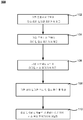
도 1은 본 발명의 실시예에 따른 실리콘 산화물 필름을 제조하기 위해 선택된 단계들을 나타낸 플로우차트이다
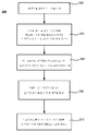
도 2는 본 발명의 실시예에 따라 챔버 플라즈마 영약을 이용하여 실리콘 산화물 필름을 형성하기 위해 선택된 단계들을 나타낸 다른 플로우차트이다.
도 3은 본 발명의 실시예에 따라 침착 동안에 O2 를 공급하면서 또는 공급하지 않으면서 얻어진 FTIR 스펙트럼의 그래프이다.
도 4는 본 발명의 실시예에 따른 기판 프로세싱 시스템을 도시한 도면이다.
도 5a는 본 발명의 실시예에 따른 기판 프로세싱 챔버를 도시한 도면이다.
도 5b는 본 발명의 실시예에 따른 기판 프로세싱 챔버의 샤워헤드를 도시한 도면이다. Referring to the remainder of the specification and the drawings, the nature and advantages of the invention will be better understood, and like reference numerals refer to like elements in the several views.
1 is a flowchart showing selected steps for producing a silicon oxide film according to an embodiment of the present invention.
FIG. 2 is another flowchart showing selected steps for forming a silicon oxide film using chamber plasma elimination in accordance with an embodiment of the present invention.
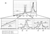
3 is a graph of the FTIR spectra obtained with or without feeding O 2 during deposition in accordance with an embodiment of the present invention.
4 illustrates a substrate processing system according to an embodiment of the invention.
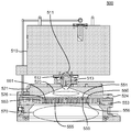
5A illustrates a substrate processing chamber in accordance with an embodiment of the present invention.
5B illustrates a showerhead of a substrate processing chamber in accordance with an embodiment of the present invention.
실리콘 산화물 층을 형성하는 방법이 설명된다. 그러한 방법은 라디칼 전구체 및 라디칼-산소 전구체 모두를 무-탄소 실리콘-함유 전구체와 동시에 조합하는 단계를 포함한다. 라디칼 전구체 및 실리콘-함유 전구체 중 하나가 질소를 포함한다. 그러한 방법은 기판 상에 실리콘-산소-및-질소-함유 층의 침착을 초래한다. 이어서, 실리콘-산소-및-질소-함유 층의 산소 함량이 증가되어 매우 적은 질소를 포함할 수 있는 실리콘 산화물 층을 형성한다. 라디칼-산소 전구체 및 라디칼 전구체가 분리된 플라즈마 및 동일한 플라즈마 내에서 생산될 수 있다. 산소-함유 대기의 존재하에서 층을 어닐링함으로써 산소 함량의 증가가 초래될 것이고 그리고 필름의 밀도는 비활성 분위기 내에서 온도를 보다 더 높게 높임으로써 추가적으로 증가될 수 있을 것이다. A method of forming a silicon oxide layer is described. Such methods include the step of simultaneously combining both the radical precursor and the radical-oxygen precursor with a carbon-free silicon-containing precursor. One of the radical precursor and the silicon-containing precursor comprises nitrogen. Such a method results in the deposition of a silicon-oxygen- and-nitrogen-containing layer on the substrate. The oxygen content of the silicon-oxygen-and-nitrogen-containing layer is then increased to form a silicon oxide layer that may contain very little nitrogen. Radical-oxygen precursors and radical precursors can be produced in separate plasmas and in the same plasma. Annealing the layer in the presence of an oxygen-containing atmosphere will result in an increase in oxygen content and the density of the film may be further increased by raising the temperature even higher in an inert atmosphere.
전적으로 정확할 수 있고 또는 그렇지 않을 수 있는 가상적인 기구에 대해서 특허청구범위의 범주를 구속함이 없이, 일부 구체사항에 대한 설명이 유리한 것으로 입증될 수 있다. 라디칼-산소 전구체 없이 무-플라즈마 영역 내에서 라디칼 전구체를 무-탄소 실리콘-및-질소-함유 전구체와 조합하여 필름을 형성하는 것은 실리콘-및-질소-함유 필름의 형성을 초래한다. 이러한 침착 방법은 비교적 개방형의 네트워크를 초래할 수 있고, 이는 낮은 온도에서 그리고 오존 내에서 필름을 경화시켜 그리고 후속하여 보다 높은 온도에서 산소-함유 대기에서 필름을 어닐링시켜 실리콘-및-질소-함유 필름이 실리콘 산화물로 변환될 수 있게 한다. 이러한 개방형의 네트워크는 산소가 필름 내로 보다 더 깊게 침투할 수 있게 하고, 기판의 방향으로 산화물 변환을 연장시킨다. 필름의 형성 동안에 라디칼-산소 전구체의 동시적인 유동을 도입하는 것은 실리콘-산소-및-질소-함유 층의 개방형 네트워크를 통한 산소의 존재를 초래한다. 침착된 바에 따른(as-deposited) 필름 내의 산소의 존재는 차후의 프로세싱 동안에 필름을 실리콘 산화물로 변환하기 위해서 개방형의 네트워크를 통해서 반드시 유동되어야 하는 산소의 양을 감소시킨다. 라디칼-산소에 대한 동시적인 노출은 산소 함량을 균질화시키는, 굴절률을 낮추는, 침착 속도를 높이는 역할을 할 수 있고 그리고 경화 단계가 감소되거나 심지어는 제거될 수 있게 한다. Description of some of the details may prove to be advantageous without restricting the scope of the claims for a hypothetical device that may or may not be entirely accurate. Combining radical precursors with carbon-free silicon-and-nitrogen-containing precursors in the plasma-free region without radical-oxygen precursors results in the formation of silicon- and-nitrogen-containing films. This deposition method can result in a relatively open network, which cures the film at low temperatures and in ozone and subsequently anneals the film in an oxygen-containing atmosphere at higher temperatures to produce a silicon-and-nitrogen-containing film. It can be converted into silicon oxide. This open network allows oxygen to penetrate deeper into the film and extends oxide conversion in the direction of the substrate. Introducing a simultaneous flow of radical-oxygen precursors during the formation of the film results in the presence of oxygen through the open network of silicon-oxygen- and-nitrogen-containing layers. The presence of oxygen in the as-deposited film reduces the amount of oxygen that must flow through the open network to convert the film to silicon oxide during subsequent processing. Simultaneous exposure to radical-oxygen can serve to speed up the deposition rate, lower the refractive index, homogenize the oxygen content, and allow the curing step to be reduced or even eliminated.
예시적 실리콘 산화물 형성 프로세스Exemplary Silicon Oxide Formation Process
도 1은 본 발명의 실시예에 따른 실리콘 산화물 필름의 제조 방법(100)에서 선택된 단계들을 나타낸 플로우차트이다. 상기 방법(100)은 기판 프로세싱 영역에 무-탄소 실리콘 전구체를 제공하는 단계(102)를 포함한다. 상기 무-탄소 실리콘 전구체는, 다른 클래스(class)의 실리콘 전구체들 중, 예를 들어, 실리콘-및-질소 전구체, 실리콘-및-수소 전구체, 또는 실리콘-및-질소-함유 전구체일 수 있다. 실리콘 전구체는 무-탄소일 뿐만 아니라 무-산소일 수 있다. 산소의 결핍은 상기 전구체들로부터 형성된 실리콘-및-질소층에서 실라놀(Si-OH)기의 농도를 낮추게 된다. 침착된 필름에서 과다한 실라놀 부분(moieties)은 침착된 층으로부터 히드록실(-OH) 부분을 제거하는 침착후의 단계에서 공극율과 수축율의 증가를 초래할 수 있다. 1 is a flowchart illustrating steps selected in a
무-탄소 실리콘 전구체들 중 특별한 예로서는, 다른 시릴-아민들 중의 H2N(SiH3), HN(SiH3)2 및 N(SiH3)3와 같은 시릴-아민들이 포함될 수 있다. 시릴-아민의 유량은 여러 가지 실시예에서 약 200sccm 또는 그 초과, 약 300sccm 또는 그 초과, 또는 약 500sccm 또는 그 초과일 수 있다. 본 명세서에서 제시된 모든 유량은 이중 챔버 기판 프로세싱 시스템을 인용한다. 단일 웨이퍼 시스템은 이 유량들의 절반을 필요로 할 것이며, 다른 웨이퍼 크기는 프로세싱되는 영역의 축척에 따른 유량을 필요로 할 것이다. 이 시릴-아민들은 캐리어 가스, 반응 가스 또는 양자 모두로서 작용할 수 있는 추가적인 가스들과 혼합될 수 있다. 이들의 추가적인 가스들의 예로서는, H2, N2, NH3, He 및 Ar 등등이 포함될 수 있다. 또한, 무-탄소 실리콘 전구체의 예로서는 단독 실란(SiH4), 또는 다른 실리콘-함유 가스(예를 들어, N(SiH3)3), 수소 함유 가스(예를 들어, H2), 및/또는 질소 함유 가스(예를 들어, N2, NH3)와 혼합된 실란이 포함될 수도 있다. 또한, 무-탄소 실리콘 전구체는 디실란, 트리실란, 더 고차원(higher-order)의 실란들, 및 염소화된 실란, 이들 단독 또는 서로 간의 또는 전술한 무-탄소 실리콘 전구체들과의 조합을 포함할 수 있다. As a particular example of carbon-free silicon precursors, silyl-amines such as H 2 N (SiH 3 ), HN (SiH 3 ) 2 and N (SiH 3 ) 3 among other silyl-amines may be included. The flow rate of the silyl-amine may be about 200 sccm or more, about 300 sccm or more, or about 500 sccm or more in various embodiments. All flow rates presented herein refer to dual chamber substrate processing systems. A single wafer system would require half of these flow rates, while other wafer sizes would require flow rates depending on the scale of the area being processed. These silyl-amines can be mixed with additional gases that can act as a carrier gas, reactant gas or both. Examples of these additional gases may include H 2 , N 2 , NH 3 , He, Ar, and the like. In addition, examples of carbon-free silicon precursors include single silane (SiH 4 ), or other silicon-containing gas (eg, N (SiH 3 ) 3 ), hydrogen-containing gas (eg, H 2 ), and / or Silanes mixed with nitrogen containing gases (eg N 2 , NH 3 ) may also be included. Carbon-free silicon precursors may also include disilanes, trisilanes, higher-order silanes, and chlorinated silanes, alone or in combination with one another or with the carbon-free silicon precursors described above. Can be.
상기 기판 프로세싱 영역에 라디칼-질소 전구체가 제공될 수도 있다(104). 상기 라디칼-질소 전구체는 더 안정한 질소 전구체로부터 기판 프로세싱 영역의 외부에서 발생된 질소 라디칼 함유 전구체이다. 예를 들어, NH3, 히드라진(N2H4) 및/또는 N2를 함유한 안정한 질소 전구체 화합물이 프로세싱 챔버 외부의 원격 플라즈마 시스템(RPS) 또는 챔버 플라즈마 영역에서 활성화되어 라디칼-질소 전구체를 형성할 수 있으며, 그 후, 라디칼-질소 전구체는 기판 프로세싱 영역으로 운반된다. 또한, 상기 안정한 질소 전구체는, 여러 가지 실시예에서, NH3 & N2, NH3 & H2, NH3 & N2 & H2, 및 N2 & H2를 포함한 혼합물일 수도 있다. 히드라진이 N2 및 H2와의 혼합물에서 NH3와 조합하여 또는 그 대신에 사용될 수 있다. 안정한 질소 전구체의 유량은 여러 가지 실시예에서 약 300sccm 또는 그 초과, 약 500sccm 또는 그 초과, 또는 약 700sccm 또는 그 초과일 수 있다. 챔버 플라즈마 영역에서 생성된 라디칼-질소 전구체는 ·N, ·NH, ·NH2 등 중 하나 또는 그 초과일 수 있으며, 플라즈마에서 형성된 이온화된 종들을 수반할 수도 있다. A radical-nitrogen precursor may be provided 104 to the substrate processing region. The radical-nitrogen precursor is a nitrogen radical containing precursor generated outside of the substrate processing region from a more stable nitrogen precursor. For example, a stable nitrogen precursor compound containing NH 3 , hydrazine (N 2 H 4 ) and / or N 2 is activated in a remote plasma system (RPS) or chamber plasma region outside the processing chamber to form a radical-nitrogen precursor. Thereafter, the radical-nitrogen precursor is transported to the substrate processing region. In addition, the stable nitrogen precursor is, in various embodiments, NH 3 & N 2 , NH 3 & H 2 , NH 3 & N 2 & H 2 , and N 2 Or a mixture comprising & H 2 . Hydrazine may be used in combination with or instead of NH 3 in a mixture with N 2 and H 2 . The flow rate of the stable nitrogen precursor may be about 300 sccm or more, about 500 sccm or more, or about 700 sccm or more in various embodiments. The radical-nitrogen precursor produced in the chamber plasma region may be one or more of: N, NH, NH 2 , or the like, and may involve ionized species formed in the plasma.
챔버 플라즈마 영역을 채용하는 실시예에서, 라디칼-질소 전구체가 침착 영역으로부터 구획된 기판 프로세싱 영역의 섹션 내에서 생성되며, 여기에서 전구체들이 혼합되고 반응하여 침착 기판(예를 들어, 반도체 웨이퍼) 상에 실리콘-및-질소 층을 침착한다. In an embodiment employing a chamber plasma region, a radical-nitrogen precursor is created in a section of the substrate processing region partitioned from the deposition region, where the precursors are mixed and reacted on the deposition substrate (eg, semiconductor wafer). A silicon-and-nitrogen layer is deposited.
라티칼-산소 전구체가 무-플라즈마 기판 프로세싱 영역(106)으로 동시에 제공된다. 라디칼-산소 전구체는 보다 안정한 산소-함유 전구체로부터 무-플라즈마 기판 프로세싱 영역 외부에서 생성된 산소-라디칼-함유 전구체이다. 예를 들어, O2, O3, H2O, H2O2, NO, NO2 및/또는 N2O를 함유하는 안정한 산소-함유 전구체 화합물이 챔버 플라즈마 영역 내에서 또는 프로세싱 챔버 외부의 원격 플라즈마 시스템(RPS) 내에서 활성화되어 라디칼-산소 전구체를 형성할 수 있으며, 이는 다시 무-플라즈마 기판 프로세싱 영역 내로 이송된다. 라디칼-산소 전구체가 라디칼-질소 전구체와 동일한 플라즈마(챔버 플라즈마 영역 또는 공통 RPS 내) 내에서 생성될 수 있으며, 이러한 경우에 보다 안정한-산소-함유 전구체 및 보다 안정한 질소-함유 전구체가 플라즈마 영역 내에서 조합되거나 함께 조합되고 플라즈마 영역 내로 유동될 수 있다. 그 대신에, 라디칼-산소 전구체가 독립된 플라즈마 영역 내에서 발생될 수 있고, 예를 들어 라디칼-산소 전구체가 RPS 내에서 발생될 수 있고 그리고 라디칼-질소 전구체가 챔버 플라즈마 영역 내에서 발생될 수 있다. 다른 실시예들에서, 안정한 산소 전구체의 유량은 약 50sccm 보다 클 수 있고, 약 100sccm 보다 클 수 있으며, 약 150sccm이거나 그보다 클 수 있고, 약 200 이거나 그보다 클 수 있으며 또는 약 250sccm이거나 그보다 클 수 있다. 다른 실시예들에서, 안정한 산소 전구체의 유량은 약 600sccm이거나 그 보다 작을 수 있고, 약 500sccm이거나 그 보다 작을 수 있으며, 약 400sccm이거나 그 보다 작을 수 있고 또는 약 300sccm이거나 그 보다 작을 수 있다. 이들 상한 경계들 중 임의의 경계가 하한 경계들 중 임의의 경계와 조합되어 부가적인 기재된 실시예에 따른 안정한 산화물 전구체의 유량에 대한 부가적인 범위를 형성할 수 있다. A radical-oxygen precursor is simultaneously provided to the plasma-free
대략적으로 말해서, 질소를 포함하지 않는 라디칼 전구체가 또한 실리콘-및-질소-함유 층이 형성되게 할 것이다. 라디칼 전구체가 전술한 전구체들을 이용하여 원격 플라즈마 영역으로 공급된 질소를 포함한다면, 라디칼 전구체가 라디칼-질소 전구체가 될 수 있을 것이다. 라디칼 전구체는 침착 영역으로부터 구획된 반응 챔버의 섹션 내에서 발생되며, 여기에서 전구체들이 혼합되고 그리고 반응하여 침착 기판(예를 들어, 반도체 웨이퍼) 상에 실리콘-및-질소 층을 침착한다. 라디칼 전구체가 라디칼-질소 전구체인 실시예에서, 안정한 질소 전구체가 원격 플라즈마 영역 내로 흐르고 그리고 플라즈마에 의해서 여기된다. 안정한 질소 전구체(및 라디칼-질소 전구체)가 또한 수소(H2), 질소(N2), 아르곤, 헬륨 등과 같은 캐리어 가스를 수반할 수 있다. 필수적으로 질소(N2)(부가적인 비활성 캐리어 가스가 있거나 또는 없는 상태에서)로 이루어진 입력 가스로부터 형성된 라디칼-질소 전구체는 또한 설명된 실시예들에서 유리한 필름들을 생산한다는 것을 발견하였다. 라디칼-질소 전구체는 또한 실리콘-함유 전구체가 질소를 포함하는 실시예에서 수소(H2)(및 선택적으로 비활성 캐리어 가스)로 필수적으로 구성되는 입력 가스로부터 형성된 라디칼 전구체에 의해서 대체될 수 있다. Roughly speaking, radical precursors that do not contain nitrogen will also cause the silicon-and-nitrogen-containing layer to form. If the radical precursor comprises nitrogen supplied to the remote plasma region using the precursors described above, the radical precursor may be a radical-nitrogen precursor. Radical precursors are generated in sections of the reaction chamber partitioned from the deposition region, where the precursors are mixed and react to deposit a silicon-and-nitrogen layer on the deposition substrate (eg, semiconductor wafer). In an embodiment where the radical precursor is a radical-nitrogen precursor, a stable nitrogen precursor flows into the remote plasma region and is excited by the plasma. Stable nitrogen precursors (and radical-nitrogen precursors) may also involve carrier gases such as hydrogen (H 2 ), nitrogen (N 2 ), argon, helium and the like. It has been found that radical-nitrogen precursors formed from input gas consisting essentially of nitrogen (N 2 ) (with or without additional inert carrier gas) also produce advantageous films in the described embodiments. The radical-nitrogen precursor may also be replaced by a radical precursor formed from an input gas consisting essentially of hydrogen (H 2 ) (and optionally an inert carrier gas) in embodiments where the silicon-containing precursor comprises nitrogen.
기판 프로세싱 영역에서, 라디칼-질소 전구체 및 라디칼-산소 전구체의 동시적인 유동이 무-탄소 실리콘 전구체(이는 플라즈마에 의해서 상당히 여기되지 않았다)와 혼합되고 반응하여 침착 기판(108) 상에 실리콘-산소-및-질소-함유 필름을 침착한다. 낮은 유량(느린 침착 속도)의 경우에 침착된 실리콘-및-질소-함유 필름이 등각적으로(conformally) 침착될 수 있다. 다른 실시예에서, 침착된 실리콘-및-질소-함유 필름은 통상적인 실리콘 질화물(Si3N4) 필름 침착 기술과 다른 유동가능 특성을 가진다. 포메이션(formation)의 유동가능 특성은 필름이 기판의 침착 표면 상의 좁은 갭, 트랜치 및 다른 구조물로 흘러들어갈 수 있도록 한다. In the substrate processing region, simultaneous flow of the radical-nitrogen precursor and the radical-oxygen precursor mixes with and reacts with the carbon-free silicon precursor (which was not significantly excited by the plasma) to react the silicon-oxygen-on the
유동성은 라디칼-질소 전구체와 무-탄소 실리콘 전구체의 혼합에 기인한 다양한 특성 때문일 수 있다. 이 특성들은 침착된 필름에서 상당한 수소 성분 및/또는 단쇄형(short chained) 폴리실라잔 폴리머의 존재를 포함할 수 있다. 이러한 단쇄들이 성장하여 연결(network)됨으로써, 필름 형성시 및 그 후에 더 치밀한 유전체 물질을 형성한다. 예를 들면, 침착된 필름은 실라잔 타입의 Si-NH-Si 백본(backbone)(즉, Si-N-H 필름)을 가질 수 있다. 실리콘 전구체와 라디칼-질소 전구체들이 양자 모두가 무-탄소인 경우, 침착되는 실리콘-및-질소-함유 필름도 실질적으로 무-탄소이다. 물론, "무-탄소"는 필름이 필수적으로 극소량의 탄소도 갖지 않는다는 것을 의미하는 것은 아니다. 탄소 오염물질은 상기 침착된 실리콘-및-질소 전구체 상태가 되려고 하는 전구체 물질에 존재할 수 있다. 그러나, 이들 탄소 불순물의 양은 탄소 부분(예를 들어, TEOS, TMDSO 등)을 가진 실리콘 전구체에서 발견되는 것 보다 훨씬 더 작다. 침착된 실리콘-산소-및-질소-함유 필름의 유동성은 본원에서 언급된 실시예들에서 개략적으로 설명된 유량의 경우에 크게 손상되지 않는다. The fluidity can be due to various properties due to the mixing of the radical-nitrogen precursor and the carbon-free silicon precursor. These properties may include the presence of significant hydrogen components and / or short chained polysilazane polymers in the deposited film. These short chains grow and network to form denser dielectric material during and after film formation. For example, the deposited film may have a Si-NH-Si backbone (ie, Si-N-H film) of silazane type. If both the silicon precursor and the radical-nitrogen precursors are carbon-free, the silicon-and-nitrogen-containing film deposited is also substantially carbon-free. Of course, "carbon-free" does not mean that the film is essentially free of trace amounts of carbon. Carbon contaminants may be present in the precursor material that is about to become the deposited silicon-and-nitrogen precursor state. However, the amount of these carbon impurities is much smaller than that found in silicon precursors with carbon portions (eg, TEOS, TMDSO, etc.). The flowability of the deposited silicon-oxygen-and-nitrogen-containing film is not significantly impaired in the case of the flow rates outlined in the embodiments mentioned herein.
실리콘-산소-및-질소-함유 층의 침착에 이어서, 침착 기판은 산소-함유 대기에서 어닐링될 수 있다(110). 침착 기판은 산소-함유 대기가 도입될 때 경화를 위해 사용된 동일한 기판 프로세싱 영역에 잔류할 수 있거나, 또는 상기 기판은 산소-함유 대기가 도입되는 다른 챔버로 전달될 수 있다. 상기 산소-함유 대기는, 다른 산소 함유 가스들 중, 분자 산소(O2), 오존(O3), 수증기(H2O), 과산화수소(H2O2) 및 질소 산화물(NO, NO2 등)과 같은 하나 또는 그 초과의 산소 함유 가스를 포함할 수 있다. 상기 산소-함유 대기는 산소 원자(O), 수산화물(OH) 등과 같은 라디칼 산소 및 히드록실 종을 또한 포함할 수 있으며, 이들은 원격지에서 발생되어 기판 챔버로 전달될 수 있다. 또한, 산소 함유종의 이온이 존재할 수 있다. 여러 가지 실시예에서, 상기 기판의 산소 어닐링 온도는 약 1100℃ 또는 그 미만, 약 1000℃ 또는 그 미만, 약 900℃ 또는 그 미만, 또는 약 800℃ 또는 그 미만일 수 있다. 여러 가지 실시예에서, 상기 기판의 온도는 약 500℃ 또는 그 초과, 약 600℃ 또는 그 초과, 약 700℃ 또는 그 초과, 또는 약 800℃ 또는 그 초과일 수 있다. 다시 한번, 부가적으로 설명된 실시예에 따라 부가적인 기판 온도 범위를 형성하기 위해, 임의의 상한이 임의의 하한과 조합될 수 있다. Following deposition of the silicon-oxygen-and-nitrogen-containing layer, the deposition substrate may be annealed in an oxygen-containing atmosphere (110). The deposited substrate may remain in the same substrate processing region used for curing when the oxygen-containing atmosphere is introduced, or the substrate may be transferred to another chamber into which the oxygen-containing atmosphere is introduced. The oxygen-containing atmosphere is, among other oxygen-containing gases, molecular oxygen (O 2 ), ozone (O 3 ), water vapor (H 2 O), hydrogen peroxide (H 2 O 2 ) and nitrogen oxides (NO, NO 2, etc.). One or more oxygen-containing gases, such as). The oxygen-containing atmosphere may also include radical oxygen and hydroxyl species, such as oxygen atoms (O), hydroxides (OH), and the like, which may be generated remotely and delivered to the substrate chamber. In addition, ions of oxygen containing species may be present. In various embodiments, the oxygen annealing temperature of the substrate may be about 1100 ° C. or less, about 1000 ° C. or less, about 900 ° C. or less, or about 800 ° C. or less. In various embodiments, the temperature of the substrate may be about 500 ° C. or above, about 600 ° C. or above, about 700 ° C. or above, or about 800 ° C. or above. Once again, any upper limit can be combined with any lower limit to form additional substrate temperature ranges according to additionally described embodiments.
산소 어닐링 동안 기판 프로세싱 영역에 플라즈마가 존재하거나 존재하지 않을 수 있다. CVD 챔버로 유입되는 산소-함유 가스는 기판 프로세싱 영역으로 유입되기 전에 활성화된(예를 들어, 라디칼화된, 이온화된, 등) 하나 또는 그 초과의 화합물을 포함할 수 있다. 예를 들어, 상기 산소-함유 가스는, 원격 플라즈마 소오스를 통해, 또는 샤워헤드에 의해 기판 프로세싱 영역으로부터 분리된 챔버 플라즈마 영역을 통해, 더 안정한 전구체 화합물을 노출함으로써 활성화된 라디칼-산소 종, 라디칼 히드록실 종 등을 포함할 수 있다. 상기 더 안정한 전구체들은 히드록실(OH) 라디칼 및 이온을 생성하는 수증기와 과산화수소(H2O2), 그리고 산소 원자(O) 라디칼 및 이온을 생성하는 산소 분자 및/또는 오존을 포함할 수 있다. Plasma may or may not be present in the substrate processing region during oxygen annealing. The oxygen-containing gas entering the CVD chamber may include one or more compounds that are activated (eg, radicalized, ionized, etc.) prior to entering the substrate processing region. For example, the oxygen-containing gas may be activated via a remote plasma source, or through a chamber plasma region separated from the substrate processing region by a showerhead, to expose more stable precursor compounds to radical-oxygen species, radical hydrides. Roxyl species and the like. The more stable precursors may include water vapor to generate hydroxyl (OH) radicals and ions and hydrogen peroxide (H 2 O 2 ), and oxygen molecules and / or ozone to generate oxygen atom (O) radicals and ions.
상당한 산소 함량이 이미 실리콘-산소-및-질소-함유 필름 내에 존재한다면 경화 작업은 불필요할 수 있다. 그러나, 원한다면, 경화 작업이 어닐링 작업에 앞서서 도입될 수 있을 것이다. 경화 동안에, 침착 기판이 경화를 위한 기판 프로세싱 내에서 잔류될 수 있거나, 기판은 산소-함유 대기가 도입되는 다른 챔버로 전달될 수 있다. 다른 실시예들에서, 기판의 경화 온도가 약 400 ℃이거나 그 보다 작을 수 있고, 약300 ℃이거나 그 보다 작을 수 있고, 약 250 ℃이거나 그 보다 작을 수 있으며, 200 ℃이거나 그 보다 작을 수 있고, 또는 약 150 ℃이거나 그 보다 작을 수 있다. 다른 실시예들에서, 기판의 온도가 대략적으로 상온이거나 그 보다 높을 수 있고, 약 50 ℃이거나 그 보다 높을 수 있고, 약 100 ℃이거나 그 보다 높을 수 있고, 약 150 ℃이거나 그 보다 높을 수 있고, 또는 200 ℃이거나 그 보다 높을 수 있다. 상한 경계들 중 임의의 경계가 하한 경계들 중 임의의 경계와 조합되어 부가적인 설명된 실시예에 따른 기판 온도에 대한 부가적인 범위를 형성할 수 있다. 실시예들에서, 인접한 표면 네트워크에 근접할 수 있는 원자 산소의 발생을 방지하기 위해서 그리고 표면 산화를 방지기 위해서, 플라즈마가 기판 프로세싱 영역 내에 존재하지 않는다. 경화 단계 동안에 기판 프로세싱 영역으로의 오존의 유량이 약 200 sccm이거나 그 보다 높을 수 있고, 약 300 sccm이거나 그 보다 높을 수 있으며, 또는 약 500 sccm이거나 그 보다 높을 수 있다. 경화 단계 동안에 오존의 부분압이 약 10 Torr이거나 그 보다 높을 수 있고, 약 20 Torr이거나 그 보다 높을 수 있고 또는 약 40 Torr이거나 그 보다 높을 수 있다. 일부 조건(예를 들어, 약 100 ℃로부터 약 200 ℃까지의 기판 온도 사이)하에서, 변환이 실질적으로 완전한 것으로 확인되었고 그에 따라 산소-함유 분위기 내에서 비교적 높은 온도의 어닐링이 실시예들에서 불필요할 수 있다. Curing operations may be unnecessary if a significant oxygen content is already present in the silicon-oxygen- and-nitrogen-containing film. However, if desired, a curing operation may be introduced prior to the annealing operation. During cure, the deposited substrate may remain within the substrate processing for cure, or the substrate may be transferred to another chamber into which an oxygen-containing atmosphere is introduced. In other embodiments, the curing temperature of the substrate may be about 400 ° C. or less, about 300 ° C. or less, about 250 ° C. or less, 200 ° C. or less, Or about 150 ° C. or less. In other embodiments, the temperature of the substrate may be approximately room temperature or higher, about 50 ° C. or higher, about 100 ° C. or higher, about 150 ° C. or higher, Or 200 ° C. or higher. Any of the upper bounds may be combined with any of the lower bounds to form an additional range for substrate temperature according to the additional described embodiment. In embodiments, no plasma is present in the substrate processing region to prevent the generation of atomic oxygen that may be in proximity to adjacent surface networks and to prevent surface oxidation. The flow rate of ozone to the substrate processing region during the curing step may be about 200 kScm or higher, about 300 kScm or higher, or about 500 kScm or higher. During the curing step the partial pressure of ozone may be about 10 Torr or higher, about 20 Torr or higher, or about 40 Pa Torr or higher. Under some conditions (eg, between substrate temperatures from about 100 ° C. to about 200 ° C.), the conversion has been found to be substantially complete and thus a relatively high temperature annealing in an oxygen-containing atmosphere may be unnecessary in embodiments. Can be.
경화 및 산소 어닐링 양자 모두의 산소-함유 대기는 실리콘-산소-및-질소-함유 필름을 실리콘 산화물(SiO2) 필름으로 변환시키기 위한 산소를 제공한다. 앞서 주목한 바와 같이, 실리콘-산소-및-질소-함유 필름에서의 산소의 결핍은 최종 실리콘 산화물 필름에 현저히 적은 기공이 형성되는 결과를 초래한다. 또한, 실리콘 산화물로의 변환시 필름의 부피 감소(즉, 수축)를 적게 하는 결과를 초래한다. 예를 들어, 탄소-함유 실리콘 전구체로부터 형성되는 실리콘-질소-탄소 층은 실리콘 산화물로 변환될 때 40 부피% 또는 그 초과만큼 수축할 수 있는 반면, 실질적인 무-탄소 실리콘-및-질소 필름은 약 15 부피% 또는 그 미만만큼 수축할 수 있다. The oxygen-containing atmosphere of both the curing and oxygen annealing provides oxygen for converting the silicon-oxygen-and-nitrogen-containing film into a silicon oxide (SiO 2 ) film. As noted earlier, the lack of oxygen in the silicon-oxygen-and-nitrogen-containing film results in the formation of significantly less pores in the final silicon oxide film. It also results in less volume reduction (ie shrinkage) of the film upon conversion to silicon oxide. For example, a silicon-nitrogen-carbon layer formed from a carbon-containing silicon precursor may shrink by 40% by volume or more when converted to silicon oxide, while a substantially carbon-free silicon-and-nitrogen film is about Shrink by 15% or less.
도 2를 참조하면, 본 발명의 실시예에 따른 기판 갭(트렌치)에 실리콘 산화물 필름을 형성하는 방법(200)에서 선택된 단계들을 도시하는 플로우차트가 도시되어 있다. 상기 방법(200)은 갭을 포함한 기판을 기판 프로세싱 영역으로 전송하는 단계(작업 202)를 포함할 수 있다. 상기 기판은 당해 기판 상에 형성된 장치 요소(예를 들어, 트랜지스터)들의 구조와 간격을 위한 복수의 갭을 가질 수 있다. 상기 갭은 1:1 보다 훨씬 더 큰 높이 대 폭(즉, H/W)의 종횡비(AR)(예를 들어, 5:1 또는 그 초과, 6:1 또는 그 초과, 7:1 또는 그 초과, 8:1 또는 그 초과, 9:1 또는 그 초과, 10:1 또는 그 초과, 11:1 또는 그 초과, 12:1 또는 그 초과, 등)를 규정하는 높이와 폭을 가질 수 있다. 많은 경우에서, 높은 종횡비는 약 90㎚ 내지 약 22㎚ 또는 그 미만의 범위인 작은 갭 폭(예를 들어, 약 90㎚ 미만, 65㎚, 50㎚, 45㎚, 32㎚, 22㎚, 16㎚ 등) 때문이다. Referring to FIG. 2, there is shown a flowchart depicting steps selected in a
챔버 플라즈마 영역으로의 안정한 질소 전구체 및 안정한 산소 전구체의 동시적인 유동은 라디칼-질소 전구체 및 라디칼-산소 전구체를 형성한다(작업 204). 플라즈마에 의해서 상당히 여기되지 않은 무-탄소 실리콘 전구체가 무-플라즈마 기판 프로세싱 영역 내에서 라디칼-질소와 라디칼-산소 전구체와 혼합된다(작업 206). 유동가능 실리콘-산소-및-질소-함유 층이 기판에 침착될 수 있다(작업 208). 상기 층이 유동가능하기 때문에, 충진 물질의 중앙 주변에 공극 또는 약한 이음매를 형성하지 않고 높은 종횡비의 갭을 충진할 수 있다. 예를 들어, 침착되는 유동가능 물질은 갭이 완전히 충진되기 전에 갭의 상단을 미리 막아 갭의 중간에 공극을 남기는 경우가 거의 없다. Simultaneous flow of a stable nitrogen precursor and a stable oxygen precursor into the chamber plasma region forms a radical-nitrogen precursor and a radical-oxygen precursor (operation 204). Carbon-free silicon precursor that is not significantly excited by the plasma is mixed with radical-nitrogen and radical-oxygen precursors within the plasma-free substrate processing region (operation 206). A flowable silicon-oxygen- and-nitrogen-containing layer can be deposited on the substrate (operation 208). Since the layer is flowable, it is possible to fill high aspect ratio gaps without forming voids or weak seams around the center of the fill material. For example, the flowable material that is deposited rarely leaves a void in the middle of the gap, pre-closing the top of the gap before the gap is completely filled.
이어서, 침착된 바에 따른 실리콘-산소-및-질소-함유 층은 산소-함유 대기에서 어닐링될 수 있고(작업 210), 이에 따라 실리콘-산소-및-질소-함유 층이 실리콘 산화물로 변환된다. 상기 실리콘 산화물 층을 조밀화하기 위해 더 높은 기판 온도의 비활성 분위기에서 추가적인 어닐링(도시하지 않음)이 실시될 수 있다. The silicon-oxygen-and-nitrogen-containing layer as deposited can then be annealed in an oxygen-containing atmosphere (operation 210), thereby converting the silicon-oxygen-and-nitrogen-containing layer to silicon oxide. Further annealing (not shown) may be performed in an inert atmosphere at a higher substrate temperature to densify the silicon oxide layer.
다시, 실리콘 산화물로의 변환을 보조하기 위해서 경화 단계가 실행될 수 있을 것이고 그리고 그 경화 단계는 필름 형성(작업 206)과 어닐링 작업(210) 사이에서 이루어질 것이다. Again, a curing step may be performed to assist in the conversion to silicon oxide and the curing step will take place between film formation (operation 206) and
산소-함유 대기에서 침착된 바에 따른 실리콘-산소-및-질소-함유 층을 어닐링하는 것은 기판 갭을 포함하여 기판 상에 실리콘 산화물층을 형성한다(210). 실시예에서, 경화 및 어닐링의 프로세싱 매개변수는 도 1과 관련하여 설명한 동일한 범위를 가진다. 전술한 바와 같이, 열처리 단계 전에 당해 층에 상당량의 탄소가 존재하고 탄소 함유 전구체로 형성된 유사한 층보다 상기 실리콘 산화물층이 기공이 적고 부피 감소가 작다. 많은 경우에서, 부피 감소는 수축하는 실리콘 산화물로 인하여 갭에 형성되는 공간을 채우고, 힐링 또는 달리 제거하기 위한 사후 열처리 단계들을 피할 수 있을 정도로 충분하하게 작다(예를 들어, 약 15부피% 또는 그 미만).Annealing the silicon-oxygen-and-nitrogen-containing layer as deposited in an oxygen-containing atmosphere forms a silicon oxide layer on the substrate, including the substrate gap (210). In an embodiment, the processing parameters of curing and annealing have the same ranges described in connection with FIG. 1. As mentioned above, a significant amount of carbon is present in the layer prior to the heat treatment step and the silicon oxide layer has less porosity and smaller volume reduction than similar layers formed of carbon containing precursors. In many cases, the volume reduction is small enough (e.g., about 15% by volume or so to avoid post-heating steps to fill the spaces formed in the gap due to shrinking silicon oxide and to heal or otherwise remove) under).
본 발명을 보다 잘 이해하고 평가할 수 있게 하기 위해서, 2개의 필름; 즉, 도 2의 프로세스 유동에 따라 성장된 제 1 필름 및 라디칼-산소 전구체 없이 성장된 다른 유사한 제 2 필름을 인용한다. 샤워헤드에 의해서 무-플라즈마 기판 프로세싱 영역으로부터 분리된 챔버 플라즈마 영역 내로 275sccm의 유량으로 무-탄소 실리콘-및-질소-함유 전구체가 전달되고 550sccm의 유량으로 암모니아(NH3)가 전달됨에 따라 각 필름이 TSA와 함께 성장되었다. 분자 산소(O2)는 암모니아를 위해서 사용된 유입구와 분리된 유입구를 통해서 챔버 플라즈마 영역 내로 또한 150sccm의 유량으로 전달되었다. 분자 산소가 제 1 필름의 성장 동안에 전달되었으나 제 2 필름의 성장 동안에는 전달되지 않았다. 제 1 필름은 4800Å/분의 침착 속도로 성장되는 반면, 제 2 필름은 1650Å/분의 침착 속도로 성장되었다. 빠른 침착 속도는 전술한 바와 같은 독립적인 경화 작업에 대한 의존도 감소에 더한 추가적인 장점이 된다. 제 1 필름의 굴절률(1.529)은 또한 제 2 필름(1.5374)의 굴절률 보다 낮으며, 이는 침착에 따른 필름이 실리콘 산화물에 대한 굴절률(1.46)에 더 근접한다는 것을 나타낸다. In order to be able to better understand and evaluate the present invention, two films; That is, we cite the first film grown according to the process flow of FIG. 2 and another similar second film grown without radical-oxygen precursors. Each film was delivered by a showerhead into a chamber plasma region separated from the plasma-free substrate processing region at a flow rate of 275 sccm and ammonia (NH 3 ) at a flow rate of 550 sccm. It was grown with TSA. Molecular oxygen (O 2 ) was delivered into the chamber plasma region and at a flow rate of 150 sccm through an inlet separate from the inlet used for ammonia. Molecular oxygen was delivered during the growth of the first film but not during the growth of the second film. The first film was grown at a deposition rate of 4800 mm 3 / min, while the second film was grown at a deposition rate of 1650 mm 3 / min. Fast deposition rates are an additional advantage in addition to reducing the dependence on independent curing operations as described above. The refractive index (1.529) of the first film is also lower than the refractive index of the second film (1.5374), indicating that the film upon deposition is closer to the refractive index (1.46) for silicon oxide.
도 3은 본 발명의 실시예에 따라 침착 동안에 O2가 공급되지 않는 상태에서 그리고 공급되는 상태에서 획득한 FTIR 스펙트럼을 도시한 그래프이다. 유량은 TSA의 경우에 275sccm이었고, NH3의 경우에 550sccm이었으며, 산소(사용되는 경우)의 경우에 150sccm이었다. 무-플라즈마 기판 프로세싱 영역 내에서 TSA와 조합되는 라디칼-산소 전구체 및 라디칼-질소 전구체를 생성하기 위해서 분자 산소 및 암모니아를 이용하여 성장된 침착된 바에 따른 실리콘-산소-및-질소-함유 층에 대한 FTIR 스펙트럼(302)이 도시되어 있다. 비교를 위해서, 침착된 바에 따른 실리콘-및-질소-함유 층에 대해서 FTIR 스펙트럼(304)을 도시하였고, 저온 오존 경화가 따르는 동일한 필름에 대한 스펙트럼(306)도 포함하였다. FTIR 피크 위치들은 라디칼-산소가 있는 상태 또는 없는 상태에서 성장된 필름에 대해서 상이하나, 그러나 라디칼-산소가 없는 상태에서 성장된 필름이 일단 경화되면, 피크들은 보다 유사해지기 시작한다. 사실상, 필름 내의 산소 존재와 연관된 피크들은 라디칼-산소 전구체를 이용하여 성장된 필름의 경우에 보다 더 크다(302). 더 높은 산소 피크(302)는 경화된 필름(304)에 비교할 때 필름 내에 더 상당한 양의 산소가 존재한다는 것을 나타낸다. 명백하게, 침착된 바에 따른 실리콘-및-질소-함유 필름의 산화에 있어서 오존은 필름의 성장 동안의 라디칼 산소 노출만큼 효과적이지 않다. FIG. 3 is a graph showing FTIR spectra obtained with and without O 2 supplied during deposition in accordance with an embodiment of the present invention. The flow rate was 275 sccm for TSA, 550 sccm for NH 3 and 150 sccm for oxygen (if used). For the deposited silicon-oxygen-and-nitrogen-containing layer grown with molecular oxygen and ammonia to produce radical-oxygen precursors and radical-nitrogen precursors in combination with TSA in a plasma-free substrate processing region.
예시적 실리콘 산화물 침착 시스템Exemplary Silicon Oxide Deposition System
본 발명의 실시예들을 실행할 수 있는 침착 챔버들은, 다른 유형의 챔버들 중에서, 고-밀도 플라즈마 화학기상증착(HDP-CVD) 챔버, 플라즈마 강화 화학기상증착(PECVD) 챔버, 감압(sub-atmospheric) 화학기상증착(SACVD) 챔버, 및 열 화학기상증착 챔버를 포함할 수 있다. 본 발명의 실시예들을 실행할 수 있는 CVD 시스템의 특정 예들은, 캘리포니아, 산타 클라라에 소재한 Applied Materials Inc.로부터 입수할 수 있는, CENTURA ULTIMA?HDP-CVD 챔버/시스템, 및 PRODUCER?RECVD 챔버/시스템을 포함한다. Deposition chambers that may implement embodiments of the invention include, among other types of chambers, high-density plasma chemical vapor deposition (HDP-CVD) chambers, plasma enhanced chemical vapor deposition (PECVD) chambers, sub-atmospheric Chemical vapor deposition (SACVD) chambers, and thermal chemical vapor deposition chambers. Specific examples of CVD systems that can implement embodiments of the present invention include CENTURA ULTIMA® HDP-CVD chambers / systems, and PRODUCER® RECVD chambers / systems, available from Applied Materials Inc. of Santa Clara, California. Include.
본 발명의 예시적 방법들과 함께 사용될 수 있는 기판 프로세싱 챔버의 실제예는 "유전체 갭충진을 위한 프로세스 챔버"란 명칭으로 Lubomirsky 등이 2006년 5월 30일자로 출원하여 본 출원인에게 양도된 미국 가특허 출원 제60/803,499호에 기재되고 설명된 것들을 포함하며, 그 특허출원의 전체 내용이 모든 목적을 위해 인용되어 본 명세서에 병합되어 있다. 추가적인 예시적 시스템이 미국특허 제6,387,207호 및 제6,830,624호에 기재되고 설명된 것들을 포함하며, 이들 특허 역시 모든 목적을 위해 인용되어 본 명세서에 병합되어 있다. A practical example of a substrate processing chamber that may be used with the exemplary methods of the present invention is US Provisional, filed on May 30, 2006, filed by Lubomirsky et al., Assigned to the Applicant under the name “Process Chamber for Dielectric Gap Filling”. Including those described and described in patent application 60 / 803,499, the entire contents of which are hereby incorporated by reference in their entirety for all purposes. Additional exemplary systems include those described and described in US Pat. Nos. 6,387,207 and 6,830,624, which are also incorporated herein by reference for all purposes.
침착 시스템의 실시예들은 집적 회로 칩을 생산하기 위한 대형 제조 시스템에 통합될 수 있다. 도 4는 기재된 실시예에 따른 침착, 베이킹 및 경화 챔버의 그러한 하나의 시스템(400)을 도시하고 있다. 도면에서, 한 쌍의 FOUP(전면 개구 통합 포드)(402)가 기판(예를 들어, 300㎜ 직경의 웨이퍼)을 공급하고 있으며, 이 기판들을 로봇 아암(404)이 받아서 웨이퍼 프로세싱 챔버(408a-f)들 중 하나에 위치되기 전에 저압 홀딩 영역(406)에 위치시킨다. 상기 홀딩 영역(406)으로부터 프로세싱 챔버(408a-f)로 그리고 그 역으로 기판 웨이퍼를 운반하기 위해 제 2 로봇 아암(410)이 사용될 수 있다. Embodiments of deposition systems can be integrated into large manufacturing systems for producing integrated circuit chips. 4 illustrates one
상기 프로세싱 챔버(408a-f)는 기판 웨이퍼 상에 유동가능 유전체 필름을 침착, 어닐링, 경화 및/또는 식각하기 위한 하나 또는 그 초과의 시스템 부품을 포함할 수 있다. 하나의 구성에 있어서, 유동가능 유전체 물질을 기판 상에 침착하기 위해 프로세싱 챔버(예를 들어, 408c-d, 및 408e-f)의 2쌍이 사용될 수 있으며, 침착된 유전체를 어닐링하기 위해 프로세싱 챔버의 제 3 쌍(예를 들어, 408a-b)이 사용될 수 있다. 다른 구성에 있어서, 동일한 2쌍의 프로세싱 챔버(예를 들어, 408c-d, 및 408e-f)가 기판 상에서의 유동가능 유전체 필름의 침착과 어닐링 모두를 위해 구성될 수 있으며, 한편, 챔버의 제 3 쌍(예를 들어, 408a-b)은 침착된 필름의 자외선 또는 E-빔 경화를 위해 사용될 수 있다. 또 다른 구성에 있어서, 모든 3쌍의 챔버(예를 들어, 408a-f)가 기판 상에서 유동가능 유전체 필름을 침착 및 경화하도록 구성될 수 있다. 또 다른 구성에 있어서, 2쌍의 프로세싱 챔버(예를 들어, 408c-d, 및 408e-f)가 유동가능 유전체의 침착과 자외선 또는 E-빔 경화 모두를 위해 사용될 수 있으며, 한편, 프로세싱 챔버의 제 3 쌍(예를 들어, 408a-b)은 유전체 필름의 어닐링을 위해 사용될 수 있다. 기재된 프로세스들 중 임의의 하나 또는 그 초과가 여러 가지 실시예에서 나타낸 제조 시스템으로부터 분리된 챔버(들)에서 실시될 수 있다. The
또한, 상기 프로세싱 챔버(408a-f) 중 하나 또는 그 초과가 습식 처리 챔버로서 구성될 수 있다. 이 프로세스 챔버들은 습기를 포함한 대기에서 유동가능 유전체 필름의 가열을 포함한다. 따라서, 상기 시스템(400)의 실시예들은 침착된 유전체 필름에 대한 습식 및 건식 어닐링을 모두 실시하기 위해 습식 처리 챔버(408a-b)와 어닐링 프로세싱 챔버(408c-d)를 포함할 수 있다. In addition, one or more of the
도 5a는 기재된 실시예에 따른 기판 프로세싱 챔버(500)이다. 원격 플라즈마 시스템(510)이 가스를 프로세싱할 수 있으며, 이어서, 상기 가스는 가스 입구 조립체(511)를 통해 이동한다. 2개의 독립적인 가스 공급 채널들을 가스 입구 조립체(511) 내에서 찾아 볼 수 있다. 제 1 채널(512)은 원격 플라즈마 시스템(510)을 통과하는 가스를 운반하는 반면, 제 2 채널(513)은 RPS(500)를 우회한다. 기재된 실시예에서, 제 1 채널(512)은 프로세스 가스를 위해 사용될 수 있고, 제 2 채널(513)은 처리 가스를 위해 사용될 수 있다. 덮개(또는 전도성 상단부)(521)와 다공성 격벽(553)이 그들 사이의 절연링(524)과 함께 도시되어 있으며, 상기 절연링은 AC 전위가 다공성 격벽(553)에 대해서 상대적으로 덮개(521)에 인가될 수 있도록 한다. 프로세스 가스는 제 1 채널(512)을 통해 챔버 플라즈마 영역(520)으로 이동하며, 챔버 플라즈마 영역(520) 내의 플라즈마에 의해 단독으로, 또는 RPS(510)와 조합하여 여기될 수 있다. 챔버 플라즈마 영역(520) 및/또는 RPS(510)의 조합을 본원 명세서에서 원격 플라즈마 시스템이라 할 수 있다. 다공성 격벽(553)('샤워헤드'라고도 한다)은 샤워헤드(553) 아래의 기판 프로세싱 영역(570)으로부터 챔버 플라즈마 영역(520)을 분리시킨다. 샤워헤드(553)는 챔버 플라즈마 영역(520)에 존재하는 플라즈마가 기판 프로세싱 영역(570)의 가스를 직접 여기시키지 않도록 하는 한편, 여기된 종들이 챔버 플라즈마 영역(520)으로부터 기판 프로세싱 영역(570)으로 이동할 수 있도록 한다. 5A is a
샤워헤드(553)는 챔버 플라즈마 영역(520)과 기판 프로세싱 영역(570) 사이에 위치되며, 챔버 플라즈마 영역(520) 내부에 생성된 플라즈마 유출물(전구체 또는 다른 가스들의 여기된 유도체들)이 복수의 관통 홀(556)을 통과할 수 있도록 하며, 상기 관통 홀은 판의 두께를 횡단한다. 또한, 상기 샤워헤드(553)는 (실리콘-함유 전구체와 같이) 증기 또는 가스 형태의 전구체로 충진될 수 있는 하나 또는 그 초과의 빈 공간(551)을 갖고, 상기 빈 공간은 작은 홀(555)을 통해 기판 프로세싱 영역(570)으로 연장하나, 챔버 플라즈마 영역(520)으로는 직접 연장하지 않는다. 설명된 본 실시예에서, 샤워헤드(553)는 관통 홀(556)의 최소 직경(550)의 길이보다 더 두껍다. 챔버 플라즈마 영역(520)으로부터 기판 프로세싱 영역(570)으로 침투하는 여기된 종들의 실질적인 농도를 유지하기 위해, 상기 관통 홀의 최소 직경(550)의 길이(526)는 샤워헤드(553)에서 약간 떨어져 관통 홀(556)의 더 큰 직경 부분을 형성함으로써 제한될 수 있다. 기재된 본 실시예에서, 상기 관통 홀(556)의 최소 직경(550)의 길이는 관통 홀(556)의 최소 직경과 같은 단위(same order of magnitude)이거나 그보다 작을 수 있다. The
도시된 실시예에서, 샤워헤드(553)은 산소, 수소 및/또는 질소를 포함한 프로세스 가스 및/또는 챔버 플라즈마 영역(520)의 플라즈마에 의해 여기될 때 그러한 프로세스 가스들의 플라즈마 유출물을 (관통 홀(556)을 통해) 분배할 수 있다. 실시예에서, 제 1 채널(512)을 통해 RPS(510) 및/또는 챔버 플라즈마 영역(520)으로 도입되는 프로세스 가스는 산소(O2), 오존(O3), N2O, NO, NO2, NH3, 그리고 N2H4, 실란, 디실란, TSA 및 DSA를 포함하는 NxHy 중 하나 또는 그 초과를 포함할 수 있다. 또한, 상기 프로세스 가스는 헬륨, 아르곤, 질소(N2) 등과 같은 캐리어 가스를 포함할 수 있다. 분자 산소(또는 다른 상대적으로 안정한 산소-함유 가스)가 제 2 채널(513)을 통해서 전달될 수 있는 한편, 암모니아(또는 다른 비교적 안정한 질소-및-수소 함유 가스)가 제 1 채널(512)을 통해서 전달되어 본원에 기재된 바와 같은 실리콘-산소-및-질소-함유 필름을 성장시킬 수 있다. 그 대신에, 산소-함유 가스 및 질소-및-수소 함유 가스가 조합되고 그리고 양자 모두가 제 1 채널(512) 또는 제 2 채널(513)을 통해서 유동될 수 있다. 제 2 채널(513)은 또한 성장하거나 침착된 바에 따른 필름으로부터 원하지 않는 성분을 제거하기 위해서 사용되는 캐리어 가스 및/또는 필름-경화 가스를 전달할 수 있다. 플라즈마 유출물은 프로세스 가스의 이온화된 유도체 또는 중성의 유도체를 포함할 수 있으며, 도입된 프로세스 가스의 원자 성분을 인용하여 본 명세서에서는 라디칼-산소 전구체 및/또는 라디칼-질소 전구체라 할 수 있다. In the illustrated embodiment, the
실시예에서, 관통 홀(556)의 수는 약 60 내지 약 2000개일 수 있다. 관통 홀(556)은 다양한 형상을 가질 수 있으나, 가장 용이하게 원형으로 제조된다. 기재된 실시예에서, 관통 홀(556)의 최소 직경(550)은 약 0.5㎜ 내지 약 20㎜이거나, 약 1㎜ 내지 약 6㎜일 수 있다. 또한, 관통 홀의 단면 형상의 선택에 있어서 자유도가 있으며, 관통홀의 단면 형상은 원뿔형, 원통형 또는 이 두 가지 형상의 조합으로 제조될 수 있다. 여러 가지 실시예에서, 가스를 기판 프로세싱 영역(570)으로 도입하기 위해 사용되는 작은 홀(555)의 수가 약 100 내지 약 5000개 또는 약 500 내지 약 2000개일 수 있다. 상기 작은 홀(555)의 직경이 약 0.1㎜ 내지 약 2㎜일 수 있다. In an embodiment, the number of through
도 5b는 기재된 실시예에 따른 프로세싱 챔버와 함께 사용하기 위한 샤워헤드(553)의 밑면도이다. 샤워헤드(553)는 도 5a에 도시된 샤워헤드와 상응한다. 관통 홀(556)은 샤워헤드(553)의 바닥에서 더 큰 내경(ID)을 갖고 상단부에서 더 작은 ID을 갖는 것으로 도시되어 있다. 작은 홀(555)들이 샤워헤드의 표면에 걸쳐, 심지어는 관통 홀(556)들 사이에서도, 실질적으로 균일하게 분포되어 있으며, 이는 본 명세서에 기재된 다른 실시예들 보다 더 균일한 혼합을 제공한다. 5B is a bottom view of a
관통 홀(556)을 통해 샤워헤드(553)에 도달하는 플라즈마 유출물이 빈 공간(551)으로부터 유래되는 작은 홀(555)들을 통해 도달하는 실리콘-함유 전구체와 조합될 때, 기판 프로세싱 영역(570) 내부의 받침대(미도시)에 의해 지지된 기판에 예시적 필름이 생성된다. 기판 프로세싱 영역(570)이 경화와 같은 다른 프로세스를 위해 플라즈마를 지원하도록 설비될 수 있으나, 상기 예시적 필름이 성장할 때는 플라즈마가 존재하지 않는다. The
플라즈마는 샤워헤드(553) 위의 챔버 플라즈마 영역(520) 또는 샤워헤드(553) 아래의 기판 프로세싱 영역(570)에서 점화될 수 있다. 질소-및-수소-함유 가스 및 산소-함유 가스의 유입 유동으로부터 라디칼 질소 전구체 및 라디칼-산소 전구체를 생산하기 위해서 플라즈마가 챔버 플라즈마 영역(520)에 존재한다. 침착시 챔버 플라즈마 영역(520)에서 플라즈마를 점화하기 위해, 샤워헤드(553)와 프로세싱 챔버의 전도성 상단부(521) 사이에, 통상적으로 무선 주파수(RF) 범위인, AC 전압이 인가된다. RF 파워 서플라이는 13.56㎒의 높은 RF 주파수를 발생시키지만, 다른 주파수를 단독으로 발생시키거나, 13.56㎒ 주파수와 조합하여 발생시킬 수도 있다. The plasma may be ignited in the
기판 프로세싱 영역(570)과 접한 내부 표면들을 세정하거나 필름을 경화시키기 위해 기판 프로세싱 영역(570)에서 하위 플라즈마가 점화될 때, 상위 플라즈마는 저전력으로 유지되거나 무전력으로 유지될 수 있다. 기판 프로세싱 영역(570)의 플라즈마는 샤워헤드(553)와 챔버의 받침대 또는 바닥 사이에 AC 전압을 인가하는 것에 의해서 점화된다. 플라즈마가 있을 때, 세정 가스가 기판 프로세싱 영역(570)으로 도입될 수 있다. When the lower plasma is ignited in the
상기 받침대는 기판의 온도를 제어하기 위해 열교환 유체가 통과하여 흐르는 열교환 채널을 가질 수 있다. 이 구조는 기판 온도가 비교적 저온(상온 내지 약 120℃까지)으로 유지되도록 냉각 또는 가열될 수 있도록 한다. 상기 열교환 유체는 에틸렌 글리콜과 물을 포함할 수 있다. 상기 받침대(바람직하게, 알루미늄, 세라믹, 또는 이들의 조합)의 웨이퍼 지지 플래터는 평행한 동심원 형태로 2개의 완전한 회선을 만들도록 구성된 내장식 단일 루프 또는 내장식 히터 요소를 사용하여 상대적으로 높은 온도(약 120℃ 내지 약 1100℃)을 구현하기 위해 저항식으로 가열될 수 있다. 상기 히터 요소의 외부는 지지 플래터의 원주에 인접하여 연장될 수 있는 반면, 내부는 더 작은 반경을 가진 동심원의 경로로 연장한다. 상기 히터 요소에 대한 배선은 받침대의 스템을 통과한다. The pedestal may have a heat exchange channel through which heat exchange fluid flows to control the temperature of the substrate. This structure allows the substrate temperature to be cooled or heated to maintain a relatively low temperature (up to about 120 ° C.). The heat exchange fluid may comprise ethylene glycol and water. The wafer support platters of the pedestal (preferably aluminum, ceramic, or a combination thereof) are relatively high temperature (using a built-in single loop or built-in heater element configured to make two complete lines in parallel concentric circles). About 120 ° C. to about 1100 ° C.). The outside of the heater element may extend adjacent to the circumference of the support platter, while the inside extends in a path of concentric circles with a smaller radius. Wiring to the heater element passes through the stem of the pedestal.
상기 기판 프로세싱 시스템은 시스템 제어부에 의해 제어된다. 예시적 실시예에서, 상기 시스템 제어부는 하드 디스크 드라이브, 플로피 디스크 드라이브 및 프로세서를 포함한다. 상기 프로세서는 단일 보드 컴퓨터(SBC), 아날로그 및 디지털 입/출력 보드, 인터페이스 보드 및 스텝퍼 모터 제어부 보드를 포함한다. CVD 시스템의 다양한 부품들은 보드, 카드 케이지 및 커넥터 치수 및 유형을 규정한 VME(Versa Modular European) 표준을 따른다. 또한, VME 표준은 16비트 데이타 버스와 24비트 어드레스 버스를 가진 버스 구조를 형성한다. The substrate processing system is controlled by a system controller. In an exemplary embodiment, the system control unit includes a hard disk drive, a floppy disk drive, and a processor. The processor includes a single board computer (SBC), analog and digital input / output boards, interface boards and stepper motor control boards. The various components of the CVD system follow the Versa Modular European (VME) standard, which defines board, card cage and connector dimensions and types. In addition, the VME standard forms a bus structure with a 16-bit data bus and a 24-bit address bus.
시스템 제어부는 CVD 기계의 모든 활성도를 제어한다. 시스템 제어부는 컴퓨터 판독형 매체 내에 저장된 컴퓨터 프로그램인 시스템 제어 소프트웨어를 실행한다. 바람직하게, 상기 매체는 하드 디스크 드라이브이나, 그러한 매체는 또한 다른 종류의 메모리일 수도 있다. 컴퓨터 프로그램은 타이밍, 가스 혼합, 챔버 압력, 챔버 온도, RF 전력 레벨, 서셉터 위치, 및 특정 프로세스의 다른 매개변수를 명령하는 명령어 세트를 포함한다. 예를 들어, 플로피 디스크 또는 다른 적합한 드라이브를 포함하는 다른 메모리 장치에 저장된 다른 컴퓨터 프로그램이 시스템 제어부에 지시하는데 또한 사용될 수 있다.The system control unit controls all the activities of the CVD machine. The system control unit executes system control software, which is a computer program stored in a computer readable medium. Preferably, the medium is a hard disk drive, but such medium may also be another kind of memory. The computer program includes a set of instructions for instructing timing, gas mixing, chamber pressure, chamber temperature, RF power level, susceptor position, and other parameters of a particular process. Other computer programs stored on other memory devices, including, for example, floppy disks or other suitable drives, may also be used to direct the system control.
기판에 필름 적층체을 적층하기 위한 프로세스 또는 챔버를 세정하기 위한 프로세스는 상기 시스템 제어부에 의해 실행되는 컴퓨터 프로그램 제품을 사용하여 실행될 수 있다. 컴퓨터 프로그램 코드는 종래의 컴퓨터 판독 가능한 프로그래밍 언어, 예를 들어 68000 어셈블리 언어, C, C++, 파스칼, 포트란 또는 다른 언어로 기록될 수 있다. 적절한 프로그램 코드가 종래의 텍스트 편집기를 사용하여 단일 파일 또는 다중 파일로 등록되며, 컴퓨터의 메모리 시스템과 같은 컴퓨터 사용가능 매체에 저장 또는 구현된다. 등록된 코드 텍스트가 고차원적인 언어라면, 코드는 컴파일링되고 그 결과적인 컴파일러 코드가 프리컴파일드 Microsoft Windows?라이브러리 루틴의 목적 코드와 연결된다. 연결된, 컴파일드 목적 코드를 실행하기 위해, 시스템 사용자는 목적 코드를 호출하여 컴퓨터 시스템이 메모리에 코드를 로딩하게 한다. 그 후에, CPU는 코드를 판독하고 실행하여 프로그램에서 확인된 과제를 수행한다.The process for laminating the film stack on the substrate or the process for cleaning the chamber may be performed using a computer program product executed by the system control unit. The computer program code may be written in a conventional computer readable programming language, such as 68000 assembly language, C, C ++, Pascal, Fortran or other languages. Appropriate program code is registered as a single file or multiple files using conventional text editors, and stored or implemented in computer usable media such as a memory system of a computer. If the registered code text is a high-level language, the code is compiled and the resulting compiler code is linked to the object code of the precompiled Microsoft Windows® library routines. To execute the linked, compiled object code, the system user calls the object code to cause the computer system to load the code into memory. The CPU then reads and executes the code to perform the tasks identified in the program.
사용자와 제어부 사이의 인터페이스는 평판 터치 감응형 모니터이다. 바람직한 실시예에서, 2개의 모니터가 사용되며, 여기서 하나의 모니터가 작업자를 위해서 청정실 벽에 장착되고 다른 하나의 모니터는 서비스 기술자를 위해서 벽 뒤에 장착된다. 상기 2개의 모니터는 동일한 정보를 동시에 디스플레이할 수 있지만, 그러한 경우에는, 한번에 하나의 입력만 받아들인다. 특정의 스크린 또는 기능을 선택하기 위해서, 작업자는 터치 감응형 모니터의 지정된 영역을 터치한다. 터치된 영역은 그의 밝게 표시된 색을 변화시키거나, 새로운 메뉴 또는 스크린이 디스플레이되게 하여, 터치 감응형 모니터와 작업자 사이의 통신을 확인하게 한다. 그 외의 디바이스, 예를 들어, 키보드, 마우스, 또는 다른 포인팅 또는 통신 장치가 터치 감응형 모니터 대신 또는 그에 부가적으로 사용되어 사용자가 시스템 제어부와 통신할 수 있게 할 수 있다.The interface between the user and the control unit is a flat panel touch sensitive monitor. In a preferred embodiment, two monitors are used, where one monitor is mounted on the clean room wall for the operator and the other monitor is mounted behind the wall for the service technician. The two monitors can display the same information simultaneously, but in that case only accept one input at a time. To select a particular screen or function, the operator touches a designated area of the touch-sensitive monitor. The touched area changes its brightly displayed color, or causes a new menu or screen to be displayed, confirming communication between the touch-sensitive monitor and the operator. Other devices, such as a keyboard, mouse, or other pointing or communication device, may be used in place of or in addition to the touch-sensitive monitor to allow a user to communicate with the system control.
챔버 플라즈마 영역 또는 RPS 내의 영역을 원격 플라즈마 영역이라 할 수 있다. 실시예에서, 라디칼 전구체(예를 들어, 라디칼-질소 전구체)가 원격 플라즈마 영역 내에서 생성되고 그리고 기판 프로세싱 영역으로 이동하며, 여기에서 무-탄소 실리콘-함유 전구체가 라디칼 전구체에 의해서 여기된다. 실시예들에서, 무-탄소 실리콘-함유 전구체는 라디칼 전구체에 의해서만 여기된다. 실시예들에서, 라디칼 전구체가 무-탄소 실리콘-함유 전구체로 우세한 여기(dominant exitation)를 제공하는 것을 보장하기 위해서, 플라즈마 전력이 원격 플라즈마 영역으로만 필수적으로 인가될 수 있을 것이다. The region within the chamber plasma region or the RPS may be referred to as a remote plasma region. In an embodiment, a radical precursor (eg, radical-nitrogen precursor) is generated in the remote plasma region and moves to the substrate processing region, where the carbon-free silicon-containing precursor is excited by the radical precursor. In embodiments, the carbon-free silicon-containing precursor is excited only by the radical precursor. In embodiments, plasma power may be essentially applied only to the remote plasma region to ensure that the radical precursor provides dominant exitation with the carbon-free silicon-containing precursor.
챔버 플라즈마 영역을 이용하는 실시예에서, 여기된 플라즈마 유출물이 침착 영역으로부터 구획된 기판 프로세싱 영역의 섹션 내에서 발생된다. 여기에서 기판 프로세싱 영역으로도 알려져 있는, 침착 영역에서, 실리콘-및-질소 층을 침착 기판(예를 들어, 반도체 웨이퍼) 상에 침착시키기 위해서 플라즈마 유출물들이 혼합되고 무-탄소 실리콘-함유 전구체와 반응하게 된다. 여기된 플라즈마 유출물이 또한 비활성 가스(예시적인 경우에, 아르곤)에 의해서 수반될 수 있을 것이다. 실시예들에서, 무-탄소 실리콘-함유 전구체는, 기판 플라즈마 영역으로 들어가기에 앞서서, 플라즈마를 통과하지 않는다. 여기에서, 실리콘-및-질소 함유 층의 성장 동안에, 기판 프로세싱 영역은 "무-플라즈마"로 설명될 수 있을 것이다. "무-플라즈마"는 플라즈마가 없다는 것을 반드시 의미하는 것이 아니다. 플라즈마 영역 내에서 생성된 이온화된 종 및 자유 전자들이 구획부(샤워헤드) 내의 기공(구멍)을 통해서 이동하나 무-탄소 실리콘-함유 전구체는 플라즈마 영역으로 인가되는 플라즈마 전력에 의해서 실질적으로 여기되지 않는다. 챔버 플라즈마 영역 내의 플라즈마의 경계선들은 규정하기가 어려우며 샤워헤드 내의 구멍을 통해서 기판 프로세싱 영역을 침범할 수 있을 것이다. 유도-결합 플라즈마의 경우에, 적은 양의 이온화가 기판 프로세싱 영역 내에서 직접적으로 이루어질 수 있을 것이다. 또한, 포밍(forming) 필름의 바람직한 특징들을 배제하지 않고도 낮은 세기의 플라즈마가 기판 프로세싱 영역 내에서 생성될 수 있을 것이다. 여기된 플라즈마 유출물의 생성 동안에 챔버 플라즈마 영역(또는, 그것에 관련하여, 원격 플라즈마 영역) 보다 상당히 더 낮은 세기의 이온 밀도를 가지는 플라즈마에 대한 모든 경우가 본원에서 사용된 바와 같은 "무-플라즈마"의 범위로부터 이탈하지 않는다. In an embodiment utilizing a chamber plasma region, excited plasma effluent is generated in a section of the substrate processing region partitioned from the deposition region. In the deposition region, also known herein as the substrate processing region, plasma effluents are mixed and deposited with a carbon-free silicon-containing precursor to deposit a silicon-and-nitrogen layer onto the deposition substrate (eg, a semiconductor wafer). Will react. The excited plasma effluent may also be accompanied by an inert gas (argon in this example). In embodiments, the carbon-free silicon-containing precursor does not pass through the plasma prior to entering the substrate plasma region. Here, during the growth of the silicon-and-nitrogen containing layer, the substrate processing region may be described as "plasma free". "Plasma free" does not necessarily mean that there is no plasma. Ionized species and free electrons generated in the plasma region move through the pores (holes) in the compartment (showerhead), but the carbon-free silicon-containing precursor is not substantially excited by the plasma power applied to the plasma region. . The boundaries of the plasma in the chamber plasma region are difficult to define and may invade the substrate processing region through holes in the showerhead. In the case of inductively-coupled plasmas, small amounts of ionization may occur directly in the substrate processing region. In addition, a low intensity plasma may be generated in the substrate processing region without excluding the desirable features of the forming film. During the generation of excited plasma effluent, all cases for plasma having an ion density of significantly lower intensity than the chamber plasma region (or, in this regard, the remote plasma region) range of “plasma-free” as used herein. Do not deviate from
본 명세서에서 사용된 바와 같이, "기판"은 그 위에 층들이 형성되거나 또는 형성되지 않은 지지 기판일 수 있다. 상기 지지 기판은 절연체이거나, 다양한 도핑 농도 및 프로파일을 가진 반도체일 수 있고, 예를 들어, 집적 회로의 제조에 사용되는 타입의 반도체 기판일 수 있다. "실리콘 산화물"은 본 명세서에서 실리콘-및-산소-함유 물질의 약칭으로서 교환가능하게 사용되었다. 따라서, 실리콘 산화물은 질소, 수소, 탄소 등과 같은 다른 원소 성분의 농도를 포함할 수 있다. 일부 실시예에서, 여기에 기재된 방법을 이용하여 생산된 실리콘 산화물 필름은 본질적으로 실리콘과 산소로 이루어진다. 용어 "전구체"는 표면으로부터 또는 그 표면 상에 물질을 제거하거나 물질을 침착하기 위해 반응에 참여하는 임의의 프로세스 가스를 언급하기 위해 사용되었다. "여기된 상태"의 가스는 가스 분자들 중 적어도 일부가 진동-여기되거나, 분해되거나 및/또는 이온화된 상태에 있는 가스를 나타낸다. 가스는 2개 또는 그 초과의 가스의 조합일 수 있다. "라디칼 전구체"는 표면으로부터 또는 그 표면으로 물질을 제거하거나 물질을 침착하기 위해 반응에 참여하는 플라즈마 유출물(플라즈마를 여기시키는 여기된 상태의 가스)을 나타내기 위해서 사용된다. "라디칼-수소 전구체"는 수소를 함유한 라디칼 전구체이고, 그리고 "라디칼-질소 전구체"는 질소를 함유한 라디칼 전구체이다. 수소는 라디칼 -질소 전구체 내에 존재할 수 있고 그리고 질소는 라디칼-수소 전구체 내에 존재할 수 있다. 용어 "비활성 가스"는 식각 또는 필름으로 통합되었을 때 화학적 결합을 형성하지 않는 임의의 가스를 인용한다. 예시적인 비활성 가스들은 비활성 가스를 포함하지만, (전형적으로) 소량이 필름에 혼입될 때 화학적 결합이 형성되지 않는 한 다른 가스를 포함할 수 있다. As used herein, a “substrate” can be a support substrate with or without layers formed thereon. The support substrate may be an insulator or a semiconductor having various doping concentrations and profiles, for example a semiconductor substrate of the type used in the manufacture of integrated circuits. "Silicone oxide" is used interchangeably herein as an abbreviation for silicon- and oxygen-containing material. Thus, silicon oxide may comprise concentrations of other elemental components such as nitrogen, hydrogen, carbon, and the like. In some embodiments, the silicon oxide film produced using the method described herein consists essentially of silicon and oxygen. The term “precursor” is used to refer to any process gas that participates in a reaction to remove or deposit material from or on a surface. A gas in an “excited state” refers to a gas in which at least some of the gas molecules are in a vibration-excited, decomposed and / or ionized state. The gas may be a combination of two or more gases. A "radical precursor" is used to denote a plasma effluent (a gas in an excited state that excites plasma) that participates in a reaction to remove or deposit material from or to the surface. A "radical-hydrogen precursor" is a radical precursor containing hydrogen and a "radical-nitrogen precursor" is a radical precursor containing nitrogen. Hydrogen may be present in the radical-nitrogen precursor and nitrogen may be present in the radical-hydrogen precursor. The term "inert gas" refers to any gas that does not form chemical bonds when incorporated into an etch or film. Exemplary inert gases include inert gases, but may include other gases as long as (typically) small amounts do not form a chemical bond when incorporated into the film.
용어 "트랜치"는 식각된 기하 구조가 본질적으로 큰 수평적 종횡비를 갖는다는 암시 없이 전체적으로 사용되었다. 표면 위에서 봤을 때, 트랜치들은 원형, 타원형, 다각형, 직사각형, 또는 다양한 다른 형태를 나타낼 수 있다. 용어 "비아"는 수직한 전기적 접속을 형성하기 위해 금속으로 충진되거나 충진되지 않은 낮은 종횡비 트랜치를 인용하기 위해 사용되었다. 본 명세서에 사용된 바와 같이, 등각층은 표면과 동일한 형태를 갖는 표면상의 대체로 균일한 물 질층, 즉 층의 표면과 덮인 표면이 대체로 평행한 물질 층을 지칭한다. 당업자라면 침착된 물질이 100% 등각적이기 어렵고 그에 따라, 용어 "대체로"는 허용가능한 공차를 용인한다는 것을 이해할 수 있을 것이다. The term "trench" has been used throughout without implying that the etched geometry has an inherently large horizontal aspect ratio. When viewed from above the surface, the trenches may represent a circle, oval, polygon, rectangle, or various other forms. The term "via" is used to refer to a low aspect ratio trench, either filled or unfilled with metal, to form a vertical electrical connection. As used herein, conformal layer refers to a generally uniform layer of material on the surface that has the same shape as the surface, that is, a layer of material that is generally parallel to the surface of the layer and the covered surface. Those skilled in the art will appreciate that the deposited material is difficult to be 100% conformal and therefore the term "alternatively" tolerates acceptable tolerances.
몇 개의 실시예들을 기재하였지만, 본 발명의 사상을 벗어나지 않고 다양한 변형, 선택적 구성, 및 등가물들이 이용될 수 있다는 것을 당업자들은 인식할 것이다. 부가적으로, 공지된 프로세스들 및 부재의 많은 수는 본 발명이 불필요하게 불명료해지는 것을 방지하기 위해서 개시되지 않았다. 따라서, 상기 설명은 본 발명의 범주를 제한하는 것으로 간주되지 않아야 한다.While several embodiments have been described, those skilled in the art will recognize that various modifications, optional configurations, and equivalents may be used without departing from the spirit of the invention. In addition, a large number of known processes and members have not been disclosed in order to avoid unnecessarily obscuring the present invention. Therefore, the above description should not be taken as limiting the scope of the invention.
값들의 범위가 제공될 때, 별다른 명확한 지시가 없다면, 이들 범위의 상한치 및 하한치 사이에서 각각 하한치 단위(unit)의 십분의 일 까지의 중간 값이 특정하게 개시된 것임을 또한 이해할 수 있을 것이다. 임의의 언급된 값 또는 언급된 범위에서의 중간 값과 임의의 다른 언급된 또는 언급된 범위에서의 중간 값 간에 각각의 작은 범위가 포함된다. 이들 작은 범위들의 상한치 및 하한치들은 상기 범위에 독립적으로 포함되거나 배제될 수 있으며, 작은 범위에 한계치들 중 하나 또는 둘 모두가 포함되거나 또는 둘 모두가 포함되지 않는 경우 각각의 범위는 또한 본 발명에 포함되며, 언급된 범위에서 임의의 특정하게 배제된 한계치로 처리된다. 언급된 범위가 한계치들 중 하나 또는 둘 모두를 포함하는 경우, 이들 포함된 한계치들 중 하나 또는 둘 모두를 배제하는 범위도 포함된다.When a range of values is provided, it will also be appreciated that unless otherwise indicated, intermediate values up to one-tenth of each lower limit unit are specifically disclosed between the upper and lower limits of these ranges. Each small range is included between any stated value or intermediate value in the stated range and an intermediate value in any other mentioned or mentioned range. The upper and lower limits of these small ranges may be included or excluded independently of the range, and each range is also included in the present invention when one or both of the limits are included or both are not included in the small range. And any specifically excluded thresholds in the stated range. Where the stated range includes one or both of the limits, the range excluding one or both of these included limits is also included.
본 명세서 및 첨부되는 청구항들에서 사용되는 바와 같이, 단수 형태의 "a" "an" 및 "상기(the)"는 문맥상 별다른 분명한 언급이 없다면 복수의 참조들을 포함한다. 따라서, 예를 들어, "프로세스(a process)"라는 참조는 복수의 이러한 프로세스들을 포함하며, "상기 전구체(the precursor)"라는 참조는 당업자에게 공지되고 알려진 하나 또는 그 초과의 전구체들 및 등가물들에 대한 참조를, 다른 경우도 유사하다.As used in this specification and the appended claims, the singular forms “a”, “an” and “the” include plural references unless the context clearly dictates otherwise. Thus, for example, reference to "a process" includes a plurality of such processes, and reference to "the precursor" refers to one or more precursors and equivalents known and known to those skilled in the art. For references, other cases are similar.
또한, 본 명세서 및 하기 청구항들에서 사용되는 포함하는("comprise," "comprising," "include," "including," 및 "includes")은 언급된 피쳐들, 정수들, 부품들 또는 단계들의 존재를 특정하기 위한 것으로, 하나 또는 그 초과의 다른 피쳐들, 정수들, 부품들, 단계들, 동작들 또는 그룹들의 존재 또는 부가를 배제하는 것은 아니다.
Also, as used herein and in the claims below, "comprise,""comprising,""include,""including," and "includes" refers to the presence of the mentioned features, integers, parts, or steps. Does not exclude the presence or addition of one or more other features, integers, parts, steps, actions or groups.
Claims (16)
라디칼-산소 전구체를 생산하기 위해서 산소-함유 전구체를 제 2 플라즈마 영역 내로 유동시키는 동안 라디칼 전구체를 생산하기 위해서 수소-함유 전구체를 제 1 플라즈마 영역 내로 유동시키는 단계;
무-플라즈마 기판 프로세싱 영역에서 라디칼 전구체 및 라디칼-산소 전구체를 무-탄소 실리콘-함유 전구체와 동시에 조합하는 단계로서, 상기 수소-함유 전구체 및 무-탄소 실리콘-함유 전구체 중 하나 이상이 질소를 함유하는, 조합 단계;
상기 기판 상에 실리콘-산소-및-질소-함유 층을 침착하는 단계; 및
산소-함량을 증가시키고 질소-함량을 감소시켜 실리콘 산화물 층을 형성하기 위해서 상기 실리콘-산소-및-질소-함유 층을 산소-함유 대기 내의 어닐링 온도에서 어닐링하는 단계를 포함하는, 실리콘 산화물 층을 형성하는 방법.A method of forming a silicon oxide layer on a substrate in a plasma-free substrate processing region in a substrate processing chamber:
Flowing a hydrogen-containing precursor into the first plasma region to produce a radical precursor while flowing the oxygen-containing precursor into the second plasma region to produce a radical-oxygen precursor;
Simultaneously combining a radical precursor and a radical-oxygen precursor with a carbon-free silicon-containing precursor in a plasma-free substrate processing region, wherein at least one of the hydrogen-containing precursor and the carbon-free silicon-containing precursor contains nitrogen , Combination step;
Depositing a silicon-oxygen-and-nitrogen-containing layer on the substrate; And
Annealing the silicon-oxygen-and-nitrogen-containing layer at an annealing temperature in an oxygen-containing atmosphere to increase the oxygen-content and reduce the nitrogen-content to form a silicon oxide layer. How to form.
상기 어닐링 온도가 약 500 ℃ 내지 약 1100 ℃이고, 상기 산소-함유 대기가 O2, O3, H2O, H2O2, NO, NO2, N2O 및 이들로부터 유도된 라디칼 종 중 하나 이상을 포함하는, 실리콘 산화물 층을 형성하는 방법.The method of claim 1,
The annealing temperature is from about 500 ° C. to about 1100 ° C., and the oxygen-containing atmosphere is one of O 2 , O 3 , H 2 O, H 2 O 2 , NO, NO 2 , N 2 O and radical species derived therefrom. And at least one silicon oxide layer.
상기 제 1 플라즈마 영역이 제 2 플라즈마 영역이고, 그에 따라 상기 라디칼 전구체 및 상기 라디칼-산소 전구체가 동일한 플라즈마에서 생산되는, 실리콘 산화물 층을 형성하는 방법.The method of claim 1,
Wherein the first plasma region is a second plasma region, such that the radical precursor and the radical-oxygen precursor are produced in the same plasma.
상기 제 2 플라즈마 영역이 기판 프로세싱 챔버 외부에 위치된 원격 플라즈마 시스템(RPS)에 있고, 상기 라디칼-산소 전구체가 제 1 플라즈마 영역을 통과하지 않고 무-플라즈마 기판 프로세싱 영역으로 들어가는, 실리콘 산화물 층을 형성하는 방법.The method of claim 1,
Wherein the second plasma region is in a remote plasma system (RPS) located outside the substrate processing chamber and the radical-oxygen precursor enters the plasma-free substrate processing region without passing through the first plasma region. How to.
상기 제 2 플라즈마 영역이 기판 프로세싱 챔버 외부에 위치된 원격 플라즈마 시스템(RPS)에 있고, 상기 라디칼-산소 전구체가 제 2 플라즈마 영역으로 들어가고 여기에서 라디칼 전구체에 의해서 또한 사용되는 채널들을 통해서 무-플라즈마 기판 프로세싱 영역으로 들어가기 전에 추가적으로 여기되는, 실리콘 산화물 층을 형성하는 방법.The method of claim 1,
The second plasma region is in a remote plasma system (RPS) located outside the substrate processing chamber, wherein the radical-oxygen precursor enters the second plasma region and is here through channels that are also used by the radical precursor. Wherein the silicon oxide layer is further excited before entering the processing region.
상기 실리콘-산소-및-질소-함유 층의 침착 속도가 약 2000Å/분이거나 이보다 더 빠른, 실리콘 산화물 층을 형성하는 방법.The method of claim 1,
Wherein the deposition rate of the silicon-oxygen-and-nitrogen-containing layer is about 2000 GPa / min or faster.
상기 실리콘-산소-및-질소-함유 층의 침착 속도가 약 3000Å/분이거나 이보다 더 빠른, 실리콘 산화물 층을 형성하는 방법.The method of claim 1,
Wherein the deposition rate of the silicon-oxygen-and-nitrogen-containing layer is about 3000 GPa / min or faster.
상기 실리콘-산소-및-질소-함유 층의 침착 속도가 약 4000Å/분이거나 이보다 더 빠른, 실리콘 산화물 층을 형성하는 방법.The method of claim 1,
And wherein the silicon-oxygen-and-nitrogen-containing layer has a deposition rate of about 4000 GPa / min or faster.
상기 실리콘-산소-및-질소-함유 층이 무-탄소 Si-O-N-H 층을 포함하는, 실리콘 산화물 층을 형성하는 방법.The method of claim 1,
Wherein the silicon-oxygen- and-nitrogen-containing layer comprises a carbon-free Si-ONH layer.
상기 산소-함유 전구체가 O2, O3, H2O, H2O2, NO, NO2, N2O 및 이들로부터 유도된 라디칼 종 중 하나 이상을 포함하는, 실리콘 산화물 층을 형성하는 방법.The method of claim 1,
Wherein the oxygen-containing precursor comprises at least one of O 2 , O 3 , H 2 O, H 2 O 2 , NO, NO 2 , N 2 O and radical species derived therefrom. .
상기 실리콘 산화물 필름의 유전 상수는, 유사한 조건하에서 그러나 라디칼-산소 전구체가 없는 상태에서 성장된 필름에 대비하여, 필름에 걸쳐 보다 일정한, 실리콘 산화물 층을 형성하는 방법.The method of claim 1,
Wherein the dielectric constant of the silicon oxide film is more constant across the film as compared to the film grown under similar conditions but without the radical-oxygen precursor.
상기 기판이 약 50 nm 또는 그 미만의 폭을 가지는 트렌치로 패터닝되고 그리고 실리콘-산소-및-질소 층이 증착 동안에 유동가능하고 그리고 상기 트렌치를 충진하는, 실리콘 산화물 층을 형성하는 방법.The method of claim 1,
Wherein the substrate is patterned into a trench having a width of about 50 nm or less and a silicon-oxygen-and-nitrogen layer is flowable during deposition and fills the trench.
상기 트렌치 내의 실리콘 산화물 층이 실질적으로 공극을 가지지 않는, 실리콘 산화물 층을 형성하는 방법.The method of claim 12,
Wherein the silicon oxide layer in the trench is substantially free of voids.
상기 제 1 플라즈마 영역이 기판 프로세싱 챔버 외부에 위치된 원격 플라즈마 시스템(RPS)에 있는, 실리콘 산화물 층을 형성하는 방법.The method of claim 1,
Wherein the first plasma region is in a remote plasma system (RPS) located outside the substrate processing chamber.
상기 제 1 플라즈마 영역은 샤워헤드에 의해서 상기 무-플라즈마 기판 프로세싱 영역으로부터 분리된 기판 프로세싱 영역의 구획된 부분인, 실리콘 산화물 층을 형성하는 방법.The method of claim 1,
Wherein the first plasma region is a partitioned portion of a substrate processing region separated from the plasma-free substrate processing region by a showerhead.
온도를 약 400 ℃ 미만으로 유지하는 동안에 오존-함유 대기 내에서 필름을 경화하는 작업을 더 포함하는, 실리콘 산화물 층을 형성하는 방법.
The method of claim 1,
Further comprising curing the film in an ozone-containing atmosphere while maintaining the temperature below about 400 ° C.
Applications Claiming Priority (4)
| Application Number | Priority Date | Filing Date | Title |
|---|---|---|---|
| US26586509P | 2009-12-02 | 2009-12-02 | |
| US61/265,865 | 2009-12-02 | ||
| US12/836,991 US8980382B2 (en) | 2009-12-02 | 2010-07-15 | Oxygen-doping for non-carbon radical-component CVD films |
| US12/836,991 | 2010-07-15 |
Publications (1)
| Publication Number | Publication Date |
|---|---|
| KR20120099270A true KR20120099270A (en) | 2012-09-07 |
Family
ID=44069100
Family Applications (1)
| Application Number | Title | Priority Date | Filing Date |
|---|---|---|---|
| KR1020127017248A KR20120099270A (en) | 2009-12-02 | 2010-11-11 | Oxygen-doping for non-carbon radical-component cvd films |
Country Status (7)
| Country | Link |
|---|---|
| US (1) | US8980382B2 (en) |
| JP (1) | JP2013513235A (en) |
| KR (1) | KR20120099270A (en) |
| CN (1) | CN102668045A (en) |
| SG (1) | SG181103A1 (en) |
| TW (1) | TWI507560B (en) |
| WO (1) | WO2011068652A2 (en) |
Cited By (4)
| Publication number | Priority date | Publication date | Assignee | Title |
|---|---|---|---|---|
| KR20150140232A (en) * | 2014-06-05 | 2015-12-15 | 에이에스엠 아이피 홀딩 비.브이. | Reactive curing process for semiconductor substrates |
| WO2016201320A1 (en) * | 2015-03-30 | 2016-12-15 | L'air Liquide, Societe Anonyme Pour L'etude Et L'exploitation Des Procedes Georges Claude | Vapor deposition processes for forming silicon- and nitrogen-containing thin films |
| US9920077B2 (en) | 2013-09-27 | 2018-03-20 | L'Air Liquide, SociétéAnonyme pour l'Etude et l'Exploitation des Procédés Georges Claude | Amine substituted trisilylamine and tridisilylamine compounds and synthesis methods thereof |
| US10192734B2 (en) | 2016-12-11 | 2019-01-29 | L'Air Liquide, Société Anonyme pour l'Etude et l'Exploration des Procédés Georges Claude | Short inorganic trisilylamine-based polysilazanes for thin film deposition |
Families Citing this family (58)
| Publication number | Priority date | Publication date | Assignee | Title |
|---|---|---|---|---|
| US8232176B2 (en) | 2006-06-22 | 2012-07-31 | Applied Materials, Inc. | Dielectric deposition and etch back processes for bottom up gapfill |
| US7867923B2 (en) * | 2007-10-22 | 2011-01-11 | Applied Materials, Inc. | High quality silicon oxide films by remote plasma CVD from disilane precursors |
| US8357435B2 (en) | 2008-05-09 | 2013-01-22 | Applied Materials, Inc. | Flowable dielectric equipment and processes |
| US8741788B2 (en) | 2009-08-06 | 2014-06-03 | Applied Materials, Inc. | Formation of silicon oxide using non-carbon flowable CVD processes |
| US8449942B2 (en) | 2009-11-12 | 2013-05-28 | Applied Materials, Inc. | Methods of curing non-carbon flowable CVD films |
| SG181670A1 (en) * | 2009-12-30 | 2012-07-30 | Applied Materials Inc | Dielectric film growth with radicals produced using flexible nitrogen/hydrogen ratio |
| US8329262B2 (en) | 2010-01-05 | 2012-12-11 | Applied Materials, Inc. | Dielectric film formation using inert gas excitation |
| JP2013517616A (en) | 2010-01-06 | 2013-05-16 | アプライド マテリアルズ インコーポレイテッド | Flowable dielectrics using oxide liners |
| SG182333A1 (en) | 2010-01-07 | 2012-08-30 | Applied Materials Inc | In-situ ozone cure for radical-component cvd |
| CN102844848A (en) | 2010-03-05 | 2012-12-26 | 应用材料公司 | Conformal layers by radical-component cvd |
| US8236708B2 (en) * | 2010-03-09 | 2012-08-07 | Applied Materials, Inc. | Reduced pattern loading using bis(diethylamino)silane (C8H22N2Si) as silicon precursor |
| US8524004B2 (en) | 2010-06-16 | 2013-09-03 | Applied Materials, Inc. | Loadlock batch ozone cure |
| US8318584B2 (en) | 2010-07-30 | 2012-11-27 | Applied Materials, Inc. | Oxide-rich liner layer for flowable CVD gapfill |
| US9285168B2 (en) | 2010-10-05 | 2016-03-15 | Applied Materials, Inc. | Module for ozone cure and post-cure moisture treatment |
| US8664127B2 (en) | 2010-10-15 | 2014-03-04 | Applied Materials, Inc. | Two silicon-containing precursors for gapfill enhancing dielectric liner |
| US10283321B2 (en) | 2011-01-18 | 2019-05-07 | Applied Materials, Inc. | Semiconductor processing system and methods using capacitively coupled plasma |
| US8450191B2 (en) | 2011-01-24 | 2013-05-28 | Applied Materials, Inc. | Polysilicon films by HDP-CVD |
| KR101893471B1 (en) * | 2011-02-15 | 2018-08-30 | 어플라이드 머티어리얼스, 인코포레이티드 | Method and apparatus for multizone plasma generation |
| US8716154B2 (en) | 2011-03-04 | 2014-05-06 | Applied Materials, Inc. | Reduced pattern loading using silicon oxide multi-layers |
| US8445078B2 (en) | 2011-04-20 | 2013-05-21 | Applied Materials, Inc. | Low temperature silicon oxide conversion |
| US8466073B2 (en) * | 2011-06-03 | 2013-06-18 | Applied Materials, Inc. | Capping layer for reduced outgassing |
| US9404178B2 (en) * | 2011-07-15 | 2016-08-02 | Applied Materials, Inc. | Surface treatment and deposition for reduced outgassing |
| US8617411B2 (en) * | 2011-07-20 | 2013-12-31 | Lam Research Corporation | Methods and apparatus for atomic layer etching |
| US8617989B2 (en) | 2011-09-26 | 2013-12-31 | Applied Materials, Inc. | Liner property improvement |
| US8551891B2 (en) | 2011-10-04 | 2013-10-08 | Applied Materials, Inc. | Remote plasma burn-in |
| DE102011084132A1 (en) | 2011-10-07 | 2013-04-11 | Schott Ag | glass role |
| US9478413B2 (en) * | 2011-10-14 | 2016-10-25 | Hitachi Kokusai Electric Inc. | Method of manufacturing semiconductor device, substrate processing method, substrate processing apparatus, and recording medium |
| US9234276B2 (en) | 2013-05-31 | 2016-01-12 | Novellus Systems, Inc. | Method to obtain SiC class of films of desired composition and film properties |
| US10325773B2 (en) | 2012-06-12 | 2019-06-18 | Novellus Systems, Inc. | Conformal deposition of silicon carbide films |
| US10832904B2 (en) | 2012-06-12 | 2020-11-10 | Lam Research Corporation | Remote plasma based deposition of oxygen doped silicon carbide films |
| US8889566B2 (en) | 2012-09-11 | 2014-11-18 | Applied Materials, Inc. | Low cost flowable dielectric films |
| US20140099794A1 (en) * | 2012-09-21 | 2014-04-10 | Applied Materials, Inc. | Radical chemistry modulation and control using multiple flow pathways |
| US8822313B2 (en) * | 2012-12-20 | 2014-09-02 | Intermolecular, Inc. | Surface treatment methods and systems for substrate processing |
| US9018108B2 (en) | 2013-01-25 | 2015-04-28 | Applied Materials, Inc. | Low shrinkage dielectric films |
| US10297442B2 (en) | 2013-05-31 | 2019-05-21 | Lam Research Corporation | Remote plasma based deposition of graded or multi-layered silicon carbide film |
| KR102053350B1 (en) | 2013-06-13 | 2019-12-06 | 삼성전자주식회사 | Method of Semiconductor Device Having a low-k dielectric |
| US9343317B2 (en) | 2013-07-01 | 2016-05-17 | Micron Technology, Inc. | Methods of forming silicon-containing dielectric materials and semiconductor device structures |
| US9371579B2 (en) * | 2013-10-24 | 2016-06-21 | Lam Research Corporation | Ground state hydrogen radical sources for chemical vapor deposition of silicon-carbon-containing films |
| US9412581B2 (en) | 2014-07-16 | 2016-08-09 | Applied Materials, Inc. | Low-K dielectric gapfill by flowable deposition |
| US9966240B2 (en) | 2014-10-14 | 2018-05-08 | Applied Materials, Inc. | Systems and methods for internal surface conditioning assessment in plasma processing equipment |
| US9355922B2 (en) | 2014-10-14 | 2016-05-31 | Applied Materials, Inc. | Systems and methods for internal surface conditioning in plasma processing equipment |
| US9777378B2 (en) * | 2015-01-07 | 2017-10-03 | Applied Materials, Inc. | Advanced process flow for high quality FCVD films |
| US11124876B2 (en) | 2015-03-30 | 2021-09-21 | L'Air Liquide, Société Anonyme pour l'Etude et l'Exploitation des Procédés Georges Claude | Si-containing film forming precursors and methods of using the same |
| US20160314964A1 (en) | 2015-04-21 | 2016-10-27 | Lam Research Corporation | Gap fill using carbon-based films |
| US10876206B2 (en) | 2015-09-01 | 2020-12-29 | Silcotek Corp. | Thermal chemical vapor deposition coating |
| US10087521B2 (en) * | 2015-12-15 | 2018-10-02 | Silcotek Corp. | Silicon-nitride-containing thermal chemical vapor deposition coating |
| JP6735580B2 (en) * | 2016-03-16 | 2020-08-05 | 大陽日酸株式会社 | Semiconductor device manufacturing method and substrate processing apparatus |
| US10002787B2 (en) | 2016-11-23 | 2018-06-19 | Lam Research Corporation | Staircase encapsulation in 3D NAND fabrication |
| KR102269470B1 (en) * | 2017-04-04 | 2021-06-24 | 어플라이드 머티어리얼스, 인코포레이티드 | Two-Step Process for Silicon Gap Filling |
| WO2018187546A1 (en) * | 2017-04-07 | 2018-10-11 | Applied Materials, Inc. | Gapfill using reactive anneal |
| US10453678B2 (en) * | 2017-04-13 | 2019-10-22 | Applied Materials, Inc. | Method and apparatus for deposition of low-k films |
| US10840087B2 (en) | 2018-07-20 | 2020-11-17 | Lam Research Corporation | Remote plasma based deposition of boron nitride, boron carbide, and boron carbonitride films |
| CN113195786A (en) | 2018-10-19 | 2021-07-30 | 朗姆研究公司 | Remote hydrogen plasma exposure and doped or undoped silicon carbide deposition for gap fill |
| US11211243B2 (en) * | 2018-11-21 | 2021-12-28 | Taiwan Semiconductor Manufacturing Company, Ltd. | Method of filling gaps with carbon and nitrogen doped film |
| US11756786B2 (en) | 2019-01-18 | 2023-09-12 | International Business Machines Corporation | Forming high carbon content flowable dielectric film with low processing damage |
| WO2020252306A1 (en) | 2019-06-14 | 2020-12-17 | Silcotek Corp. | Nano-wire growth |
| CN114242732A (en) * | 2020-01-14 | 2022-03-25 | 长江存储科技有限责任公司 | Channel structure including tunneling layer with adjusted nitrogen weight percentage and method of forming the same |
| CN111599675A (en) * | 2020-05-25 | 2020-08-28 | 上海华力集成电路制造有限公司 | Self-aligned double patterning method |
Family Cites Families (395)
| Publication number | Priority date | Publication date | Assignee | Title |
|---|---|---|---|---|
| US4147571A (en) | 1977-07-11 | 1979-04-03 | Hewlett-Packard Company | Method for vapor epitaxial deposition of III/V materials utilizing organometallic compounds and a halogen or halide in a hot wall system |
| US4200666A (en) | 1978-08-02 | 1980-04-29 | Texas Instruments Incorporated | Single component monomer for silicon nitride deposition |
| JPS61234534A (en) | 1985-04-11 | 1986-10-18 | Semiconductor Energy Lab Co Ltd | Fabrication of silicon nitride coating |
| FR2598520B1 (en) | 1986-01-21 | 1994-01-28 | Seiko Epson Corp | MINERAL PROTECTIVE FILM |
| US4946593A (en) | 1987-03-31 | 1990-08-07 | Acushnet Company | Rubber composition for use with potable water |
| US4816098A (en) | 1987-07-16 | 1989-03-28 | Texas Instruments Incorporated | Apparatus for transferring workpieces |
| US4818326A (en) | 1987-07-16 | 1989-04-04 | Texas Instruments Incorporated | Processing apparatus |
| US4910043A (en) | 1987-07-16 | 1990-03-20 | Texas Instruments Incorporated | Processing apparatus and method |
| JPH0616505B2 (en) | 1987-08-18 | 1994-03-02 | 株式会社半導体エネルギ−研究所 | Insulation film formation method |
| US4931354A (en) | 1987-11-02 | 1990-06-05 | Murata Manufacturing Co., Ltd. | Multilayer printed circuit board |
| JP2763100B2 (en) | 1988-02-03 | 1998-06-11 | 株式会社東芝 | Thin film formation method |
| JP2763104B2 (en) | 1988-03-16 | 1998-06-11 | 株式会社東芝 | Method of forming silicon oxide film |
| JPH01241826A (en) | 1988-03-23 | 1989-09-26 | Mitsubishi Electric Corp | Thin film forming device |
| JPH03197684A (en) | 1989-12-26 | 1991-08-29 | Anelva Corp | Adjacent plasma cvd device |
| JPH03257182A (en) | 1990-03-07 | 1991-11-15 | Hitachi Ltd | Surface processing device |
| JPH03286531A (en) | 1990-04-02 | 1991-12-17 | Kawasaki Steel Corp | Formation of silicon oxide film |
| US5016332A (en) | 1990-04-13 | 1991-05-21 | Branson International Plasma Corporation | Plasma reactor and process with wafer temperature control |
| US5578532A (en) | 1990-07-16 | 1996-11-26 | Novellus Systems, Inc. | Wafer surface protection in a gas deposition process |
| US5843233A (en) | 1990-07-16 | 1998-12-01 | Novellus Systems, Inc. | Exclusion guard and gas-based substrate protection for chemical vapor deposition apparatus |
| US5620525A (en) | 1990-07-16 | 1997-04-15 | Novellus Systems, Inc. | Apparatus for supporting a substrate and introducing gas flow doximate to an edge of the substrate |
| KR930009549B1 (en) | 1990-11-28 | 1993-10-06 | 현대전자산업 주식회사 | High resistivity attaining method of poly-silicon |
| US5436172A (en) | 1991-05-20 | 1995-07-25 | Texas Instruments Incorporated | Real-time multi-zone semiconductor wafer temperature and process uniformity control system |
| US5426076A (en) | 1991-07-16 | 1995-06-20 | Intel Corporation | Dielectric deposition and cleaning process for improved gap filling and device planarization |
| JPH05259156A (en) | 1992-03-16 | 1993-10-08 | Fujitsu Ltd | Manufacture of semiconductor device |
| JPH05304147A (en) | 1992-04-27 | 1993-11-16 | Fujitsu Ltd | Fabrication of semiconductor device |
| US5279784A (en) | 1992-05-05 | 1994-01-18 | Bandag Licensing Corporation | Method of fabrication of composite tire thread |
| JP3238744B2 (en) | 1992-05-15 | 2001-12-17 | 正俊 右高 | Method of manufacturing insulating film and method of manufacturing semiconductor device using this insulating film |
| US5356722A (en) | 1992-06-10 | 1994-10-18 | Applied Materials, Inc. | Method for depositing ozone/TEOS silicon oxide films of reduced surface sensitivity |
| US5271972A (en) | 1992-08-17 | 1993-12-21 | Applied Materials, Inc. | Method for depositing ozone/TEOS silicon oxide films of reduced surface sensitivity |
| US5393708A (en) | 1992-10-08 | 1995-02-28 | Industrial Technology Research Institute | Inter-metal-dielectric planarization process |
| JP2684942B2 (en) | 1992-11-30 | 1997-12-03 | 日本電気株式会社 | Chemical vapor deposition method, chemical vapor deposition apparatus, and method for manufacturing multilayer wiring |
| US5377139A (en) | 1992-12-11 | 1994-12-27 | Motorola, Inc. | Process forming an integrated circuit |
| US5434109A (en) | 1993-04-27 | 1995-07-18 | International Business Machines Corporation | Oxidation of silicon nitride in semiconductor devices |
| US5587014A (en) | 1993-12-22 | 1996-12-24 | Sumitomo Chemical Company, Limited | Method for manufacturing group III-V compound semiconductor crystals |
| JP2645215B2 (en) | 1994-01-17 | 1997-08-25 | 株式会社東芝 | Thin film forming equipment |
| US5679152A (en) | 1994-01-27 | 1997-10-21 | Advanced Technology Materials, Inc. | Method of making a single crystals Ga*N article |
| US5547703A (en) | 1994-04-11 | 1996-08-20 | Dow Corning Corporation | Method of forming si-o containing coatings |
| JPH07316823A (en) | 1994-05-31 | 1995-12-05 | Sony Corp | Plasma cvd method and device therefor |
| US5468687A (en) | 1994-07-27 | 1995-11-21 | International Business Machines Corporation | Method of making TA2 O5 thin film by low temperature ozone plasma annealing (oxidation) |
| US5576071A (en) | 1994-11-08 | 1996-11-19 | Micron Technology, Inc. | Method of reducing carbon incorporation into films produced by chemical vapor deposition involving organic precursor compounds |
| JPH08148559A (en) | 1994-11-15 | 1996-06-07 | Fujitsu Ltd | Manufacture of semiconductor device with insulation film |
| US5530293A (en) | 1994-11-28 | 1996-06-25 | International Business Machines Corporation | Carbon-free hydrogen silsesquioxane with dielectric constant less than 3.2 annealed in hydrogen for integrated circuits |
| US5558717A (en) | 1994-11-30 | 1996-09-24 | Applied Materials | CVD Processing chamber |
| JPH08236518A (en) | 1995-02-28 | 1996-09-13 | Hitachi Ltd | Formation method of silicon oxide film |
| US5786263A (en) | 1995-04-04 | 1998-07-28 | Motorola, Inc. | Method for forming a trench isolation structure in an integrated circuit |
| JPH08288286A (en) | 1995-04-19 | 1996-11-01 | Sharp Corp | Silicon oxide film forming method |
| US5966595A (en) * | 1995-10-05 | 1999-10-12 | Micron Technology, Inc. | Method to form a DRAM capacitor using low temperature reoxidation |
| JPH09237785A (en) | 1995-12-28 | 1997-09-09 | Toshiba Corp | Semiconductor device and its manufacture |
| JP2871580B2 (en) | 1996-03-29 | 1999-03-17 | 日本電気株式会社 | Method for manufacturing semiconductor device |
| US6070551A (en) | 1996-05-13 | 2000-06-06 | Applied Materials, Inc. | Deposition chamber and method for depositing low dielectric constant films |
| US5827783A (en) | 1996-08-23 | 1998-10-27 | Mosel Vitelic, Inc. | Stacked capacitor having improved charge storage capacity |
| US5935340A (en) | 1996-11-13 | 1999-08-10 | Applied Materials, Inc. | Method and apparatus for gettering fluorine from chamber material surfaces |
| US5873781A (en) | 1996-11-14 | 1999-02-23 | Bally Gaming International, Inc. | Gaming machine having truly random results |
| JPH10163183A (en) | 1996-11-29 | 1998-06-19 | Sony Corp | Thin film forming equipment |
| US5811325A (en) | 1996-12-31 | 1998-09-22 | Industrial Technology Research Institute | Method of making a polysilicon carbon source/drain heterojunction thin-film transistor |
| US6090723A (en) | 1997-02-10 | 2000-07-18 | Micron Technology, Inc. | Conditioning of dielectric materials |
| FR2759362B1 (en) | 1997-02-10 | 1999-03-12 | Saint Gobain Vitrage | TRANSPARENT SUBSTRATE EQUIPPED WITH AT LEAST ONE THIN LAYER BASED ON SILICON NITRIDE OR OXYNITRIDE AND ITS PROCESS FOR OBTAINING IT |
| TW388100B (en) | 1997-02-18 | 2000-04-21 | Hitachi Ulsi Eng Corp | Semiconductor deivce and process for producing the same |
| US5937308A (en) | 1997-03-26 | 1999-08-10 | Advanced Micro Devices, Inc. | Semiconductor trench isolation structure formed substantially within a single chamber |
| US6090442A (en) | 1997-04-14 | 2000-07-18 | University Technology Corporation | Method of growing films on substrates at room temperatures using catalyzed binary reaction sequence chemistry |
| US6551665B1 (en) | 1997-04-17 | 2003-04-22 | Micron Technology, Inc. | Method for improving thickness uniformity of deposited ozone-TEOS silicate glass layers |
| US5937323A (en) | 1997-06-03 | 1999-08-10 | Applied Materials, Inc. | Sequencing of the recipe steps for the optimal low-k HDP-CVD processing |
| US6207587B1 (en) | 1997-06-24 | 2001-03-27 | Micron Technology, Inc. | Method for forming a dielectric |
| TW416100B (en) | 1997-07-02 | 2000-12-21 | Applied Materials Inc | Control of oxygen to silane ratio in a seasoning process to improve particle performance in an HDP-CVD system |
| US6114219A (en) | 1997-09-15 | 2000-09-05 | Advanced Micro Devices, Inc. | Method of manufacturing an isolation region in a semiconductor device using a flowable oxide-generating material |
| US6024044A (en) | 1997-10-09 | 2000-02-15 | Applied Komatsu Technology, Inc. | Dual frequency excitation of plasma for film deposition |
| US6624064B1 (en) | 1997-10-10 | 2003-09-23 | Applied Materials, Inc. | Chamber seasoning method to improve adhesion of F-containing dielectric film to metal for VLSI application |
| US6566281B1 (en) | 1997-10-15 | 2003-05-20 | International Business Machines Corporation | Nitrogen-rich barrier layer and structures formed |
| US6087243A (en) | 1997-10-21 | 2000-07-11 | Advanced Micro Devices, Inc. | Method of forming trench isolation with high integrity, ultra thin gate oxide |
| US6017791A (en) | 1997-11-10 | 2000-01-25 | Taiwan Semiconductor Manufacturing Company | Multi-layer silicon nitride deposition method for forming low oxidation temperature thermally oxidized silicon nitride/silicon oxide (no) layer |
| JP3141827B2 (en) | 1997-11-20 | 2001-03-07 | 日本電気株式会社 | Method for manufacturing semiconductor device |
| US6009830A (en) | 1997-11-21 | 2000-01-04 | Applied Materials Inc. | Independent gas feeds in a plasma reactor |
| KR100253079B1 (en) | 1997-12-01 | 2000-04-15 | 윤종용 | Semiconductor element trench isolation method |
| US6014791A (en) * | 1998-02-09 | 2000-01-18 | Soundesign, L.L.C. | Quiet vacuum cleaner using a vacuum pump with a lobed chamber |
| US6413583B1 (en) | 1998-02-11 | 2002-07-02 | Applied Materials, Inc. | Formation of a liquid-like silica layer by reaction of an organosilicon compound and a hydroxyl forming compound |
| US6054379A (en) | 1998-02-11 | 2000-04-25 | Applied Materials, Inc. | Method of depositing a low k dielectric with organo silane |
| JP3080061B2 (en) | 1998-03-19 | 2000-08-21 | 日本電気株式会社 | Method for forming element isolation region of semiconductor device |
| US6156394A (en) | 1998-04-17 | 2000-12-05 | Optical Coating Laboratory, Inc. | Polymeric optical substrate method of treatment |
| US6068884A (en) | 1998-04-28 | 2000-05-30 | Silcon Valley Group Thermal Systems, Llc | Method of making low κ dielectric inorganic/organic hybrid films |
| US6165834A (en) | 1998-05-07 | 2000-12-26 | Micron Technology, Inc. | Method of forming capacitors, method of processing dielectric layers, method of forming a DRAM cell |
| US6509283B1 (en) | 1998-05-13 | 2003-01-21 | National Semiconductor Corporation | Thermal oxidation method utilizing atomic oxygen to reduce dangling bonds in silicon dioxide grown on silicon |
| US6146970A (en) | 1998-05-26 | 2000-11-14 | Motorola Inc. | Capped shallow trench isolation and method of formation |
| US6187682B1 (en) | 1998-05-26 | 2001-02-13 | Motorola Inc. | Inert plasma gas surface cleaning process performed insitu with physical vapor deposition (PVD) of a layer of material |
| US6667553B2 (en) | 1998-05-29 | 2003-12-23 | Dow Corning Corporation | H:SiOC coated substrates |
| US6461970B1 (en) | 1998-06-10 | 2002-10-08 | Micron Technology, Inc. | Method of reducing defects in anti-reflective coatings and semiconductor structures fabricated thereby |
| US6302964B1 (en) | 1998-06-16 | 2001-10-16 | Applied Materials, Inc. | One-piece dual gas faceplate for a showerhead in a semiconductor wafer processing system |
| US6014979A (en) | 1998-06-22 | 2000-01-18 | Applied Materials, Inc. | Localizing cleaning plasma for semiconductor processing |
| US6406677B1 (en) | 1998-07-22 | 2002-06-18 | Eltron Research, Inc. | Methods for low and ambient temperature preparation of precursors of compounds of group III metals and group V elements |
| US6410149B1 (en) | 1998-08-27 | 2002-06-25 | Alliedsignal Inc. | Silane-based nanoporous silica thin films and precursors for making same |
| US6800571B2 (en) | 1998-09-29 | 2004-10-05 | Applied Materials Inc. | CVD plasma assisted low dielectric constant films |
| US6197658B1 (en) | 1998-10-30 | 2001-03-06 | Taiwan Semiconductor Manufacturing Company | Sub-atmospheric pressure thermal chemical vapor deposition (SACVD) trench isolation method with attenuated surface sensitivity |
| US6245690B1 (en) | 1998-11-04 | 2001-06-12 | Applied Materials, Inc. | Method of improving moisture resistance of low dielectric constant films |
| US6121130A (en) | 1998-11-16 | 2000-09-19 | Chartered Semiconductor Manufacturing Ltd. | Laser curing of spin-on dielectric thin films |
| US6583063B1 (en) | 1998-12-03 | 2003-06-24 | Applied Materials, Inc. | Plasma etching of silicon using fluorinated gas mixtures |
| TW445570B (en) | 1998-12-11 | 2001-07-11 | United Microelectronics Corp | Manufacturing method for shallow trench isolation |
| JP4987796B2 (en) * | 1999-01-08 | 2012-07-25 | 株式会社東芝 | Manufacturing method of semiconductor device |
| US6469283B1 (en) | 1999-03-04 | 2002-10-22 | Applied Materials, Inc. | Method and apparatus for reducing thermal gradients within a substrate support |
| US6290774B1 (en) | 1999-05-07 | 2001-09-18 | Cbl Technology, Inc. | Sequential hydride vapor phase epitaxy |
| US7091605B2 (en) | 2001-09-21 | 2006-08-15 | Eastman Kodak Company | Highly moisture-sensitive electronic device element and method for fabrication |
| US6180490B1 (en) | 1999-05-25 | 2001-01-30 | Chartered Semiconductor Manufacturing Ltd. | Method of filling shallow trenches |
| US6204201B1 (en) | 1999-06-11 | 2001-03-20 | Electron Vision Corporation | Method of processing films prior to chemical vapor deposition using electron beam processing |
| US6524931B1 (en) | 1999-07-20 | 2003-02-25 | Motorola, Inc. | Method for forming a trench isolation structure in an integrated circuit |
| US6383954B1 (en) | 1999-07-27 | 2002-05-07 | Applied Materials, Inc. | Process gas distribution for forming stable fluorine-doped silicate glass and other films |
| US6602806B1 (en) | 1999-08-17 | 2003-08-05 | Applied Materials, Inc. | Thermal CVD process for depositing a low dielectric constant carbon-doped silicon oxide film |
| US6875687B1 (en) | 1999-10-18 | 2005-04-05 | Applied Materials, Inc. | Capping layer for extreme low dielectric constant films |
| DE60025872T2 (en) | 1999-10-25 | 2006-08-17 | Dow Corning Corp., Midland | Soluble silicone resin compositions |
| US6682659B1 (en) | 1999-11-08 | 2004-01-27 | Taiwan Semiconductor Manufacturing Company | Method for forming corrosion inhibited conductor layer |
| JP2001144325A (en) | 1999-11-12 | 2001-05-25 | Sony Corp | Method of manufacturing nitride iii-v compound semiconductor and semiconductor device |
| FI118804B (en) | 1999-12-03 | 2008-03-31 | Asm Int | Process for making oxide films |
| US6348420B1 (en) | 1999-12-23 | 2002-02-19 | Asm America, Inc. | Situ dielectric stacks |
| US6150286A (en) | 2000-01-03 | 2000-11-21 | Advanced Micro Devices, Inc. | Method of making an ultra thin silicon nitride film |
| US6440860B1 (en) | 2000-01-18 | 2002-08-27 | Micron Technology, Inc. | Semiconductor processing methods of transferring patterns from patterned photoresists to materials, and structures comprising silicon nitride |
| US6541367B1 (en) | 2000-01-18 | 2003-04-01 | Applied Materials, Inc. | Very low dielectric constant plasma-enhanced CVD films |
| US6461980B1 (en) | 2000-01-28 | 2002-10-08 | Applied Materials, Inc. | Apparatus and process for controlling the temperature of a substrate in a plasma reactor chamber |
| EP1124252A2 (en) | 2000-02-10 | 2001-08-16 | Applied Materials, Inc. | Apparatus and process for processing substrates |
| EP1130633A1 (en) | 2000-02-29 | 2001-09-05 | STMicroelectronics S.r.l. | A method of depositing silicon oxynitride polimer layers |
| US7419903B2 (en) | 2000-03-07 | 2008-09-02 | Asm International N.V. | Thin films |
| US6558755B2 (en) | 2000-03-20 | 2003-05-06 | Dow Corning Corporation | Plasma curing process for porous silica thin film |
| WO2001074957A1 (en) | 2000-04-04 | 2001-10-11 | Asahi Kasei Kabushiki Kaisha | Coating composition for the production of insulating thin films |
| US6630413B2 (en) | 2000-04-28 | 2003-10-07 | Asm Japan K.K. | CVD syntheses of silicon nitride materials |
| US6387207B1 (en) | 2000-04-28 | 2002-05-14 | Applied Materials, Inc. | Integration of remote plasma generator with semiconductor processing chamber |
| US6495479B1 (en) | 2000-05-05 | 2002-12-17 | Honeywell International, Inc. | Simplified method to produce nanoporous silicon-based films |
| US6553932B2 (en) | 2000-05-12 | 2003-04-29 | Applied Materials, Inc. | Reduction of plasma edge effect on plasma enhanced CVD processes |
| US6559026B1 (en) | 2000-05-25 | 2003-05-06 | Applied Materials, Inc | Trench fill with HDP-CVD process including coupled high power density plasma deposition |
| JP4371543B2 (en) | 2000-06-29 | 2009-11-25 | 日本電気株式会社 | Remote plasma CVD apparatus and film forming method |
| TW533489B (en) * | 2000-06-30 | 2003-05-21 | Hitachi Ltd | Semiconductor device and production method thereof |
| US6835278B2 (en) | 2000-07-07 | 2004-12-28 | Mattson Technology Inc. | Systems and methods for remote plasma clean |
| US7183177B2 (en) | 2000-08-11 | 2007-02-27 | Applied Materials, Inc. | Silicon-on-insulator wafer transfer method using surface activation plasma immersion ion implantation for wafer-to-wafer adhesion enhancement |
| US6614181B1 (en) | 2000-08-23 | 2003-09-02 | Applied Materials, Inc. | UV radiation source for densification of CVD carbon-doped silicon oxide films |
| US6566278B1 (en) | 2000-08-24 | 2003-05-20 | Applied Materials Inc. | Method for densification of CVD carbon-doped silicon oxide films through UV irradiation |
| CN1148228C (en) * | 2000-08-30 | 2004-05-05 | 夏家辉 | Gene medicine for treating hemophilia B and its preparing process |
| US6682969B1 (en) | 2000-08-31 | 2004-01-27 | Micron Technology, Inc. | Top electrode in a strongly oxidizing environment |
| US6706634B1 (en) | 2000-09-19 | 2004-03-16 | Infineon Technologies Ag | Control of separation between transfer gate and storage node in vertical DRAM |
| JP4232330B2 (en) | 2000-09-22 | 2009-03-04 | 東京エレクトロン株式会社 | Excited gas forming apparatus, processing apparatus and processing method |
| JP3712356B2 (en) | 2000-10-23 | 2005-11-02 | アプライド マテリアルズ インコーポレイテッド | Film-forming method and semiconductor device manufacturing method |
| US20020060322A1 (en) | 2000-11-20 | 2002-05-23 | Hiroshi Tanabe | Thin film transistor having high mobility and high on-current and method for manufacturing the same |
| US6287962B1 (en) | 2000-11-30 | 2001-09-11 | Taiwan Semiconductor Manufacturing Company | Method for making a novel graded silicon nitride/silicon oxide (SNO) hard mask for improved deep sub-micrometer semiconductor processing |
| US6531413B2 (en) | 2000-12-05 | 2003-03-11 | United Microelectronics Corp. | Method for depositing an undoped silicate glass layer |
| KR100385947B1 (en) | 2000-12-06 | 2003-06-02 | 삼성전자주식회사 | Method of forming thin film by atomic layer deposition |
| US6576564B2 (en) | 2000-12-07 | 2003-06-10 | Micron Technology, Inc. | Photo-assisted remote plasma apparatus and method |
| US6930041B2 (en) | 2000-12-07 | 2005-08-16 | Micron Technology, Inc. | Photo-assisted method for semiconductor fabrication |
| US6538274B2 (en) | 2000-12-20 | 2003-03-25 | Micron Technology, Inc. | Reduction of damage in semiconductor container capacitors |
| US20020081817A1 (en) | 2000-12-22 | 2002-06-27 | Jayendra Bhakta | Void reduction and increased throughput in trench fill processes |
| US6660662B2 (en) | 2001-01-26 | 2003-12-09 | Applied Materials, Inc. | Method of reducing plasma charge damage for plasma processes |
| US6599839B1 (en) | 2001-02-02 | 2003-07-29 | Advanced Micro Devices, Inc. | Plasma etch process for nonhomogenous film |
| US6589868B2 (en) | 2001-02-08 | 2003-07-08 | Applied Materials, Inc. | Si seasoning to reduce particles, extend clean frequency, block mobile ions and increase chamber throughput |
| KR100364026B1 (en) | 2001-02-22 | 2002-12-11 | 삼성전자 주식회사 | Method for forming inter layer dielectric film |
| US6632478B2 (en) | 2001-02-22 | 2003-10-14 | Applied Materials, Inc. | Process for forming a low dielectric constant carbon-containing film |
| US6447651B1 (en) | 2001-03-07 | 2002-09-10 | Applied Materials, Inc. | High-permeability magnetic shield for improved process uniformity in nonmagnetized plasma process chambers |
| KR100897771B1 (en) | 2001-03-13 | 2009-05-15 | 도쿄엘렉트론가부시키가이샤 | Film forming method and film forming apparatus |
| JP3990920B2 (en) | 2001-03-13 | 2007-10-17 | 東京エレクトロン株式会社 | Film forming method and film forming apparatus |
| CN1302152C (en) | 2001-03-19 | 2007-02-28 | 株式会社Ips | Chemical vapor depositing apparatus |
| EP1373595A1 (en) | 2001-03-23 | 2004-01-02 | Dow Corning Corporation | Method for producing hydrogenated silicon oxycarbide films |
| US6596576B2 (en) | 2001-04-10 | 2003-07-22 | Applied Materials, Inc. | Limiting hydrogen ion diffusion using multiple layers of SiO2 and Si3N4 |
| FR2824062B1 (en) | 2001-04-27 | 2004-10-15 | Atofina | PROCESS FOR PRODUCING AQUEOUS SOLUTIONS OF QUATERNARY AMMONIUM UNSATURATED SALTS |
| US6528332B2 (en) | 2001-04-27 | 2003-03-04 | Advanced Micro Devices, Inc. | Method and system for reducing polymer build up during plasma etch of an intermetal dielectric |
| US6780499B2 (en) | 2001-05-03 | 2004-08-24 | International Business Machines Corporation | Ordered two-phase dielectric film, and semiconductor device containing the same |
| US6596653B2 (en) | 2001-05-11 | 2003-07-22 | Applied Materials, Inc. | Hydrogen assisted undoped silicon oxide deposition process for HDP-CVD |
| US6716770B2 (en) | 2001-05-23 | 2004-04-06 | Air Products And Chemicals, Inc. | Low dielectric constant material and method of processing by CVD |
| US20020182893A1 (en) * | 2001-06-05 | 2002-12-05 | International Business Machines Corporation | Oxidation of silicon nitride films in semiconductor devices |
| JP2003017556A (en) | 2001-06-29 | 2003-01-17 | Mitsubishi Electric Corp | Semiconductor device and method of manufacturing same |
| KR100421046B1 (en) | 2001-07-13 | 2004-03-04 | 삼성전자주식회사 | Semiconductor device and method for manufacturing the same |
| US6548416B2 (en) | 2001-07-24 | 2003-04-15 | Axcelis Technolgoies, Inc. | Plasma ashing process |
| SG187992A1 (en) | 2001-07-25 | 2013-03-28 | Univ Princeton | Nanochannel arrays and their preparation and use for high throughput macromolecular analysis |
| US6596654B1 (en) | 2001-08-24 | 2003-07-22 | Novellus Systems, Inc. | Gap fill for high aspect ratio structures |
| WO2003015129A2 (en) | 2001-08-06 | 2003-02-20 | Advanced Technology Material, Inc. | Low-k dielectric thin films and chemical vapor deposition method of making same |
| US6531412B2 (en) | 2001-08-10 | 2003-03-11 | International Business Machines Corporation | Method for low temperature chemical vapor deposition of low-k films using selected cyclosiloxane and ozone gases for semiconductor applications |
| KR100428768B1 (en) | 2001-08-29 | 2004-04-30 | 삼성전자주식회사 | Sti type semiconductor device and method of forming the same |
| US6756085B2 (en) | 2001-09-14 | 2004-06-29 | Axcelis Technologies, Inc. | Ultraviolet curing processes for advanced low-k materials |
| US6872323B1 (en) | 2001-11-01 | 2005-03-29 | Novellus Systems, Inc. | In situ plasma process to remove fluorine residues from the interior surfaces of a CVD reactor |
| US6770521B2 (en) | 2001-11-30 | 2004-08-03 | Texas Instruments Incorporated | Method of making multiple work function gates by implanting metals with metallic alloying additives |
| US6794290B1 (en) | 2001-12-03 | 2004-09-21 | Novellus Systems, Inc. | Method of chemical modification of structure topography |
| JP3891267B2 (en) | 2001-12-25 | 2007-03-14 | キヤノンアネルバ株式会社 | Silicon oxide film manufacturing method |
| US20030124873A1 (en) | 2001-12-28 | 2003-07-03 | Guangcai Xing | Method of annealing an oxide film |
| JP2003204063A (en) | 2002-01-10 | 2003-07-18 | Toshiba Corp | Semiconductor device and its manufacturing method |
| AU2003238853A1 (en) | 2002-01-25 | 2003-09-02 | Applied Materials, Inc. | Apparatus for cyclical deposition of thin films |
| US6998014B2 (en) | 2002-01-26 | 2006-02-14 | Applied Materials, Inc. | Apparatus and method for plasma assisted deposition |
| US6911391B2 (en) | 2002-01-26 | 2005-06-28 | Applied Materials, Inc. | Integration of titanium and titanium nitride layers |
| DE10214065B4 (en) | 2002-03-28 | 2006-07-06 | Advanced Micro Devices, Inc., Sunnyvale | A method of making an improved metal silicide region in a silicon-containing conductive region in an integrated circuit |
| JP3868324B2 (en) | 2002-04-15 | 2007-01-17 | 三菱電機株式会社 | Silicon nitride film forming method, film forming apparatus, and semiconductor device manufacturing method |
| TW536775B (en) | 2002-04-18 | 2003-06-11 | Nanya Technology Corp | Manufacturing method of shallow trench isolation structure |
| AU2003235305A1 (en) | 2002-04-19 | 2003-11-03 | Tokyo Electron Limited | Method of treating substrate and process for producing semiconductor device |
| KR100468729B1 (en) | 2002-04-25 | 2005-01-29 | 삼성전자주식회사 | Method for Atomic Layer Deposition of silicon oxide film using HCD source |
| US6936551B2 (en) | 2002-05-08 | 2005-08-30 | Applied Materials Inc. | Methods and apparatus for E-beam treatment used to fabricate integrated circuit devices |
| US7307273B2 (en) | 2002-06-07 | 2007-12-11 | Amberwave Systems Corporation | Control of strain in device layers by selective relaxation |
| US7198866B2 (en) * | 2002-07-09 | 2007-04-03 | Nissan Motor Co., Ltd. | Cell assembly |
| TWI283899B (en) | 2002-07-09 | 2007-07-11 | Applied Materials Inc | Capacitively coupled plasma reactor with magnetic plasma control |
| US6900881B2 (en) | 2002-07-11 | 2005-05-31 | Molecular Imprints, Inc. | Step and repeat imprint lithography systems |
| US7294582B2 (en) | 2002-07-19 | 2007-11-13 | Asm International, N.V. | Low temperature silicon compound deposition |
| US6734082B2 (en) | 2002-08-06 | 2004-05-11 | Chartered Semiconductor Manufacturing Ltd. | Method of forming a shallow trench isolation structure featuring a group of insulator liner layers located on the surfaces of a shallow trench shape |
| US6825097B2 (en) | 2002-08-07 | 2004-11-30 | International Business Machines Corporation | Triple oxide fill for trench isolation |
| JP2004095889A (en) | 2002-08-30 | 2004-03-25 | Fasl Japan Ltd | Semiconductor storage device and its manufacturing method |
| KR100459724B1 (en) | 2002-09-11 | 2004-12-03 | 삼성전자주식회사 | Semiconductor device having a SiN etch stopper by low temperature ALD and fabricating method the same |
| US7335609B2 (en) | 2004-08-27 | 2008-02-26 | Applied Materials, Inc. | Gap-fill depositions introducing hydroxyl-containing precursors in the formation of silicon containing dielectric materials |
| US20070212850A1 (en) * | 2002-09-19 | 2007-09-13 | Applied Materials, Inc. | Gap-fill depositions in the formation of silicon containing dielectric materials |
| US7456116B2 (en) | 2002-09-19 | 2008-11-25 | Applied Materials, Inc. | Gap-fill depositions in the formation of silicon containing dielectric materials |
| JP4358492B2 (en) | 2002-09-25 | 2009-11-04 | レール・リキード−ソシエテ・アノニム・プール・レテュード・エ・レクスプロワタシオン・デ・プロセデ・ジョルジュ・クロード | Method for producing silicon nitride film or silicon oxynitride film by thermal chemical vapor deposition |
| US6828211B2 (en) | 2002-10-01 | 2004-12-07 | Taiwan Semiconductor Manufacturing Co., Ltd. | Shallow trench filled with two or more dielectrics for isolation and coupling or for stress control |
| US6833322B2 (en) | 2002-10-17 | 2004-12-21 | Applied Materials, Inc. | Apparatuses and methods for depositing an oxide film |
| US7080528B2 (en) | 2002-10-23 | 2006-07-25 | Applied Materials, Inc. | Method of forming a phosphorus doped optical core using a PECVD process |
| US6819886B2 (en) | 2002-10-23 | 2004-11-16 | Nex Press Solutions Llc | Gloss/density measurement device with feedback to control gloss and density of images produced by an electrographic reproduction apparatus |
| JP4142941B2 (en) | 2002-12-06 | 2008-09-03 | 株式会社東芝 | Manufacturing method of semiconductor device |
| US6858532B2 (en) | 2002-12-10 | 2005-02-22 | International Business Machines Corporation | Low defect pre-emitter and pre-base oxide etch for bipolar transistors and related tooling |
| US6900067B2 (en) | 2002-12-11 | 2005-05-31 | Lumileds Lighting U.S., Llc | Growth of III-nitride films on mismatched substrates without conventional low temperature nucleation layers |
| US7972663B2 (en) | 2002-12-20 | 2011-07-05 | Applied Materials, Inc. | Method and apparatus for forming a high quality low temperature silicon nitride layer |
| US6923189B2 (en) | 2003-01-16 | 2005-08-02 | Applied Materials, Inc. | Cleaning of CVD chambers using remote source with cxfyoz based chemistry |
| US7122222B2 (en) | 2003-01-23 | 2006-10-17 | Air Products And Chemicals, Inc. | Precursors for depositing silicon containing films and processes thereof |
| US6808748B2 (en) | 2003-01-23 | 2004-10-26 | Applied Materials, Inc. | Hydrogen assisted HDP-CVD deposition process for aggressive gap-fill technology |
| US7723242B2 (en) | 2004-03-15 | 2010-05-25 | Sharp Laboratories Of America, Inc. | Enhanced thin-film oxidation process |
| US7205248B2 (en) | 2003-02-04 | 2007-04-17 | Micron Technology, Inc. | Method of eliminating residual carbon from flowable oxide fill |
| US6884685B2 (en) | 2003-02-14 | 2005-04-26 | Freescale Semiconductors, Inc. | Radical oxidation and/or nitridation during metal oxide layer deposition process |
| US7084076B2 (en) | 2003-02-27 | 2006-08-01 | Samsung Electronics, Co., Ltd. | Method for forming silicon dioxide film using siloxane |
| US7098149B2 (en) | 2003-03-04 | 2006-08-29 | Air Products And Chemicals, Inc. | Mechanical enhancement of dense and porous organosilicate materials by UV exposure |
| US7429540B2 (en) | 2003-03-07 | 2008-09-30 | Applied Materials, Inc. | Silicon oxynitride gate dielectric formation using multiple annealing steps |
| US6867086B1 (en) | 2003-03-13 | 2005-03-15 | Novellus Systems, Inc. | Multi-step deposition and etch back gap fill process |
| JP2004283065A (en) | 2003-03-20 | 2004-10-14 | Ushio Inc | Method for producing chemotaxic function control membrane, artificial material and method for producing artificial material |
| US7176144B1 (en) | 2003-03-31 | 2007-02-13 | Novellus Systems, Inc. | Plasma detemplating and silanol capping of porous dielectric films |
| KR100505419B1 (en) | 2003-04-23 | 2005-08-04 | 주식회사 하이닉스반도체 | Method for manufacturing isolation layer in semiconductor device |
| JP4140768B2 (en) | 2003-04-24 | 2008-08-27 | 株式会社日立国際電気 | Semiconductor raw materials |
| JP3976703B2 (en) | 2003-04-30 | 2007-09-19 | エルピーダメモリ株式会社 | Manufacturing method of semiconductor device |
| US6830624B2 (en) | 2003-05-02 | 2004-12-14 | Applied Materials, Inc. | Blocker plate by-pass for remote plasma clean |
| US20040231590A1 (en) | 2003-05-19 | 2004-11-25 | Ovshinsky Stanford R. | Deposition apparatus for the formation of polycrystalline materials on mobile substrates |
| US6958112B2 (en) | 2003-05-27 | 2005-10-25 | Applied Materials, Inc. | Methods and systems for high-aspect-ratio gapfill using atomic-oxygen generation |
| JP2005033173A (en) | 2003-06-16 | 2005-02-03 | Renesas Technology Corp | Method for manufacturing semiconductor integrated circuit device |
| KR20050003758A (en) | 2003-07-04 | 2005-01-12 | 매그나칩 반도체 유한회사 | The method for forming shall trench isolation in semiconductor device |
| US7399388B2 (en) | 2003-07-25 | 2008-07-15 | Applied Materials, Inc. | Sequential gas flow oxide deposition technique |
| US7192891B2 (en) | 2003-08-01 | 2007-03-20 | Samsung Electronics, Co., Ltd. | Method for forming a silicon oxide layer using spin-on glass |
| US6818517B1 (en) | 2003-08-29 | 2004-11-16 | Asm International N.V. | Methods of depositing two or more layers on a substrate in situ |
| US7361991B2 (en) | 2003-09-19 | 2008-04-22 | International Business Machines Corporation | Closed air gap interconnect structure |
| US20050121145A1 (en) | 2003-09-25 | 2005-06-09 | Du Bois Dale R. | Thermal processing system with cross flow injection system with rotatable injectors |
| JP4285184B2 (en) | 2003-10-14 | 2009-06-24 | 東京エレクトロン株式会社 | Film forming method and film forming apparatus |
| DE10350752A1 (en) | 2003-10-30 | 2005-06-09 | Infineon Technologies Ag | A method of forming a dielectric on a copper-containing metallization and capacitor assembly |
| US20050227017A1 (en) | 2003-10-31 | 2005-10-13 | Yoshihide Senzaki | Low temperature deposition of silicon nitride |
| JP4273932B2 (en) | 2003-11-07 | 2009-06-03 | 株式会社島津製作所 | Surface wave excitation plasma CVD equipment |
| AU2004313262B2 (en) | 2003-12-17 | 2009-06-04 | Cedraeus Inc. | Method for a random-based decision-making process |
| US7030468B2 (en) | 2004-01-16 | 2006-04-18 | International Business Machines Corporation | Low k and ultra low k SiCOH dielectric films and methods to form the same |
| EP1717848A4 (en) | 2004-02-17 | 2010-03-24 | Toagosei Co Ltd | Method for producing silicon oxide film |
| US7067438B2 (en) | 2004-02-19 | 2006-06-27 | Micron Technology, Inc. | Atomic layer deposition method of forming an oxide comprising layer on a substrate |
| US20050230350A1 (en) | 2004-02-26 | 2005-10-20 | Applied Materials, Inc. | In-situ dry clean chamber for front end of line fabrication |
| JP4279176B2 (en) | 2004-03-02 | 2009-06-17 | 株式会社アルバック | Method for forming silicon nitride film |
| US7087497B2 (en) | 2004-03-04 | 2006-08-08 | Applied Materials | Low-thermal-budget gapfill process |
| JP4451684B2 (en) | 2004-03-17 | 2010-04-14 | キヤノンアネルバ株式会社 | Vacuum processing equipment |
| KR20050094183A (en) | 2004-03-22 | 2005-09-27 | 삼성전자주식회사 | Chemical vapor deposition apparatus and method of forming an oxide layer using the same |
| US7524735B1 (en) | 2004-03-25 | 2009-04-28 | Novellus Systems, Inc | Flowable film dielectric gap fill process |
| US20050221020A1 (en) | 2004-03-30 | 2005-10-06 | Tokyo Electron Limited | Method of improving the wafer to wafer uniformity and defectivity of a deposited dielectric film |
| US7115508B2 (en) | 2004-04-02 | 2006-10-03 | Applied-Materials, Inc. | Oxide-like seasoning for dielectric low k films |
| JP2005302848A (en) | 2004-04-07 | 2005-10-27 | Toshiba Corp | Semiconductor manufacturing equipment and semiconductor manufacturing method |
| US7125758B2 (en) | 2004-04-20 | 2006-10-24 | Applied Materials, Inc. | Controlling the properties and uniformity of a silicon nitride film by controlling the film forming precursors |
| US7109114B2 (en) | 2004-05-07 | 2006-09-19 | Applied Materials, Inc. | HDP-CVD seasoning process for high power HDP-CVD gapfil to improve particle performance |
| US8119210B2 (en) | 2004-05-21 | 2012-02-21 | Applied Materials, Inc. | Formation of a silicon oxynitride layer on a high-k dielectric material |
| KR100580584B1 (en) | 2004-05-21 | 2006-05-16 | 삼성전자주식회사 | Method for cleaning a surface of a remote plasma generating tube and method and apparatus for processing a substrate using the same |
| WO2005121397A2 (en) | 2004-06-04 | 2005-12-22 | Applied Microstructures, Inc. | Controlled vapor deposition of multilayered coatings adhered by an oxide layer |
| US7297608B1 (en) | 2004-06-22 | 2007-11-20 | Novellus Systems, Inc. | Method for controlling properties of conformal silica nanolaminates formed by rapid vapor deposition |
| US7521378B2 (en) | 2004-07-01 | 2009-04-21 | Micron Technology, Inc. | Low temperature process for polysilazane oxidation/densification |
| US7129187B2 (en) | 2004-07-14 | 2006-10-31 | Tokyo Electron Limited | Low-temperature plasma-enhanced chemical vapor deposition of silicon-nitrogen-containing films |
| US7642171B2 (en) | 2004-08-04 | 2010-01-05 | Applied Materials, Inc. | Multi-step anneal of thin films for film densification and improved gap-fill |
| US7294574B2 (en) | 2004-08-09 | 2007-11-13 | Applied Materials, Inc. | Sputter deposition and etching of metallization seed layer for overhang and sidewall improvement |
| JP4470023B2 (en) | 2004-08-20 | 2010-06-02 | レール・リキード−ソシエテ・アノニム・プール・レテュード・エ・レクスプロワタシオン・デ・プロセデ・ジョルジュ・クロード | Method for manufacturing silicon nitride film |
| US7629270B2 (en) | 2004-08-27 | 2009-12-08 | Asm America, Inc. | Remote plasma activated nitridation |
| US20060046506A1 (en) | 2004-09-01 | 2006-03-02 | Tokyo Electron Limited | Soft de-chucking sequence |
| KR100550351B1 (en) | 2004-09-07 | 2006-02-08 | 삼성전자주식회사 | Method for forming a layer in a semiconductor device and apparatus for performing the same |
| TW200619416A (en) | 2004-09-30 | 2006-06-16 | Aviza Tech Inc | Method and apparatus for low temperature dielectric deposition using monomolecular precursors |
| US7148155B1 (en) | 2004-10-26 | 2006-12-12 | Novellus Systems, Inc. | Sequential deposition/anneal film densification method |
| US7226869B2 (en) | 2004-10-29 | 2007-06-05 | Lam Research Corporation | Methods for protecting silicon or silicon carbide electrode surfaces from morphological modification during plasma etch processing |
| KR100782369B1 (en) | 2004-11-11 | 2007-12-07 | 삼성전자주식회사 | Device for making semiconductor |
| US8193096B2 (en) | 2004-12-13 | 2012-06-05 | Novellus Systems, Inc. | High dose implantation strip (HDIS) in H2 base chemistry |
| US20060154494A1 (en) | 2005-01-08 | 2006-07-13 | Applied Materials, Inc., A Delaware Corporation | High-throughput HDP-CVD processes for advanced gapfill applications |
| US20060162661A1 (en) | 2005-01-22 | 2006-07-27 | Applied Materials, Inc. | Mixing energized and non-energized gases for silicon nitride deposition |
| JP2006261434A (en) | 2005-03-17 | 2006-09-28 | L'air Liquide Sa Pour L'etude & L'exploitation Des Procede S Georges Claude | Method for forming silicon oxide film |
| US20060228903A1 (en) | 2005-03-30 | 2006-10-12 | Mcswiney Michael L | Precursors for the deposition of carbon-doped silicon nitride or silicon oxynitride films |
| US7972441B2 (en) | 2005-04-05 | 2011-07-05 | Applied Materials, Inc. | Thermal oxidation of silicon using ozone |
| KR100731164B1 (en) | 2005-05-19 | 2007-06-20 | 주식회사 피에조닉스 | Apparatus of chemical vapor deposition with a shower head and method therof |
| JP5091428B2 (en) | 2005-06-14 | 2012-12-05 | 株式会社東芝 | Manufacturing method of semiconductor device |
| JP4456533B2 (en) * | 2005-06-14 | 2010-04-28 | 東京エレクトロン株式会社 | Silicon oxide film forming method, silicon oxide film forming apparatus, and program |
| US7651955B2 (en) | 2005-06-21 | 2010-01-26 | Applied Materials, Inc. | Method for forming silicon-containing materials during a photoexcitation deposition process |
| US20060286774A1 (en) | 2005-06-21 | 2006-12-21 | Applied Materials. Inc. | Method for forming silicon-containing materials during a photoexcitation deposition process |
| JP2007019145A (en) * | 2005-07-06 | 2007-01-25 | Tokyo Electron Ltd | Method of forming silicon oxynitride film, device of forming same and program |
| JP4860953B2 (en) | 2005-07-08 | 2012-01-25 | 富士通株式会社 | Silica-based film forming material, silica-based film and manufacturing method thereof, multilayer wiring and manufacturing method thereof, and semiconductor device and manufacturing method thereof |
| EP1907599A2 (en) | 2005-07-08 | 2008-04-09 | Aviza Technology, Inc. | Method for depositing silicon-containing films |
| US20070010072A1 (en) | 2005-07-09 | 2007-01-11 | Aviza Technology, Inc. | Uniform batch film deposition process and films so produced |
| US20070031609A1 (en) | 2005-07-29 | 2007-02-08 | Ajay Kumar | Chemical vapor deposition chamber with dual frequency bias and method for manufacturing a photomask using the same |
| US7323401B2 (en) | 2005-08-08 | 2008-01-29 | Applied Materials, Inc. | Semiconductor substrate process using a low temperature deposited carbon-containing hard mask |
| US7427570B2 (en) | 2005-09-01 | 2008-09-23 | Micron Technology, Inc. | Porous organosilicate layers, and vapor deposition systems and methods for preparing same |
| US7544603B2 (en) | 2005-09-22 | 2009-06-09 | United Microelectronics Corp. | Method of fabricating silicon nitride layer and method of fabricating semiconductor device |
| US7901743B2 (en) | 2005-09-30 | 2011-03-08 | Tokyo Electron Limited | Plasma-assisted vapor phase treatment of low dielectric constant films using a batch processing system |
| US7498270B2 (en) | 2005-09-30 | 2009-03-03 | Tokyo Electron Limited | Method of forming a silicon oxynitride film with tensile stress |
| JP5154009B2 (en) | 2005-10-21 | 2013-02-27 | 株式会社ジャパンディスプレイイースト | Manufacturing method of organic siloxane insulating film, and manufacturing method of liquid crystal display device using organic siloxane insulating film manufactured by this manufacturing method as interlayer insulation |
| US20070099806A1 (en) | 2005-10-28 | 2007-05-03 | Stewart Michael P | Composition and method for selectively removing native oxide from silicon-containing surfaces |
| US7884032B2 (en) | 2005-10-28 | 2011-02-08 | Applied Materials, Inc. | Thin film deposition |
| KR101019293B1 (en) | 2005-11-04 | 2011-03-07 | 어플라이드 머티어리얼스, 인코포레이티드 | Apparatus and process for plasma-enhanced atomic layer deposition |
| US7521377B2 (en) | 2006-01-11 | 2009-04-21 | International Business Machines Corporation | SiCOH film preparation using precursors with built-in porogen functionality |
| JP5070702B2 (en) | 2006-01-19 | 2012-11-14 | 富士通セミコンダクター株式会社 | Semiconductor device manufacturing method and manufacturing apparatus |
| US7972954B2 (en) | 2006-01-24 | 2011-07-05 | Infineon Technologies Ag | Porous silicon dielectric |
| US7435661B2 (en) | 2006-01-27 | 2008-10-14 | Atmel Corporation | Polish stop and sealing layer for manufacture of semiconductor devices with deep trench isolation |
| JP4984558B2 (en) | 2006-02-08 | 2012-07-25 | 富士通セミコンダクター株式会社 | Manufacturing method of semiconductor device |
| JP4618178B2 (en) | 2006-03-27 | 2011-01-26 | オムロン株式会社 | Terminal and manufacturing method thereof |
| US7601651B2 (en) | 2006-03-31 | 2009-10-13 | Applied Materials, Inc. | Method to improve the step coverage and pattern loading for dielectric films |
| US7780865B2 (en) | 2006-03-31 | 2010-08-24 | Applied Materials, Inc. | Method to improve the step coverage and pattern loading for dielectric films |
| KR101304726B1 (en) | 2006-04-03 | 2013-09-05 | 레르 리키드 쏘시에떼 아노님 뿌르 레?드 에렉스뿔라따시옹 데 프로세데 조르즈 클로드 | Method for depositing silicon nitride films and/or silicon oxynitride films by chemical vapor deposition |
| US7524750B2 (en) | 2006-04-17 | 2009-04-28 | Applied Materials, Inc. | Integrated process modulation (IPM) a novel solution for gapfill with HDP-CVD |
| CN101326629B (en) * | 2006-05-30 | 2011-05-25 | 应用材料股份有限公司 | Process chamber for dielectric gapfill |
| US20070281106A1 (en) | 2006-05-30 | 2007-12-06 | Applied Materials, Inc. | Process chamber for dielectric gapfill |
| US7498273B2 (en) | 2006-05-30 | 2009-03-03 | Applied Materials, Inc. | Formation of high quality dielectric films of silicon dioxide for STI: usage of different siloxane-based precursors for harp II—remote plasma enhanced deposition processes |
| US20070277734A1 (en) * | 2006-05-30 | 2007-12-06 | Applied Materials, Inc. | Process chamber for dielectric gapfill |
| US7825038B2 (en) * | 2006-05-30 | 2010-11-02 | Applied Materials, Inc. | Chemical vapor deposition of high quality flow-like silicon dioxide using a silicon containing precursor and atomic oxygen |
| US7790634B2 (en) | 2006-05-30 | 2010-09-07 | Applied Materials, Inc | Method for depositing and curing low-k films for gapfill and conformal film applications |
| US7902080B2 (en) | 2006-05-30 | 2011-03-08 | Applied Materials, Inc. | Deposition-plasma cure cycle process to enhance film quality of silicon dioxide |
| US20070289534A1 (en) * | 2006-05-30 | 2007-12-20 | Applied Materials, Inc. | Process chamber for dielectric gapfill |
| EP2024532A4 (en) * | 2006-05-30 | 2014-08-06 | Applied Materials Inc | Chemical vapor deposition of high quality flow-like silicon dioxide using a silicon containing precursor and atomic oxygen |
| US8232176B2 (en) | 2006-06-22 | 2012-07-31 | Applied Materials, Inc. | Dielectric deposition and etch back processes for bottom up gapfill |
| US20080014759A1 (en) | 2006-07-12 | 2008-01-17 | Applied Materials, Inc. | Method for fabricating a gate dielectric layer utilized in a gate structure |
| US20080038486A1 (en) | 2006-08-03 | 2008-02-14 | Helmuth Treichel | Radical Assisted Batch Film Deposition |
| US8956457B2 (en) | 2006-09-08 | 2015-02-17 | Tokyo Electron Limited | Thermal processing system for curing dielectric films |
| US7629273B2 (en) | 2006-09-19 | 2009-12-08 | Taiwan Semiconductor Manufacturing Company, Ltd. | Method for modulating stresses of a contact etch stop layer |
| TWI462179B (en) | 2006-09-28 | 2014-11-21 | Tokyo Electron Ltd | Film formation method and apparatus for forming silicon oxide film |
| US7737050B2 (en) | 2006-10-30 | 2010-06-15 | International Business Machines Corporation | Method of fabricating a nitrided silicon oxide gate dielectric layer |
| US7943005B2 (en) | 2006-10-30 | 2011-05-17 | Applied Materials, Inc. | Method and apparatus for photomask plasma etching |
| US20080102223A1 (en) | 2006-11-01 | 2008-05-01 | Sigurd Wagner | Hybrid layers for use in coatings on electronic devices or other articles |
| US7749574B2 (en) | 2006-11-14 | 2010-07-06 | Applied Materials, Inc. | Low temperature ALD SiO2 |
| US7939422B2 (en) | 2006-12-07 | 2011-05-10 | Applied Materials, Inc. | Methods of thin film process |
| JP5177617B2 (en) | 2006-12-25 | 2013-04-03 | 独立行政法人産業技術総合研究所 | Silicon oxide thin film forming equipment |
| US8017522B2 (en) | 2007-01-24 | 2011-09-13 | International Business Machines Corporation | Mechanically robust metal/low-κ interconnects |
| US7572647B2 (en) | 2007-02-02 | 2009-08-11 | Applied Materials, Inc. | Internal balanced coil for inductively coupled high density plasma processing chamber |
| KR100800495B1 (en) | 2007-02-27 | 2008-02-04 | 삼성전자주식회사 | Method of fabricating semiconductor device |
| JP2008218684A (en) | 2007-03-05 | 2008-09-18 | Sony Corp | Method of fabricating semiconductor device |
| US7964441B2 (en) | 2007-03-30 | 2011-06-21 | Tokyo Electron Limited | Catalyst-assisted atomic layer deposition of silicon-containing films with integrated in-situ reactive treatment |
| JP2008251959A (en) * | 2007-03-30 | 2008-10-16 | Tokyo Electron Ltd | Formation method of insulating layer, and manufacturing method of semiconductor device |
| US7781352B2 (en) | 2007-06-06 | 2010-08-24 | Asm Japan K.K. | Method for forming inorganic silazane-based dielectric film |
| JP2009027134A (en) | 2007-06-21 | 2009-02-05 | Tokyo Electron Ltd | Mos semiconductor memory device |
| KR100866143B1 (en) | 2007-08-03 | 2008-10-31 | 주식회사 하이닉스반도체 | Method for forming isolation layer of semiconductor device |
| US7745352B2 (en) | 2007-08-27 | 2010-06-29 | Applied Materials, Inc. | Curing methods for silicon dioxide thin films deposited from alkoxysilane precursor with harp II process |
| US20090075490A1 (en) | 2007-09-18 | 2009-03-19 | L'air Liquite Societe Anonyme Pour L'etude Et L'exploitation Des Procedes Georges Claude | Method of forming silicon-containing films |
| US20090095714A1 (en) | 2007-10-12 | 2009-04-16 | Tokyo Electron Limited | Method and system for low pressure plasma processing |
| US7867923B2 (en) | 2007-10-22 | 2011-01-11 | Applied Materials, Inc. | High quality silicon oxide films by remote plasma CVD from disilane precursors |
| US7541297B2 (en) | 2007-10-22 | 2009-06-02 | Applied Materials, Inc. | Method and system for improving dielectric film quality for void free gap fill |
| US7803722B2 (en) * | 2007-10-22 | 2010-09-28 | Applied Materials, Inc | Methods for forming a dielectric layer within trenches |
| US7943531B2 (en) | 2007-10-22 | 2011-05-17 | Applied Materials, Inc. | Methods for forming a silicon oxide layer over a substrate |
| US7651959B2 (en) | 2007-12-03 | 2010-01-26 | Asm Japan K.K. | Method for forming silazane-based dielectric film |
| US8501637B2 (en) | 2007-12-21 | 2013-08-06 | Asm International N.V. | Silicon dioxide thin films by ALD |
| JP4935684B2 (en) * | 2008-01-12 | 2012-05-23 | 東京エレクトロン株式会社 | Film forming method and film forming apparatus |
| US7659184B2 (en) | 2008-02-25 | 2010-02-09 | Applied Materials, Inc. | Plasma immersion ion implantation process with chamber seasoning and seasoning layer plasma discharging for wafer dechucking |
| US7737052B2 (en) | 2008-03-05 | 2010-06-15 | International Business Machines Corporation | Advanced multilayer dielectric cap with improved mechanical and electrical properties |
| US7659158B2 (en) | 2008-03-31 | 2010-02-09 | Applied Materials, Inc. | Atomic layer deposition processes for non-volatile memory devices |
| JP2009267366A (en) | 2008-04-02 | 2009-11-12 | Nec Electronics Corp | Semiconductor memory and method of manufacturing the same |
| US20090277587A1 (en) | 2008-05-09 | 2009-11-12 | Applied Materials, Inc. | Flowable dielectric equipment and processes |
| US8357435B2 (en) | 2008-05-09 | 2013-01-22 | Applied Materials, Inc. | Flowable dielectric equipment and processes |
| US20090289284A1 (en) | 2008-05-23 | 2009-11-26 | Chartered Semiconductor Manufacturing, Ltd. | High shrinkage stress silicon nitride (SiN) layer for NFET improvement |
| KR20090122860A (en) | 2008-05-26 | 2009-12-01 | 주성엔지니어링(주) | Polysilicon film and method of forming the same, flash memory device and manufacturing method using the same |
| US7622369B1 (en) | 2008-05-30 | 2009-11-24 | Asm Japan K.K. | Device isolation technology on semiconductor substrate |
| US20090325391A1 (en) | 2008-06-30 | 2009-12-31 | Asm International Nv | Ozone and teos process for silicon oxide deposition |
| US8129555B2 (en) | 2008-08-12 | 2012-03-06 | Air Products And Chemicals, Inc. | Precursors for depositing silicon-containing films and methods for making and using same |
| JP4638550B2 (en) | 2008-09-29 | 2011-02-23 | 東京エレクトロン株式会社 | Mask pattern forming method, fine pattern forming method, and film forming apparatus |
| US20100081293A1 (en) | 2008-10-01 | 2010-04-01 | Applied Materials, Inc. | Methods for forming silicon nitride based film or silicon carbon based film |
| US20100136313A1 (en) | 2008-12-01 | 2010-06-03 | Asm Japan K.K. | Process for forming high resistivity thin metallic film |
| US8765233B2 (en) | 2008-12-09 | 2014-07-01 | Asm Japan K.K. | Method for forming low-carbon CVD film for filling trenches |
| JP2010183069A (en) | 2009-01-07 | 2010-08-19 | Hitachi Kokusai Electric Inc | Manufacturing method of semiconductor device and substrate processing apparatus |
| US7972980B2 (en) | 2009-01-21 | 2011-07-05 | Asm Japan K.K. | Method of forming conformal dielectric film having Si-N bonds by PECVD |
| US7919416B2 (en) | 2009-01-21 | 2011-04-05 | Asm Japan K.K. | Method of forming conformal dielectric film having Si-N bonds by PECVD |
| US8741788B2 (en) | 2009-08-06 | 2014-06-03 | Applied Materials, Inc. | Formation of silicon oxide using non-carbon flowable CVD processes |
| US7935643B2 (en) | 2009-08-06 | 2011-05-03 | Applied Materials, Inc. | Stress management for tensile films |
| US7989365B2 (en) | 2009-08-18 | 2011-08-02 | Applied Materials, Inc. | Remote plasma source seasoning |
| US8466067B2 (en) * | 2009-10-05 | 2013-06-18 | Applied Materials, Inc. | Post-planarization densification |
| US8329587B2 (en) * | 2009-10-05 | 2012-12-11 | Applied Materials, Inc. | Post-planarization densification |
| US20110136347A1 (en) | 2009-10-21 | 2011-06-09 | Applied Materials, Inc. | Point-of-use silylamine generation |
| US8449942B2 (en) | 2009-11-12 | 2013-05-28 | Applied Materials, Inc. | Methods of curing non-carbon flowable CVD films |
| US20110159213A1 (en) | 2009-12-30 | 2011-06-30 | Applied Materials, Inc. | Chemical vapor deposition improvements through radical-component modification |
| SG181670A1 (en) | 2009-12-30 | 2012-07-30 | Applied Materials Inc | Dielectric film growth with radicals produced using flexible nitrogen/hydrogen ratio |
| US8329262B2 (en) | 2010-01-05 | 2012-12-11 | Applied Materials, Inc. | Dielectric film formation using inert gas excitation |
| JP2013517616A (en) | 2010-01-06 | 2013-05-16 | アプライド マテリアルズ インコーポレイテッド | Flowable dielectrics using oxide liners |
| SG182333A1 (en) | 2010-01-07 | 2012-08-30 | Applied Materials Inc | In-situ ozone cure for radical-component cvd |
| CN102844848A (en) | 2010-03-05 | 2012-12-26 | 应用材料公司 | Conformal layers by radical-component cvd |
| US8236708B2 (en) | 2010-03-09 | 2012-08-07 | Applied Materials, Inc. | Reduced pattern loading using bis(diethylamino)silane (C8H22N2Si) as silicon precursor |
| US7994019B1 (en) | 2010-04-01 | 2011-08-09 | Applied Materials, Inc. | Silicon-ozone CVD with reduced pattern loading using incubation period deposition |
| JP2011220127A (en) | 2010-04-05 | 2011-11-04 | Denso Corp | Exhaust gas circulation device |
| US9611544B2 (en) | 2010-04-15 | 2017-04-04 | Novellus Systems, Inc. | Plasma activated conformal dielectric film deposition |
| US8524004B2 (en) | 2010-06-16 | 2013-09-03 | Applied Materials, Inc. | Loadlock batch ozone cure |
| US8318584B2 (en) | 2010-07-30 | 2012-11-27 | Applied Materials, Inc. | Oxide-rich liner layer for flowable CVD gapfill |
| US8765573B2 (en) * | 2010-09-20 | 2014-07-01 | Applied Materials, Inc. | Air gap formation |
| US20120213940A1 (en) | 2010-10-04 | 2012-08-23 | Applied Materials, Inc. | Atomic layer deposition of silicon nitride using dual-source precursor and interleaved plasma |
| US20120083133A1 (en) | 2010-10-05 | 2012-04-05 | Applied Materials, Inc. | Amine curing silicon-nitride-hydride films |
| US9285168B2 (en) | 2010-10-05 | 2016-03-15 | Applied Materials, Inc. | Module for ozone cure and post-cure moisture treatment |
| JP5566845B2 (en) | 2010-10-14 | 2014-08-06 | 株式会社東芝 | Manufacturing method of semiconductor device |
| US8664127B2 (en) | 2010-10-15 | 2014-03-04 | Applied Materials, Inc. | Two silicon-containing precursors for gapfill enhancing dielectric liner |
| US8470187B2 (en) | 2010-11-05 | 2013-06-25 | Asm Japan K.K. | Method of depositing film with tailored comformality |
| US20120177846A1 (en) * | 2011-01-07 | 2012-07-12 | Applied Materials, Inc. | Radical steam cvd |
| US8450191B2 (en) | 2011-01-24 | 2013-05-28 | Applied Materials, Inc. | Polysilicon films by HDP-CVD |
| US8716154B2 (en) | 2011-03-04 | 2014-05-06 | Applied Materials, Inc. | Reduced pattern loading using silicon oxide multi-layers |
| US20120238108A1 (en) * | 2011-03-14 | 2012-09-20 | Applied Materials, Inc. | Two-stage ozone cure for dielectric films |
| US8445078B2 (en) * | 2011-04-20 | 2013-05-21 | Applied Materials, Inc. | Low temperature silicon oxide conversion |
| US8466073B2 (en) | 2011-06-03 | 2013-06-18 | Applied Materials, Inc. | Capping layer for reduced outgassing |
| US9404178B2 (en) * | 2011-07-15 | 2016-08-02 | Applied Materials, Inc. | Surface treatment and deposition for reduced outgassing |
| US8551891B2 (en) * | 2011-10-04 | 2013-10-08 | Applied Materials, Inc. | Remote plasma burn-in |
| US8871656B2 (en) * | 2012-03-05 | 2014-10-28 | Applied Materials, Inc. | Flowable films using alternative silicon precursors |
| US8889566B2 (en) * | 2012-09-11 | 2014-11-18 | Applied Materials, Inc. | Low cost flowable dielectric films |
| US8921235B2 (en) * | 2013-03-04 | 2014-12-30 | Applied Materials, Inc. | Controlled air gap formation |
-
2010
- 2010-07-15 US US12/836,991 patent/US8980382B2/en active Active
- 2010-11-11 KR KR1020127017248A patent/KR20120099270A/en not_active Application Discontinuation
- 2010-11-11 JP JP2012542040A patent/JP2013513235A/en active Pending
- 2010-11-11 WO PCT/US2010/056401 patent/WO2011068652A2/en active Application Filing
- 2010-11-11 SG SG2012039236A patent/SG181103A1/en unknown
- 2010-11-11 CN CN2010800578670A patent/CN102668045A/en active Pending
- 2010-12-01 TW TW099141805A patent/TWI507560B/en active
Cited By (10)
| Publication number | Priority date | Publication date | Assignee | Title |
|---|---|---|---|---|
| US9920077B2 (en) | 2013-09-27 | 2018-03-20 | L'Air Liquide, SociétéAnonyme pour l'Etude et l'Exploitation des Procédés Georges Claude | Amine substituted trisilylamine and tridisilylamine compounds and synthesis methods thereof |
| US10501484B2 (en) | 2013-09-27 | 2019-12-10 | L'Air Liquide, Société Anonyme pour l'Etude et l'Exploitation des Procédés Georges Claude | Amine substituted trisilylamine and tridisilylamine compounds and synthesis methods thereof |
| KR20150140232A (en) * | 2014-06-05 | 2015-12-15 | 에이에스엠 아이피 홀딩 비.브이. | Reactive curing process for semiconductor substrates |
| WO2016201320A1 (en) * | 2015-03-30 | 2016-12-15 | L'air Liquide, Societe Anonyme Pour L'etude Et L'exploitation Des Procedes Georges Claude | Vapor deposition processes for forming silicon- and nitrogen-containing thin films |
| WO2016201314A1 (en) * | 2015-03-30 | 2016-12-15 | L'air Liquide, Societe Anonyme Pour L'etude Et L'exploitation Des Procedes Georges Claude | Vapor deposition processes for forming silicon- and oxygen-containing thin films |
| US9777025B2 (en) | 2015-03-30 | 2017-10-03 | L'Air Liquide, Société pour l'Etude et l'Exploitation des Procédés Georges Claude | Si-containing film forming precursors and methods of using the same |
| CN107667187A (en) * | 2015-03-30 | 2018-02-06 | 乔治洛德方法研究和开发液化空气有限公司 | For forming the siliceous and film of oxygen vapour deposition method |
| CN107667187B (en) * | 2015-03-30 | 2019-07-02 | 乔治洛德方法研究和开发液化空气有限公司 | It is used to form the vapour deposition method of siliceous and oxygen film |
| US10403494B2 (en) | 2015-03-30 | 2019-09-03 | L'Air Liquide, Société Anonyme pour l'Etude et l'Exploitation des Procédés Georges Claude | Si-containing film forming precursors and methods of using the same |
| US10192734B2 (en) | 2016-12-11 | 2019-01-29 | L'Air Liquide, Société Anonyme pour l'Etude et l'Exploration des Procédés Georges Claude | Short inorganic trisilylamine-based polysilazanes for thin film deposition |
Also Published As
| Publication number | Publication date |
|---|---|
| US8980382B2 (en) | 2015-03-17 |
| WO2011068652A2 (en) | 2011-06-09 |
| CN102668045A (en) | 2012-09-12 |
| TWI507560B (en) | 2015-11-11 |
| WO2011068652A3 (en) | 2011-09-15 |
| TW201124553A (en) | 2011-07-16 |
| JP2013513235A (en) | 2013-04-18 |
| SG181103A1 (en) | 2012-07-30 |
| US20110129616A1 (en) | 2011-06-02 |
Similar Documents
| Publication | Publication Date | Title |
|---|---|---|
| KR20120099270A (en) | Oxygen-doping for non-carbon radical-component cvd films | |
| KR102011079B1 (en) | Surface treatment and deposition for reduced outgassing | |
| US8741788B2 (en) | Formation of silicon oxide using non-carbon flowable CVD processes | |
| KR101528832B1 (en) | Manufacturing method of flowable dielectric layer | |
| US8449942B2 (en) | Methods of curing non-carbon flowable CVD films | |
| KR101837648B1 (en) | Insitu ozone cure for radicalcomponent cvd | |
| US8318584B2 (en) | Oxide-rich liner layer for flowable CVD gapfill | |
| US20120177846A1 (en) | Radical steam cvd | |
| US20120083133A1 (en) | Amine curing silicon-nitride-hydride films | |
| KR20120111738A (en) | Dielectric film growth with radicals produced using flexible nitrogen/hydrogen ratio | |
| US20110159213A1 (en) | Chemical vapor deposition improvements through radical-component modification | |
| KR20130014543A (en) | Conformal layers by radical-component cvd | |
| JP2013508975A (en) | Stress management for tensile membranes. | |
| WO2012166618A2 (en) | Capping layer for reduced outgassing |
Legal Events
| Date | Code | Title | Description |
|---|---|---|---|
| A201 | Request for examination | ||
| E902 | Notification of reason for refusal | ||
| E902 | Notification of reason for refusal |