KR20110014160A - 필름 증착을 위한 텔루륨 전구체 - Google Patents
필름 증착을 위한 텔루륨 전구체 Download PDFInfo
- Publication number
- KR20110014160A KR20110014160A KR1020107026546A KR20107026546A KR20110014160A KR 20110014160 A KR20110014160 A KR 20110014160A KR 1020107026546 A KR1020107026546 A KR 1020107026546A KR 20107026546 A KR20107026546 A KR 20107026546A KR 20110014160 A KR20110014160 A KR 20110014160A
- Authority
- KR
- South Korea
- Prior art keywords
- precursor
- tellurium
- reactor
- sime
- geme
- Prior art date
- Legal status (The legal status is an assumption and is not a legal conclusion. Google has not performed a legal analysis and makes no representation as to the accuracy of the status listed.)
- Ceased
Links
- 239000002243 precursor Substances 0.000 title claims abstract description 77
- 229910052714 tellurium Inorganic materials 0.000 title claims abstract description 46
- PORWMNRCUJJQNO-UHFFFAOYSA-N tellurium atom Chemical compound [Te] PORWMNRCUJJQNO-UHFFFAOYSA-N 0.000 title claims abstract description 46
- 230000008021 deposition Effects 0.000 title description 16
- 239000000758 substrate Substances 0.000 claims abstract description 31
- 238000000034 method Methods 0.000 claims abstract description 26
- 238000000151 deposition Methods 0.000 claims abstract description 24
- 239000010408 film Substances 0.000 claims abstract description 13
- 239000000203 mixture Substances 0.000 claims abstract description 10
- 239000010409 thin film Substances 0.000 claims abstract description 5
- 229910052732 germanium Chemical group 0.000 claims description 17
- GNPVGFCGXDBREM-UHFFFAOYSA-N germanium atom Chemical group [Ge] GNPVGFCGXDBREM-UHFFFAOYSA-N 0.000 claims description 17
- 239000007789 gas Substances 0.000 claims description 16
- 238000000231 atomic layer deposition Methods 0.000 claims description 10
- 238000005229 chemical vapour deposition Methods 0.000 claims description 10
- 229910052799 carbon Inorganic materials 0.000 claims description 9
- 229910052739 hydrogen Inorganic materials 0.000 claims description 9
- XUIMIQQOPSSXEZ-UHFFFAOYSA-N Silicon Chemical group [Si] XUIMIQQOPSSXEZ-UHFFFAOYSA-N 0.000 claims description 8
- 229910052787 antimony Inorganic materials 0.000 claims description 8
- WATWJIUSRGPENY-UHFFFAOYSA-N antimony atom Chemical compound [Sb] WATWJIUSRGPENY-UHFFFAOYSA-N 0.000 claims description 8
- 229910052710 silicon Inorganic materials 0.000 claims description 8
- 239000010703 silicon Chemical group 0.000 claims description 8
- OKTJSMMVPCPJKN-UHFFFAOYSA-N Carbon Chemical group [C] OKTJSMMVPCPJKN-UHFFFAOYSA-N 0.000 claims description 5
- 239000001257 hydrogen Substances 0.000 claims description 5
- 125000004890 (C1-C6) alkylamino group Chemical group 0.000 claims description 4
- 150000001875 compounds Chemical class 0.000 claims description 2
- 238000005137 deposition process Methods 0.000 abstract description 3
- 239000012782 phase change material Substances 0.000 description 7
- 239000000463 material Substances 0.000 description 6
- 238000006243 chemical reaction Methods 0.000 description 5
- 239000000376 reactant Substances 0.000 description 5
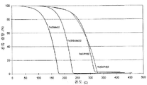
- 238000002411 thermogravimetry Methods 0.000 description 5
- QGZKDVFQNNGYKY-UHFFFAOYSA-N Ammonia Chemical compound N QGZKDVFQNNGYKY-UHFFFAOYSA-N 0.000 description 4
- 125000000217 alkyl group Chemical group 0.000 description 4
- 239000011261 inert gas Substances 0.000 description 4
- 125000001449 isopropyl group Chemical group [H]C([H])([H])C([H])(*)C([H])([H])[H] 0.000 description 4
- 125000004122 cyclic group Chemical group 0.000 description 3
- 238000004519 manufacturing process Methods 0.000 description 3
- 125000000999 tert-butyl group Chemical group [H]C([H])([H])C(*)(C([H])([H])[H])C([H])([H])[H] 0.000 description 3
- TXEYQDLBPFQVAA-UHFFFAOYSA-N tetrafluoromethane Chemical compound FC(F)(F)F TXEYQDLBPFQVAA-UHFFFAOYSA-N 0.000 description 3
- 229910000618 GeSbTe Inorganic materials 0.000 description 2
- KDLHZDBZIXYQEI-UHFFFAOYSA-N Palladium Chemical compound [Pd] KDLHZDBZIXYQEI-UHFFFAOYSA-N 0.000 description 2
- VYPSYNLAJGMNEJ-UHFFFAOYSA-N Silicium dioxide Chemical compound O=[Si]=O VYPSYNLAJGMNEJ-UHFFFAOYSA-N 0.000 description 2
- 229910021529 ammonia Inorganic materials 0.000 description 2
- 230000005587 bubbling Effects 0.000 description 2
- 125000000484 butyl group Chemical group [H]C([*])([H])C([H])([H])C([H])([H])C([H])([H])[H] 0.000 description 2
- 125000006165 cyclic alkyl group Chemical group 0.000 description 2
- PZPGRFITIJYNEJ-UHFFFAOYSA-N disilane Chemical compound [SiH3][SiH3] PZPGRFITIJYNEJ-UHFFFAOYSA-N 0.000 description 2
- 125000001495 ethyl group Chemical group [H]C([H])([H])C([H])([H])* 0.000 description 2
- 230000008020 evaporation Effects 0.000 description 2
- 238000001704 evaporation Methods 0.000 description 2
- 238000010438 heat treatment Methods 0.000 description 2
- 125000002496 methyl group Chemical group [H]C([H])([H])* 0.000 description 2
- 238000012986 modification Methods 0.000 description 2
- 230000004048 modification Effects 0.000 description 2
- BASFCYQUMIYNBI-UHFFFAOYSA-N platinum Chemical compound [Pt] BASFCYQUMIYNBI-UHFFFAOYSA-N 0.000 description 2
- 230000008569 process Effects 0.000 description 2
- 239000004065 semiconductor Substances 0.000 description 2
- 150000004756 silanes Chemical class 0.000 description 2
- VEDJZFSRVVQBIL-UHFFFAOYSA-N trisilane Chemical compound [SiH3][SiH2][SiH3] VEDJZFSRVVQBIL-UHFFFAOYSA-N 0.000 description 2
- WFKWXMTUELFFGS-UHFFFAOYSA-N tungsten Chemical compound [W] WFKWXMTUELFFGS-UHFFFAOYSA-N 0.000 description 2
- 229910052721 tungsten Inorganic materials 0.000 description 2
- 239000010937 tungsten Substances 0.000 description 2
- 238000009834 vaporization Methods 0.000 description 2
- 230000008016 vaporization Effects 0.000 description 2
- UFHFLCQGNIYNRP-UHFFFAOYSA-N Hydrogen Chemical compound [H][H] UFHFLCQGNIYNRP-UHFFFAOYSA-N 0.000 description 1
- 229910052581 Si3N4 Inorganic materials 0.000 description 1
- QVGXLLKOCUKJST-UHFFFAOYSA-N atomic oxygen Chemical compound [O] QVGXLLKOCUKJST-UHFFFAOYSA-N 0.000 description 1
- 230000015572 biosynthetic process Effects 0.000 description 1
- 239000006227 byproduct Substances 0.000 description 1
- 230000015556 catabolic process Effects 0.000 description 1
- 239000005387 chalcogenide glass Substances 0.000 description 1
- 230000008859 change Effects 0.000 description 1
- 238000010276 construction Methods 0.000 description 1
- 125000000113 cyclohexyl group Chemical group [H]C1([H])C([H])([H])C([H])([H])C([H])(*)C([H])([H])C1([H])[H] 0.000 description 1
- 125000001511 cyclopentyl group Chemical group [H]C1([H])C([H])([H])C([H])([H])C([H])(*)C1([H])[H] 0.000 description 1
- 125000001559 cyclopropyl group Chemical group [H]C1([H])C([H])([H])C1([H])* 0.000 description 1
- 238000006731 degradation reaction Methods 0.000 description 1
- 238000004821 distillation Methods 0.000 description 1
- 238000002474 experimental method Methods 0.000 description 1
- 230000006870 function Effects 0.000 description 1
- 125000000524 functional group Chemical group 0.000 description 1
- PCHJSUWPFVWCPO-UHFFFAOYSA-N gold Chemical compound [Au] PCHJSUWPFVWCPO-UHFFFAOYSA-N 0.000 description 1
- 229910052737 gold Inorganic materials 0.000 description 1
- 239000010931 gold Substances 0.000 description 1
- 125000004435 hydrogen atom Chemical group [H]* 0.000 description 1
- 239000012705 liquid precursor Substances 0.000 description 1
- 229910052760 oxygen Inorganic materials 0.000 description 1
- 239000001301 oxygen Substances 0.000 description 1
- 229910052763 palladium Inorganic materials 0.000 description 1
- 238000005240 physical vapour deposition Methods 0.000 description 1
- 238000005268 plasma chemical vapour deposition Methods 0.000 description 1
- 238000000623 plasma-assisted chemical vapour deposition Methods 0.000 description 1
- 229910052697 platinum Inorganic materials 0.000 description 1
- 239000010970 precious metal Substances 0.000 description 1
- 125000001436 propyl group Chemical group [H]C([*])([H])C([H])([H])C([H])([H])[H] 0.000 description 1
- 238000010926 purge Methods 0.000 description 1
- 239000012495 reaction gas Substances 0.000 description 1
- 229910052703 rhodium Inorganic materials 0.000 description 1
- 239000010948 rhodium Substances 0.000 description 1
- MHOVAHRLVXNVSD-UHFFFAOYSA-N rhodium atom Chemical compound [Rh] MHOVAHRLVXNVSD-UHFFFAOYSA-N 0.000 description 1
- 239000000377 silicon dioxide Substances 0.000 description 1
- HQVNEWCFYHHQES-UHFFFAOYSA-N silicon nitride Chemical compound N12[Si]34N5[Si]62N3[Si]51N64 HQVNEWCFYHHQES-UHFFFAOYSA-N 0.000 description 1
- 238000004544 sputter deposition Methods 0.000 description 1
- 238000003786 synthesis reaction Methods 0.000 description 1
- 238000002076 thermal analysis method Methods 0.000 description 1
- 238000002230 thermal chemical vapour deposition Methods 0.000 description 1
Images
Classifications
-
- C—CHEMISTRY; METALLURGY
- C23—COATING METALLIC MATERIAL; COATING MATERIAL WITH METALLIC MATERIAL; CHEMICAL SURFACE TREATMENT; DIFFUSION TREATMENT OF METALLIC MATERIAL; COATING BY VACUUM EVAPORATION, BY SPUTTERING, BY ION IMPLANTATION OR BY CHEMICAL VAPOUR DEPOSITION, IN GENERAL; INHIBITING CORROSION OF METALLIC MATERIAL OR INCRUSTATION IN GENERAL
- C23C—COATING METALLIC MATERIAL; COATING MATERIAL WITH METALLIC MATERIAL; SURFACE TREATMENT OF METALLIC MATERIAL BY DIFFUSION INTO THE SURFACE, BY CHEMICAL CONVERSION OR SUBSTITUTION; COATING BY VACUUM EVAPORATION, BY SPUTTERING, BY ION IMPLANTATION OR BY CHEMICAL VAPOUR DEPOSITION, IN GENERAL
- C23C16/00—Chemical coating by decomposition of gaseous compounds, without leaving reaction products of surface material in the coating, i.e. chemical vapour deposition [CVD] processes
- C23C16/22—Chemical coating by decomposition of gaseous compounds, without leaving reaction products of surface material in the coating, i.e. chemical vapour deposition [CVD] processes characterised by the deposition of inorganic material, other than metallic material
- C23C16/30—Deposition of compounds, mixtures or solid solutions, e.g. borides, carbides, nitrides
- C23C16/305—Sulfides, selenides, or tellurides
- C23C16/306—AII BVI compounds, where A is Zn, Cd or Hg and B is S, Se or Te
-
- C—CHEMISTRY; METALLURGY
- C23—COATING METALLIC MATERIAL; COATING MATERIAL WITH METALLIC MATERIAL; CHEMICAL SURFACE TREATMENT; DIFFUSION TREATMENT OF METALLIC MATERIAL; COATING BY VACUUM EVAPORATION, BY SPUTTERING, BY ION IMPLANTATION OR BY CHEMICAL VAPOUR DEPOSITION, IN GENERAL; INHIBITING CORROSION OF METALLIC MATERIAL OR INCRUSTATION IN GENERAL
- C23C—COATING METALLIC MATERIAL; COATING MATERIAL WITH METALLIC MATERIAL; SURFACE TREATMENT OF METALLIC MATERIAL BY DIFFUSION INTO THE SURFACE, BY CHEMICAL CONVERSION OR SUBSTITUTION; COATING BY VACUUM EVAPORATION, BY SPUTTERING, BY ION IMPLANTATION OR BY CHEMICAL VAPOUR DEPOSITION, IN GENERAL
- C23C16/00—Chemical coating by decomposition of gaseous compounds, without leaving reaction products of surface material in the coating, i.e. chemical vapour deposition [CVD] processes
- C23C16/06—Chemical coating by decomposition of gaseous compounds, without leaving reaction products of surface material in the coating, i.e. chemical vapour deposition [CVD] processes characterised by the deposition of metallic material
- C23C16/16—Chemical coating by decomposition of gaseous compounds, without leaving reaction products of surface material in the coating, i.e. chemical vapour deposition [CVD] processes characterised by the deposition of metallic material from metal carbonyl compounds
-
- C—CHEMISTRY; METALLURGY
- C23—COATING METALLIC MATERIAL; COATING MATERIAL WITH METALLIC MATERIAL; CHEMICAL SURFACE TREATMENT; DIFFUSION TREATMENT OF METALLIC MATERIAL; COATING BY VACUUM EVAPORATION, BY SPUTTERING, BY ION IMPLANTATION OR BY CHEMICAL VAPOUR DEPOSITION, IN GENERAL; INHIBITING CORROSION OF METALLIC MATERIAL OR INCRUSTATION IN GENERAL
- C23C—COATING METALLIC MATERIAL; COATING MATERIAL WITH METALLIC MATERIAL; SURFACE TREATMENT OF METALLIC MATERIAL BY DIFFUSION INTO THE SURFACE, BY CHEMICAL CONVERSION OR SUBSTITUTION; COATING BY VACUUM EVAPORATION, BY SPUTTERING, BY ION IMPLANTATION OR BY CHEMICAL VAPOUR DEPOSITION, IN GENERAL
- C23C16/00—Chemical coating by decomposition of gaseous compounds, without leaving reaction products of surface material in the coating, i.e. chemical vapour deposition [CVD] processes
- C23C16/22—Chemical coating by decomposition of gaseous compounds, without leaving reaction products of surface material in the coating, i.e. chemical vapour deposition [CVD] processes characterised by the deposition of inorganic material, other than metallic material
- C23C16/30—Deposition of compounds, mixtures or solid solutions, e.g. borides, carbides, nitrides
-
- H—ELECTRICITY
- H01—ELECTRIC ELEMENTS
- H01L—SEMICONDUCTOR DEVICES NOT COVERED BY CLASS H10
- H01L21/00—Processes or apparatus adapted for the manufacture or treatment of semiconductor or solid state devices or of parts thereof
- H01L21/02—Manufacture or treatment of semiconductor devices or of parts thereof
- H01L21/02104—Forming layers
- H01L21/02365—Forming inorganic semiconducting materials on a substrate
- H01L21/02612—Formation types
- H01L21/02617—Deposition types
- H01L21/0262—Reduction or decomposition of gaseous compounds, e.g. CVD
Landscapes
- Chemical & Material Sciences (AREA)
- Engineering & Computer Science (AREA)
- Organic Chemistry (AREA)
- Chemical Kinetics & Catalysis (AREA)
- General Chemical & Material Sciences (AREA)
- Materials Engineering (AREA)
- Mechanical Engineering (AREA)
- Metallurgy (AREA)
- Inorganic Chemistry (AREA)
- Physics & Mathematics (AREA)
- Condensed Matter Physics & Semiconductors (AREA)
- General Physics & Mathematics (AREA)
- Manufacturing & Machinery (AREA)
- Computer Hardware Design (AREA)
- Microelectronics & Electronic Packaging (AREA)
- Power Engineering (AREA)
- Chemical Vapour Deposition (AREA)
- Semiconductor Memories (AREA)
Applications Claiming Priority (4)
| Application Number | Priority Date | Filing Date | Title |
|---|---|---|---|
| US5712808P | 2008-05-29 | 2008-05-29 | |
| US61/057,128 | 2008-05-29 | ||
| US12/475,204 US8101237B2 (en) | 2008-05-29 | 2009-05-29 | Tellurium precursors for film deposition |
| US12/475,204 | 2009-05-29 |
Publications (1)
| Publication Number | Publication Date |
|---|---|
| KR20110014160A true KR20110014160A (ko) | 2011-02-10 |
Family
ID=41380625
Family Applications (1)
| Application Number | Title | Priority Date | Filing Date |
|---|---|---|---|
| KR1020107026546A Ceased KR20110014160A (ko) | 2008-05-29 | 2009-05-29 | 필름 증착을 위한 텔루륨 전구체 |
Country Status (6)
| Country | Link |
|---|---|
| US (1) | US8101237B2 (enExample) |
| JP (1) | JP2011522120A (enExample) |
| KR (1) | KR20110014160A (enExample) |
| CN (1) | CN102046838A (enExample) |
| TW (1) | TWI480411B (enExample) |
| WO (1) | WO2010055423A2 (enExample) |
Cited By (3)
| Publication number | Priority date | Publication date | Assignee | Title |
|---|---|---|---|---|
| KR20210142320A (ko) * | 2020-05-18 | 2021-11-25 | 서울대학교산학협력단 | 원자층 증착 공정을 이용한 칼코게나이드계 박막의 형성 방법, 이를 적용한 상변화 물질층의 형성 방법 및 상변화 메모리 소자의 제조 방법 |
| KR20210142321A (ko) * | 2020-05-18 | 2021-11-25 | 서울대학교산학협력단 | 원자층 증착 공정을 이용한 칼코게나이드계 박막의 형성 방법, 이를 이용한 스위칭 소자의 형성 방법 및 메모리 소자의 제조 방법 |
| US12356873B2 (en) | 2020-05-18 | 2025-07-08 | Seoul National University R&DBFoundation | Method of forming chalcogenide-based thin film using atomic layer deposition process, method of forming phase change material layer and switching device, and method of fabricating memory device using the same |
Families Citing this family (21)
| Publication number | Priority date | Publication date | Assignee | Title |
|---|---|---|---|---|
| US8288198B2 (en) | 2006-05-12 | 2012-10-16 | Advanced Technology Materials, Inc. | Low temperature deposition of phase change memory materials |
| EP2511280A1 (en) | 2006-11-02 | 2012-10-17 | Advanced Technology Materials, Inc. | Germanium amidinate complexes useful for CVD/ALD of metal thin films |
| KR101458953B1 (ko) | 2007-10-11 | 2014-11-07 | 삼성전자주식회사 | Ge(Ⅱ)소오스를 사용한 상변화 물질막 형성 방법 및상변화 메모리 소자 제조 방법 |
| US8834968B2 (en) | 2007-10-11 | 2014-09-16 | Samsung Electronics Co., Ltd. | Method of forming phase change material layer using Ge(II) source, and method of fabricating phase change memory device |
| SG178736A1 (en) | 2007-10-31 | 2012-03-29 | Advanced Tech Materials | Amorphous ge/te deposition process |
| US20090215225A1 (en) | 2008-02-24 | 2009-08-27 | Advanced Technology Materials, Inc. | Tellurium compounds useful for deposition of tellurium containing materials |
| US8802194B2 (en) | 2008-05-29 | 2014-08-12 | L'Air Liquide, Société Anonyme pour l'Etude et l'Exploitation des Procédés Georges Claude | Tellurium precursors for film deposition |
| WO2010055423A2 (en) | 2008-05-29 | 2010-05-20 | L'air Liquide - Societe Anonyme Pour I'etude Et I'exploitation Des Procedes Georges Claude | Tellurium precursors for film deposition |
| US8636845B2 (en) | 2008-06-25 | 2014-01-28 | L'Air Liquide, Société Anonyme pour l'Etude et l'Exploitation des Procédés Georges Claude | Metal heterocyclic compounds for deposition of thin films |
| JP2013503849A (ja) | 2009-09-02 | 2013-02-04 | レール・リキード−ソシエテ・アノニム・プール・レテュード・エ・レクスプロワタシオン・デ・プロセデ・ジョルジュ・クロード | ゲルマニウム含有フィルムの堆積のための二ハロゲン化ゲルマニウム(ii)先駆物質 |
| KR20120123126A (ko) | 2010-02-03 | 2012-11-07 | 레르 리키드 쏘시에떼 아노님 뿌르 레?드 에렉스뿔라따시옹 데 프로세데 조르즈 클로드 | 박막 증착용 칼코게나이드-함유 전구체, 그의 제조 방법 및 사용 방법 |
| KR101163046B1 (ko) * | 2010-07-08 | 2012-07-05 | 에스케이하이닉스 주식회사 | 상변화 메모리 소자의 제조 방법 |
| RU2440640C1 (ru) * | 2010-11-10 | 2012-01-20 | Государственное образовательное учреждение высшего профессионального образования Дагестанский государственный университет | Способ получения монокристаллических пленок и слоев теллура |
| US9920077B2 (en) | 2013-09-27 | 2018-03-20 | L'Air Liquide, SociétéAnonyme pour l'Etude et l'Exploitation des Procédés Georges Claude | Amine substituted trisilylamine and tridisilylamine compounds and synthesis methods thereof |
| US9543144B2 (en) * | 2014-12-31 | 2017-01-10 | L'air Liquide, Societe Anonyme Pour L'etude Et L'exploitation Des Procedes Georges Claude | Vapor deposition of chalcogenide-containing films |
| US9777025B2 (en) | 2015-03-30 | 2017-10-03 | L'Air Liquide, Société pour l'Etude et l'Exploitation des Procédés Georges Claude | Si-containing film forming precursors and methods of using the same |
| US11124876B2 (en) | 2015-03-30 | 2021-09-21 | L'Air Liquide, Société Anonyme pour l'Etude et l'Exploitation des Procédés Georges Claude | Si-containing film forming precursors and methods of using the same |
| US10192734B2 (en) | 2016-12-11 | 2019-01-29 | L'Air Liquide, Société Anonyme pour l'Etude et l'Exploration des Procédés Georges Claude | Short inorganic trisilylamine-based polysilazanes for thin film deposition |
| TWI848976B (zh) * | 2018-10-04 | 2024-07-21 | 日商Adeka股份有限公司 | 原子層堆積法用薄膜形成用原料、薄膜形成用原料、薄膜之製造方法及化合物 |
| TWI889746B (zh) | 2020-02-20 | 2025-07-11 | 美商應用材料股份有限公司 | 含碲薄膜之沉積 |
| CN115216748B (zh) * | 2022-09-19 | 2022-12-30 | 中国科学院苏州纳米技术与纳米仿生研究所 | 碲薄膜的制备方法和半导体器件 |
Family Cites Families (46)
| Publication number | Priority date | Publication date | Assignee | Title |
|---|---|---|---|---|
| US3573958A (en) | 1968-05-31 | 1971-04-06 | Francis E Small | Heat sensitive recording sheet |
| SU570239A1 (ru) | 1976-02-12 | 1979-02-10 | Институт химии АН СССР | "Способ получени кристаллических соединений а1у ву14 |
| US4419386A (en) | 1981-09-14 | 1983-12-06 | Gordon Roy G | Non-iridescent glass structures |
| US4377613A (en) | 1981-09-14 | 1983-03-22 | Gordon Roy G | Non-iridescent glass structures |
| DE4214281A1 (de) | 1992-04-30 | 1993-11-04 | Consortium Elektrochem Ind | Verfahren zur herstellung von germaniumdihalogenid-ether-addukten |
| DE4234998C2 (de) | 1992-10-16 | 2000-11-16 | Michael Denk | Cyclische Amide des Siliciums und des Germaniums |
| US5656338A (en) | 1994-12-13 | 1997-08-12 | Gordon; Roy G. | Liquid solution of TiBr4 in Br2 used as a precursor for the chemical vapor deposition of titanium or titanium nitride |
| WO1998016667A1 (en) | 1996-10-16 | 1998-04-23 | The President And Fellows Of Harvard College | Chemical vapor deposition of aluminum oxide |
| KR20010080276A (ko) | 1998-10-21 | 2001-08-22 | 조이스 브린톤 | 알칼리 토금속 함유 물질의 제조를 위한 액체 화합물 |
| KR20010080412A (ko) | 1998-11-12 | 2001-08-22 | 조이스 브린톤 | 향상된 스텝 커버리지를 갖는 확산 장벽 물질 |
| WO2001066816A1 (en) | 2000-03-03 | 2001-09-13 | President And Fellows Of Harvard College | Liquid sources for cvd of group 6 metals and metal compounds |
| US6984591B1 (en) | 2000-04-20 | 2006-01-10 | International Business Machines Corporation | Precursor source mixtures |
| EP1180553A1 (en) | 2000-08-15 | 2002-02-20 | Air Products And Chemicals, Inc. | CVD process for depositing copper on a barrier layer |
| EP1772534A3 (en) | 2000-09-28 | 2007-04-25 | The President and Fellows of Harvard College | Tungsten-containing and hafnium-containing precursors for vapor deposition |
| AU2003228402A1 (en) | 2002-03-28 | 2003-10-13 | President And Fellows Of Harvard College | Vapor deposition of silicon dioxide nanolaminates |
| JP4714422B2 (ja) | 2003-04-05 | 2011-06-29 | ローム・アンド・ハース・エレクトロニック・マテリアルズ,エル.エル.シー. | ゲルマニウムを含有するフィルムを堆積させる方法、及び蒸気送達装置 |
| JP4954448B2 (ja) | 2003-04-05 | 2012-06-13 | ローム・アンド・ハース・エレクトロニック・マテリアルズ,エル.エル.シー. | 有機金属化合物 |
| US7071125B2 (en) | 2004-09-22 | 2006-07-04 | Intel Corporation | Precursors for film formation |
| KR100618879B1 (ko) | 2004-12-27 | 2006-09-01 | 삼성전자주식회사 | 게르마늄 전구체, 이를 이용하여 형성된 gst 박막,상기 박막의 제조 방법 및 상변화 메모리 소자 |
| US20060172068A1 (en) | 2005-01-28 | 2006-08-03 | Ovshinsky Stanford R | Deposition of multilayer structures including layers of germanium and/or germanium alloys |
| US20060172067A1 (en) | 2005-01-28 | 2006-08-03 | Energy Conversion Devices, Inc | Chemical vapor deposition of chalcogenide materials |
| KR100688532B1 (ko) | 2005-02-14 | 2007-03-02 | 삼성전자주식회사 | 텔루르 전구체, 이를 이용하여 제조된 Te-함유 칼코게나이드(chalcogenide) 박막, 상기 박막의 제조방법 및 상변화 메모리 소자 |
| US7678420B2 (en) | 2005-06-22 | 2010-03-16 | Sandisk 3D Llc | Method of depositing germanium films |
| KR100962623B1 (ko) | 2005-09-03 | 2010-06-11 | 삼성전자주식회사 | 상변화 물질층 형성 방법, 이를 이용한 상변화 메모리 유닛및 상변화 메모리 장치의 제조 방법 |
| US8133802B2 (en) | 2005-11-23 | 2012-03-13 | Arizona Board Of Regents | Silicon-germanium hydrides and methods for making and using same |
| WO2007067604A2 (en) | 2005-12-06 | 2007-06-14 | Structured Materials Inc. | Method of making undoped, alloyed and doped chalcogenide films by mocvd processes |
| KR100695168B1 (ko) | 2006-01-10 | 2007-03-14 | 삼성전자주식회사 | 상변화 물질 박막의 형성방법, 이를 이용한 상변화 메모리소자의 제조방법 |
| US8288198B2 (en) | 2006-05-12 | 2012-10-16 | Advanced Technology Materials, Inc. | Low temperature deposition of phase change memory materials |
| US7638645B2 (en) | 2006-06-28 | 2009-12-29 | President And Fellows Of Harvard University | Metal (IV) tetra-amidinate compounds and their use in vapor deposition |
| KR101467587B1 (ko) | 2006-06-28 | 2014-12-01 | 프레지던트 앤드 펠로우즈 오브 하바드 칼리지 | 금속(ⅳ) 테트라-아미디네이트 화합물 및 기상증착에서의 그의 용도 |
| US20080032064A1 (en) | 2006-07-10 | 2008-02-07 | President And Fellows Of Harvard College | Selective sealing of porous dielectric materials |
| KR100757415B1 (ko) | 2006-07-13 | 2007-09-10 | 삼성전자주식회사 | 게르마늄 화합물 및 그 제조 방법, 상기 게르마늄 화합물을이용한 상변화 메모리 장치 및 그 형성 방법 |
| US7547631B2 (en) | 2006-07-31 | 2009-06-16 | Rohm And Haas Electronic Materials Llc | Organometallic compounds |
| US7630142B2 (en) * | 2006-10-20 | 2009-12-08 | Olympus Imaging Corp. | Bent type zoom optical system and imaging system using the same |
| KR100829602B1 (ko) | 2006-10-20 | 2008-05-14 | 삼성전자주식회사 | 상변화 물질층 형성 방법 및 상변화 메모리 장치의 제조방법 |
| EP2511280A1 (en) | 2006-11-02 | 2012-10-17 | Advanced Technology Materials, Inc. | Germanium amidinate complexes useful for CVD/ALD of metal thin films |
| KR100871692B1 (ko) | 2006-11-07 | 2008-12-08 | 삼성전자주식회사 | 저온 증착용 금속 전구체, 그를 사용한 금속 박막 형성방법 및 상변화 메모리 소자 제조 방법 |
| KR101275799B1 (ko) | 2006-11-21 | 2013-06-18 | 삼성전자주식회사 | 저온 증착이 가능한 게르마늄 전구체를 이용한 상변화층형성방법 및 이 방법을 이용한 상변화 메모리 소자의 제조방법 |
| US8377341B2 (en) | 2007-04-24 | 2013-02-19 | Air Products And Chemicals, Inc. | Tellurium (Te) precursors for making phase change memory materials |
| TWI471449B (zh) | 2007-09-17 | 2015-02-01 | Air Liquide | 用於gst膜沈積之碲前驅物 |
| US7960205B2 (en) * | 2007-11-27 | 2011-06-14 | Air Products And Chemicals, Inc. | Tellurium precursors for GST films in an ALD or CVD process |
| US20090162973A1 (en) | 2007-12-21 | 2009-06-25 | Julien Gatineau | Germanium precursors for gst film deposition |
| KR101580575B1 (ko) | 2008-04-25 | 2015-12-28 | 에이에스엠 인터내셔널 엔.브이. | 텔루르와 셀렌 박막의 원자층 증착을 위한 전구체의 합성과 그 용도 |
| US8765223B2 (en) | 2008-05-08 | 2014-07-01 | Air Products And Chemicals, Inc. | Binary and ternary metal chalcogenide materials and method of making and using same |
| WO2010055423A2 (en) | 2008-05-29 | 2010-05-20 | L'air Liquide - Societe Anonyme Pour I'etude Et I'exploitation Des Procedes Georges Claude | Tellurium precursors for film deposition |
| TWM372771U (en) * | 2009-05-20 | 2010-01-21 | Legend Lifestyle Products Corp | Torque detection display device for tool |
-
2009
- 2009-05-29 WO PCT/IB2009/008067 patent/WO2010055423A2/en not_active Ceased
- 2009-05-29 US US12/475,204 patent/US8101237B2/en active Active
- 2009-05-29 KR KR1020107026546A patent/KR20110014160A/ko not_active Ceased
- 2009-05-29 JP JP2011511113A patent/JP2011522120A/ja active Pending
- 2009-05-29 CN CN200980119838XA patent/CN102046838A/zh active Pending
- 2009-06-01 TW TW098118134A patent/TWI480411B/zh not_active IP Right Cessation
Cited By (5)
| Publication number | Priority date | Publication date | Assignee | Title |
|---|---|---|---|---|
| KR20210142320A (ko) * | 2020-05-18 | 2021-11-25 | 서울대학교산학협력단 | 원자층 증착 공정을 이용한 칼코게나이드계 박막의 형성 방법, 이를 적용한 상변화 물질층의 형성 방법 및 상변화 메모리 소자의 제조 방법 |
| KR20210142321A (ko) * | 2020-05-18 | 2021-11-25 | 서울대학교산학협력단 | 원자층 증착 공정을 이용한 칼코게나이드계 박막의 형성 방법, 이를 이용한 스위칭 소자의 형성 방법 및 메모리 소자의 제조 방법 |
| KR20220130061A (ko) * | 2020-05-18 | 2022-09-26 | 서울대학교산학협력단 | 원자층 증착 공정을 이용한 칼코게나이드계 박막의 형성 방법, 이를 적용한 상변화 물질층의 형성 방법 및 상변화 메모리 소자의 제조 방법 |
| KR20220130638A (ko) * | 2020-05-18 | 2022-09-27 | 서울대학교산학협력단 | 원자층 증착 공정을 이용한 칼코게나이드계 박막의 형성 방법, 이를 이용한 스위칭 소자의 형성 방법 및 메모리 소자의 제조 방법 |
| US12356873B2 (en) | 2020-05-18 | 2025-07-08 | Seoul National University R&DBFoundation | Method of forming chalcogenide-based thin film using atomic layer deposition process, method of forming phase change material layer and switching device, and method of fabricating memory device using the same |
Also Published As
| Publication number | Publication date |
|---|---|
| WO2010055423A2 (en) | 2010-05-20 |
| US8101237B2 (en) | 2012-01-24 |
| US20090299084A1 (en) | 2009-12-03 |
| CN102046838A (zh) | 2011-05-04 |
| WO2010055423A3 (en) | 2010-07-15 |
| TWI480411B (zh) | 2015-04-11 |
| JP2011522120A (ja) | 2011-07-28 |
| TW201016877A (en) | 2010-05-01 |
| WO2010055423A8 (en) | 2010-09-02 |
Similar Documents
| Publication | Publication Date | Title |
|---|---|---|
| US8101237B2 (en) | Tellurium precursors for film deposition | |
| KR100956210B1 (ko) | 금속 실리콘 질화물 박막의 플라즈마 강화 사이클릭증착방법 | |
| US8454928B2 (en) | Tellurium precursors for GST deposition | |
| US8318252B2 (en) | Antimony precursors for GST films in ALD/CVD processes | |
| US8691668B2 (en) | Dihalide germanium(II) precursors for germanium-containing film depositions | |
| US8193388B2 (en) | Compounds for depositing tellurium-containing films | |
| US20090162973A1 (en) | Germanium precursors for gst film deposition | |
| KR101499260B1 (ko) | 상 변화 메모리 재료의 저온 증착 | |
| JP5275243B2 (ja) | 新規なv族金属含有前駆体および金属含有膜の堆積のためのその使用 | |
| US9103019B2 (en) | Metal precursors containing beta-diketiminato ligands | |
| US9240319B2 (en) | Chalcogenide-containing precursors, methods of making, and methods of using the same for thin film deposition | |
| US8357614B2 (en) | Ruthenium-containing precursors for CVD and ALD | |
| US20110262660A1 (en) | Chalcogenide-containing precursors, methods of making, and methods of using the same for thin film deposition | |
| US8802194B2 (en) | Tellurium precursors for film deposition | |
| EP2492273A1 (en) | Deposition of gallium containing thin films using gallium alkylamide precursor | |
| EP2492272A1 (en) | Deposition of indium containing thin films using indium alkylamide precursor | |
| EP2540733A1 (en) | Deposition of indium containing thin films using new indium precursors | |
| EP2540732A1 (en) | Deposition of gallium containing thin films using new gallium precursors. |
Legal Events
| Date | Code | Title | Description |
|---|---|---|---|
| PA0105 | International application |
Patent event date: 20101126 Patent event code: PA01051R01D Comment text: International Patent Application |
|
| PG1501 | Laying open of application | ||
| A201 | Request for examination | ||
| PA0201 | Request for examination |
Patent event code: PA02012R01D Patent event date: 20140527 Comment text: Request for Examination of Application |
|
| E902 | Notification of reason for refusal | ||
| PE0902 | Notice of grounds for rejection |
Comment text: Notification of reason for refusal Patent event date: 20150922 Patent event code: PE09021S01D |
|
| E902 | Notification of reason for refusal | ||
| PE0902 | Notice of grounds for rejection |
Comment text: Notification of reason for refusal Patent event date: 20151230 Patent event code: PE09021S01D |
|
| E601 | Decision to refuse application | ||
| PE0601 | Decision on rejection of patent |
Patent event date: 20160616 Comment text: Decision to Refuse Application Patent event code: PE06012S01D Patent event date: 20151230 Comment text: Notification of reason for refusal Patent event code: PE06011S01I Patent event date: 20150922 Comment text: Notification of reason for refusal Patent event code: PE06011S01I |