KR20100131490A - Programmable gain trans-impedance amplifier overload recovery circuit - Google Patents
Programmable gain trans-impedance amplifier overload recovery circuit Download PDFInfo
- Publication number
- KR20100131490A KR20100131490A KR1020107023169A KR20107023169A KR20100131490A KR 20100131490 A KR20100131490 A KR 20100131490A KR 1020107023169 A KR1020107023169 A KR 1020107023169A KR 20107023169 A KR20107023169 A KR 20107023169A KR 20100131490 A KR20100131490 A KR 20100131490A
- Authority
- KR
- South Korea
- Prior art keywords
- stage amplifier
- output
- amplifier
- value
- inverting input
- Prior art date
Links
Images


Classifications
-
- G—PHYSICS
- G01—MEASURING; TESTING
- G01R—MEASURING ELECTRIC VARIABLES; MEASURING MAGNETIC VARIABLES
- G01R31/00—Arrangements for testing electric properties; Arrangements for locating electric faults; Arrangements for electrical testing characterised by what is being tested not provided for elsewhere
- G01R31/50—Testing of electric apparatus, lines, cables or components for short-circuits, continuity, leakage current or incorrect line connections
- G01R31/64—Testing of capacitors
-
- G—PHYSICS
- G01—MEASURING; TESTING
- G01R—MEASURING ELECTRIC VARIABLES; MEASURING MAGNETIC VARIABLES
- G01R19/00—Arrangements for measuring currents or voltages or for indicating presence or sign thereof
- G01R19/0092—Arrangements for measuring currents or voltages or for indicating presence or sign thereof measuring current only
Abstract
용량성 컴포넌트의 누설 전류를 측정하기 위한 장치의 실시예가 교시된다. 일 실시예는 반전 입력에서 직렬 접속된 용량성 컴포넌트로부터의 입력을 수신하도록 구성되는 제1 단 증폭기와, 제1 단 증폭기의 피드백 경로에 있는 피드백 저항기를 포함한다. 피드백 저항기의 저항값은 누설 전류의 예상 값과 대응하는 전압 출력에 기초하여 프로그래밍 가능하다. Embodiments of an apparatus for measuring leakage current of a capacitive component are taught. One embodiment includes a first stage amplifier configured to receive input from a capacitive component connected in series at an inverting input, and a feedback resistor in the feedback path of the first stage amplifier. The resistance value of the feedback resistor is programmable based on the voltage output corresponding to the expected value of the leakage current.

Description
본 발명은 일반적으로 용량성 컴포넌트(capacitive component)에 대한 테스트에 관한 것이다. The present invention generally relates to testing for capacitive components.
커패시터와 같은 용량성 컴포넌트를 테스트하기 위한 공지된 장치 및 방법에서는 컴포넌트가 먼저 원하는 전압으로 대전된다. 그 다음, 누설 전류(leakage current)가 측정된다. 누설 전류에 대하여 범위를 벗어나는 값은 컴포넌트에 결함이 있다는 것을 나타낼 수 있다. In known apparatus and methods for testing capacitive components, such as capacitors, the components are first charged to a desired voltage. Then, leakage current is measured. Values out of range for leakage current may indicate that a component is defective.
본 발명은 프로그래밍 가능한 이득 트랜스 임피던스(trans-impedance) 증폭기 과부하 복구(overload recovery) 회로를 제공하고자 한다. The present invention seeks to provide a programmable gain trans-impedance amplifier overload recovery circuit.
본 발명의 실시예는 용량성 컴포넌트의 테스트 속도를 높일 방식을 제공하며, 이는 특히 자동화된 대량 제조 공정에 바람직하다. 구체적으로, 본 발명은 원하는 테스트를 수행하기 위하여 과부하로부터 빠르게 복구하는 장치의 실시예를 제공한다. Embodiments of the present invention provide a way to speed up testing of capacitive components, which is particularly desirable for automated mass manufacturing processes. In particular, the present invention provides an embodiment of an apparatus for quickly recovering from an overload to perform a desired test.
특정 실시예의 본 발명의 특징이 아래에서 보다 상세하게 기재된다. Features of the invention in certain embodiments are described in more detail below.
본 발명에 따르면 프로그래밍 가능한 이득 트랜스 임피던스 증폭기 과부하 복구 회로를 제공할 수 있다. According to the present invention, a programmable gain transimpedance amplifier overload recovery circuit can be provided.
본 명세서에서의 설명은 첨부 도면을 참조하여 이루어지며, 유사한 참조 번호는 여러 도면들에 걸쳐 유사한 부분들을 칭한다.
도 1은 본 발명의 하나의 실시예에 따른 트랜스 임피던스 증폭기의 개략도이다.
도 2는 본 발명의 다른 실시예에 따른 트랜스 임피던스 증폭기의 개략도이다.
도 3은 본 발명의 또 다른 실시예에 따른 트랜스 임피던스 증폭기의 개략도이다.
도 4는 각 단(stage)의 프로그래밍 가능한 이득을 도시하는 도 3에 따른 트랜스 임피던스 증폭기의 개략도이다.
도 5는 본 발명의 실시예가 사용될 수 있는 전자 컴포넌트 처리 기계의 평면도이다.
도 6은 도 1에 따른 트랜스 임피던스 증폭기와 통합된 고속 복구 전류 싱크의 개략도이다. The description herein is made with reference to the accompanying drawings, wherein like reference numerals refer to similar parts throughout the several views.
1 is a schematic diagram of a transimpedance amplifier in accordance with one embodiment of the present invention.
2 is a schematic diagram of a transimpedance amplifier according to another embodiment of the present invention.
3 is a schematic diagram of a transimpedance amplifier according to another embodiment of the present invention.
4 is a schematic diagram of a transimpedance amplifier according to FIG. 3 showing the programmable gain of each stage.
5 is a plan view of an electronic component processing machine in which an embodiment of the present invention may be used.
6 is a schematic diagram of a fast recovery current sink integrated with the transimpedance amplifier according to FIG. 1.
누설 전류에 대하여 다층 세라믹 커패시터(MLCC; multi-layer ceramic capacitor)와 같은 용량성 컴포넌트를 테스트할 때, 대부분의 통과된 전류가 대전 다이오드로 빠지는 경우, 대전 전류의 일부를 감지 회로로 전달하는 대전되지 않은 용량성 컴포넌트로 인해 감지 회로가 견디는 큰 전류가 존재한다. 이상적으로, 용량성 컴포넌트는 완전히 대전되면 더 이상 전류를 통과시키지 않는다. 실제로는 누설 전류가 통과하며, 이 전류의 정확한 측정이 용량성 컴포넌트의 품질, 구체적으로 절연 저항의 중요한 측정이다. When testing capacitive components such as multi-layer ceramic capacitors (MLCCs) for leakage current, if most of the current passed through the charge diode is uncharged, it transfers a portion of the charge current to the sensing circuit. Due to the non-capacitive components, there is a large current that the sense circuit withstands. Ideally, the capacitive component no longer passes current when fully charged. In practice, leakage current passes through, and accurate measurement of this current is an important measure of the quality of the capacitive components, specifically the insulation resistance.
종래에, 이러한 테스트는 각각의 이득을 갖는 하나 이상의 연산 증폭기(op amp)를 포함하는 회로를 사용하여 수행된다. op amp에 대하여, op amp가 포화 상태(saturation)로 들어가기 전에 그의 입력 신호가 소정의 구성에서 얼마나 클 수 있는지에 대한 한정된 제한이 있다. op amp가 포화 상태에 있을 때, op amp가 그의 동작 범위 내에 있는 점으로 입력 신호가 감소되고 올바른 출력 신호를 제공할 수 있을 때까지, op amp의 출력은 그의 양 또는 음의 공급 전압으로 고정된다. op amp가 포화 상태에서 얼마나 빨리 나올 수 있는지는, 그의 출력 전류 소싱 성능, 구성 및 로딩을 포함하지만 이에 한정되는 것은 아닌 여러 요인들의 함수이다. 회로가 하나보다 많은 수의 op amp를 포함할 때, 출력을 포화 상태로 야기한 제1 단 op amp의 입력에서의 과부하는 다음 단도 포화 상태로 넣을 수 있다. Traditionally, such tests are performed using circuitry that includes one or more op amps with respective gains. For an op amp, there is a finite limit on how large its input signal can be in a given configuration before the op amp enters saturation. When the op amp is in saturation, the output of the op amp is held at its positive or negative supply voltage until the input signal is reduced to the point that the op amp is within its operating range and can provide the correct output signal. . How quickly an op amp can come out of saturation is a function of several factors, including but not limited to its output current sourcing performance, configuration and loading. When the circuit contains more than one op amp, the overload at the input of the first stage op amp that caused the output to saturate can enter the next stage of saturation.
데이터 획득을 테스트할 때 그리고 속도가 중요한 경우에, 주어진 시간에 정확한 데이터를 얻을 수 있도록 그리고/또는 다음 데이터 세트를 빠르게 획득할 수 있도록, 과부하 상태로부터의 빠른 복구가 바람직하다. 따라서, 본 명세서에 기재되어 있는 본 발명의 실시예는 이러한 과부하를 벗어나도록 측정 회로를 능동으로 구동한다. When testing data acquisition and where speed is important, fast recovery from overload is desirable to obtain accurate data at a given time and / or to quickly acquire the next data set. Thus, embodiments of the invention described herein actively drive the measurement circuitry to overcome this overload.
도 1은 본 발명의 하나의 실시예에 따른 트랜스 임피던스 증폭기를 도시한다. 도 1은 일정한 전류 Iin를 제공하는 전류 소스(10)를 포함한다. 전류 소스(10)는 원하는 출력 값이 주어지면 당해 분야에서의 지식 내에서 임의의 수의 회로 설계에 의해 구현될 수 있다. 예를 들어, 전류 소스(10)는 공동 양도된 미국 특허 공보 제2008/0290879 A1호에 기재된 바와 같이 프로그래밍 가능한 전류 소스에 연결된 가변 전압을 공급하는 전압 소스의 조합을 나타낼 수 있으며, 상기 특허는 참조에 의해 그 전체가 본 명세서에 포함된다. 1 illustrates a transimpedance amplifier according to one embodiment of the invention. 1 includes a
도 1에서, 테스트될 용량성 컴포넌트, 이하 DUT(device under test)(20)가 점선으로 도시되어 있다. 이후에 추가적으로 상세하게 설명되는 바와 같이, 다수의 이러한 디바이스들은 전류 소스(10) 및 트랜스 임피던스 증폭기를 포함하는 측정 회로에 접속되면 순차적으로 테스트된다. In FIG. 1, the capacitive component to be tested, hereinafter device under test (DUT) 20, is shown in dashed lines. As will be described in further detail below, many such devices are tested sequentially when connected to a measurement circuit comprising a
DUT(20)는 전류 소스(10)에 직렬로 연결되며, 그를 통과하는 전류가 저항기(14)를 통하여 전류 감지 증폭기(12)로서 구성된 op amp의 반전 입력에 공급된다. 전류 감지 증폭기(12)의 비반전 입력은 접지된다. Vout으로부터의 전류 감지 증폭기(12)의 반전 입력에의 피드백이 저항기(16)에 의해 커패시터(18)와 병렬로 제공된다. 저항기(16)의 값은 Rf이다. The
전류 감지 증폭기(12)의 전달 함수는 Vout = -Iin*Rf이며, 이는 주어진 입력 전류에 대하여, 출력 전압 Vout이 입력 전류와 저항 값 Rf의 수학적 곱임을 의미한다. Rf의 오믹 값은 설계 요건에 기초하여 선택된다. 예를 들어, 측정된 누설 전류가 +/-1mA 사이의 값이라 하면 Vout에서 풀 스케일(full scale)은 +/-5V를 나타낸다. 5㏀의 Rf의 값이 사용될 수 있다. 풀 스케일은 설계자에 의해 애플리케이션에 기초하여 정의된다. Rf의 값의 프로그래밍은 도 4에 관련하여 이후에 보다 상세하게 설명된다. The transfer function of the
도 2는 제1 단으로서 도 1의 전류 감지 증폭기(12)를 가지며 비반전 전압 증폭기(22)로서 구성된 op amp 형태의 비반전 이득 단이 추가된 트랜스 임피던스 증폭기를 포함한다. 저레벨 신호를 모니터하려고 할 때 도 2에서 보이는 바와 같은 하나 이상의 추가적인 이득 단이 필요할 수 있다. 이어서 제1 증폭기에서 Rf의 값을 증가시킬 수 있다. 그러나, 본 발명자는 전류 감지 증폭기(12)의 op amp가 이득 또는 대역폭에 대한 그의 한계에 도달한다면 이러한 해결책이 문제가 될 수 있다는 것을 발견하였다. 또한, 어떤 환경에서는, Rf의 오믹 값을 더 작게 유지하는 것이 시스템의 잡음 이득을 도울 수 있다. 제2 단 비반전 전압 증폭기에 의해 제공된 추가적인 증폭기는 앞서 기재한 제1 단에 대해 범위 및 풀 스케일 값을 결정하는데 동일한 로직의 적용을 가능하게 한다. FIG. 2 includes a transimpedance amplifier having the
도 2에서, 제1 단의 출력, 전압 Vin은 전압 증폭기(22)의 비반전 입력에 제공된다. 전압 증폭기(22)의 출력으로부터 그의 반전 입력으로의 피드백은 R3의 저항 값을 갖는 저항기(24)를 통하여 제공되며, 반전 입력은 R2의 저항 값을 갖는 저항기(26)를 통하여 접지된다. 이 이득 단의 전달 함수는 Vout = Vin*(1+R3/R2)이다. 앞서 기재한 바와 같이 그리고 제1 단의 출력이 Vin인 경우에, 제1 단의 전달 함수는 Vin = -Iin*Rf이다. 따라서, 알고 있는 전류 Iin과 원하는 최대 입력 전압 Vin 및 원하는 최대 출력 전압 Vout을 이용해, Rf, R3 및 R2에 대하여 적합한 값을 할당할 수 있다. 예를 들어 측정될 누설 전류가 (상기 예에서와 같은 +/-1 mA 대신에) +/-1 ㎂ 사이에 속하는 것으로 예상되며 풀 스케일이 +/-5V를 나타내는 경우에, 제2 단의 이득 (1+R3/R2)이 4인 경우, Rf의 오믹 값은 1.25 ㏁이다. In Fig. 2, the output of the first stage, the voltage Vin, is provided to the non-inverting input of the
제2 단이 비반전 전압 증폭기(22)로서 도시되어 있지만, op amp는 그 대신에 도 4에 관련하여 아래에 보다 상세하게 기재되어 있는 바와 같이 비반전 단위 이득(unity gain) 버퍼로서 구성될 수 있다. 또한, 본 명세서에서의 교시에 기초하여, 원하는 경우 하나보다 많은 수의 증폭 단이 포함될 수 있다. Although the second stage is shown as a
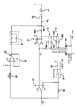
도 3은 도 2에 도시된 제1 및 제2 단을 포함하고, 제2 단의 출력으로부터 제1 단의 반전 입력으로의 추가적인 피드백 회로를 추가한다. 도 3에 도시된 바와 같이, 제2 비반전 이득단의 전압 증폭기(22)의 출력은 2개의 백투백(back-to-back) 제너 다이오드(Zener diode)(28)에 접속된다. 제너 다이오드(28)는 저항기(30)를 통하여 접지에 직렬 접속된다. 비반전 버퍼(32)로서 구성된 op amp는 제너 다이오드(28)에 이어진다. 즉, 제너 다이오드(28)는 버퍼(32)의 비반전 입력에 연결되고, 피드백 경로(34)가 버퍼(32)의 출력과 그의 반전 입력 사이에 제공된다. 버퍼(32)의 출력은 백투백 신호 다이오드(36)에 접속되며, 이는 이어서 제1 단의 전류 감지 증폭기(12)의 반전 입력에 연결된다. 보다 구체적으로, 도 1 및 도 2의 저항기(14)는 도 3의 저항기(14a 및 14b)로 교체되고, 백투백 제너 다이오드(28), 비반전 버퍼(32) 및 백투백 신호 다이오드(36)에 의해 제공되는 피드백 회로는 저항기(14a과 14b) 사이의 노드(38)에 접속된다. 3 includes the first and second stages shown in FIG. 2 and adds additional feedback circuits from the output of the second stage to the inverting input of the first stage. As shown in FIG. 3, the output of the
이 회로에서, 바람직한 예상 범위 내의 입력 전류는 앞서 설명한 바와 같이 회로가 단들의 전달 함수에 의해 결정되는 선형 방식으로 거동할 수 있게 해준다. 정상적인 동작 동안, 백투백 제너 다이오드(28)는 피드백 경로로의 전류 흐름을 막는데, Vout이 제너 다이오드의 턴온(turn on) 전압보다 낮기 때문이다. 비반전 버퍼(32)는 비활성이며, 백투백 신호 다이오드(36)는 노드(38)로부터 비반전 버퍼(32)의 출력으로의 전류 흐름을 막는다. 그러나, 회로로 들어가는 입력 전류(즉, 제1 단 전류 감지 증폭기(12)의 반전 입력으로의 입력 전류)가 범위 밖이고 그의 레일 중 어느 하나로 증폭기의 출력을 구동시키기에 충분히 큰 경우에, 전압 증폭기(22)로부터의 전압 출력 Vout은 그의 전력 공급 레일을 향하여 이동하기 시작한다. 제너 다이오드(28)를 턴온할 만큼 충분히 크다면, Vout은 제너 다이오드(28)의 클램핑 전압(clamping voltage)에 있을 것이다. 그러면, 클램핑 전압이 비반전 버퍼(32)에 제공되며, 이는 바람직하게 고전류 구동 용량에 대하여 선택된다. 버퍼(32)의 출력으로부터의 전류가 신호 다이오드에 공급되고, 신호 다이오드는 버퍼(32)로부터의 충분한 전류가 그들에 공급된 후에 전도하기 시작하며, 이어서 노드(38)에서의 포텐셜을 더 낮게 능동으로 구동시킨다. 이 포텐셜이 낮아짐에 따라, 전류 감지 증폭기(12)가 보는 입력 신호는 증폭기가 그 입력에서의 과부하로부터의 복구를 시작할 수 있게 해주도록 감소된다. In this circuit, the input current within the desired expected range allows the circuit to behave in a linear manner determined by the transfer function of the stages as described above. During normal operation, the back-to-
도 3은 제2 단의 출력으로부터 제1 단의 반전 입력으로의 피드백 회로를 도시하지만, 도 3의 피드백 회로는 도 1에서 교시된 바와 같이 단일 단으로 구현될 수 있다. 이는 적어도 안정화 이유를 위해 일반적으로 덜 바람직하지만, 가능하다. 또한, 도 3의 구성은 도 2의 비반전 증폭기(22)가 도 4에 관련하여 기재된 버퍼로 교체되는 것으로 구현될 수 있다. Although FIG. 3 shows a feedback circuit from the output of the second stage to the inverting input of the first stage, the feedback circuit of FIG. 3 may be implemented in a single stage as taught in FIG. This is generally less desirable, but at least for reasons of stabilization. In addition, the configuration of FIG. 3 may be implemented such that the
회로 토폴로지에서의 이득은 도 4에 도시된 바와 같이 프로그래밍 가능할 수 있다. 도 4에서, 제1 단과 제2 단 둘 다의 이득은 애플리케이션에 따라 프로그래밍 가능하다. 도 3에 도시된 구성에 더하여, 도 4는 전류 감지 증폭기(12)에 대한 2개의 피드백 회로에 연결된 FPGA(field-programmable gate array)(50)를 포함한다. 보다 구체적으로, 제1 피드백 회로(52)는 병렬로 구성된 저항기(16a)와 커패시터(18a)를 포함하고, 제2 피드백 회로(54)는 병렬로 구성된 저항기(16b)와 커패시터(18b)를 포함한다. 저항기(16)에 관련하여 앞서 기재한 바와 같이, 16a나 16b의 값은 Rf이다. 둘보다 많은 수의 피드백 회로가 가능하다. FPGA(50)는 제어 신호 1 및 2에 따라 제1 또는 제2 피드백 회로(52, 54) 중 어느 하나로 전환하도록, 즉 인에이블하도록 프로그래밍된다. 마찬가지로, 비반전 전압 증폭기(22)의 저항기(26)에 연결된 스위치(56)에 대하여 선택적 제어가 제공된다. 스위치(56)로의 제어 신호 3의 인가를 통해, 저항기(26)(값 R2를 가짐)는 회로의 안팎으로 전환될 수 있다. 당해 기술 분야에서의 숙련자라면 이러한 설명으로부터 알 수 있듯이, 저항기(26)를 생략한다면 op amp의 구성을 비반전 전압 증폭기(22)의 것으로부터 비반전 단위 이득 버퍼로 변경할 것이다. 이 구성은 출력 신호 Vin이 증폭될 필요가 없을 때 유용하다. 도 3의 설명에서와 같이, 제2 단은 원하는 경우 그 전체가 생략될 수 있다. The gain in the circuit topology may be programmable as shown in FIG. 4. In Figure 4, the gain of both the first stage and the second stage is programmable according to the application. In addition to the configuration shown in FIG. 3, FIG. 4 includes a field-programmable gate array (FPGA) 50 coupled to two feedback circuits for the
이 실시예에서의 제어 신호 1, 2, 및 3은 다양한 입력 및 출력 접속 이외에도, RAM, ROM, KAM(keep alive memory), CPU 등을 포함하는 마이크로컴퓨터에 의해 제공된다. 도 5에 관련하여 아래에 기재된 응용예에서, 예를 들어, 마이크로컴퓨터는 용량성 컴포넌트의 크기에 따라 달라지는 예상되는 누설 전류, 및 대응하는 풀 스케일 전압와 같은 정보를 포함한 사용자에 의한 셋업 메뉴의 제시를 포함하여 기재된 테스트를 수행하도록 소프트웨어 프로그램을 동작시킨다. 이 메뉴에 응답하여, 마이크로컴퓨터는 FPGA(50) 및 스위치(56)에 제공된 제어 신호 1, 2, 및 3을 통해 이득을 프로그래밍할 수 있다. 물론, FPGA(50)의 함수는 하나 이상의 하드웨어 컴포넌트에 의해 구현될 수 있다. 임의의 수의 고체 상태 스위치가 스위치(56)를 구현하는데 사용될 수 있다. Control signals 1, 2, and 3 in this embodiment are provided by a microcomputer including RAM, ROM, keep alive memory (KAM), CPU, and the like, in addition to various input and output connections. In the application described below with respect to FIG. 5, for example, the microcomputer may present a setup menu by the user that includes information such as the expected leakage current that depends on the size of the capacitive component, and the corresponding full scale voltage. Operating the software program to perform the described tests. In response to this menu, the microcomputer can program the gain through control signals 1, 2, and 3 provided to the
회로 토폴로지에서 프로그래밍 가능한 이득을 갖는 것은, 회로를 포함한 임의의 계측기(meter)가 큰 동적 범위를 가질 수 있게 해준다. 예를 들어, 측정 성능은 +/-200pA까지 내려간 분해능으로써 +/-1mA 사이에서의 누설 전류 값으로부터의 범위일 수 있다. 이 작업은 이러한 정확도 측정이 필요할 때 Rf, R3 및 R2의 고정된 값만을 사용하여 달성하기가 어렵다. 이 범위를 복수의 영역들로 나누는 것은 수반된 하드웨어에 대하여 작업을 더욱 쉽게 한다. 이들 범위 내에서, Rf, R3과 R2에 대한 오믹 값은 상기 기재한 바와 같이 제2 단에 대한 이득 값 및 각각의 범위에 대한 풀 스케일 전압을 정의함으로써 할당될 수 있다. 장비에 대하여 큰 동적 범위가 필요할 때, 전류 감지 증폭기(12)의 Rf의 오믹 값과 증폭기(22)의 이득이 바람직하게 프로그래밍된다. 그러면, 범위와는 독립적으로, 회로로의 입력 전류가 전류 감지 증폭기(12)에서의 과부하를 야기할 만큼 충분히 큰 경우, 증폭기(22)의 출력의 구동은 제너 다이오드(28) 턴온 전압을 향한다. 그 전압에 도달하면, 피드백 네트워크가 활성화되고, 증폭기(12 또는 22)가 자체적으로 할 수 있는 것보다 훨씬 더 빨리 회로가 자신의 선형 범위로 돌아가는 것을 도우며, 전류 감지 증폭기(12)의 출력 전압과 증폭기(22)의 이득의 곱이 제너 다이오드 턴온 전압보다 낮으면 턴 오프된다. 회로는 다시 자신의 선형 범위에 있게 된다. Having a programmable gain in a circuit topology allows any meter, including the circuit, to have a large dynamic range. For example, measurement performance may range from leakage current values between +/- 1 mA with resolutions down to +/- 200 pA. This task is difficult to achieve using only fixed values of Rf, R3 and R2 when such accuracy measurements are needed. Dividing this range into multiple regions makes it easier to work with the hardware involved. Within these ranges, the ohmic values for Rf, R3 and R2 can be assigned by defining the gain value for the second stage and the full scale voltage for each range, as described above. When a large dynamic range is needed for the equipment, the ohmic value of Rf of the
언급한 바와 같이, 누설 전류 값의 범위가 예상될 때, 범위들을 나누고 각 범위에 기초하여 프로그래밍 가능한 이득을 제어하는 것이 바람직하다. 다음의 표는 본 발명의 프로그래밍 가능한 이득 교시를 적용한 예로서 누설 전류의 네 개의 상이한 범위에 대한 값을 제공한다. As mentioned, when a range of leakage current values is expected, it is desirable to divide the ranges and to control the programmable gain based on each range. The following table provides values for four different ranges of leakage current as an example of applying the programmable gain teachings of the present invention.
이들 범위는 도 4의 실시예에서 324 ㏀의 값 Rf를 저항기(16a)와 연관시키고 20 ㏀의 값 Rf를 저항기(16b)와 연관시킴으로써 구현될 수 있다. 그러면 이들 값은 FPGA(50)에 의해 선택적으로 전환될 수 있다. 저항기(24 및 26)의 저항 값은 이득이 4이도록, 예를 들어 값 R3이 3㏀이며 R2의 값이 1㏀일 수 있도록, 설정될 것이다. 그러면 증폭기(22)의 이득은 원하는 범위에 따라 스위치(56)에 의해 1과 4 사이에 이득을 변경하도록 선택적으로 전환될 수 있다. These ranges can be implemented in the embodiment of FIG. 4 by associating a value Rf of 324 μs with a
도 1 내지 도 4 중 임의의 도면에 따른 회로는 용량성 컴포넌트를 테스트하기 위해 임의의 수의 애플리케이션에서 단독형 테스트 디바이스의 일부로서 구현될 수 있다. 트랜스 임피던스 증폭기는 또한 전류 소스와 별도의 디바이스에서 구현될 수 있다. 그러면, 전류 소스는 본 특허 출원의 양수인인 Electro Scientific Industries, Inc.(Portland, OR)로부터 입수가능한 54XX 전원의 모델과 같은 임의의 프로그래밍 가능한 컴퓨터 제어된 소스일 수 있다. 트랜스 임피던스 증폭기의 하나의 특히 바람직한 사용은 비교적 짧은 기간에 대량의 전자 컴포넌트들을 테스트하는 전자 컴포넌트 핸들러에 있다. 이들 핸들러는 Model 3500으로서 판매되는 대량 MLCC 테스터를 포함하지만 이에 한정되는 것은 아닌 다양한 전자 컴포넌트 핸들러를 판매하는 Electro Scientific Industries, Inc.에 의해 시판되는 제품을 포함하지만 이에 한정되지는 않는다. The circuit according to any of FIGS. 1-4 can be implemented as part of a standalone test device in any number of applications for testing capacitive components. The transimpedance amplifier can also be implemented in a device separate from the current source. The current source can then be any programmable computer controlled source, such as a model of a 54XX power supply available from Electro Scientific Industries, Inc. (Portland, OR), the assignee of the present patent application. One particularly preferred use of the transimpedance amplifier is in an electronic component handler that tests a large amount of electronic components in a relatively short period of time. These handlers include, but are not limited to, products marketed by Electro Scientific Industries, Inc., which sell a variety of electronic component handlers, including but not limited to bulk MLCC testers sold as Model 3500.
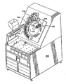
하나의 전자 컴포넌트 처리 기계는 발명의 명칭이 전기 회로 컴포넌트 핸들러(Electrical Circuit Component Handler)인 공동 양도된 미국 특허 출원 번호 제5,842,579호에 예시되어 있으며, 이는 참조에 의해 그 전체가 본 명세서에 포함된다. 도 5는 전기 회로 컴포넌트 핸들러(100)의 전반적인 도면을 도시한다. 핸들러(100)는 로딩 존(130)을 정의하는 로딩 프레임(112), 테스트 존(115)을 정의하는 복수의 테스트 모듈(114), 및 블로우 오프(blow off) 존(170)을 정의하는 블로우 오프(160)를 갖는다. 동작시, 전자 컴포넌트는 진공의 도움으로 테스트 플레이트(그 전체가 도시되지 않음) 상에 발견되는 테스트 자리(124)로 개별적으로 인입되도록 로딩 존(130)에서 로딩 프레임(112)을 통하여 통과된다. 테스트 존(115)에서 컴포넌트를 테스트한 후에, 컴포넌트는 블로우 오프 존(170)으로 이동하며, 여기에서 블로우 오프(160)는 진공을 제거하고 테스트(들)의 결과에 기초하여 부품들을 분류한다. One electronic component processing machine is illustrated in commonly assigned US Patent Application No. 5,842,579, entitled Electrical Circuit Component Handler, which is incorporated herein by reference in its entirety. 5 shows an overall view of the electrical
상세하게 도시되지 않았지만, 본 발명의 실시예와 전류 소스(10)는, 개별적으로 구현된다면, 테스트 존(115)에서 각각의 컴포넌트를 테스트하기 위해 테스트 모듈(114)에 전기 연결될 것이다. 즉, 테스트 자리(124)에서 컴포넌트들은 테스트 모듈(114)의 사용을 통해 테스트 존(115)에서 다수의 테스트를 받게 된다. 예를 들어, MLCC가 테스트될 경우, 예를 들어 커패시턴스, 손실 계수 및 절연 저항에 대한 데이터가 일반적으로 제공된다. 그 다음, 테스트로부터 얻은 데이터를 사용하여 허용오차에 의해 부품들을 분류하고 결함이 있는 부품들을 찾을 수 있다. Although not shown in detail, embodiments of the present invention and
상기에 간략하게 설명한 바와 같이, 동작시, 대전되지 않은 커패시터가 테스트를 위해 들어가며, 여기에서는 테스트 자리(124)에 배치될 때, 대전 전류 및 대전 전압이 이 DUT(20)에 인가되어 개별 제조자 요건에 따라 순서에 맞추어 테스트를 순차적으로 수행한다. 절연 저항(IR) 테스트에 관련하여, 전류 소스(10)로부터 DUT(20)에의 대전 전류의 인가로 인해 전류가 커지게 되며, 트랜스 임피던스 증폭기에서 과부하를 생성하고 전류 감지 증폭기(10)의 과부하가 시작된다. DUT(20)가 대전됨에 따라, 전류 감지 증폭기(12)의 반전 입력에서 보이는 전류가 낮아지기 시작한다. 짧은 시간 후에, 전류 감지 증폭기(12)에의 입력이 누설 전류이다. 측정된 누설 전류는 DUT(20)의 절연 저항을 나타낸다. 전류 감지 증폭기(12)와 적용 가능한 경우 전압 증폭기(22)에 대한 복구 시간은, 각각의 단에 대한 적합한 이득 선택과 사용될 경우 도 3의 피드백 회로에 의해 최소화된다. DUT(20)가 큰 값의 커패시터일 때 누설 전류가 상대적으로 높은 경우 작은 복구 시간이 특히 중요하다. 복구가 완료되기 전에, 즉 과부하(들)의 종료 전에 측정이 행해지면, 그 측정은 실제 누설 전류가 아니라 측정 회로 복구의 응답을 캡쳐할 수 있다. 고속 테스트에 있어서, 이는 오히려 위험한 것이다. As briefly described above, during operation, an uncharged capacitor enters for testing, where, when placed in
초기 과부하와 그 결과의 복구 시간의 문제는 또한 절연 저항(IR) 테스트 전에 수행될 수 있는 다른 테스트에 의해 복잡할 수 있다. 하나의 이러한 테스트는 접촉 검사(contact check) 테스트이다. 접촉 검사 테스트는 DUT(20)와 같은 테스트될 부품이 테스트 스테이션에 제대로 도착했음을 검증하는데 사용된다. 하나의 공지된 구현예에 따르면, 1 볼트의 피크-피크 고주파수 사인파가 DUT(20)를 통하여 생성되며, 그 결과의 AC 전류가 측정되고 DUT(20)의 존재를 나타내는 미리 결정된 문턱값과 비교된다. 본 발명의 실시예에 따른 트랜스 임피던스 증폭기와 별도의 감지 회로는 공통 엔트리 포인트로부터 이 측정을 수행한다. 대전 전압의 이러한 인가는 도 1 내지 도 3의 임의의 회로에 과부하를 야기할 수 있다. IR 측정이 취해지기 전에 얼마나 많은 흡수 시간이 허용되는지에 따라, 이러한 이른 테스트로 인해 전류 감지 증폭기(12)와 전압 증폭기(22)의 고속 복구가 필요할 수 있다. The problem of initial overload and the resulting recovery time can also be complicated by other tests that can be performed before the insulation resistance (IR) test. One such test is a contact check test. The contact inspection test is used to verify that the component to be tested, such as the
미국 특허 공보 제2008/0290879 A1호에서 교시된 발명의 개념은 추가적인 이점들을 획득하도록 본 발명의 교시와 통합될 수 있다. 도 6은 도 1의 측정 회로에 미국 특허 공보 제2008/0290879 A1호의 교시에 따른 고속 복구 전류 싱크(46)를 선택적으로 추가한 것을 도시한다. The concept of the invention taught in US Patent Publication No. 2008/0290879 A1 can be integrated with the teaching of the present invention to obtain additional advantages. FIG. 6 shows the optional addition of a fast recovery
도 6에서, 고속 복구 전류 싱크(46)가 DUT(20)와 저항(14) 사이의 탭(60)에 접속되어 접지된다. 제1 다이오드(42)의 애노드와 제2 다이오드(44)의 캐소드는 접지되고 제1 다이오드(42)의 캐소드와 제2 다이오드(44)의 애노드는 탭(60)에 전기 연결되도록 병렬로 구성된 2개의 다이오드(42, 44)에 의해 다이오드 클램프(40)가 제공된다. 클램프 다이오드(42, 44)는 DUT(20)의 대전 전류에 대하여 전류 복귀 경로를 제공한다. 또한, 클램프 다이오드(42, 44)는 DUT(20)가 전류 소스(10)의 전압을 클램핑함으로써 회로를 단락시키는 경우 전류 감지 증폭기(12)에 대한 입력 보호를 제공한다. 본 발명의 각각의 실시예에 클램프 다이오드(42, 44)가 마찬가지로 포함될 수 있지만, 트랜스 임피던스 증폭기의 설명을 간단하게 하기 위해 도 1 내지 도 4에 도시되지 않은 것임을 유의하자. In FIG. 6, a fast recovery
다이오드 클램프(40)에 걸쳐 병렬로 접속되어 있는 미국 특허 공보 제2008/0290879 A1의 스위치(70)는, 고체 상태 릴레이, 단지 예로써 International Rectifier(El Segundo, CA)로부터 입수 가능한 PVG612 power MOSFET 광전 릴레이에 의해, 여기에서 구현된다. 컨트롤러로부터의 제어 신호(48)는 DUT(20)가 전류 소스(10)에 의해 대전되고 있는 동안 스위치(70)를 폐쇄한다. 그 다음, 누설 전류가 트랜스 임피던스 증폭기에 의해 측정되기 전에 스위치(70)가 개방된다.
본 발명의 교시를 사용하면, 미국 특허 공보 제2008/0290879 A1호에 기재된 측정 회로 및 대전 회로(싱크(46)를 포함함)를 인에이블하고 디스에이블하는 스위치들 간의 타이밍을 조정할 필요가 없어진다. 누설 전류가 측정되기 전에 전류 싱크(46)가 개방 전환됨에 따라, 전류 감지 증폭기(12)의 포텐셜의 변경이 초래된다. 따라서, 사용될 경우, 전류 감지 증폭기(12)와 전압 증폭기(22)의 출력이 결과적으로 변경된다. 그러면 여기에서 교시된 트랜스 임피던스 증폭기의 과부하 복구 컴포넌트가 임의의 전압 변동을 감소시키는 것을 도우며, 전류 싱크(46)가 전환된 후에 누설 전류 측정이 빠르게 취해질 수 있게 한다. Using the teachings of the present invention, there is no need to adjust the timing between the switches that enable and disable the measurement circuit and charging circuit (including sink 46) described in US Patent Publication No. 2008/0290879 A1. As the
이러한 교시들의 조합은 높은 값의 커패시터를 테스트할 때 특히 유용하다. 이는 전류 싱크(46)가 아웃되도록 전환될 때, 전체 트랜스 임피던스 증폭기의 높은 임피던스로 인해 전류 감지 증폭기(12)에의 입력의 크기가 즉각적으로 변경되기 때문이다. 이 크기는 트랜스 임피던스 증폭기의 입력 임피던스 값 Rin 및 전류 감지 증폭기(12)의 값 Rf에 따라 좌우된다. 트랜스 임피던스 증폭기의 전압 이득은 전달 함수 Vout=-Rf/Rin를 따른다. 값 Rf가 나노 amp 및 피코 amp 측정을 위해 필요한 만큼 크다면, 전류 감지 증폭기(12)에의 초기 과부하의 가능성이 있다. 트랜스 임피던스 증폭기의 과부하 복구로 인해, 과부하는 빠르게 해결된다. The combination of these teachings is particularly useful when testing high value capacitors. This is because when the
도 6은 도 1의 트랜스 임피던스 증폭기에 연결된 고속 복구 전류 싱크(46)를 도시하지만, 고속 복구 전류 싱크(46)는 도시된 것들과 도 2 내지 도 4에 관련하여 기재된 것들을 포함하는 이들의 실시예들 중 임의의 실시예로 통합될 수 있다. FIG. 6 shows a fast recovery
생산 환경에서의 용량성 컴포넌트 누설 전류 측정은 정확도와 속도 둘 다 요구한다. 과부하 복구를 이용한 트랜스 임피던스 증폭기의 실시예는 프론트 엔드 회로에서의 임의의 초기 과부하의 빠른 환원을 가능하게 하며, 따라서 테스트되고 있는 용량성 컴포넌트가 충분히 대전될 시간을 지나는 누설 전류 측정의 지연을 제한한다. 또한, 트랜스 임피던스 증폭기의 실시예를 구현함으로써 그리 행한 측정이 실제 누설 전류 대신 그 복구를 반영할 위험을 감소시킨다. Capacitive component leakage current measurements in production environments require both accuracy and speed. Embodiments of the transimpedance amplifier using overload recovery allow for rapid reduction of any initial overload in the front end circuit, thus limiting the delay of leakage current measurement over the time that the capacitive component under test is sufficiently charged. . In addition, by implementing an embodiment of a transimpedance amplifier, the measurements made reduce the risk of reflecting its recovery instead of the actual leakage current.
상기 기재한 실시예들은 본 발명의 이해를 쉽게 해주기 위하여 설명되었지만, 본 발명을 한정하지 않는다. 이와 달리, 본 발명은 첨부된 청구항의 사상 및 범위 내에 포함된 다양한 수정 및 등가 구성을 포함하도록 의도되며, 이의 범위는 법 하에 허용되는 모든 이러한 수정 및 등가 구조를 포함하도록 가장 광범위한 해석에 따라야 할 것이다.The above described embodiments have been described in order to facilitate understanding of the present invention, but do not limit the present invention. On the contrary, the invention is intended to cover various modifications and equivalent constructions included within the spirit and scope of the appended claims, the scope of which should follow the broadest interpretation so as to encompass all such modifications and equivalent structures permitted by law. .
10: 전류 소스
12: 전류 감지 증폭기
20: DUT(device under test)
22: 전압 증폭기
28: 제너 다이오드
36: 백투백 신호 다이오드10: current source
12: current sense amplifier
20: device under test (DUT)
22: voltage amplifier
28: Zener Diode
36: back-to-back signal diode
Claims (15)
반전 입력에서 직렬 접속된 용량성 컴포넌트로부터의 입력을 수신하도록 구성되는 제1 단 증폭기; 및
상기 제1 단 증폭기의 피드백 경로에 있는 피드백 저항기를 포함하고,
상기 피드백 저항기의 저항 값은 누설 전류의 예상 값과 상기 제1 단 증폭기의 대응하는 풀 스케일(full scale) 전압에 따라 달라지는 것인 용량성 컴포넌트의 누설 전류 측정 장치. An apparatus for measuring leakage current of a capacitive component comprising at least one operational amplifier,
A first stage amplifier configured to receive an input from a capacitive component connected in series at an inverting input; And
A feedback resistor in the feedback path of the first stage amplifier,
Wherein the resistance value of the feedback resistor is dependent on the expected value of the leakage current and the corresponding full scale voltage of the first stage amplifier.
상기 피드백 저항기의 저항 값을 복수의 값들 중 하나로 프로그래밍하는 수단을 더 포함하는 것인 용량성 컴포넌트의 누설 전류 측정 장치. The device of claim 1, wherein the feedback resistor is programmable, and the device is
And means for programming the resistance value of the feedback resistor to one of a plurality of values.
상기 제1 단 증폭기의 출력에 연결된 제2 단 증폭기를 더 포함하며, 상기 제2 단 증폭기는 프로그래밍 가능한 이득을 포함하는 것인 용량성 컴포넌트의 누설 전류 측정 장치. The method according to claim 1 or 2,
And a second stage amplifier coupled to the output of the first stage amplifier, wherein the second stage amplifier includes a programmable gain.
상기 프로그래밍 가능한 이득을 단위 이득(unity gain)으로부터 단위 이득보다 더 큰 값으로 전환하는 수단을 더 포함하는 용량성 컴포넌트의 누설 전류 측정 장치. The method according to claim 3,
And means for converting said programmable gain from a unity gain to a value greater than unity gain.
상기 프로그래밍 가능한 이득을 단위 이득으로부터 단위 이득보다 더 큰 값으로 전환하도록 구성되는 스위치를 더 포함하는 것인 용량성 컴포넌트의 누설 전류 측정 장치. The apparatus of claim 5, wherein the second stage amplifier comprises a programmable gain, wherein the apparatus comprises:
And a switch configured to convert the programmable gain from a unity gain to a value greater than the unity gain.
상기 제2 단 증폭기의 출력으로부터 상기 제1 단 증폭기의 반전 입력에서의 합산 접합부(summing junction)로의 피드백 경로를 더 포함하는 용량성 컴포넌트의 누설 전류 측정 장치. The method of claim 6,
And a feedback path from an output of said second stage amplifier to a summing junction at the inverting input of said first stage amplifier.
제2 단 증폭기의 출력이 정의된 값의 범위를 초과할 때까지 상기 제2 단 증폭기의 출력으로부터 상기 제1 단 증폭기의 반전 입력에서의 합산 접합부로의 전류 흐름을 막는 수단; 및
상기 합산 접합부로부터 상기 제2 단 증폭기의 출력으로의 방향의 전류 흐름을 제한하는 수단을 포함하는 것인 용량성 컴포넌트의 누설 전류 측정 장치. The method of claim 7, wherein the feedback path,
Means for blocking current flow from the output of the second stage amplifier to the summation junction at the inverting input of the first stage amplifier until the output of the second stage amplifier exceeds a range of defined values; And
And means for limiting current flow in the direction from the summing junction to the output of the second stage amplifier.
상기 제2 단 증폭기의 출력에 연결된 백투백 제너 다이오드;
상기 백투백 제너 다이오드에 연결된 비반전 입력을 포함하는 버퍼 증폭기; 및
상기 버퍼 증폭기의 출력과 상기 제1 단 증폭기의 반전 입력의 합산 접합부에 연결된 백투백 신호 다이오드를 포함하는 것인 용량성 컴포넌트의 누설 전류 측정 장치. The method of claim 7, wherein the feedback path,
A back-to-back zener diode coupled to the output of the second stage amplifier;
A buffer amplifier comprising a non-inverting input coupled to the back-to-back zener diode; And
And a back-to-back signal diode coupled to the summation junction of the output of the buffer amplifier and the inverting input of the first stage amplifier.
상기 제1 단 증폭기의 출력으로부터 상기 제1 단 증폭기의 반전 입력으로의 피드백 경로를 더 포함하며, 상기 피드백 경로는 상기 제1 단 증폭기의 출력 값이 상기 제1 단 증폭기의 포화를 나타낼 때 상기 반전 입력으로의 입력을 감소시키도록 구성되는 것인 용량성 컴포넌트의 누설 전류 측정 장치. The method according to claim 1,
A feedback path from the output of the first stage amplifier to the inverting input of the first stage amplifier, wherein the feedback path is inverted when the output value of the first stage amplifier indicates saturation of the first stage amplifier. Leakage current measuring device of a capacitive component, configured to reduce the input to the input.
상기 제1 단 증폭기의 출력에 연결된 제2 단 증폭기; 및
상기 제2 단 증폭기의 출력으로부터 상기 제1 단 증폭기의 반전 입력으로의 피드백 경로를 더 포함하며, 상기 피드백 경로는 상기 제2 단 증폭기의 출력 값이 상기 제2 단 증폭기의 포화를 나타낼 때 상기 반전 입력으로의 입력을 감소시키도록 구성되는 것인 용량성 컴포넌트의 누설 전류 측정 장치. The method according to claim 1 or 2,
A second stage amplifier connected to the output of the first stage amplifier; And
A feedback path from the output of the second stage amplifier to the inverting input of the first stage amplifier, wherein the feedback path is inverted when the output value of the second stage amplifier indicates saturation of the second stage amplifier. Leakage current measuring device of a capacitive component, configured to reduce the input to the input.
프로그래밍 가능한 피드백 저항기를 누설 전류의 예상 값과 상기 제1 단 증폭기의 대응하는 풀 스케일 전압에 따라 제1 값으로부터 제2 값으로 전환하도록 구성되는 프로그래밍 가능한 디바이스를 더 포함하는 용량성 컴포넌트의 누설 전류 측정 장치. The method of claim 12,
Further comprising a programmable device configured to convert the programmable feedback resistor from a first value to a second value according to an expected value of the leakage current and a corresponding full scale voltage of the first stage amplifier. Device.
상기 제1 단 증폭기의 반전 입력에 연결된 다이오드 클램프를 더 포함하는 용량성 컴포넌트의 누설 전류 측정 장치. The method of claim 12,
And a diode clamp coupled to the inverting input of the first stage amplifier.
상기 직렬 접속된 용량성 컴포넌트에 연결된 전류 소스를 더 포함하는 용량성 컴포넌트의 누설 전류 측정 장치.The method of claim 12,
And a current source coupled to the series connected capacitive component.
Applications Claiming Priority (2)
| Application Number | Priority Date | Filing Date | Title |
|---|---|---|---|
| US12/059,752 US8054085B2 (en) | 2008-03-31 | 2008-03-31 | Programmable gain trans-impedance amplifier overload recovery circuit |
| US12/059,752 | 2008-03-31 |
Publications (1)
| Publication Number | Publication Date |
|---|---|
| KR20100131490A true KR20100131490A (en) | 2010-12-15 |
Family
ID=41116135
Family Applications (1)
| Application Number | Title | Priority Date | Filing Date |
|---|---|---|---|
| KR1020107023169A KR20100131490A (en) | 2008-03-31 | 2009-03-13 | Programmable gain trans-impedance amplifier overload recovery circuit |
Country Status (6)
| Country | Link |
|---|---|
| US (2) | US8054085B2 (en) |
| JP (1) | JP5498478B2 (en) |
| KR (1) | KR20100131490A (en) |
| CN (1) | CN101981459B (en) |
| TW (1) | TWI439706B (en) |
| WO (1) | WO2009123845A1 (en) |
Cited By (1)
| Publication number | Priority date | Publication date | Assignee | Title |
|---|---|---|---|---|
| US10972063B2 (en) | 2018-10-17 | 2021-04-06 | Analog Devices Global Unlimited Company | Amplifier systems for measuring a wide range of current |
Families Citing this family (16)
| Publication number | Priority date | Publication date | Assignee | Title |
|---|---|---|---|---|
| US8040124B2 (en) * | 2009-02-18 | 2011-10-18 | Advanced Ion Beam Technology, Inc. | Method and apparatus for monitoring leakage current of a faraday cup |
| TWI510130B (en) | 2010-09-20 | 2015-11-21 | Novatek Microelectronics Corp | Short detection circuit, light-emitting diode chip, light-emitting diode device and short detection method |
| US9086439B2 (en) * | 2011-02-25 | 2015-07-21 | Maxim Integrated Products, Inc. | Circuits, devices and methods having pipelined capacitance sensing |
| DE112013002394T5 (en) * | 2012-05-10 | 2015-02-26 | That Corp. | Amplifier with programmable gain |
| CN103852614A (en) * | 2012-11-29 | 2014-06-11 | 山东电力集团公司济宁供电公司 | Circuit for detecting leakage current of busbar |
| US8841971B1 (en) | 2012-12-17 | 2014-09-23 | Google Inc. | Short circuit current protection in an amplifier |
| CN105378492B (en) * | 2013-03-15 | 2018-10-02 | 伊利昂科技有限公司 | The device and method of the electric property of measurement of species |
| CN104345201A (en) * | 2013-08-09 | 2015-02-11 | 华为技术有限公司 | Leakage current detection method and device |
| US9625517B2 (en) | 2013-08-09 | 2017-04-18 | Huawei Technologies Co., Ltd. | Leakage current detection method and apparatus for detecting leakage of current from a board-mounted component |
| JP6417137B2 (en) * | 2014-07-14 | 2018-10-31 | 株式会社ヒューモラボラトリー | Capacitor insulation resistance measuring device |
| WO2017069776A1 (en) | 2015-10-23 | 2017-04-27 | Hewlett Packard Enterprise Development | Noise-canceling transimpedance amplifier (tia) systems |
| US10291207B2 (en) | 2016-07-07 | 2019-05-14 | Analog Devices, Inc. | Wide range programmable resistor for discrete logarithmic control, and tuning circuit for variable gain active filter using same |
| US10466296B2 (en) * | 2017-01-09 | 2019-11-05 | Analog Devices Global | Devices and methods for smart sensor application |
| CN110622415B (en) * | 2017-03-16 | 2023-06-23 | 爱思特匹克斯有限公司 | Amplifier |
| CN112294187B (en) * | 2019-07-31 | 2024-03-15 | 苏州市春菊电器有限公司 | Dust cup dust amount detection device and detection method of dust collector |
| CN116699463B (en) * | 2023-07-28 | 2024-02-06 | 珠海禅光科技有限公司 | MLCC capacitor leakage current measuring method, device, control device and medium |
Family Cites Families (26)
| Publication number | Priority date | Publication date | Assignee | Title |
|---|---|---|---|---|
| JPS58102173A (en) | 1981-12-14 | 1983-06-17 | Fujitsu Ltd | Leakage current measuring circuit for capacitor |
| US4862070A (en) * | 1987-10-30 | 1989-08-29 | Teradyne, Inc. | Apparatus for testing input pin leakage current of a device under test |
| JPH01172765A (en) | 1987-12-28 | 1989-07-07 | Advantest Corp | Apparatus for measuring leak current of capacitive substance |
| US4931721A (en) | 1988-12-22 | 1990-06-05 | E. I. Du Pont De Nemours And Company | Device for automatically ascertaining capacitance, dissipation factor and insulation resistance of a plurality of capacitors |
| US5003486A (en) | 1989-02-24 | 1991-03-26 | Nero Technologies Ltd. | Programmable safety electrical socket controller |
| JP2841345B2 (en) | 1990-03-05 | 1998-12-24 | マルコン電子株式会社 | DC voltage application test circuit for capacitors |
| DE59105964D1 (en) | 1990-07-24 | 1995-08-17 | Ifm Electronic Gmbh | Electronic switching device with presence indicator. |
| US5402329A (en) | 1992-12-09 | 1995-03-28 | Ernest H. Wittenbreder, Jr. | Zero voltage switching pulse width modulated power converters |
| JPH0777548A (en) | 1993-09-08 | 1995-03-20 | Ckd Corp | Jig for capacitor characteristics inspection apparatus |
| JP3457412B2 (en) * | 1995-01-11 | 2003-10-20 | 株式会社シバソク | Ultra low noise programmable DC power supply |
| JPH09113545A (en) * | 1995-10-16 | 1997-05-02 | Murata Mfg Co Ltd | Electric current measuring device |
| US5842579A (en) | 1995-11-16 | 1998-12-01 | Electro Scientific Industries, Inc. | Electrical circuit component handler |
| US5677634A (en) | 1995-11-16 | 1997-10-14 | Electro Scientific Industries, Inc. | Apparatus for stress testing capacitive components |
| JP3673589B2 (en) | 1996-03-05 | 2005-07-20 | ローム株式会社 | Method and apparatus for measuring capacitor leakage current |
| JP3663251B2 (en) | 1996-03-07 | 2005-06-22 | ローム株式会社 | Capacitor leakage current measurement method |
| JP3233037B2 (en) | 1996-08-26 | 2001-11-26 | 株式会社村田製作所 | Insulation resistance measuring device |
| US6011403A (en) * | 1997-10-31 | 2000-01-04 | Credence Systems Corporation | Circuit arrangement for measuring leakage current utilizing a differential integrating capacitor |
| US6008630A (en) | 1998-07-02 | 1999-12-28 | Compact Computer Corporation | Soft-switched built-in active snubber circuit |
| DE19842470A1 (en) | 1998-09-16 | 2000-03-23 | Siemens Ag | Earth-leakage circuit-breaker (elcb) arrangement with overload protection e.g. for electrical plant and equipment |
| MY121524A (en) * | 1999-09-22 | 2006-01-28 | Murata Manufacturing Co | Insulation resistance measuring apparatus for capacitive electronic parts |
| JP2002311074A (en) | 2001-04-09 | 2002-10-23 | Matsushita Electric Ind Co Ltd | Leakage current measurement method for capacitor |
| US6897731B2 (en) | 2003-10-24 | 2005-05-24 | Texas Instruments Incorporated | Method and circuit for overload recovery of an amplifier |
| JP4310695B2 (en) | 2004-03-30 | 2009-08-12 | アイシン精機株式会社 | Capacitance change detection device |
| JP2007129533A (en) * | 2005-11-04 | 2007-05-24 | New Japan Radio Co Ltd | Transimpedance amplifier |
| WO2007089937A2 (en) | 2006-01-27 | 2007-08-09 | Rudolph Technologies, Inc. | High-speed capacitor leakage measurement systems and methods |
| US7940058B2 (en) * | 2007-05-24 | 2011-05-10 | Electro Scientific Industries, Inc. | Capacitive measurements with fast recovery current return |
-
2008
- 2008-03-31 US US12/059,752 patent/US8054085B2/en not_active Expired - Fee Related
-
2009
- 2009-03-13 JP JP2011503017A patent/JP5498478B2/en not_active Expired - Fee Related
- 2009-03-13 CN CN2009801112124A patent/CN101981459B/en not_active Expired - Fee Related
- 2009-03-13 WO PCT/US2009/037062 patent/WO2009123845A1/en active Application Filing
- 2009-03-13 KR KR1020107023169A patent/KR20100131490A/en not_active Application Discontinuation
- 2009-03-30 TW TW098110508A patent/TWI439706B/en not_active IP Right Cessation
-
2011
- 2011-11-08 US US13/291,758 patent/US8686739B2/en not_active Expired - Fee Related
Cited By (1)
| Publication number | Priority date | Publication date | Assignee | Title |
|---|---|---|---|---|
| US10972063B2 (en) | 2018-10-17 | 2021-04-06 | Analog Devices Global Unlimited Company | Amplifier systems for measuring a wide range of current |
Also Published As
| Publication number | Publication date |
|---|---|
| JP5498478B2 (en) | 2014-05-21 |
| US20090243636A1 (en) | 2009-10-01 |
| US20120049857A1 (en) | 2012-03-01 |
| WO2009123845A9 (en) | 2010-11-04 |
| JP2011516859A (en) | 2011-05-26 |
| CN101981459B (en) | 2013-07-24 |
| TWI439706B (en) | 2014-06-01 |
| TW200949268A (en) | 2009-12-01 |
| US8054085B2 (en) | 2011-11-08 |
| CN101981459A (en) | 2011-02-23 |
| WO2009123845A1 (en) | 2009-10-08 |
| US8686739B2 (en) | 2014-04-01 |
Similar Documents
| Publication | Publication Date | Title |
|---|---|---|
| KR20100131490A (en) | Programmable gain trans-impedance amplifier overload recovery circuit | |
| JP3088727B2 (en) | Quiescent current measuring device | |
| JP6390359B2 (en) | Inspection method and inspection apparatus for photovoltaic power generation system | |
| EP2562932B1 (en) | Integrated circuit | |
| TW201400831A (en) | Power supply device for testing device and testing device using the same | |
| US8860455B2 (en) | Methods and systems to measure a signal on an integrated circuit die | |
| JP6258064B2 (en) | Semiconductor test equipment | |
| US20170276724A1 (en) | Spike safe floating current and voltage source | |
| US10944259B2 (en) | System and method for over voltage protection in both positive and negative polarities | |
| JP2006214976A (en) | Inspection method and inspection apparatus of semiconductor device, and semiconductor device | |
| CN111007372A (en) | Open-short circuit reverse test circuit and test method | |
| JP2005140555A5 (en) | ||
| JP6417137B2 (en) | Capacitor insulation resistance measuring device | |
| JP4720292B2 (en) | Receiver | |
| JP2014163851A (en) | Semiconductor integrated circuit with open detection terminal | |
| JP5190103B2 (en) | Voltage generator, current generator | |
| JP4069755B2 (en) | Circuit inspection apparatus and circuit inspection method | |
| KR101448557B1 (en) | Apparatus for testing electronic device | |
| Tyulevin et al. | Methods of the learning experiment of bipolar microcircuits | |
| JPH0789144B2 (en) | Integrated circuit inspection method | |
| Ruoyuan et al. | Failure Analysis and Improvement of Bandgap Start-up Circuit by FIB | |
| JP2015152507A (en) | Semiconductor testing device and semiconductor device | |
| CN115667949A (en) | Switching device for a direct current network and operating method for a switching device | |
| JP2003121500A (en) | Test device and test method of semiconductor device | |
| CN115684657A (en) | Detection device and detection module |
Legal Events
| Date | Code | Title | Description |
|---|---|---|---|
| A201 | Request for examination | ||
| E902 | Notification of reason for refusal | ||
| E601 | Decision to refuse application |