CN101981459B - Programmable gain trans-impedance amplifier overload recovery circuit - Google Patents
Programmable gain trans-impedance amplifier overload recovery circuit Download PDFInfo
- Publication number
- CN101981459B CN101981459B CN2009801112124A CN200980111212A CN101981459B CN 101981459 B CN101981459 B CN 101981459B CN 2009801112124 A CN2009801112124 A CN 2009801112124A CN 200980111212 A CN200980111212 A CN 200980111212A CN 101981459 B CN101981459 B CN 101981459B
- Authority
- CN
- China
- Prior art keywords
- amplifier
- phase input
- order amplifier
- coupled
- input
- Prior art date
- Legal status (The legal status is an assumption and is not a legal conclusion. Google has not performed a legal analysis and makes no representation as to the accuracy of the status listed.)
- Expired - Fee Related
Links
- 238000011084 recovery Methods 0.000 title description 5
- 229920006395 saturated elastomer Polymers 0.000 claims description 5
- 238000001228 spectrum Methods 0.000 claims 2
- 238000012360 testing method Methods 0.000 description 40
- 239000003990 capacitor Substances 0.000 description 10
- 238000005259 measurement Methods 0.000 description 8
- 239000006096 absorbing agent Substances 0.000 description 7
- 230000006870 function Effects 0.000 description 6
- 238000010586 diagram Methods 0.000 description 5
- 238000009413 insulation Methods 0.000 description 5
- 238000012546 transfer Methods 0.000 description 5
- 230000008859 change Effects 0.000 description 4
- 238000007664 blowing Methods 0.000 description 2
- 238000000502 dialysis Methods 0.000 description 2
- 230000005611 electricity Effects 0.000 description 2
- 238000004519 manufacturing process Methods 0.000 description 2
- 238000000034 method Methods 0.000 description 2
- 238000012986 modification Methods 0.000 description 2
- 230000004048 modification Effects 0.000 description 2
- 230000004044 response Effects 0.000 description 2
- 230000003213 activating effect Effects 0.000 description 1
- 230000008901 benefit Effects 0.000 description 1
- 239000003985 ceramic capacitor Substances 0.000 description 1
- 230000002950 deficient Effects 0.000 description 1
- 238000013461 design Methods 0.000 description 1
- 238000005516 engineering process Methods 0.000 description 1
- 238000012544 monitoring process Methods 0.000 description 1
- 238000012545 processing Methods 0.000 description 1
Images


Classifications
-
- G—PHYSICS
- G01—MEASURING; TESTING
- G01R—MEASURING ELECTRIC VARIABLES; MEASURING MAGNETIC VARIABLES
- G01R31/00—Arrangements for testing electric properties; Arrangements for locating electric faults; Arrangements for electrical testing characterised by what is being tested not provided for elsewhere
- G01R31/50—Testing of electric apparatus, lines, cables or components for short-circuits, continuity, leakage current or incorrect line connections
- G01R31/64—Testing of capacitors
-
- G—PHYSICS
- G01—MEASURING; TESTING
- G01R—MEASURING ELECTRIC VARIABLES; MEASURING MAGNETIC VARIABLES
- G01R19/00—Arrangements for measuring currents or voltages or for indicating presence or sign thereof
- G01R19/0092—Arrangements for measuring currents or voltages or for indicating presence or sign thereof measuring current only
Abstract
Embodiments of an apparatus for measuring the leakage current of capacitive components is taught. One embodiment includes a first stage amplifier configured to receive an input from a serially-connected capacitive component at an inverting input and a feedback resistor in a feedback path of the first stage amplifier. A resistance value of the feedback resistor is programmable based on an expected value of the leakage current and a corresponding voltage output.
Description
Technical field
The present invention generally relates to the test of capacitance component.
Background technology
(for example, capacitor in) the Apparatus and method for, at first described assembly is charged to required voltage at the known testing capacitor assembly that is used for.Then, measure leakage current.Off-limits leakage current values can be indicated described assembly defectiveness.
Summary of the invention
The embodiment of the invention provides a kind of method of the accelerated test capacitance component of expecting especially in automatically a large amount of production runes.In particular, the invention provides rapidly from overload and recover embodiment with the equipment of carrying out required test.
The invention feature of some embodiment is hereinafter described in more detail.
Description of drawings
Explanation herein is with reference to accompanying drawing, and wherein identical Ref. No. refers to identical parts in several views, and in graphic:
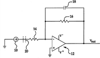
Fig. 1 is the synoptic diagram of transimpedance amplifier according to an embodiment of the invention;
Fig. 2 is the synoptic diagram of transimpedance amplifier according to another embodiment of the present invention;
Fig. 3 is the synoptic diagram according to the transimpedance amplifier of further embodiment of this invention;
Fig. 4 is the synoptic diagram according to the transimpedance amplifier of Fig. 3 of the programmable-gain of each grade of graphic extension; Can use described embodiment of the present invention; And
Fig. 5 is the planimetric map of spendable electronic component handler according to an embodiment of the invention;
Fig. 6 is the synoptic diagram of quick restoring current absorber of incorporating the transimpedance amplifier of with good grounds Fig. 1 into.
Embodiment
When testing capacitor assembly (for example multilayer ceramic capacitor (MLCC)) leakage current, because uncharged capacitance component is delivered to sensing circuit with some charging currents, therefore have the big electric current of described sensing circuit tolerance, wherein the major part of institute's delivered current is absorbed in the charging diode.Ideally, in a single day capacitance component is filled just delivered current no longer of electricity.And in the reality, leakage current by and be the important tolerance of quality (insulation resistance specifically) to the accurate measurement of this electric current to described capacitance component.
Routinely, this class testing is to use the circuit that comprises one or more operational amplifiers (opamps) with corresponding gain to carry out.For operational amplifier, in given configuration, before reaching capacity, operational amplifier exists to be great limited restriction to its input signal.When operational amplifier be in saturated in the time, the output of described operational amplifier is fixed on its plus or minus supply voltage place and is reduced to till wherein said operational amplifier is in its working range and the point of correct output signal can be provided up to input signal.How soon operational amplifier can walk out saturated is by several factor decisions, including (but not limited to) its output current source of supply ability, configuration and loading.When circuit contained more than an operational amplifier, the input of first order operational amplifier caused the saturated overload of output that level also is in the saturation conditions.
When testing in data acquisition, and speed is under the important situation, and expectation recovers rapidly so that can obtain accurate data and/or so that can obtain next group data rapidly in preset time from overload condition.Therefore, the described herein embodiment of the invention initiatively evicts out of this type of overload with metering circuit.
Fig. 1 shows transimpedance amplifier according to an embodiment of the invention.Fig. 1 comprises the current source 10 that steady current Iin is provided.Under the situation of given required output valve, current source 10 can be implemented by any number circuit design in those skilled in the art's the ken.For instance, current source 10 can represent to supply the combination of the voltage source of variable voltage, described variable voltage is coupled to the programmable current source described in the U.S. Patent Publication case of conveying jointly at 2008/0290879A1 number, and the full content of described patent disclosure case is incorporated herein with way of reference.
In Fig. 1, show capacitance component to be tested with dotted line, hereinafter be called device under test (DUT) 20.As hereinafter additionally at length discussing, after a plurality of these type of devices are connected to current source 10 and comprise the metering circuit of transimpedance amplifier, it is tested according to the order of sequence.
The transfer function of current sense amplifier 12 is Vout=-Iin*Rf, and this means for given input current, and output voltage V out is the mathematical product of input current and resistance value Rf.Ohmic value Rf is based on the designing requirement selection.For instance, suppose measured leakage current for+/-value between the lmA, wherein full scale represent the Vout place+/-5 volts.Can use the Rf value of 5k Ω.Full scale is defined based on application by the deviser.Hereinafter discuss the programming of Rf value in more detail about Fig. 4.
Fig. 2 comprises the transimpedance amplifier that has as the current sense amplifier 12 of Fig. 1 of the first order, wherein is added with the noninverting gain stage that is the noninverting voltage amplifier 22 of being arranged as of operational amplifier form.When attempting monitoring low level signal, can need one or more additional gain levels, gain stage for example seen in fig. 2.Can increase the Rf value in first amplifier again.Yet the inventor finds that this solution may be problematic when the operational amplifier of current sense amplifier 12 reaches its gain or bandwidth limit.And, in some cases, keep the Rf ohmic value to help the noise gain of system than I.The extra amplifier that is provided by the noninverting voltage amplifier in the second level allows the application logic identical with being used for the previous described first order to determine scope and ull-scale value.
In Fig. 2, the output of the first order (voltage Vin) is provided to the noninverting input of voltage amplifier 22.From the feedback that outputs to its anti-phase input of voltage amplifier 22 is to provide by the resistor 24 with R3 resistance value, and resistor 26 ground connection of anti-phase input by having the R2 resistance value.The transfer function of this gain stage is Vout=Vin* (1+R3/R2). as discussed previously, and be output as in the first order under the situation of Vin, the transfer function of the first order is Vin=-Iin*Rf.Therefore, under the situation of current known Iin and required maximum input voltage Vin and required maximum output voltage Vout, the appropriate value that can specify Rf, R3 and R2.For instance, belong at expection leakage current to be measured+/-l μ A (replace in the example as mentioned+/-1mA) between and full scale represent+/-situation of 5V under, the ohmic value of Rf equals 1.25M Ω, wherein partial gain (1+R3/R2) equals 4.
Although the second level is shown as noninverting voltage amplifier 22, operational amplifier alternately is arranged as hereinafter about the extra noninverting unity gain buffer of describing in detail of Fig. 4.Equally, based on teaching content herein, can comprise more than an amplifier stage if need.
Fig. 3 comprises first and second grade shown in Fig. 2 and adds from the partial additional feedback circuit that outputs to the anti-phase input of the first order.As shown in Figure 3, the output of the voltage amplifier 22 of the second noninverting gain stage is connected to two back-to-back Zener diodes 28.Zener diode 28 is connected in series to ground connection by resistor 30.The operational amplifier that is arranged as non-inverting buffer 32 is in Zener diode 28 back.That is, Zener diode 28 is coupled between the noninverting input of impact damper 32 and the output and its anti-phase input that feedback path 34 is provided in impact damper 32.The output of impact damper 32 is connected to back-to-back signal diode 36, and it is coupled to the anti-phase input of the current sense amplifier 12 of the first order again.More particularly, Fig. 1 and 2 resistor 14 are substituted by resistor 14a among Fig. 3 and 14b, and are connected to node 38 between resistor 14a and the 14b by the feedback circuit that back-to-back Zener diode 28, non-inverting buffer 32 and back-to-back signal diode 36 provide.
In this circuit, the input current in expectation, desired extent allows the transfer function determine of the described as discussed previously level of described circuit to turn round with linear mode.During normal running, back-to-back Zener diode 28 prevents that electric current from flowing to feedback path, because Vout is lower than the forward voltage of Zener diode.Non-inverting buffer 32 is inertias, and back-to-back signal diode 36 prevents that electric current from flowing to the output of non-inverting buffer 32 from node 38.Yet, to the input current of described circuit (that is, input current to the anti-phase input of first order current sense amplifier 12) goes beyond the scope and enough greatly with the outputing under any one the situation in its rail of driving amplifier, begin to move towards its power rail from the voltage output Vout of voltage amplifier 22.In case enough greatly with conducting Zener diode 28, then Vout will be in the clamping voltage place of Zener diode 28.Then, clamping voltage is provided to non-inverting buffer 32, it is to select by expectation at high current driving ability.Electric current from the output of impact damper 32 is fed to signal diode, and described signal diode begins conduction after the enough electric currents from impact damper 32 are fed to it, this again the current potential at active drive node 38 places reduce.Along with this current potential reduces, the input signal that current sense amplifier 12 is experienced reduces to allow described amplifier to begin to recover from the overload of its input.
Although Fig. 3 graphic extension is from the partial feedback circuit that outputs to the anti-phase input of the first order, the feedback circuit of Fig. 3 can be implemented by the single level of institute's teaching among Fig. 1.At least for stability reasons, this does not normally more expect, but possible.Equally, the configuration of Fig. 3 can be by using as coming the non-inverting amplifier 22 of alternate figures 2 to implement about the described impact damper of Fig. 4.
As shown in Figure 4, the gain in the circuit topology can be programmable.In Fig. 4, both gains of the first order and the second level can depend upon and should be used for programming.Except being configured to shown in Fig. 3, Fig. 4 also comprises the field programmable gate array (FPGA) 50 that is coupled at two feedback circuits of current sense amplifier 12.More particularly, first feedback circuit 52 comprises resistor 16a and the capacitor 18a that is arranged in parallel, and second feedback circuit 54 comprises resistor 16b and the capacitor 18b that is arranged in parallel.About as described in the resistor 16, the value of 16a or 16b was Rf as before.More than two feedback circuits also is possible.FPGA 50 inserts to switch through programming, that is, depend upon control signal 1 and 2 and enable first or second feedback circuit 52,54.Similarly, the switch 56 for the resistor 26 that is coupled to noninverting voltage amplifier 22 provides optional control.By control signal 3 being applied to switch 56, resistor 26 (having value R2) changeable place in circuit and dialysis circuit.To recognize that omitting resistor 26 will be noninverting unity gain buffer from the configuration change of noninverting voltage amplifier 22 to the configuration of operational amplifier according to this explanation as the those skilled in the art.When output signal Vin did not need to amplify, this configuration was useful.As in the argumentation of Fig. 3, can omit the second level on the whole if desired.
Control signal 1,2 and 3 is in this embodiment provided by microcomputer, except various inputs and output connection, described microcomputer also comprises random-access memory (ram), ROM (read-only memory) (ROM), keeps activating storer (KAM), CPU (central processing unit) (CPU) etc.For instance, hereinafter about in the described application of Fig. 5, described microcomputer runs software program comprises by the user and presents setup menu to carry out described test, and it comprises information such as the expection leakage current of the size that for example depends upon capacitance component and corresponding full scale voltage.As the response to this menu, microcomputer can be by the control signal 1,2 and 3 that is provided to FPGA 50 and switch 56 gain of programming.Certainly, the function of FPGA 50 can be implemented by one or more nextport hardware component NextPorts.Can use any number solid-state switch to implement switch 56.
In circuit topology, have any instrument that programmable-gain allows to contain described circuit and have big dynamic range.For instance, measurement capability can between+/-scope of leakage current values between the 1mA in, its intermediate-resolution down to+/-200pA.When this type of is accurately measured when needs, only use the fixed value of Rf, R3 and R2 to be difficult to realize this task.Become a plurality of districts to make described task for related hardware, be easier to this range subdivision.In these scopes, the ohmic value of Rf, R3 and R2 can be specified by full scale voltage and the partial yield value that defines each scope as indicated above.When the big dynamic range of appliance requires, can be by the ohmic value of the Rf of expectation program current sensing amplifier 12 and the gain of amplifier 22.Then, do not depend upon scope, if to the input current of described circuit enough greatly to cause overload, then towards the output of Zener diode 28 forward voltage driving amplifiers 22 at current sense amplifier 12 places.In case reach described voltage, then feedback network activates, thereby in case the product that auxiliary described circuit turns back to the gain of the output voltage of its range of linearity and current sense amplifier 12 and amplifier 22 than amplifier 12 or 22 by self attainable speed fasterly be lower than the Zener diode forward voltage then turn-off.Described circuit is got back in its range of linearity.
As mentioned, when expection leakage current values scope, it is desired segmenting described scope and controlling programmable-gain based on each scope.Following table provides the value of four different range of leakage current as the example of the application of programmable-gain teaching of the present invention.
| The leakage current scope (+/-) | Value Rf (K Ω) | Partial gain |
| 3μA | 324 | 4 |
| 12μA | 324 | 1 |
| |
20 | 4 |
| |
20 | 1 |
These scopes can be in the embodiment of Fig. 4 be associated with resistor 16a by the value Rf with 324K Ω and the value Rf of 20K Ω are associated with resistor 16b and implement.Then, these values can optionally be switched by PFGA 50. Resistor 24 and 26 resistance value will be through setting so that gain is 4, and for instance, value R3 can be 3K Ω, and the value of R2 can be 1K Ω.Then, the gain of amplifier 22 can optionally be switched to depend upon required scope by switch 56 and change gain between 1 and 4.
Can be embodied as the part of any number independent test device of using that is used for the testing capacitor assembly according to any one the circuit among Fig. 1 to 4.In the device that transimpedance amplifier also may be implemented in current source separates.Then, current source can be any programmable calculator Controlling Source, for example can from the Electro Scient Ind Inc of Portland (Portland) (Electro Scientific Industries, Inc.) or the assignee of the present application for patent 54XX power supply model of buying.It is in the electronic component handler of a large amount of electronic packages of test in the short relatively time cycle that a certain desired of transimpedance amplifier is used.These disposers are including (but not limited to) (the Electro Scientific Industries of Electro Scient Ind Inc, Inc.) product sold, various electronic component handlers are sold by described company, including (but not limited to) the high capacity MLCC test machine of selling as model 3500.
Electronic component handler device be illustrated in name be called " circuit unit disposer (Electrical Circuit Component Handler) " the 5th, 842, No. 579 common transference United States Patent (USP)s, the full content of described patent is incorporated herein with way of reference.The whole diagrammatic sketch of Fig. 5 display circuit component handling device 100.Disposer 100 has and defines the loading frame 112 that loads zone 130, defines a plurality of test modules 114 of test zone 115 and define the part 160 that blows off in the zone 170 of blowing off.In operation, electronic package is delivered to load in the zone 130 by loading frame 112 and goes up in the test bench 124 that exists with the auxiliary test board (its integral body does not show) that individually is drawn onto by vacuum.Be in the test zone 115 after the test suite that described assembly moves to the zone 170 of blowing off, the part 160 that wherein blows off removes vacuum and comes classification element based on test result.
Although do not show in detail,, then it can be electrically coupled to test module 114 for use in testing for each assembly in the test zone 115 if the embodiment of the invention and current source 10 are implemented separately.That is to say that the assembly on the test bench 124 stands a plurality of tests by use test module 114 in test zone 115.For instance, when test MLCC, provide data usually about (for example) electric capacity, dissipation factor and insulation resistance.Then, can use the data that obtain from test to come and find out defective those parts by the tolerance limit classification element.
Briefly explaination as mentioned in operation, when uncharged capacitor enters test, herein for being placed on the test bench 124, requires to carry out according to the order of sequence to test according to individual manufacturer thereby charging current and charging voltage are put on this DUT 20.About insulation resistance (IR) test, charging current is put on DUT 20 from current source 10 produce big electric current, thereby produce overload in the transimpedance amplifier that the overload with current sense amplifier 10 begins.Along with the charging to DUT 20, the electric current that experiences in the anti-phase input of current sense amplifier 12 begins to descend.After one period short time, to the leakage current that is input as of current sense amplifier 12.Measured leakage current is represented the insulation resistance of DUT 20.By select the release time of minimum current sensing amplifier 12 and (if being fit to) voltage amplifier 22 at the suitable gain of the feedback circuit of each grade and Fig. 3 (when using).When DUT 20 was big value capacitor (wherein leakage current is high relatively), be even more important little release time.If (that is, before overload finishes) measures before recovering to finish, then measure the response that to catch the metering circuit recovery but not actual leakage current.In high speed test, this more is a risk.
The problem of the initial release time of transshipping and being produced also can be complicated because of other test that may carry out before insulation resistance (IR) test.This class testing is the contact checkout.The contact checkout is used to check parts to be tested (for example DUT 20) whether suitably to arrive test board.According to a known embodiment, produce 1 volt of peak to peak high-frequency sine wave by DUT20, and measure gained AC electric current and exist the predetermined threshold value of DUT 20 to compare with indication it.Carry out this measurement with the sensing circuit that trans-impedance amplifier according to the present invention separates from shared entrance.This applies charging voltage can cause any one the circuit among Fig. 1 to 3 to transship.Depend upon and carry out the soak time that the IR measurement is allowed before, may need the fast quick-recovery of current sense amplifier 12 and voltage amplifier 22 because this early tests.
The inventive concepts of institute's teaching can be incorporated in the 2008/0290879A1 U.S. Patent Publication case has teaching content of the present invention to obtain additional benefit.Fig. 6 graphic extension is randomly added quick restoring current absorber 46 according to the teaching content of 2008/0290879A1 U.S. Patent Publication case to the metering circuit of Fig. 1.
In Fig. 6, restoring current absorber 46 is connected tap 60 places and the ground connection between DUT 20 and the resistor 14 fast.Clamping diode circuit 40 is provided by two diodes 42,44, and described two diodes are arranged in parallel so that the anode of the negative electrode of the plus earth of the anode of first diode 42 and second diode 44 and first diode 42 and second diode 44 is electrically coupled to tap 60.Catching diode 42,44 charging currents for DUT 20 provide the electric current return path.In addition, catching diode 42,44 voltage by clamp current source 10 when DUT 20 short circuits comes to provide input protection for current sense amplifier 12.Notice that although for simplifying the demonstration in Fig. 1 to 4 of explanation to transimpedance amplifier, catching diode 42,44 can be incorporated among each embodiment of the present invention similarly.
The switch 70 that the leap clamping diode circuit 40 of 2008/0290879A1 U.S. Patent Publication case is connected in parallel is implemented by solid-state relay herein, only for instance, can be from El Segundo international rectifier (International Rectifier ofEl Segundo, the PVG612 power MOSFET photovoltaic relay of CA) buying in California.When DUT 20 is just charged by current source 10, control signal 48 Closing Switch 70 of coming self-controller.Then, before measuring leakage current, open switch 70 by transimpedance amplifier.
The teaching content of the application of the invention, eliminated that coordination switch described in the 2008/0290879A1 U.S. Patent Publication case is enabled and charging circuit of stopping using (comprising absorber 46) and metering circuit between the needs of timing.Before measuring leakage current, current sink 46 is switched to when opening the change that produces the current potential of current sense amplifier 12.Therefore, when using, exist the gained of output place of current sense amplifier 12 and voltage amplifier 22 to change.The overload recovery component of the transimpedance amplifier of institute's teaching is auxiliary herein reduces any voltage disturbance, thereby allows to carry out fast after switch current absorber 46 leakage current measurement.
When the high value of test capacitor, the combination of these teaching contents is useful especially.This is because when current sink 46 switches dialysis, changes immediately to the value of the input of current sense amplifier 12, and this is owing to due to the high impedance of whole transimpedance amplifier.This value depends upon the input impedance value Rin of transimpedance amplifier and the value Rf of current sense amplifier 12.The voltage gain of transimpedance amplifier is followed transfer function Vout=-Rf/Rin.If value Rf measures required greatly as receiving volt level amplifier (nano-amp) and skin volt level amplifier (pico-amp), then the initial overload to current sense amplifier 12 is possible.Because the overload of transimpedance amplifier is recovered, overload news speed disappears.
Although Fig. 6 shows the quick restoring current absorber 46 be coupled to Fig. 1 transimpedance amplifier, restoring current absorber 46 can be incorporated in the embodiment of the invention any one fast, comprises those embodiment shown about Fig. 2 to 4 and that describe.
Capacitance component leakage current measurement in the production environment not only needs accuracy but also need speed.Embodiment with transimpedance amplifier that overload recovers allows that any initial overload reduces rapidly in the front-end circuit, limits the delay that positive tested person capacitance component is full of the time of electricity that surpasses of leakage current measurement thus.And the described measurement that the embodiment of enforcement transimpedance amplifier reduces so to carry out will reflect its recovery but not the risk of actual leakage current.
Embodiment mentioned above has been described, so that allow easily to understand the present invention, and unrestricted the present invention.On the contrary, the present invention plans to contain various modifications and the equivalent arrangements that is comprised in the spirit of aforesaid right claim and the scope, and described scope is consistent with the explanation of broad sense, so that include all this type of modification and equivalent structures under the permission of law.
Claims (15)
1. equipment that is used to measure the leakage current of capacitance component, described equipment comprises at least one operational amplifier, and described equipment comprises:
First order amplifier, it is configured to receive input so that described capacitance component is coupled in series to current source in anti-phase input from the capacitance component that is connected in series, and will be supplied to the described anti-phase input of described first order amplifier from the electric current that described capacitance component flows through; And
The feedback path of described first order amplifier is coupled between the output and described anti-phase input of described first order amplifier, and comprise feedback resistor, the resistance value of described feedback resistor depends upon the desired value of described leakage current and the corresponding full scale voltage of described first order amplifier.
2. equipment according to claim 1, wherein said feedback path comprises at least two feedback circuits, and each feedback circuit comprises resistor, and described equipment further comprises:
Be used for by switching the programme member of described first order amplifier gain of described at least two feedback circuits.
3. according to claim 1 or the described equipment of claim 2, it further comprises:
Second level amplifier, it is coupled to the described output of described first order amplifier, and described second level amplifier comprises programmable-gain.
4. equipment according to claim 3, it further comprises:
Be used for described programmable-gain is switched to member greater than the value of unity gain from unity gain.
5. equipment according to claim 3, the noninverting input of described second level amplifier is coupled in the described output of wherein said first order amplifier.
6. equipment according to claim 5, wherein said second level amplifier comprises programmable-gain, and described equipment further comprises:
Switch, it is configured to described programmable-gain is switched to value greater than unity gain from unity gain.
7. equipment according to claim 6, it further comprises:
Feedback path, it is from the summing junction of the described anti-phase input that outputs to described first order amplifier of described second level amplifier.
8. equipment according to claim 7, wherein the described feedback path from the described summing junction of the described anti-phase input that exports described first order amplifier to of described second level amplifier comprises:
Be used to prevent flow the member up to the described output of described second level amplifier surpass the value of institute confining spectrum till of electric current from the described summing junction of the described anti-phase input that outputs to described first order amplifier of described second level amplifier; And
Be used to limit electric current at the mobile member of the direction of described output from described summing junction to described second level amplifier.
9. equipment according to claim 8, wherein said institute confining spectrum comprises the value greater than the saturation voltage of described second level amplifier.
10. equipment according to claim 7, wherein said feedback path comprises:
Back-to-back Zener diode, it is coupled to the described output of described second level amplifier;
The impact damper amplifier, it comprises the noninverting input of being coupled to described back-to-back Zener diode; And
Back-to-back signal diode, it is coupled to the output of described impact damper amplifier and is coupled to the described summing junction of the described anti-phase input of described first order amplifier.
11. equipment according to claim 1, it further comprises:
Second feedback path, it is from the described described anti-phase input that outputs to described first order amplifier of described first order amplifier, and described second feedback path is configured to reduce to go to the input of described anti-phase input when the output valve of described first order amplifier is indicated described first order amplifier saturated.
12. according to claim 1 or the described equipment of claim 2, it further comprises:
Second level amplifier, it is coupled to the described output of described first order amplifier; And
Second feedback path, it is from the described anti-phase input that outputs to described first order amplifier of described second level amplifier, and described second feedback path is configured to reduce to go to the input of described anti-phase input when the output valve of described second level amplifier is indicated described second level amplifier saturated.
13. equipment according to claim 1, it further comprises:
Programmable device, it is configured to depend upon the described corresponding full scale voltage of the described desired value of described leakage current and described first order amplifier and described feedback resistor is switched to second value from first value.
14. equipment according to claim 12, wherein said second feedback path comprises:
Clamping diode circuit, it is coupled to the described anti-phase input of described first order amplifier.
15. equipment according to claim 1, it further comprises:
Input resistance, it is coupled between the described anti-phase input of described capacitance component that is connected in series and described first order amplifier, and the noninverting input grounding of wherein said first order amplifier.
Applications Claiming Priority (3)
| Application Number | Priority Date | Filing Date | Title |
|---|---|---|---|
| US12/059,752 US8054085B2 (en) | 2008-03-31 | 2008-03-31 | Programmable gain trans-impedance amplifier overload recovery circuit |
| US12/059,752 | 2008-03-31 | ||
| PCT/US2009/037062 WO2009123845A1 (en) | 2008-03-31 | 2009-03-13 | Programmable gain trans-impedance amplifier overload recovery circuit |
Publications (2)
| Publication Number | Publication Date |
|---|---|
| CN101981459A CN101981459A (en) | 2011-02-23 |
| CN101981459B true CN101981459B (en) | 2013-07-24 |
Family
ID=41116135
Family Applications (1)
| Application Number | Title | Priority Date | Filing Date |
|---|---|---|---|
| CN2009801112124A Expired - Fee Related CN101981459B (en) | 2008-03-31 | 2009-03-13 | Programmable gain trans-impedance amplifier overload recovery circuit |
Country Status (6)
| Country | Link |
|---|---|
| US (2) | US8054085B2 (en) |
| JP (1) | JP5498478B2 (en) |
| KR (1) | KR20100131490A (en) |
| CN (1) | CN101981459B (en) |
| TW (1) | TWI439706B (en) |
| WO (1) | WO2009123845A1 (en) |
Families Citing this family (17)
| Publication number | Priority date | Publication date | Assignee | Title |
|---|---|---|---|---|
| US8040124B2 (en) * | 2009-02-18 | 2011-10-18 | Advanced Ion Beam Technology, Inc. | Method and apparatus for monitoring leakage current of a faraday cup |
| TWI510130B (en) | 2010-09-20 | 2015-11-21 | Novatek Microelectronics Corp | Short detection circuit, light-emitting diode chip, light-emitting diode device and short detection method |
| US9086439B2 (en) * | 2011-02-25 | 2015-07-21 | Maxim Integrated Products, Inc. | Circuits, devices and methods having pipelined capacitance sensing |
| US9083297B2 (en) * | 2012-05-10 | 2015-07-14 | That Corporation | Programmable-gain amplifier |
| CN103852614A (en) * | 2012-11-29 | 2014-06-11 | 山东电力集团公司济宁供电公司 | Circuit for detecting leakage current of busbar |
| US8841971B1 (en) | 2012-12-17 | 2014-09-23 | Google Inc. | Short circuit current protection in an amplifier |
| CN105378492B (en) * | 2013-03-15 | 2018-10-02 | 伊利昂科技有限公司 | The device and method of the electric property of measurement of species |
| CN104345201A (en) * | 2013-08-09 | 2015-02-11 | 华为技术有限公司 | Leakage current detection method and device |
| US9625517B2 (en) | 2013-08-09 | 2017-04-18 | Huawei Technologies Co., Ltd. | Leakage current detection method and apparatus for detecting leakage of current from a board-mounted component |
| JP6417137B2 (en) * | 2014-07-14 | 2018-10-31 | 株式会社ヒューモラボラトリー | Capacitor insulation resistance measuring device |
| WO2017069776A1 (en) | 2015-10-23 | 2017-04-27 | Hewlett Packard Enterprise Development | Noise-canceling transimpedance amplifier (tia) systems |
| US10291207B2 (en) | 2016-07-07 | 2019-05-14 | Analog Devices, Inc. | Wide range programmable resistor for discrete logarithmic control, and tuning circuit for variable gain active filter using same |
| US10466296B2 (en) * | 2017-01-09 | 2019-11-05 | Analog Devices Global | Devices and methods for smart sensor application |
| EP3896848B1 (en) * | 2017-03-16 | 2023-11-01 | Isotopx Ltd | An amplifier |
| US10972063B2 (en) | 2018-10-17 | 2021-04-06 | Analog Devices Global Unlimited Company | Amplifier systems for measuring a wide range of current |
| CN112294187B (en) * | 2019-07-31 | 2024-03-15 | 苏州市春菊电器有限公司 | Dust cup dust amount detection device and detection method of dust collector |
| CN116699463B (en) * | 2023-07-28 | 2024-02-06 | 珠海禅光科技有限公司 | MLCC capacitor leakage current measuring method, device, control device and medium |
Citations (2)
| Publication number | Priority date | Publication date | Assignee | Title |
|---|---|---|---|---|
| US4862070A (en) * | 1987-10-30 | 1989-08-29 | Teradyne, Inc. | Apparatus for testing input pin leakage current of a device under test |
| CN101680921A (en) * | 2007-05-24 | 2010-03-24 | Esi电子科技工业公司 | Capacitance measurement with quick restoring current loop |
Family Cites Families (24)
| Publication number | Priority date | Publication date | Assignee | Title |
|---|---|---|---|---|
| JPS58102173A (en) | 1981-12-14 | 1983-06-17 | Fujitsu Ltd | Leakage current measuring circuit for capacitor |
| JPH01172765A (en) | 1987-12-28 | 1989-07-07 | Advantest Corp | Apparatus for measuring leak current of capacitive substance |
| US4931721A (en) | 1988-12-22 | 1990-06-05 | E. I. Du Pont De Nemours And Company | Device for automatically ascertaining capacitance, dissipation factor and insulation resistance of a plurality of capacitors |
| US5003486A (en) | 1989-02-24 | 1991-03-26 | Nero Technologies Ltd. | Programmable safety electrical socket controller |
| JP2841345B2 (en) | 1990-03-05 | 1998-12-24 | マルコン電子株式会社 | DC voltage application test circuit for capacitors |
| EP0468424B1 (en) | 1990-07-24 | 1995-07-12 | i f m electronic gmbh | Electronic switching apparatus with presence indicator |
| US5402329A (en) | 1992-12-09 | 1995-03-28 | Ernest H. Wittenbreder, Jr. | Zero voltage switching pulse width modulated power converters |
| JPH0777548A (en) | 1993-09-08 | 1995-03-20 | Ckd Corp | Jig for capacitor characteristics inspection apparatus |
| JP3457412B2 (en) * | 1995-01-11 | 2003-10-20 | 株式会社シバソク | Ultra low noise programmable DC power supply |
| JPH09113545A (en) * | 1995-10-16 | 1997-05-02 | Murata Mfg Co Ltd | Electric current measuring device |
| US5677634A (en) | 1995-11-16 | 1997-10-14 | Electro Scientific Industries, Inc. | Apparatus for stress testing capacitive components |
| US5842579A (en) | 1995-11-16 | 1998-12-01 | Electro Scientific Industries, Inc. | Electrical circuit component handler |
| JP3673589B2 (en) | 1996-03-05 | 2005-07-20 | ローム株式会社 | Method and apparatus for measuring capacitor leakage current |
| JP3663251B2 (en) | 1996-03-07 | 2005-06-22 | ローム株式会社 | Capacitor leakage current measurement method |
| JP3233037B2 (en) | 1996-08-26 | 2001-11-26 | 株式会社村田製作所 | Insulation resistance measuring device |
| US6011403A (en) * | 1997-10-31 | 2000-01-04 | Credence Systems Corporation | Circuit arrangement for measuring leakage current utilizing a differential integrating capacitor |
| US6008630A (en) | 1998-07-02 | 1999-12-28 | Compact Computer Corporation | Soft-switched built-in active snubber circuit |
| DE19842470A1 (en) | 1998-09-16 | 2000-03-23 | Siemens Ag | Earth-leakage circuit-breaker (elcb) arrangement with overload protection e.g. for electrical plant and equipment |
| MY121524A (en) * | 1999-09-22 | 2006-01-28 | Murata Manufacturing Co | Insulation resistance measuring apparatus for capacitive electronic parts |
| JP2002311074A (en) | 2001-04-09 | 2002-10-23 | Matsushita Electric Ind Co Ltd | Leakage current measurement method for capacitor |
| US6897731B2 (en) | 2003-10-24 | 2005-05-24 | Texas Instruments Incorporated | Method and circuit for overload recovery of an amplifier |
| JP4310695B2 (en) | 2004-03-30 | 2009-08-12 | アイシン精機株式会社 | Capacitance change detection device |
| JP2007129533A (en) * | 2005-11-04 | 2007-05-24 | New Japan Radio Co Ltd | Transimpedance amplifier |
| WO2007089937A2 (en) | 2006-01-27 | 2007-08-09 | Rudolph Technologies, Inc. | High-speed capacitor leakage measurement systems and methods |
-
2008
- 2008-03-31 US US12/059,752 patent/US8054085B2/en not_active Expired - Fee Related
-
2009
- 2009-03-13 WO PCT/US2009/037062 patent/WO2009123845A1/en active Application Filing
- 2009-03-13 CN CN2009801112124A patent/CN101981459B/en not_active Expired - Fee Related
- 2009-03-13 KR KR1020107023169A patent/KR20100131490A/en not_active Application Discontinuation
- 2009-03-13 JP JP2011503017A patent/JP5498478B2/en not_active Expired - Fee Related
- 2009-03-30 TW TW098110508A patent/TWI439706B/en not_active IP Right Cessation
-
2011
- 2011-11-08 US US13/291,758 patent/US8686739B2/en not_active Expired - Fee Related
Patent Citations (2)
| Publication number | Priority date | Publication date | Assignee | Title |
|---|---|---|---|---|
| US4862070A (en) * | 1987-10-30 | 1989-08-29 | Teradyne, Inc. | Apparatus for testing input pin leakage current of a device under test |
| CN101680921A (en) * | 2007-05-24 | 2010-03-24 | Esi电子科技工业公司 | Capacitance measurement with quick restoring current loop |
Non-Patent Citations (4)
| Title |
|---|
| JP特开2007-129533A 2007.05.24 |
| 冒依群.单片机在漏电流测量中的应用.《中国计量学院学报》.1990,第65-71页. |
| 冯肇瑞等.泄漏电流.《职业安全卫生词典》.四川人民出版社,1990,第328-329页. * |
| 单片机在漏电流测量中的应用;冒依群;《中国计量学院学报》;19901231;第65-71页 * |
Also Published As
| Publication number | Publication date |
|---|---|
| TWI439706B (en) | 2014-06-01 |
| JP5498478B2 (en) | 2014-05-21 |
| WO2009123845A9 (en) | 2010-11-04 |
| CN101981459A (en) | 2011-02-23 |
| US8054085B2 (en) | 2011-11-08 |
| KR20100131490A (en) | 2010-12-15 |
| US8686739B2 (en) | 2014-04-01 |
| TW200949268A (en) | 2009-12-01 |
| US20120049857A1 (en) | 2012-03-01 |
| WO2009123845A1 (en) | 2009-10-08 |
| US20090243636A1 (en) | 2009-10-01 |
| JP2011516859A (en) | 2011-05-26 |
Similar Documents
| Publication | Publication Date | Title |
|---|---|---|
| CN101981459B (en) | Programmable gain trans-impedance amplifier overload recovery circuit | |
| US10782334B2 (en) | Testing MOS power switches | |
| CN101949990B (en) | IC pin open short circuit test method | |
| JP6390359B2 (en) | Inspection method and inspection apparatus for photovoltaic power generation system | |
| JP2016213955A (en) | Solar cell inspection apparatus and solar cell inspection method | |
| CN106341032A (en) | Electric power conversion device | |
| CN107534314A (en) | Current limit | |
| CN107991542B (en) | A kind of active antenna detection device and its detection method | |
| US10317248B2 (en) | Multiple-distance proximity sensor systems | |
| US20150380774A1 (en) | Battery state monitoring circuit and battery device | |
| US10944259B2 (en) | System and method for over voltage protection in both positive and negative polarities | |
| US6859058B2 (en) | Method and apparatus for testing electronic devices | |
| CN105974202A (en) | Micro-capacitance reference measurement circuit with multiple measuring ranges and measurement method thereof | |
| US11499995B2 (en) | Leakage compensation technique for current sensor | |
| US9121876B2 (en) | Generated power output measuring apparatus | |
| CN104614643A (en) | Device and method for detecting short circuit location in line | |
| CN214750559U (en) | Loop impedance detection device | |
| JP6189199B2 (en) | Contact inspection apparatus, contact inspection method, and electronic component | |
| CN211263623U (en) | Loop resistance tester | |
| CN210899115U (en) | Diode test unit and device | |
| Kostka et al. | Practical Implementation of a Concept for In-Situ Detection of Humidity-Related Degradation of IGBT Modules | |
| KR20160008470A (en) | Device for measuring insulation resistance of capacitor | |
| CN112611974A (en) | Storage battery internal resistance detection device | |
| JPH1164410A (en) | Program power device with decoupling capacity-measurement function | |
| CN115667949A (en) | Switching device for a direct current network and operating method for a switching device |
Legal Events
| Date | Code | Title | Description |
|---|---|---|---|
| C06 | Publication | ||
| PB01 | Publication | ||
| C10 | Entry into substantive examination | ||
| SE01 | Entry into force of request for substantive examination | ||
| C14 | Grant of patent or utility model | ||
| GR01 | Patent grant | ||
| CF01 | Termination of patent right due to non-payment of annual fee |
Granted publication date: 20130724 Termination date: 20160313 |
|
| CF01 | Termination of patent right due to non-payment of annual fee |