KR101452949B1 - Semiconductor device and method of manufacturing the same - Google Patents
Semiconductor device and method of manufacturing the same Download PDFInfo
- Publication number
- KR101452949B1 KR101452949B1 KR1020097014375A KR20097014375A KR101452949B1 KR 101452949 B1 KR101452949 B1 KR 101452949B1 KR 1020097014375 A KR1020097014375 A KR 1020097014375A KR 20097014375 A KR20097014375 A KR 20097014375A KR 101452949 B1 KR101452949 B1 KR 101452949B1
- Authority
- KR
- South Korea
- Prior art keywords
- delete delete
- trench
- layer
- charge
- trenches
- Prior art date
Links
- 239000004065 semiconductor Substances 0.000 title claims abstract description 200
- 238000004519 manufacturing process Methods 0.000 title description 58
- 239000003989 dielectric material Substances 0.000 claims abstract description 147
- 238000000034 method Methods 0.000 claims description 171
- 239000000463 material Substances 0.000 claims description 50
- VYPSYNLAJGMNEJ-UHFFFAOYSA-N Silicium dioxide Chemical compound O=[Si]=O VYPSYNLAJGMNEJ-UHFFFAOYSA-N 0.000 claims description 24
- 229910052814 silicon oxide Inorganic materials 0.000 claims description 14
- 229910052782 aluminium Inorganic materials 0.000 claims description 11
- XAGFODPZIPBFFR-UHFFFAOYSA-N aluminium Chemical compound [Al] XAGFODPZIPBFFR-UHFFFAOYSA-N 0.000 claims description 11
- 229910052792 caesium Inorganic materials 0.000 claims description 11
- WKBOTKDWSSQWDR-UHFFFAOYSA-N Bromine atom Chemical compound [Br] WKBOTKDWSSQWDR-UHFFFAOYSA-N 0.000 claims description 10
- GDTBXPJZTBHREO-UHFFFAOYSA-N bromine Substances BrBr GDTBXPJZTBHREO-UHFFFAOYSA-N 0.000 claims description 10
- 229910052794 bromium Inorganic materials 0.000 claims description 10
- VYZAMTAEIAYCRO-UHFFFAOYSA-N Chromium Chemical compound [Cr] VYZAMTAEIAYCRO-UHFFFAOYSA-N 0.000 claims description 9
- 229910052804 chromium Inorganic materials 0.000 claims description 9
- 239000011651 chromium Substances 0.000 claims description 9
- PNDPGZBMCMUPRI-UHFFFAOYSA-N iodine Chemical compound II PNDPGZBMCMUPRI-UHFFFAOYSA-N 0.000 claims description 9
- VEXZGXHMUGYJMC-UHFFFAOYSA-M Chloride anion Chemical compound [Cl-] VEXZGXHMUGYJMC-UHFFFAOYSA-M 0.000 claims description 3
- -1 cesium ions Chemical class 0.000 claims description 3
- 239000012535 impurity Substances 0.000 abstract description 9
- 239000010410 layer Substances 0.000 description 539
- 230000008569 process Effects 0.000 description 115
- 239000000758 substrate Substances 0.000 description 81
- 238000012986 modification Methods 0.000 description 35
- 230000004048 modification Effects 0.000 description 35
- 230000015556 catabolic process Effects 0.000 description 31
- 229910021420 polycrystalline silicon Inorganic materials 0.000 description 26
- 229920005591 polysilicon Polymers 0.000 description 26
- 150000001875 compounds Chemical class 0.000 description 24
- 239000007943 implant Substances 0.000 description 21
- 229910052710 silicon Inorganic materials 0.000 description 21
- 239000010703 silicon Substances 0.000 description 21
- 238000002513 implantation Methods 0.000 description 20
- 230000000873 masking effect Effects 0.000 description 20
- 229910052581 Si3N4 Inorganic materials 0.000 description 19
- HQVNEWCFYHHQES-UHFFFAOYSA-N silicon nitride Chemical compound N12[Si]34N5[Si]62N3[Si]51N64 HQVNEWCFYHHQES-UHFFFAOYSA-N 0.000 description 19
- 239000011800 void material Substances 0.000 description 19
- 150000002500 ions Chemical class 0.000 description 18
- XUIMIQQOPSSXEZ-UHFFFAOYSA-N Silicon Chemical compound [Si] XUIMIQQOPSSXEZ-UHFFFAOYSA-N 0.000 description 17
- 238000000137 annealing Methods 0.000 description 17
- 239000010409 thin film Substances 0.000 description 17
- 238000010586 diagram Methods 0.000 description 16
- 238000005530 etching Methods 0.000 description 16
- 238000009792 diffusion process Methods 0.000 description 15
- 229910052751 metal Inorganic materials 0.000 description 14
- 239000004020 conductor Substances 0.000 description 13
- 239000002184 metal Substances 0.000 description 13
- 238000005137 deposition process Methods 0.000 description 12
- 238000013461 design Methods 0.000 description 12
- 229910052787 antimony Inorganic materials 0.000 description 11
- WATWJIUSRGPENY-UHFFFAOYSA-N antimony atom Chemical compound [Sb] WATWJIUSRGPENY-UHFFFAOYSA-N 0.000 description 11
- 229910052785 arsenic Inorganic materials 0.000 description 11
- RQNWIZPPADIBDY-UHFFFAOYSA-N arsenic atom Chemical compound [As] RQNWIZPPADIBDY-UHFFFAOYSA-N 0.000 description 11
- 230000015572 biosynthetic process Effects 0.000 description 11
- 239000002019 doping agent Substances 0.000 description 10
- BHEPBYXIRTUNPN-UHFFFAOYSA-N hydridophosphorus(.) (triplet) Chemical compound [PH] BHEPBYXIRTUNPN-UHFFFAOYSA-N 0.000 description 10
- ZOXJGFHDIHLPTG-UHFFFAOYSA-N Boron Chemical compound [B] ZOXJGFHDIHLPTG-UHFFFAOYSA-N 0.000 description 9
- 230000008901 benefit Effects 0.000 description 9
- 229910052796 boron Inorganic materials 0.000 description 9
- 238000001465 metallisation Methods 0.000 description 9
- TVFDJXOCXUVLDH-UHFFFAOYSA-N caesium atom Chemical compound [Cs] TVFDJXOCXUVLDH-UHFFFAOYSA-N 0.000 description 8
- 229920002120 photoresistant polymer Polymers 0.000 description 8
- IRPGOXJVTQTAAN-UHFFFAOYSA-N 2,2,3,3,3-pentafluoropropanal Chemical compound FC(F)(F)C(F)(F)C=O IRPGOXJVTQTAAN-UHFFFAOYSA-N 0.000 description 7
- KLZUFWVZNOTSEM-UHFFFAOYSA-K Aluminum fluoride Inorganic materials F[Al](F)F KLZUFWVZNOTSEM-UHFFFAOYSA-K 0.000 description 7
- 239000006227 byproduct Substances 0.000 description 7
- 230000005684 electric field Effects 0.000 description 7
- 239000000945 filler Substances 0.000 description 7
- 239000012212 insulator Substances 0.000 description 7
- 238000005468 ion implantation Methods 0.000 description 7
- ZAMOUSCENKQFHK-UHFFFAOYSA-N Chlorine atom Chemical compound [Cl] ZAMOUSCENKQFHK-UHFFFAOYSA-N 0.000 description 6
- 239000000460 chlorine Substances 0.000 description 6
- 229910052801 chlorine Inorganic materials 0.000 description 6
- BOTDANWDWHJENH-UHFFFAOYSA-N Tetraethyl orthosilicate Chemical compound CCO[Si](OCC)(OCC)OCC BOTDANWDWHJENH-UHFFFAOYSA-N 0.000 description 5
- 235000012239 silicon dioxide Nutrition 0.000 description 5
- 239000000377 silicon dioxide Substances 0.000 description 5
- ZLMJMSJWJFRBEC-UHFFFAOYSA-N Potassium Chemical compound [K] ZLMJMSJWJFRBEC-UHFFFAOYSA-N 0.000 description 4
- 229910004298 SiO 2 Inorganic materials 0.000 description 4
- 230000001413 cellular effect Effects 0.000 description 4
- 230000000694 effects Effects 0.000 description 4
- 239000011295 pitch Substances 0.000 description 4
- 229910052700 potassium Inorganic materials 0.000 description 4
- 239000011591 potassium Substances 0.000 description 4
- 229910016569 AlF 3 Inorganic materials 0.000 description 3
- OAICVXFJPJFONN-UHFFFAOYSA-N Phosphorus Chemical compound [P] OAICVXFJPJFONN-UHFFFAOYSA-N 0.000 description 3
- 150000004767 nitrides Chemical class 0.000 description 3
- 229910052698 phosphorus Inorganic materials 0.000 description 3
- 239000011574 phosphorus Substances 0.000 description 3
- 238000001020 plasma etching Methods 0.000 description 3
- 239000011241 protective layer Substances 0.000 description 3
- 238000004088 simulation Methods 0.000 description 3
- IJGRMHOSHXDMSA-UHFFFAOYSA-N Atomic nitrogen Chemical compound N#N IJGRMHOSHXDMSA-UHFFFAOYSA-N 0.000 description 2
- 239000003990 capacitor Substances 0.000 description 2
- 238000007796 conventional method Methods 0.000 description 2
- 238000000151 deposition Methods 0.000 description 2
- 230000008021 deposition Effects 0.000 description 2
- 239000011810 insulating material Substances 0.000 description 2
- 238000009413 insulation Methods 0.000 description 2
- 238000013508 migration Methods 0.000 description 2
- 230000005012 migration Effects 0.000 description 2
- 239000000203 mixture Substances 0.000 description 2
- 238000007747 plating Methods 0.000 description 2
- 238000012545 processing Methods 0.000 description 2
- 230000009467 reduction Effects 0.000 description 2
- 239000007858 starting material Substances 0.000 description 2
- 239000002344 surface layer Substances 0.000 description 2
- 229910018072 Al 2 O 3 Inorganic materials 0.000 description 1
- 238000013459 approach Methods 0.000 description 1
- 230000000903 blocking effect Effects 0.000 description 1
- 210000000746 body region Anatomy 0.000 description 1
- 238000004364 calculation method Methods 0.000 description 1
- 230000008859 change Effects 0.000 description 1
- 239000002131 composite material Substances 0.000 description 1
- 238000005520 cutting process Methods 0.000 description 1
- 238000009826 distribution Methods 0.000 description 1
- 239000010408 film Substances 0.000 description 1
- 239000011521 glass Substances 0.000 description 1
- 238000002955 isolation Methods 0.000 description 1
- 239000007769 metal material Substances 0.000 description 1
- 229910052757 nitrogen Inorganic materials 0.000 description 1
- TWNQGVIAIRXVLR-UHFFFAOYSA-N oxo(oxoalumanyloxy)alumane Chemical compound O=[Al]O[Al]=O TWNQGVIAIRXVLR-UHFFFAOYSA-N 0.000 description 1
- 238000000059 patterning Methods 0.000 description 1
- 238000011112 process operation Methods 0.000 description 1
- 239000000047 product Substances 0.000 description 1
- 238000004080 punching Methods 0.000 description 1
- 210000001747 pupil Anatomy 0.000 description 1
- 238000011084 recovery Methods 0.000 description 1
- 238000000926 separation method Methods 0.000 description 1
- 239000002356 single layer Substances 0.000 description 1
- 230000002277 temperature effect Effects 0.000 description 1
- WFKWXMTUELFFGS-UHFFFAOYSA-N tungsten Chemical compound [W] WFKWXMTUELFFGS-UHFFFAOYSA-N 0.000 description 1
- 229910052721 tungsten Inorganic materials 0.000 description 1
- 239000010937 tungsten Substances 0.000 description 1
- 235000012431 wafers Nutrition 0.000 description 1
Images


Classifications
-
- H—ELECTRICITY
- H01—ELECTRIC ELEMENTS
- H01L—SEMICONDUCTOR DEVICES NOT COVERED BY CLASS H10
- H01L29/00—Semiconductor devices adapted for rectifying, amplifying, oscillating or switching, or capacitors or resistors with at least one potential-jump barrier or surface barrier, e.g. PN junction depletion layer or carrier concentration layer; Details of semiconductor bodies or of electrodes thereof ; Multistep manufacturing processes therefor
- H01L29/66—Types of semiconductor device ; Multistep manufacturing processes therefor
- H01L29/68—Types of semiconductor device ; Multistep manufacturing processes therefor controllable by only the electric current supplied, or only the electric potential applied, to an electrode which does not carry the current to be rectified, amplified or switched
- H01L29/76—Unipolar devices, e.g. field effect transistors
- H01L29/772—Field effect transistors
- H01L29/78—Field effect transistors with field effect produced by an insulated gate
- H01L29/7801—DMOS transistors, i.e. MISFETs with a channel accommodating body or base region adjoining a drain drift region
- H01L29/7802—Vertical DMOS transistors, i.e. VDMOS transistors
-
- H—ELECTRICITY
- H01—ELECTRIC ELEMENTS
- H01L—SEMICONDUCTOR DEVICES NOT COVERED BY CLASS H10
- H01L21/00—Processes or apparatus adapted for the manufacture or treatment of semiconductor or solid state devices or of parts thereof
- H01L21/02—Manufacture or treatment of semiconductor devices or of parts thereof
- H01L21/02104—Forming layers
- H01L21/02107—Forming insulating materials on a substrate
- H01L21/02109—Forming insulating materials on a substrate characterised by the type of layer, e.g. type of material, porous/non-porous, pre-cursors, mixtures or laminates
- H01L21/02112—Forming insulating materials on a substrate characterised by the type of layer, e.g. type of material, porous/non-porous, pre-cursors, mixtures or laminates characterised by the material of the layer
- H01L21/02123—Forming insulating materials on a substrate characterised by the type of layer, e.g. type of material, porous/non-porous, pre-cursors, mixtures or laminates characterised by the material of the layer the material containing silicon
- H01L21/02164—Forming insulating materials on a substrate characterised by the type of layer, e.g. type of material, porous/non-porous, pre-cursors, mixtures or laminates characterised by the material of the layer the material containing silicon the material being a silicon oxide, e.g. SiO2
-
- H—ELECTRICITY
- H01—ELECTRIC ELEMENTS
- H01L—SEMICONDUCTOR DEVICES NOT COVERED BY CLASS H10
- H01L21/00—Processes or apparatus adapted for the manufacture or treatment of semiconductor or solid state devices or of parts thereof
- H01L21/02—Manufacture or treatment of semiconductor devices or of parts thereof
- H01L21/02104—Forming layers
- H01L21/02107—Forming insulating materials on a substrate
- H01L21/02109—Forming insulating materials on a substrate characterised by the type of layer, e.g. type of material, porous/non-porous, pre-cursors, mixtures or laminates
- H01L21/02112—Forming insulating materials on a substrate characterised by the type of layer, e.g. type of material, porous/non-porous, pre-cursors, mixtures or laminates characterised by the material of the layer
- H01L21/02123—Forming insulating materials on a substrate characterised by the type of layer, e.g. type of material, porous/non-porous, pre-cursors, mixtures or laminates characterised by the material of the layer the material containing silicon
- H01L21/0217—Forming insulating materials on a substrate characterised by the type of layer, e.g. type of material, porous/non-porous, pre-cursors, mixtures or laminates characterised by the material of the layer the material containing silicon the material being a silicon nitride not containing oxygen, e.g. SixNy or SixByNz
-
- H—ELECTRICITY
- H01—ELECTRIC ELEMENTS
- H01L—SEMICONDUCTOR DEVICES NOT COVERED BY CLASS H10
- H01L21/00—Processes or apparatus adapted for the manufacture or treatment of semiconductor or solid state devices or of parts thereof
- H01L21/02—Manufacture or treatment of semiconductor devices or of parts thereof
- H01L21/02104—Forming layers
- H01L21/02107—Forming insulating materials on a substrate
- H01L21/02296—Forming insulating materials on a substrate characterised by the treatment performed before or after the formation of the layer
- H01L21/02318—Forming insulating materials on a substrate characterised by the treatment performed before or after the formation of the layer post-treatment
- H01L21/02321—Forming insulating materials on a substrate characterised by the treatment performed before or after the formation of the layer post-treatment introduction of substances into an already existing insulating layer
-
- H—ELECTRICITY
- H01—ELECTRIC ELEMENTS
- H01L—SEMICONDUCTOR DEVICES NOT COVERED BY CLASS H10
- H01L21/00—Processes or apparatus adapted for the manufacture or treatment of semiconductor or solid state devices or of parts thereof
- H01L21/02—Manufacture or treatment of semiconductor devices or of parts thereof
- H01L21/04—Manufacture or treatment of semiconductor devices or of parts thereof the devices having at least one potential-jump barrier or surface barrier, e.g. PN junction, depletion layer or carrier concentration layer
- H01L21/18—Manufacture or treatment of semiconductor devices or of parts thereof the devices having at least one potential-jump barrier or surface barrier, e.g. PN junction, depletion layer or carrier concentration layer the devices having semiconductor bodies comprising elements of Group IV of the Periodic System or AIIIBV compounds with or without impurities, e.g. doping materials
- H01L21/20—Deposition of semiconductor materials on a substrate, e.g. epitaxial growth solid phase epitaxy
- H01L21/2003—Deposition of semiconductor materials on a substrate, e.g. epitaxial growth solid phase epitaxy characterised by the substrate
-
- H—ELECTRICITY
- H01—ELECTRIC ELEMENTS
- H01L—SEMICONDUCTOR DEVICES NOT COVERED BY CLASS H10
- H01L21/00—Processes or apparatus adapted for the manufacture or treatment of semiconductor or solid state devices or of parts thereof
- H01L21/02—Manufacture or treatment of semiconductor devices or of parts thereof
- H01L21/04—Manufacture or treatment of semiconductor devices or of parts thereof the devices having at least one potential-jump barrier or surface barrier, e.g. PN junction, depletion layer or carrier concentration layer
- H01L21/18—Manufacture or treatment of semiconductor devices or of parts thereof the devices having at least one potential-jump barrier or surface barrier, e.g. PN junction, depletion layer or carrier concentration layer the devices having semiconductor bodies comprising elements of Group IV of the Periodic System or AIIIBV compounds with or without impurities, e.g. doping materials
- H01L21/26—Bombardment with radiation
- H01L21/263—Bombardment with radiation with high-energy radiation
- H01L21/265—Bombardment with radiation with high-energy radiation producing ion implantation
- H01L21/2658—Bombardment with radiation with high-energy radiation producing ion implantation of a molecular ion, e.g. decaborane
-
- H—ELECTRICITY
- H01—ELECTRIC ELEMENTS
- H01L—SEMICONDUCTOR DEVICES NOT COVERED BY CLASS H10
- H01L21/00—Processes or apparatus adapted for the manufacture or treatment of semiconductor or solid state devices or of parts thereof
- H01L21/02—Manufacture or treatment of semiconductor devices or of parts thereof
- H01L21/04—Manufacture or treatment of semiconductor devices or of parts thereof the devices having at least one potential-jump barrier or surface barrier, e.g. PN junction, depletion layer or carrier concentration layer
- H01L21/18—Manufacture or treatment of semiconductor devices or of parts thereof the devices having at least one potential-jump barrier or surface barrier, e.g. PN junction, depletion layer or carrier concentration layer the devices having semiconductor bodies comprising elements of Group IV of the Periodic System or AIIIBV compounds with or without impurities, e.g. doping materials
- H01L21/28—Manufacture of electrodes on semiconductor bodies using processes or apparatus not provided for in groups H01L21/20 - H01L21/268
- H01L21/28008—Making conductor-insulator-semiconductor electrodes
-
- H—ELECTRICITY
- H01—ELECTRIC ELEMENTS
- H01L—SEMICONDUCTOR DEVICES NOT COVERED BY CLASS H10
- H01L21/00—Processes or apparatus adapted for the manufacture or treatment of semiconductor or solid state devices or of parts thereof
- H01L21/02—Manufacture or treatment of semiconductor devices or of parts thereof
- H01L21/04—Manufacture or treatment of semiconductor devices or of parts thereof the devices having at least one potential-jump barrier or surface barrier, e.g. PN junction, depletion layer or carrier concentration layer
- H01L21/18—Manufacture or treatment of semiconductor devices or of parts thereof the devices having at least one potential-jump barrier or surface barrier, e.g. PN junction, depletion layer or carrier concentration layer the devices having semiconductor bodies comprising elements of Group IV of the Periodic System or AIIIBV compounds with or without impurities, e.g. doping materials
- H01L21/30—Treatment of semiconductor bodies using processes or apparatus not provided for in groups H01L21/20 - H01L21/26
- H01L21/302—Treatment of semiconductor bodies using processes or apparatus not provided for in groups H01L21/20 - H01L21/26 to change their surface-physical characteristics or shape, e.g. etching, polishing, cutting
- H01L21/306—Chemical or electrical treatment, e.g. electrolytic etching
- H01L21/30604—Chemical etching
-
- H—ELECTRICITY
- H01—ELECTRIC ELEMENTS
- H01L—SEMICONDUCTOR DEVICES NOT COVERED BY CLASS H10
- H01L21/00—Processes or apparatus adapted for the manufacture or treatment of semiconductor or solid state devices or of parts thereof
- H01L21/02—Manufacture or treatment of semiconductor devices or of parts thereof
- H01L21/04—Manufacture or treatment of semiconductor devices or of parts thereof the devices having at least one potential-jump barrier or surface barrier, e.g. PN junction, depletion layer or carrier concentration layer
- H01L21/18—Manufacture or treatment of semiconductor devices or of parts thereof the devices having at least one potential-jump barrier or surface barrier, e.g. PN junction, depletion layer or carrier concentration layer the devices having semiconductor bodies comprising elements of Group IV of the Periodic System or AIIIBV compounds with or without impurities, e.g. doping materials
- H01L21/30—Treatment of semiconductor bodies using processes or apparatus not provided for in groups H01L21/20 - H01L21/26
- H01L21/324—Thermal treatment for modifying the properties of semiconductor bodies, e.g. annealing, sintering
-
- H—ELECTRICITY
- H01—ELECTRIC ELEMENTS
- H01L—SEMICONDUCTOR DEVICES NOT COVERED BY CLASS H10
- H01L21/00—Processes or apparatus adapted for the manufacture or treatment of semiconductor or solid state devices or of parts thereof
- H01L21/70—Manufacture or treatment of devices consisting of a plurality of solid state components formed in or on a common substrate or of parts thereof; Manufacture of integrated circuit devices or of parts thereof
- H01L21/71—Manufacture of specific parts of devices defined in group H01L21/70
- H01L21/76—Making of isolation regions between components
- H01L21/762—Dielectric regions, e.g. EPIC dielectric isolation, LOCOS; Trench refilling techniques, SOI technology, use of channel stoppers
- H01L21/76224—Dielectric regions, e.g. EPIC dielectric isolation, LOCOS; Trench refilling techniques, SOI technology, use of channel stoppers using trench refilling with dielectric materials
-
- H—ELECTRICITY
- H01—ELECTRIC ELEMENTS
- H01L—SEMICONDUCTOR DEVICES NOT COVERED BY CLASS H10
- H01L29/00—Semiconductor devices adapted for rectifying, amplifying, oscillating or switching, or capacitors or resistors with at least one potential-jump barrier or surface barrier, e.g. PN junction depletion layer or carrier concentration layer; Details of semiconductor bodies or of electrodes thereof ; Multistep manufacturing processes therefor
- H01L29/02—Semiconductor bodies ; Multistep manufacturing processes therefor
- H01L29/06—Semiconductor bodies ; Multistep manufacturing processes therefor characterised by their shape; characterised by the shapes, relative sizes, or dispositions of the semiconductor regions ; characterised by the concentration or distribution of impurities within semiconductor regions
- H01L29/0603—Semiconductor bodies ; Multistep manufacturing processes therefor characterised by their shape; characterised by the shapes, relative sizes, or dispositions of the semiconductor regions ; characterised by the concentration or distribution of impurities within semiconductor regions characterised by particular constructional design considerations, e.g. for preventing surface leakage, for controlling electric field concentration or for internal isolations regions
- H01L29/0607—Semiconductor bodies ; Multistep manufacturing processes therefor characterised by their shape; characterised by the shapes, relative sizes, or dispositions of the semiconductor regions ; characterised by the concentration or distribution of impurities within semiconductor regions characterised by particular constructional design considerations, e.g. for preventing surface leakage, for controlling electric field concentration or for internal isolations regions for preventing surface leakage or controlling electric field concentration
- H01L29/0611—Semiconductor bodies ; Multistep manufacturing processes therefor characterised by their shape; characterised by the shapes, relative sizes, or dispositions of the semiconductor regions ; characterised by the concentration or distribution of impurities within semiconductor regions characterised by particular constructional design considerations, e.g. for preventing surface leakage, for controlling electric field concentration or for internal isolations regions for preventing surface leakage or controlling electric field concentration for increasing or controlling the breakdown voltage of reverse biased devices
- H01L29/0615—Semiconductor bodies ; Multistep manufacturing processes therefor characterised by their shape; characterised by the shapes, relative sizes, or dispositions of the semiconductor regions ; characterised by the concentration or distribution of impurities within semiconductor regions characterised by particular constructional design considerations, e.g. for preventing surface leakage, for controlling electric field concentration or for internal isolations regions for preventing surface leakage or controlling electric field concentration for increasing or controlling the breakdown voltage of reverse biased devices by the doping profile or the shape or the arrangement of the PN junction, or with supplementary regions, e.g. junction termination extension [JTE]
- H01L29/063—Reduced surface field [RESURF] pn-junction structures
- H01L29/0634—Multiple reduced surface field (multi-RESURF) structures, e.g. double RESURF, charge compensation, cool, superjunction (SJ), 3D-RESURF, composite buffer (CB) structures
-
- H—ELECTRICITY
- H01—ELECTRIC ELEMENTS
- H01L—SEMICONDUCTOR DEVICES NOT COVERED BY CLASS H10
- H01L29/00—Semiconductor devices adapted for rectifying, amplifying, oscillating or switching, or capacitors or resistors with at least one potential-jump barrier or surface barrier, e.g. PN junction depletion layer or carrier concentration layer; Details of semiconductor bodies or of electrodes thereof ; Multistep manufacturing processes therefor
- H01L29/02—Semiconductor bodies ; Multistep manufacturing processes therefor
- H01L29/06—Semiconductor bodies ; Multistep manufacturing processes therefor characterised by their shape; characterised by the shapes, relative sizes, or dispositions of the semiconductor regions ; characterised by the concentration or distribution of impurities within semiconductor regions
- H01L29/0603—Semiconductor bodies ; Multistep manufacturing processes therefor characterised by their shape; characterised by the shapes, relative sizes, or dispositions of the semiconductor regions ; characterised by the concentration or distribution of impurities within semiconductor regions characterised by particular constructional design considerations, e.g. for preventing surface leakage, for controlling electric field concentration or for internal isolations regions
- H01L29/0642—Isolation within the component, i.e. internal isolation
- H01L29/0649—Dielectric regions, e.g. SiO2 regions, air gaps
- H01L29/0653—Dielectric regions, e.g. SiO2 regions, air gaps adjoining the input or output region of a field-effect device, e.g. the source or drain region
-
- H—ELECTRICITY
- H01—ELECTRIC ELEMENTS
- H01L—SEMICONDUCTOR DEVICES NOT COVERED BY CLASS H10
- H01L29/00—Semiconductor devices adapted for rectifying, amplifying, oscillating or switching, or capacitors or resistors with at least one potential-jump barrier or surface barrier, e.g. PN junction depletion layer or carrier concentration layer; Details of semiconductor bodies or of electrodes thereof ; Multistep manufacturing processes therefor
- H01L29/40—Electrodes ; Multistep manufacturing processes therefor
- H01L29/408—Electrodes ; Multistep manufacturing processes therefor with an insulating layer with a particular dielectric or electrostatic property, e.g. with static charges or for controlling trapped charges or moving ions, or with a plate acting on the insulator potential or the insulator charges, e.g. for controlling charges effect or potential distribution in the insulating layer, or with a semi-insulating layer contacting directly the semiconductor surface
-
- H—ELECTRICITY
- H01—ELECTRIC ELEMENTS
- H01L—SEMICONDUCTOR DEVICES NOT COVERED BY CLASS H10
- H01L29/00—Semiconductor devices adapted for rectifying, amplifying, oscillating or switching, or capacitors or resistors with at least one potential-jump barrier or surface barrier, e.g. PN junction depletion layer or carrier concentration layer; Details of semiconductor bodies or of electrodes thereof ; Multistep manufacturing processes therefor
- H01L29/66—Types of semiconductor device ; Multistep manufacturing processes therefor
- H01L29/66007—Multistep manufacturing processes
- H01L29/66075—Multistep manufacturing processes of devices having semiconductor bodies comprising group 14 or group 13/15 materials
- H01L29/66227—Multistep manufacturing processes of devices having semiconductor bodies comprising group 14 or group 13/15 materials the devices being controllable only by the electric current supplied or the electric potential applied, to an electrode which does not carry the current to be rectified, amplified or switched, e.g. three-terminal devices
- H01L29/66409—Unipolar field-effect transistors
- H01L29/66477—Unipolar field-effect transistors with an insulated gate, i.e. MISFET
- H01L29/66537—Unipolar field-effect transistors with an insulated gate, i.e. MISFET using a self aligned punch through stopper or threshold implant under the gate region
-
- H—ELECTRICITY
- H01—ELECTRIC ELEMENTS
- H01L—SEMICONDUCTOR DEVICES NOT COVERED BY CLASS H10
- H01L29/00—Semiconductor devices adapted for rectifying, amplifying, oscillating or switching, or capacitors or resistors with at least one potential-jump barrier or surface barrier, e.g. PN junction depletion layer or carrier concentration layer; Details of semiconductor bodies or of electrodes thereof ; Multistep manufacturing processes therefor
- H01L29/66—Types of semiconductor device ; Multistep manufacturing processes therefor
- H01L29/66007—Multistep manufacturing processes
- H01L29/66075—Multistep manufacturing processes of devices having semiconductor bodies comprising group 14 or group 13/15 materials
- H01L29/66227—Multistep manufacturing processes of devices having semiconductor bodies comprising group 14 or group 13/15 materials the devices being controllable only by the electric current supplied or the electric potential applied, to an electrode which does not carry the current to be rectified, amplified or switched, e.g. three-terminal devices
- H01L29/66409—Unipolar field-effect transistors
- H01L29/66477—Unipolar field-effect transistors with an insulated gate, i.e. MISFET
- H01L29/66666—Vertical transistors
-
- H—ELECTRICITY
- H01—ELECTRIC ELEMENTS
- H01L—SEMICONDUCTOR DEVICES NOT COVERED BY CLASS H10
- H01L29/00—Semiconductor devices adapted for rectifying, amplifying, oscillating or switching, or capacitors or resistors with at least one potential-jump barrier or surface barrier, e.g. PN junction depletion layer or carrier concentration layer; Details of semiconductor bodies or of electrodes thereof ; Multistep manufacturing processes therefor
- H01L29/66—Types of semiconductor device ; Multistep manufacturing processes therefor
- H01L29/66007—Multistep manufacturing processes
- H01L29/66075—Multistep manufacturing processes of devices having semiconductor bodies comprising group 14 or group 13/15 materials
- H01L29/66227—Multistep manufacturing processes of devices having semiconductor bodies comprising group 14 or group 13/15 materials the devices being controllable only by the electric current supplied or the electric potential applied, to an electrode which does not carry the current to be rectified, amplified or switched, e.g. three-terminal devices
- H01L29/66409—Unipolar field-effect transistors
- H01L29/66477—Unipolar field-effect transistors with an insulated gate, i.e. MISFET
- H01L29/66674—DMOS transistors, i.e. MISFETs with a channel accommodating body or base region adjoining a drain drift region
- H01L29/66712—Vertical DMOS transistors, i.e. VDMOS transistors
- H01L29/66734—Vertical DMOS transistors, i.e. VDMOS transistors with a step of recessing the gate electrode, e.g. to form a trench gate electrode
-
- H—ELECTRICITY
- H01—ELECTRIC ELEMENTS
- H01L—SEMICONDUCTOR DEVICES NOT COVERED BY CLASS H10
- H01L29/00—Semiconductor devices adapted for rectifying, amplifying, oscillating or switching, or capacitors or resistors with at least one potential-jump barrier or surface barrier, e.g. PN junction depletion layer or carrier concentration layer; Details of semiconductor bodies or of electrodes thereof ; Multistep manufacturing processes therefor
- H01L29/66—Types of semiconductor device ; Multistep manufacturing processes therefor
- H01L29/68—Types of semiconductor device ; Multistep manufacturing processes therefor controllable by only the electric current supplied, or only the electric potential applied, to an electrode which does not carry the current to be rectified, amplified or switched
- H01L29/76—Unipolar devices, e.g. field effect transistors
- H01L29/772—Field effect transistors
- H01L29/78—Field effect transistors with field effect produced by an insulated gate
- H01L29/7801—DMOS transistors, i.e. MISFETs with a channel accommodating body or base region adjoining a drain drift region
- H01L29/7802—Vertical DMOS transistors, i.e. VDMOS transistors
- H01L29/7809—Vertical DMOS transistors, i.e. VDMOS transistors having both source and drain contacts on the same surface, i.e. Up-Drain VDMOS transistors
-
- H—ELECTRICITY
- H01—ELECTRIC ELEMENTS
- H01L—SEMICONDUCTOR DEVICES NOT COVERED BY CLASS H10
- H01L29/00—Semiconductor devices adapted for rectifying, amplifying, oscillating or switching, or capacitors or resistors with at least one potential-jump barrier or surface barrier, e.g. PN junction depletion layer or carrier concentration layer; Details of semiconductor bodies or of electrodes thereof ; Multistep manufacturing processes therefor
- H01L29/66—Types of semiconductor device ; Multistep manufacturing processes therefor
- H01L29/68—Types of semiconductor device ; Multistep manufacturing processes therefor controllable by only the electric current supplied, or only the electric potential applied, to an electrode which does not carry the current to be rectified, amplified or switched
- H01L29/76—Unipolar devices, e.g. field effect transistors
- H01L29/772—Field effect transistors
- H01L29/78—Field effect transistors with field effect produced by an insulated gate
- H01L29/7801—DMOS transistors, i.e. MISFETs with a channel accommodating body or base region adjoining a drain drift region
- H01L29/7802—Vertical DMOS transistors, i.e. VDMOS transistors
- H01L29/7811—Vertical DMOS transistors, i.e. VDMOS transistors with an edge termination structure
-
- H—ELECTRICITY
- H01—ELECTRIC ELEMENTS
- H01L—SEMICONDUCTOR DEVICES NOT COVERED BY CLASS H10
- H01L29/00—Semiconductor devices adapted for rectifying, amplifying, oscillating or switching, or capacitors or resistors with at least one potential-jump barrier or surface barrier, e.g. PN junction depletion layer or carrier concentration layer; Details of semiconductor bodies or of electrodes thereof ; Multistep manufacturing processes therefor
- H01L29/66—Types of semiconductor device ; Multistep manufacturing processes therefor
- H01L29/68—Types of semiconductor device ; Multistep manufacturing processes therefor controllable by only the electric current supplied, or only the electric potential applied, to an electrode which does not carry the current to be rectified, amplified or switched
- H01L29/76—Unipolar devices, e.g. field effect transistors
- H01L29/772—Field effect transistors
- H01L29/78—Field effect transistors with field effect produced by an insulated gate
- H01L29/7801—DMOS transistors, i.e. MISFETs with a channel accommodating body or base region adjoining a drain drift region
- H01L29/7802—Vertical DMOS transistors, i.e. VDMOS transistors
- H01L29/7813—Vertical DMOS transistors, i.e. VDMOS transistors with trench gate electrode, e.g. UMOS transistors
-
- H—ELECTRICITY
- H01—ELECTRIC ELEMENTS
- H01L—SEMICONDUCTOR DEVICES NOT COVERED BY CLASS H10
- H01L29/00—Semiconductor devices adapted for rectifying, amplifying, oscillating or switching, or capacitors or resistors with at least one potential-jump barrier or surface barrier, e.g. PN junction depletion layer or carrier concentration layer; Details of semiconductor bodies or of electrodes thereof ; Multistep manufacturing processes therefor
- H01L29/66—Types of semiconductor device ; Multistep manufacturing processes therefor
- H01L29/68—Types of semiconductor device ; Multistep manufacturing processes therefor controllable by only the electric current supplied, or only the electric potential applied, to an electrode which does not carry the current to be rectified, amplified or switched
- H01L29/76—Unipolar devices, e.g. field effect transistors
- H01L29/772—Field effect transistors
- H01L29/78—Field effect transistors with field effect produced by an insulated gate
- H01L29/7827—Vertical transistors
-
- H—ELECTRICITY
- H01—ELECTRIC ELEMENTS
- H01L—SEMICONDUCTOR DEVICES NOT COVERED BY CLASS H10
- H01L29/00—Semiconductor devices adapted for rectifying, amplifying, oscillating or switching, or capacitors or resistors with at least one potential-jump barrier or surface barrier, e.g. PN junction depletion layer or carrier concentration layer; Details of semiconductor bodies or of electrodes thereof ; Multistep manufacturing processes therefor
- H01L29/66—Types of semiconductor device ; Multistep manufacturing processes therefor
- H01L29/68—Types of semiconductor device ; Multistep manufacturing processes therefor controllable by only the electric current supplied, or only the electric potential applied, to an electrode which does not carry the current to be rectified, amplified or switched
- H01L29/76—Unipolar devices, e.g. field effect transistors
- H01L29/772—Field effect transistors
- H01L29/78—Field effect transistors with field effect produced by an insulated gate
- H01L29/7833—Field effect transistors with field effect produced by an insulated gate with lightly doped drain or source extension, e.g. LDD MOSFET's; DDD MOSFET's
- H01L29/7835—Field effect transistors with field effect produced by an insulated gate with lightly doped drain or source extension, e.g. LDD MOSFET's; DDD MOSFET's with asymmetrical source and drain regions, e.g. lateral high-voltage MISFETs with drain offset region, extended drain MISFETs
-
- H—ELECTRICITY
- H01—ELECTRIC ELEMENTS
- H01L—SEMICONDUCTOR DEVICES NOT COVERED BY CLASS H10
- H01L21/00—Processes or apparatus adapted for the manufacture or treatment of semiconductor or solid state devices or of parts thereof
- H01L21/02—Manufacture or treatment of semiconductor devices or of parts thereof
- H01L21/04—Manufacture or treatment of semiconductor devices or of parts thereof the devices having at least one potential-jump barrier or surface barrier, e.g. PN junction, depletion layer or carrier concentration layer
- H01L21/18—Manufacture or treatment of semiconductor devices or of parts thereof the devices having at least one potential-jump barrier or surface barrier, e.g. PN junction, depletion layer or carrier concentration layer the devices having semiconductor bodies comprising elements of Group IV of the Periodic System or AIIIBV compounds with or without impurities, e.g. doping materials
- H01L21/26—Bombardment with radiation
- H01L21/263—Bombardment with radiation with high-energy radiation
- H01L21/265—Bombardment with radiation with high-energy radiation producing ion implantation
- H01L21/26586—Bombardment with radiation with high-energy radiation producing ion implantation characterised by the angle between the ion beam and the crystal planes or the main crystal surface
-
- H—ELECTRICITY
- H01—ELECTRIC ELEMENTS
- H01L—SEMICONDUCTOR DEVICES NOT COVERED BY CLASS H10
- H01L21/00—Processes or apparatus adapted for the manufacture or treatment of semiconductor or solid state devices or of parts thereof
- H01L21/70—Manufacture or treatment of devices consisting of a plurality of solid state components formed in or on a common substrate or of parts thereof; Manufacture of integrated circuit devices or of parts thereof
- H01L21/77—Manufacture or treatment of devices consisting of a plurality of solid state components or integrated circuits formed in, or on, a common substrate
- H01L21/78—Manufacture or treatment of devices consisting of a plurality of solid state components or integrated circuits formed in, or on, a common substrate with subsequent division of the substrate into plural individual devices
- H01L21/82—Manufacture or treatment of devices consisting of a plurality of solid state components or integrated circuits formed in, or on, a common substrate with subsequent division of the substrate into plural individual devices to produce devices, e.g. integrated circuits, each consisting of a plurality of components
- H01L21/822—Manufacture or treatment of devices consisting of a plurality of solid state components or integrated circuits formed in, or on, a common substrate with subsequent division of the substrate into plural individual devices to produce devices, e.g. integrated circuits, each consisting of a plurality of components the substrate being a semiconductor, using silicon technology
- H01L21/8232—Field-effect technology
- H01L21/8234—MIS technology, i.e. integration processes of field effect transistors of the conductor-insulator-semiconductor type
- H01L21/8238—Complementary field-effect transistors, e.g. CMOS
- H01L21/823885—Complementary field-effect transistors, e.g. CMOS with a particular manufacturing method of vertical transistor structures, i.e. with channel vertical to the substrate surface
-
- H—ELECTRICITY
- H01—ELECTRIC ELEMENTS
- H01L—SEMICONDUCTOR DEVICES NOT COVERED BY CLASS H10
- H01L29/00—Semiconductor devices adapted for rectifying, amplifying, oscillating or switching, or capacitors or resistors with at least one potential-jump barrier or surface barrier, e.g. PN junction depletion layer or carrier concentration layer; Details of semiconductor bodies or of electrodes thereof ; Multistep manufacturing processes therefor
- H01L29/02—Semiconductor bodies ; Multistep manufacturing processes therefor
- H01L29/06—Semiconductor bodies ; Multistep manufacturing processes therefor characterised by their shape; characterised by the shapes, relative sizes, or dispositions of the semiconductor regions ; characterised by the concentration or distribution of impurities within semiconductor regions
- H01L29/0603—Semiconductor bodies ; Multistep manufacturing processes therefor characterised by their shape; characterised by the shapes, relative sizes, or dispositions of the semiconductor regions ; characterised by the concentration or distribution of impurities within semiconductor regions characterised by particular constructional design considerations, e.g. for preventing surface leakage, for controlling electric field concentration or for internal isolations regions
- H01L29/0607—Semiconductor bodies ; Multistep manufacturing processes therefor characterised by their shape; characterised by the shapes, relative sizes, or dispositions of the semiconductor regions ; characterised by the concentration or distribution of impurities within semiconductor regions characterised by particular constructional design considerations, e.g. for preventing surface leakage, for controlling electric field concentration or for internal isolations regions for preventing surface leakage or controlling electric field concentration
- H01L29/0611—Semiconductor bodies ; Multistep manufacturing processes therefor characterised by their shape; characterised by the shapes, relative sizes, or dispositions of the semiconductor regions ; characterised by the concentration or distribution of impurities within semiconductor regions characterised by particular constructional design considerations, e.g. for preventing surface leakage, for controlling electric field concentration or for internal isolations regions for preventing surface leakage or controlling electric field concentration for increasing or controlling the breakdown voltage of reverse biased devices
- H01L29/0615—Semiconductor bodies ; Multistep manufacturing processes therefor characterised by their shape; characterised by the shapes, relative sizes, or dispositions of the semiconductor regions ; characterised by the concentration or distribution of impurities within semiconductor regions characterised by particular constructional design considerations, e.g. for preventing surface leakage, for controlling electric field concentration or for internal isolations regions for preventing surface leakage or controlling electric field concentration for increasing or controlling the breakdown voltage of reverse biased devices by the doping profile or the shape or the arrangement of the PN junction, or with supplementary regions, e.g. junction termination extension [JTE]
- H01L29/0619—Semiconductor bodies ; Multistep manufacturing processes therefor characterised by their shape; characterised by the shapes, relative sizes, or dispositions of the semiconductor regions ; characterised by the concentration or distribution of impurities within semiconductor regions characterised by particular constructional design considerations, e.g. for preventing surface leakage, for controlling electric field concentration or for internal isolations regions for preventing surface leakage or controlling electric field concentration for increasing or controlling the breakdown voltage of reverse biased devices by the doping profile or the shape or the arrangement of the PN junction, or with supplementary regions, e.g. junction termination extension [JTE] with a supplementary region doped oppositely to or in rectifying contact with the semiconductor containing or contacting region, e.g. guard rings with PN or Schottky junction
-
- H—ELECTRICITY
- H01—ELECTRIC ELEMENTS
- H01L—SEMICONDUCTOR DEVICES NOT COVERED BY CLASS H10
- H01L29/00—Semiconductor devices adapted for rectifying, amplifying, oscillating or switching, or capacitors or resistors with at least one potential-jump barrier or surface barrier, e.g. PN junction depletion layer or carrier concentration layer; Details of semiconductor bodies or of electrodes thereof ; Multistep manufacturing processes therefor
- H01L29/02—Semiconductor bodies ; Multistep manufacturing processes therefor
- H01L29/06—Semiconductor bodies ; Multistep manufacturing processes therefor characterised by their shape; characterised by the shapes, relative sizes, or dispositions of the semiconductor regions ; characterised by the concentration or distribution of impurities within semiconductor regions
- H01L29/0657—Semiconductor bodies ; Multistep manufacturing processes therefor characterised by their shape; characterised by the shapes, relative sizes, or dispositions of the semiconductor regions ; characterised by the concentration or distribution of impurities within semiconductor regions characterised by the shape of the body
- H01L29/0661—Semiconductor bodies ; Multistep manufacturing processes therefor characterised by their shape; characterised by the shapes, relative sizes, or dispositions of the semiconductor regions ; characterised by the concentration or distribution of impurities within semiconductor regions characterised by the shape of the body specially adapted for altering the breakdown voltage by removing semiconductor material at, or in the neighbourhood of, a reverse biased junction, e.g. by bevelling, moat etching, depletion etching
-
- H—ELECTRICITY
- H01—ELECTRIC ELEMENTS
- H01L—SEMICONDUCTOR DEVICES NOT COVERED BY CLASS H10
- H01L29/00—Semiconductor devices adapted for rectifying, amplifying, oscillating or switching, or capacitors or resistors with at least one potential-jump barrier or surface barrier, e.g. PN junction depletion layer or carrier concentration layer; Details of semiconductor bodies or of electrodes thereof ; Multistep manufacturing processes therefor
- H01L29/02—Semiconductor bodies ; Multistep manufacturing processes therefor
- H01L29/06—Semiconductor bodies ; Multistep manufacturing processes therefor characterised by their shape; characterised by the shapes, relative sizes, or dispositions of the semiconductor regions ; characterised by the concentration or distribution of impurities within semiconductor regions
- H01L29/0684—Semiconductor bodies ; Multistep manufacturing processes therefor characterised by their shape; characterised by the shapes, relative sizes, or dispositions of the semiconductor regions ; characterised by the concentration or distribution of impurities within semiconductor regions characterised by the shape, relative sizes or dispositions of the semiconductor regions or junctions between the regions
- H01L29/0692—Surface layout
- H01L29/0696—Surface layout of cellular field-effect devices, e.g. multicellular DMOS transistors or IGBTs
-
- H—ELECTRICITY
- H01—ELECTRIC ELEMENTS
- H01L—SEMICONDUCTOR DEVICES NOT COVERED BY CLASS H10
- H01L29/00—Semiconductor devices adapted for rectifying, amplifying, oscillating or switching, or capacitors or resistors with at least one potential-jump barrier or surface barrier, e.g. PN junction depletion layer or carrier concentration layer; Details of semiconductor bodies or of electrodes thereof ; Multistep manufacturing processes therefor
- H01L29/02—Semiconductor bodies ; Multistep manufacturing processes therefor
- H01L29/06—Semiconductor bodies ; Multistep manufacturing processes therefor characterised by their shape; characterised by the shapes, relative sizes, or dispositions of the semiconductor regions ; characterised by the concentration or distribution of impurities within semiconductor regions
- H01L29/08—Semiconductor bodies ; Multistep manufacturing processes therefor characterised by their shape; characterised by the shapes, relative sizes, or dispositions of the semiconductor regions ; characterised by the concentration or distribution of impurities within semiconductor regions with semiconductor regions connected to an electrode carrying current to be rectified, amplified or switched and such electrode being part of a semiconductor device which comprises three or more electrodes
- H01L29/0843—Source or drain regions of field-effect devices
- H01L29/0847—Source or drain regions of field-effect devices of field-effect transistors with insulated gate
- H01L29/0852—Source or drain regions of field-effect devices of field-effect transistors with insulated gate of DMOS transistors
- H01L29/0873—Drain regions
- H01L29/0878—Impurity concentration or distribution
-
- H—ELECTRICITY
- H01—ELECTRIC ELEMENTS
- H01L—SEMICONDUCTOR DEVICES NOT COVERED BY CLASS H10
- H01L29/00—Semiconductor devices adapted for rectifying, amplifying, oscillating or switching, or capacitors or resistors with at least one potential-jump barrier or surface barrier, e.g. PN junction depletion layer or carrier concentration layer; Details of semiconductor bodies or of electrodes thereof ; Multistep manufacturing processes therefor
- H01L29/02—Semiconductor bodies ; Multistep manufacturing processes therefor
- H01L29/06—Semiconductor bodies ; Multistep manufacturing processes therefor characterised by their shape; characterised by the shapes, relative sizes, or dispositions of the semiconductor regions ; characterised by the concentration or distribution of impurities within semiconductor regions
- H01L29/10—Semiconductor bodies ; Multistep manufacturing processes therefor characterised by their shape; characterised by the shapes, relative sizes, or dispositions of the semiconductor regions ; characterised by the concentration or distribution of impurities within semiconductor regions with semiconductor regions connected to an electrode not carrying current to be rectified, amplified or switched and such electrode being part of a semiconductor device which comprises three or more electrodes
- H01L29/1095—Body region, i.e. base region, of DMOS transistors or IGBTs
-
- H—ELECTRICITY
- H01—ELECTRIC ELEMENTS
- H01L—SEMICONDUCTOR DEVICES NOT COVERED BY CLASS H10
- H01L29/00—Semiconductor devices adapted for rectifying, amplifying, oscillating or switching, or capacitors or resistors with at least one potential-jump barrier or surface barrier, e.g. PN junction depletion layer or carrier concentration layer; Details of semiconductor bodies or of electrodes thereof ; Multistep manufacturing processes therefor
- H01L29/40—Electrodes ; Multistep manufacturing processes therefor
- H01L29/41—Electrodes ; Multistep manufacturing processes therefor characterised by their shape, relative sizes or dispositions
- H01L29/423—Electrodes ; Multistep manufacturing processes therefor characterised by their shape, relative sizes or dispositions not carrying the current to be rectified, amplified or switched
- H01L29/42312—Gate electrodes for field effect devices
- H01L29/42316—Gate electrodes for field effect devices for field-effect transistors
- H01L29/4232—Gate electrodes for field effect devices for field-effect transistors with insulated gate
- H01L29/42356—Disposition, e.g. buried gate electrode
- H01L29/4236—Disposition, e.g. buried gate electrode within a trench, e.g. trench gate electrode, groove gate electrode
-
- H—ELECTRICITY
- H01—ELECTRIC ELEMENTS
- H01L—SEMICONDUCTOR DEVICES NOT COVERED BY CLASS H10
- H01L29/00—Semiconductor devices adapted for rectifying, amplifying, oscillating or switching, or capacitors or resistors with at least one potential-jump barrier or surface barrier, e.g. PN junction depletion layer or carrier concentration layer; Details of semiconductor bodies or of electrodes thereof ; Multistep manufacturing processes therefor
- H01L29/40—Electrodes ; Multistep manufacturing processes therefor
- H01L29/41—Electrodes ; Multistep manufacturing processes therefor characterised by their shape, relative sizes or dispositions
- H01L29/423—Electrodes ; Multistep manufacturing processes therefor characterised by their shape, relative sizes or dispositions not carrying the current to be rectified, amplified or switched
- H01L29/42312—Gate electrodes for field effect devices
- H01L29/42316—Gate electrodes for field effect devices for field-effect transistors
- H01L29/4232—Gate electrodes for field effect devices for field-effect transistors with insulated gate
- H01L29/42364—Gate electrodes for field effect devices for field-effect transistors with insulated gate characterised by the insulating layer, e.g. thickness or uniformity
- H01L29/42368—Gate electrodes for field effect devices for field-effect transistors with insulated gate characterised by the insulating layer, e.g. thickness or uniformity the thickness being non-uniform
Abstract
반도체 디바이스는 반도체 디바이스 위에 형성된 제 1 전도성 타입의 반도체 층과 제 2 전도성 타입의 반도체 층을 포함한다. 반도체 디바이스는 또한 제 1 기설정된 거리가 제 2 전도성 타입의 반도체 층까지 연장되는 바디 층과 제 2 기설정된 거리가 상기 제 2 전도성 타입의 반도체 층까지 연장되는 한 쌍의 트렌치를 포함한다. 각각의 한 쌍의 트렌치는 트렌치 위에 배치된 유전체 물질로 구성되고 제 2 전도성 타입의 반도체 층내에 존재하는 도핑 불순물의 농도 및 한 쌍의 트렌치 사이의 거리는 반도체 디바이스의 전기적 특성을 정의한다. 반도체 디바이스는 제 2 전도성 타입의 반도체 층에 결합된 제어 게이트와 제 2 전도성 타입의 반도체 층에 결합된 소스 영역을 더 포함한다.A semiconductor device includes a semiconductor layer of a first conductivity type formed on a semiconductor device and a semiconductor layer of a second conductivity type. The semiconductor device also includes a body layer in which a first predetermined distance extends to the semiconductor layer of the second conductivity type and a pair of trenches in which a second predetermined distance extends to the semiconductor layer of the second conductivity type. Each pair of trenches is comprised of a dielectric material disposed over the trenches and the concentration of doping impurities present in the semiconductor layer of the second conductivity type and the distance between the pair of trenches define the electrical characteristics of the semiconductor device. The semiconductor device further includes a control gate coupled to the semiconductor layer of the second conductivity type and a source region coupled to the semiconductor layer of the second conductivity type.
Description
본 발명 출원은 "Power MOS Transistor"란 제목의 2007년 1월 9일 출원된 미합중국 가출원 제 60/879,434 호의 35 U.S.C §119(e)에 따른 이익을 주장하며, 본 발명 출원의 개시 내용은 그대로 본 명세서에 참조로서 결합된다. The present application claims benefit under 35 USC § 119 (e) of U.S. Provisional Application No. 60 / 879,434, filed January 9, 2007, entitled "Power MOS Transistor" Are incorporated herein by reference.
본 발명 출원은 함께 계류중이며 공통적으로 양도된 2008년 1월 8일 출원된 미합중국 특허출원 제 11/ 호(Attorney Docket No. 027049-000250US)에 관한 것으로, 본 발명 출원의 개시 내용은 모든 점에서 그대로 본 명세서에 참조로서 결합된다. The present application is a continuation-in-part of U.S. Patent Application Serial No. 11 / (Attorney Docket No. 027049-000250US), the disclosure of which is hereby incorporated herein by reference in its entirety.
다음의 4개의 정규 미합중국 특허 출원(본 발명 출원을 포함하는)은 동시에 출원중이며, 다른 출원들의 전체 개시내용은 모든 점에서 참조로서 본 출원에 결합된다.The following four regular US patent applications (including the present invention application) The entire disclosure of which is incorporated herein by reference in all respects.
● "Semiconductor device"란 제목의 2008년 1월 8일 출원된 출원 제 호 (Attorney Docket No. 027049-000210US);Application filed on January 8, 2008 entitled "Semiconductor device" (Attorney Docket No. 027049-000210US);
● "Semiconductor device"란 제목의 2008년 1월 8일 출원된 출원 제 호 (Attorney Docket No. 027049-000220US);Application filed on January 8, 2008 entitled "Semiconductor device" (Attorney Docket No. 027049-000220US);
● "Semiconductor device"란 제목의 2008년 1월 8일 출원된 출원 제 호 (Attorney Docket No. 027049-000230US);Application filed on January 8, 2008 entitled "Semiconductor device" (Attorney Docket No. 027049-000230US);
● "Method of manufacture for a semiconductor device"란 제목의 2008년 1월 8일 출원된 출원 제 호 (Attorney Docket No. 027049-000240US).Application filed on January 8, 2008 entitled " Method of manufacture for a semiconductor device " (Attorney Docket No. 027049-000240US).
본 발명은, 일반적으로 전자공학의 분야에 관한 것이다. 특히, 본 발명은 파워 MOS 트랜지스터 디바이스(power MOS transistor device)와 이 디바이스의 제조 방법에 관한 것이다. 단지 예로서, 본 발명은 드리프트 영역(drift region) 내 전하 균형을 맞추는 고정 전하(fixed charges)를 포함하는 파워 MOS 트랜지스터에 적용되었다. 본 발명은 다른 MOS 구조와 마찬가지로 횡과 수직 MOSFET 구조 모두에 적용할 수 있다.The present invention relates generally to the field of electronics. More particularly, the present invention relates to power MOS transistor devices and methods for manufacturing the devices. By way of example only, the present invention has been applied to power MOS transistors that include fixed charges to balance charge within a drift region. The present invention is applicable to both lateral and vertical MOSFET structures as well as other MOS structures.
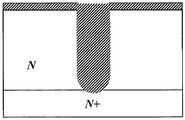
파워 MOSFET은 많은 전자 애플리케이션에서 스위칭 디바이스(switching device)로서 폭넓게 사용된다. 전도(conduction)와 스위칭 전력 손실을 최소화 하기 위해 소정의 절연파괴 전압을 위한 파워 MOSFET은 낮은 비(specific) 온-저항(low specific on-resistance) 및 커패시턴스(capacitances)를 가지는 것이 바람직하다. 비 온-저항(RSP)는 온-저항 영역 곱(RON*A)으로서 정의된다. 수퍼접합(SuperJunction)(SJ) 구조는 보다 높은 도핑 교번 p-타입 및 n-타입 층 또는 전하 균형이 이루어지는 필러들(pillars)을 병렬로 연결함으로써 낮은 비 온-저항을 달성한다. 따라서, SJ 구조에 대해, 보다 낮은 RSP로 소정의 단위 영역내에 많은 필러들 또는 셀들을 채워넣는 것이 바람직하다. Power MOSFETs are widely used as switching devices in many electronic applications. To minimize conduction and switching power dissipation, a power MOSFET for a given breakdown voltage preferably has a low specific on-resistance and capacitances. The on-resistance (R SP ) is defined as the on-resistance area product (R ON * A). The SuperJunction (SJ) structure achieves low on-resistance by connecting pillars with higher doping alternating p-type and n-type layers or charge balancing in parallel. Thus, for the SJ structure, it is desirable to fill many fillers or cells within a given unit area with a lower R SP .
SJ 구조에 있어서, n-타입 및 p-타입 필러의 최소 너비는 셀 피치 축소와 디바이스 스케일링에 대한 제한을 설정한다. 또한, 이러한 구조 제작과 관련된 여러 단점들이 존재하며, 연속적인 주입 및 확산 공정에 의해 결합된 다중 에피택셜 층(multiple epitaxial layers)을 성장시키기 위한 필요성을 포함한다. 부동 아일랜드(floating islands)를 채우거나 제공하는 에피택셜 트렌치(epitaxial trench)에 이어 트렌치를 형성하는 것과 같은 대안적인 해결책은 유사한 단점을 포함한다. 따라서, 보다 미세한 셀 피치로 스케일될 수 있는 낮은 RSP와 낮은 커패시턴스를 특징으로 하는 파워 MOS 트랜지스터를 위한 기술의 필요성이 있다. 추가적으로, 제조시 복잡함을 감소시키는 것이 바람직하다. In the SJ structure, the minimum widths of n-type and p-type fillers set limits for cell pitch reduction and device scaling. In addition, there are several disadvantages associated with fabricating such structures, including the need to grow multiple epitaxial layers coupled by a continuous implantation and diffusion process. An alternative solution, such as forming a trench following an epitaxial trench filling or providing floating islands, involves similar drawbacks. Thus, there is a need for a technique for a power MOS transistor featuring low R SP and low capacitance that can be scaled to finer cell pitches. In addition, it is desirable to reduce the complexity in manufacture.
본 발명의 실시예에 따르면, 일반적으로 전자공학 분야에 관련된 기법이 제공된다. 특히, 본 발명은 파워 MOS 트랜지스터 디바이스와 이 디바이스의 제조 방법에 관한 것이다. 단지 예로서, 발명은 드리프트 영역에서 전하 균형을 맞추는 고정 전하를 포함하는 파워 MOS 트랜지스터에 적용되었다. 특별한 실시예에서, 고정 전하는 하나 이상의 유전체 층내에 존재한다. 본 발명은 다른 MOS 구조와 마찬가지로 횡 및 수직 MOSFET 구조 모두에 적용할 수 있다.According to an embodiment of the present invention, techniques related to the field of electronics are generally provided. More particularly, the present invention relates to power MOS transistor devices and methods for fabricating the devices. By way of example only, the invention has been applied to a power MOS transistor comprising a fixed charge that balances the charge in the drift region. In a particular embodiment, the fixed charge is in one or more dielectric layers. The present invention is applicable to both lateral and vertical MOSFET structures as well as other MOS structures.
[기술적 해결방법][Technical Solution]
본 발명의 실시예에 따르면, 반도체 디바이스는 제 1 전도성 타입의 반도체 층과 제 1 전도성 타입의 반도체 층 위에 형성된 제 2 전도성 타입의 반도체 층을 포함한다. 제 2 전도성 타입의 반도체 층은 제 1 두께(first thickness)를 특징으로 한다. 반도체 디바이스는 또한 제 1 기설정된 거리(first predetermined distance)가 제 2 전도성 타입의 반도체 층까지 연장되는 바디 층(body layer)과 제 2 기설정된 거리가 제 2 전도성 타입의 반도체 층까지 연장되는 한 쌍의 트렌치를 포함한다. 각각의 한 쌍의 트렌치는 본질적으로 트첸치에 배치된 유전체 물질로 구성되고 제 2 전도성 타입의 반도체 층내에 존재하는 도핑 불순물의 농도와 한 쌍의 트렌치 사이의 거리는 반도체 디바이스의 전기적 특성을 정의한다. 반도체 디바이스는 상기 제 2 전도성 타입의 상기 반도체 층에 결합된 제어 게이트(control gate)와 상기 제 2 전도성 타입의 반도체 층에 결합된 소스 영역(source region)을 더 포함한다. According to an embodiment of the present invention, a semiconductor device includes a semiconductor layer of a first conductivity type and a semiconductor layer of a second conductivity type formed over the semiconductor layer of the first conductivity type. The second conductive type semiconductor layer is characterized by a first thickness. The semiconductor device may also include a body layer having a first predetermined distance extending to the semiconductor layer of the second conductivity type and a pair of body layers extending a second predetermined distance to the semiconductor layer of the second conductivity type. Lt; / RTI > Each pair of trenches consists essentially of a dielectric material disposed in the trenches and the concentration of doping impurities present in the semiconductor layer of the second conductivity type and the distance between the pair of trenches define the electrical characteristics of the semiconductor device. The semiconductor device further includes a control gate coupled to the semiconductor layer of the second conductivity type and a source region coupled to the semiconductor layer of the second conductivity type.
본 발명의 다른 실시예에 따르면, 반도체 디바이스는 제 1 전도성 타입의 반도체 층 및 제 1 전도성 타입의 반도체 층 위에 형성된 제 2 전도성 타입의 반도체 층을 포함한다. 제 2 전도성 타입의 반도체 층은 제 1 두께를 특징으로 한다. 반도체 디바이스는 또한 제 1 기설정된 거리가 제 2 전도성 타입의 반도체 층까지 연장되는 바디 층과 제 2 기설정된 거리가 제 2 전도성 타입의 반도체 층까지 연장되는 복수의 트렌치를 또한 포함한다. 각각의 복수의 트렌치는 트렌치 내에 배치된 제 1 유전체 물질을 포함하며 제 1 유전체 물질은 의도적으로 도입된 전하를 포함한다. 반도체 디바이스는 제 2 전도성 타입의 반도체에 결합된 복수의 제어 게이트와 제 2 전도성 타입의 반도체 층에 결합된 복수의 소스 영역을 더 포함한다. According to another embodiment of the present invention, a semiconductor device includes a semiconductor layer of a first conductivity type and a semiconductor layer of a second conductivity type formed over the semiconductor layer of a first conductivity type. The semiconductor layer of the second conductivity type is characterized by a first thickness. The semiconductor device also includes a body layer in which a first predetermined distance extends to the semiconductor layer of the second conductivity type and a plurality of trenches in which a second predetermined distance extends to the semiconductor layer of the second conductivity type. Each plurality of trenches comprises a first dielectric material disposed in the trench and the first dielectric material comprises intentionally introduced charge. The semiconductor device further includes a plurality of control gates coupled to the semiconductor of the second conductivity type and a plurality of source regions coupled to the semiconductor layer of the second conductivity type.
본 발명의 또 다른 실시예에 따라서, 반도체 디바이스는 제 1 전도성 타입의 반도체 층과 제 1 전도성 타입을 가지는 제 1 세트의 필러와 제 2 전도성 타입을 가지는 제 2 세트의 필러를 포함하는 반도체 층을 포함한다. 제 1 세트의 필러와 제 2 세트의 필러는 제 1 전도성 타입의 반도체 층에 형성된다. 제 1 세트의 필러와 제 2 세트의 필러는 제 1 두께를 특징으로 한다. 반도체 디바이스는 또한 기설정된 거리가 제 1 세트의 필러 또는 제 2 세트의 필러까지 연장되는 복수의 트렌치를 포함한다. 각각의 복수의 트렌치는 트렌치 내에 배치된 제 1 유전체 물질을 포함하며 제 1 유전체 물질은 의도적으로 도입된 전하를 포함한다. 반도체 디바이스는 제 1 세트의 필러와 제 2 세트의 필러를 포함하는 반도체 층에 결합된 복수의 제어 게이트와 제 1 세트의 필러와 제 2 세트의 필러를 포함하는 반도체 층에 결합된 복수의 소스 영역을 더 포함한다. According to another embodiment of the present invention, a semiconductor device includes a semiconductor layer comprising a first set of fillers having a first conductivity type, a first set of fillers having a first conductivity type, and a second set of fillers having a second conductivity type, . A first set of pillars and a second set of pillars are formed in the semiconductor layer of the first conductivity type. The first set of pillars and the second set of pillars are characterized by a first thickness. The semiconductor device also includes a plurality of trenches with predetermined distances extending to a first set of pillars or a second set of pillars. Each plurality of trenches comprises a first dielectric material disposed in the trench and the first dielectric material comprises intentionally introduced charge. A semiconductor device includes a plurality of source regions coupled to a semiconductor layer comprising a plurality of control gates coupled to a semiconductor layer comprising a first set of pillars and a second set of pillars, a first set of pillars and a second set of pillars, .
본 발명의 또 다른 실시예에 따라서, 반도체 디바이스는 제 1 전도성 타입의 반도체 층과 제 1 전도성 타입의 반도체 층에 형성된 제 2 전도성 타입의 반도체 층을 포함한다. 제 2 전도성 타입의 반도체 층은 제 1 두께를 특징으로 한다. 반도체 디바이스는 또한 기설정된 깊이를 갖고 제 2 전도성 타입의 반도체 층까지 연장됨으로써, 그에 의해 제 2 전도성 타입의 반도체 층과 트렌치 사이에 배치된 계면 영역(interfacial region)을 정의하는 트렌치를 포함한다. 트렌치는 본질적으로 트렌치 내에 배치된 유전체 물질로 구성되는 말단부(distal portion)와 트렌치의 인접부내 유전체 물질 내부에 배치된 게이트 물질(gate material)과 유전체 물질을 포함하는 인접부를 포함한다.According to another embodiment of the present invention, a semiconductor device includes a semiconductor layer of a first conductivity type and a semiconductor layer of a second conductivity type formed in a semiconductor layer of a first conductivity type. The semiconductor layer of the second conductivity type is characterized by a first thickness. The semiconductor device also includes a trench that has a predetermined depth and extends to a semiconductor layer of a second conductivity type thereby defining an interfacial region disposed between the semiconductor layer of the second conductivity type and the trench. The trench essentially comprises a distal portion comprising a dielectric material disposed within the trench and a proximal portion including a gate material and a dielectric material disposed within the dielectric material within the proximal portion of the trench.
반도체 디바이스는 기설정된 깊이를 갖고 제 2 전도성 타입의 반도체 층까지 연장됨으로써, 제 2 전도성 타입의 반도체 층과 제 2 트렌치 사이에 배치된 제 2 계면 영역을 정의하는 제 2 트렌치를 더 포함한다. 제 2 트렌치는 본질적으로 트렌치 내에 배치된 유전체 물질로 구성되는 말단부(distal portion)와 제 2 트렌치의 인접부내 유전체 물질 내부에 배치된 게이트 물질과 유전체 물질을 포함하는 인접부를 포함한다. 더욱이, 반도체 디바이스는 제 2 전도성 타입의 반도체 층에 결합된 소스 영역을 포함한다.The semiconductor device further includes a second trench defining a second interface region disposed between the second conductive type semiconductor layer and the second trench by extending to a semiconductor layer of a second conductivity type with a predetermined depth. The second trench essentially comprises a distal portion comprising a dielectric material disposed within the trench and a proximal portion including a gate material and a dielectric material disposed within the dielectric material within the vicinity of the second trench. Moreover, the semiconductor device includes a source region coupled to the semiconductor layer of the second conductivity type.
본 발명의 특정한 대안적인 실시예에 따라서, 반도체 디바이스는 제 2 전도성 타입의 반도체 층 위에 형성되는 제 1 전도성 타입의 반도체 층을 포함한다. 제 2 전도성 타입의 반도체 층은 제 1 두께를 특징으로 한다. 반도체 디바이스는 기설정된 깊이를 갖고 제 2 전도성 타입의 반도체 층까지 연장됨으로써, 제 2 전도성 타입의 반도체 층과 제 1 트렌치 사이에 배치된 제 1 계면 영역을 정의하는 제 1 트렌치를 포함한다. 제 1 트렌치는 본질적으로 트렌치 내에 배치된 유전체 물질로 구성되는 말단부(distal portion)및 유전체 물질과 트렌치의 인접부내 유전체 물질 내부에 배치된 게이트 물질을 포함하는 인접부를 포함한다. 의도적으로 도입된 전하는 제 1 트렌치의 말단부 또는 제 1 계면 영역에 배치된 유전체 물질 중 적어도 하나에 제공된다. According to a particular alternative embodiment of the present invention, a semiconductor device comprises a semiconductor layer of a first conductivity type formed over a semiconductor layer of a second conductivity type. The semiconductor layer of the second conductivity type is characterized by a first thickness. The semiconductor device includes a first trench having a predetermined depth and extending to a semiconductor layer of a second conductivity type thereby defining a first interface region disposed between the semiconductor layer of the second conductivity type and the first trench. The first trench essentially comprises a distal portion comprising a dielectric material disposed within the trench and a proximal portion including a dielectric material and a gate material disposed within the dielectric material within the proximal portion of the trench. Intentionally introduced charge is provided to at least one of the dielectric material disposed at the distal end of the first trench or the first interface region.
반도체 디바이스는 또한 기설정된 깊이를 갖고 제 2 전도성 타입의 반도체 층까지 연장됨으로써, 제 2 전도성 타입의 반도체 층과 제 2 트렌치 사이에 배치된 제 2 계면 영역을 정의하는 제 2 트렌치를 포함한다. 제 2 트렌치는 본질적으로 트렌치 내에 배치된 유전체 물질로 구성되는 말단부(distal portion)와 제 2 트렌치의 인접부내 유전체 물질 내부에 배치된 유전체 물질과 게이트 물질을 포함하는 인접부를 포함한다. 의도적으로 도입된 전하는 제 2 트렌치의 말단부 또는 제 2 계면 영역에 배치된 유전체 물질 중 적어도 하나에 제공된다.The semiconductor device also includes a second trench that defines a second interface region disposed between the second conductive type semiconductor layer and the second trench by extending to a semiconductor layer of a second conductivity type with a predetermined depth. The second trench essentially comprises a distal portion comprised of a dielectric material disposed within the trench and a proximal portion comprising a dielectric material and gate material disposed within the dielectric material within the vicinity of the second trench. Intentionally introduced charge is provided to at least one of the dielectric material disposed at the distal end of the second trench or the second interface region.
본 발명의 또 다른 대안적인 실시예에 따라서, 반도체 디바이스는 제 1 표면과 제 2 표면, 제 1 표면상에 배치된 소스 영역, 그리고 소스 영역과 인접한 제 1 표면상에 배치된 게이트 영역을 가지는 제 1 전도성 타입의 반도체 층을 포함한다. 반도체 디바이스는 또한 제 1 표면상에 배치된 드레인 영역(drain region)과 게이트 영역과 드레인 영역 사이에 배치된 한 쌍의 전하 제어 트렌치를 포함한다. 각각의 한 쌍의 전하 제어 트렌치는 너비를 특징으로 하며 트렌치 내에 배치된 제 1 유전체 물질과 제 1 유전체 물질 내부에 배치된 제 2 물질을 포함한다. 제 1 전도성 타입의 반도체 층내에 존재하는 도핑 불순물의 농도와 한 쌍의 전하 제어 트렌치 사이의 거리는 각각의 한 쌍의 전하 제어 트렌치의 너비의 독립적인 반도체 디바이스의 전기적 특성을 정의한다. 반도체 디바이스는 제 1 전도성 타입의 반도체 층에 결합된 제어 게이트와 제 1 전도성 타입의 반도체 층에 결합된 소스 영역을 더 포함한다.According to yet another alternative embodiment of the present invention, a semiconductor device includes a semiconductor device having a first surface and a second surface, a source region disposed on the first surface, and a gate region disposed on the first surface adjacent the source region, 1 < / RTI > conductive type semiconductor layer. The semiconductor device also includes a drain region disposed on the first surface and a pair of charge control trenches disposed between the gate region and the drain region. Each pair of charge control trenches is characterized by a width and includes a first dielectric material disposed within the trench and a second material disposed within the first dielectric material. The concentration of doping impurities present in the semiconductor layer of the first conductivity type and the distance between the pair of charge control trenches define the electrical characteristics of the semiconductor device independent of the width of each pair of charge control trenches. The semiconductor device further includes a control gate coupled to the semiconductor layer of the first conductivity type and a source region coupled to the semiconductor layer of the first conductivity type.
본 발명의 또 다른 대안적인 실시예에 따라서, 제 1 표면과 제 2 표면, 제 1 표면위에 배치된 소스 영역, 그리고 소스 영역에 인접한 제 1 표면위에 배치된 게이트 영역을 가지는 제 1 전도성 타입의 반도체 층을 포함한다. 반도체 디바이스는 또한 제 1 표면 위에 배치된 드레인 영역과 게이트 영역과 드레인 영역 사이에 배치된 전하 제어 트렌치를 포함한다. 전하 제어 트렌치는 트렌치 내에 배치된 제 1 유전체 물질을 포함한다. 제 1 유전체 물질은 의도적으로 도입된 전하를 포함한다. According to yet another alternative embodiment of the present invention there is provided a semiconductor device comprising a first conductive type semiconductor having a first surface and a second surface, a source region disposed over the first surface, and a gate region disposed over the first surface adjacent the source region, Layer. The semiconductor device also includes a drain region disposed over the first surface and a charge control trench disposed between the gate region and the drain region. The charge control trench includes a first dielectric material disposed within the trench. The first dielectric material includes intentionally introduced charge.
본 발명의 특별한 실시예에 따라서, 반도체 디바이스는 제 1 전도성 타입의 반도체 층을 포함한다. 제 1 전도성 타입의 반도체 층은 반도체 층 위에 형성된 제 2 전도성 타입의 제 1 반도체 영역을 포함한다. 제 1 반도체 영역은 제 1 두께를 특징으로 한다. 제 1 반도체 영역은 기설정된 깊이를 갖고 제 1 반도체 영역까지 연장됨으로써, 제 1 반도체 영역과 제 1 트렌치 사이에 배치된 제 1 계면 영역을 정의하는 제 1 트렌치를 포함한다. 제 1 트렌치는 제 1 트렌치의 인접부와 제 1 트렌치의 말단부에 배치된 제 1 유전체 물질을 포함한다. 의도적으로 도입된 전하는 제 1 트렌치의 인접부와 제 1 계면 영역내에 배치된 제 1 유전체 물질 중 적어도 하나에 존재한다. 제 1 트렌치는 또한 제 1 트렌치의 인접부내 제 1 유전체 물질 내부에 배치된 제 1 게이트 물질을 포함한다. According to a particular embodiment of the invention, the semiconductor device comprises a semiconductor layer of a first conductivity type. The first conductive type semiconductor layer includes a first semiconductor region of a second conductivity type formed over the semiconductor layer. The first semiconductor region is characterized by a first thickness. The first semiconductor region includes a first trench having a predetermined depth and extending to the first semiconductor region, thereby defining a first interface region disposed between the first semiconductor region and the first trench. The first trench includes a first dielectric material disposed at a proximal portion of the first trench and at a distal end of the first trench. Intentionally introduced charge is present in at least one of a proximity of the first trench and a first dielectric material disposed in the first interface region. The first trench also includes a first gate material disposed within the first dielectric material within the proximity of the first trench.
제 1 전도성 타입의 반도체 층은 또한 반도체 위에 형성된 제 1 전도성 타입의 제 2 반도체 영역을 포함한다. 제 2 반도체 영역은 제 2 두께를 특징으로 한다. 제 2 반도체 영역은 제 2 기설정된 깊이를 갖고 제 2 반도체 영역까지 연장됨으로써, 제 2 반도체 영역과 제 2 트렌치 사이에 배치된 제 2 계면 영역을 정의하는 제 2 트렌치를 포함한다. 제 2 트렌치는 제 2 트렌치의 인접부와 제 2 트렌치의 말단부내에 배치된 제 2 유전체 물질을 포함한다. 의도적으로 도입된 전하는 제 2 트렌치의 인접부 또는 제 2 계면 영역내에 배치된 제 2 유전체 물질 중 적어도 하나에 제공된다. 제 2 트렌치는 또한 제 2 트렌치의 인접부내 제 2 유전체 물질 내부에 배치된 제 2 게이트 물질을 포함한다. The first conductive type semiconductor layer also includes a second semiconductor region of a first conductivity type formed over the semiconductor. The second semiconductor region is characterized by a second thickness. The second semiconductor region includes a second trench having a second predetermined depth and extending to the second semiconductor region, thereby defining a second interface region disposed between the second semiconductor region and the second trench. The second trench includes a second dielectric material disposed within a proximal portion of the second trench and a distal portion of the second trench. Intentionally introduced charge is provided to at least one of the adjacent portions of the second trench or the second dielectric material disposed in the second interface region. The second trench also includes a second gate material disposed within the second dielectric material in the vicinity of the second trench.
본 발명의 또 다른 특별한 실시예에 따라서, 반도체 디바이스를 제조하는 방법이 제공된다. 방법은 제 1 전도성 타입의 반도체 층을 제공하는 단계, 제 1 전도성 타입의 반도체 층 위에 제 2 전도성 타입의 반도체 층을 형성하는 단계, 제 2 전도성 타입의 반도체층 위에 하나 이상의 절연 층(insulator layers)을 형성하는 단계, 그리고 제 2 전도성 타입의 반도체 층내 복수의 트렌치를 에칭함으로써, 복수의 CC 트렌치와 CG 트렌치를 형성하는 단계를 포함한다. 방법은 또한 복수의 트렌치와 제 2 전도성 타입의 반도체 층 위에 산화물 층을 형성하는 단계, 하나 이상의 절연 층의 일부에 마스킹 층(masking layer)을 형성하는 단계, CG 트렌치에 게이트 산화물 층(gate oxide layer)을 형성하는 단계, 그리고 CG 트렌치에 폴리실리콘 게이트 물질을 형성하는 단계를 포함한다. 방법은 제 2 절연 층을 형성함으로써, CC 트렌치의 일부를 채우는 단계, 제 2 물질을 형성함으로써, CC 트렌치의 제 2 부분을 채우는 단계, 그리고 제 3 절연 층을 형성함으로써, CC 트렌치의 CC의 나머지(remainder)를 채우는 단계를 더 포함한다. 더욱이, 방법은 하나 이상의 디바이스 영역을 형성하는 단계와 소스 금속 층(source metal layer)을 형성하는 단계를 포함한다.According to yet another particular embodiment of the present invention, a method of manufacturing a semiconductor device is provided. The method includes providing a semiconductor layer of a first conductivity type, forming a second conductive type semiconductor layer over the first conductive type semiconductor layer, forming one or more insulator layers over the second conductive type semiconductor layer, And etching the plurality of trenches in the second conductive type semiconductor layer to form a plurality of CC trenches and CG trenches. The method also includes forming an oxide layer over the plurality of trenches and the second conductive type semiconductor layer, forming a masking layer on a portion of the at least one insulating layer, forming a gate oxide layer ), And forming a polysilicon gate material in the CG trench. The method includes filling a portion of a CC trench by forming a second insulating layer, filling a second portion of the CC trench by forming a second material, and forming a third insulating layer, and filling the remainder. Moreover, the method includes forming at least one device region and forming a source metal layer.
본 발명의 또 다른 특별한 실시예에 따라서, 반도체 디바이스 제조 방법이 제공된다. 방법은 제 1 전도성 타입의 반도체 층을 제공하는 단계, 제 1 전도성 타입의 반도체 층 위에 제 2 전도성 타입의 반도체 층을 형성하는 단계, 제 2 전도성 타입의 반도체 층 위에 절연 층을 형성하는 단계, 그리고 제 2 전도성 타입의 적어도 반도체 층까지 트렌치를 에칭하는 단계를 포함한다. 방법은 또한 트렌치와 제 2 전도성 타입의 반도체 층 위에 열적 산화물 층(thermal oxide layer)을 형성하는 단계, 열적 산화물 층내로 이온을 주입하는 단계, 제 2 절연 층을 형성함으로써, 트렌치의 적어도 일부를 채우는 단계, 그리고 트렌치의 일부로부터 제 2 절연 층을 제거하는 단계를 포함한다. 방법은 트렌치와 에피택셜 층 위에 산화물 층을 형성하는 단계, 트렌치에 물질을 형성하는 단계, 하나 이상의 디바이스 영역을 형성하는 단계, 그리고 게이트 물질 위에 제 2 게이트 산화물 층을 형성하는 단계를 더 포함한다. 더욱이, 방법은 제 2 게이트 산화물 층을 패턴화하는 단계 및 소스 금속 층(source metal layer)을 형성하는 단계를 포함한다. According to another specific embodiment of the present invention, a method of manufacturing a semiconductor device is provided. The method includes providing a semiconductor layer of a first conductivity type, forming a semiconductor layer of a second conductivity type over the semiconductor layer of the first conductivity type, forming an insulating layer over the semiconductor layer of the second conductivity type, Etching the trench to at least the semiconductor layer of the second conductivity type. The method also includes forming a thermal oxide layer over the trench and the second conductive type semiconductor layer, implanting ions into the thermal oxide layer, forming a second insulating layer, filling at least a portion of the trench, And removing the second insulating layer from a portion of the trench. The method further includes forming an oxide layer over the trench and the epitaxial layer, forming a material in the trench, forming at least one device region, and forming a second gate oxide layer over the gate material. Moreover, the method includes patterning the second gate oxide layer and forming a source metal layer.
본 발명의 특정한 실시예에 따라서, 반도체 디바이스를 제조하는 방법이 제공된다. 방법은 제 1 전도성 타입의 반도체 층을 제공하는 단계, 제 1 전도성 타입의 반도체 층 위에 제 2 전도성 타입의 반도체 층을 형성하는 단계, 제 2 전도성 타입의 적어도 반도체 층까지 트렌치를 에칭하는 단계, 그리고 트렌치 내 제 1 절연층을 형성하는 단계를 포함한다. 방법은 또한 제 2 절연 층을 형성함으로써, CC 트렌치의 적어도 일부를 채우는 단계 및 트렌치에 게이트 물질을 형성하는 단계를 포함한다. 방법은 하나 이상의 디바이스 영역을 형성하고 소스 금속 층을 형성하는 단계를 포함한다. According to a particular embodiment of the present invention, a method of manufacturing a semiconductor device is provided. The method includes providing a semiconductor layer of a first conductivity type, forming a semiconductor layer of a second conductivity type over the semiconductor layer of the first conductivity type, etching the trench to a semiconductor layer of at least a second conductivity type, And forming a first insulating layer in the trench. The method also includes filling at least a portion of the CC trench by forming a second insulating layer, and forming a gate material in the trench. The method includes forming at least one device region and forming a source metal layer.
본 발명의 다른 특정한 실시예에 따라서, 반도체 디바이스를 제조하는 방법이 제공된다. 방법은 제 1 전도성 타입의 반도체 층을 제공하는 단계, 제 1 전도성 타입의 반도체 층 위에 제 2 전도성 타입의 반도체 층을 형성하는 단계, 제 2 전도성 타입의 반도체 층 위에 절연 층을 형성하는 단계, 그리고 제 2 전도성 타입의 적어도 반도체 층까지 하나 이상의 트렌치를 에칭하는 단계를 포함한다. 방법은 또한 하나 이상의 트렌치에 제 2 절연 층을 형성하는 단계, 제 2 절연 층내로 이온을 주입하는 단계, 제 3 절연 층을 형성함으로써, 하나 이상의 트렌치의 적어도 일부를 채우는 단계, 그리고 제 2 전도성 타입의 적어도 반도체 층까지 추가적인 트렌치(additional trench)를 에칭하는 단계를 포함한다. 방법은 추가적인 트렌치에 게이트 산화물 층을 형성하는 단계, 추가적인 트렌치에 게이트 물질을 형성하는 단계, 하나 이상의 디바이스 영역을 형성하는 단계, 그리고 소스 금속 층을 형성하는 단계를 더 포함한다. According to another specific embodiment of the present invention, a method of manufacturing a semiconductor device is provided. The method includes providing a semiconductor layer of a first conductivity type, forming a semiconductor layer of a second conductivity type over the semiconductor layer of the first conductivity type, forming an insulating layer over the semiconductor layer of the second conductivity type, Etching at least one trench to at least the semiconductor layer of the second conductivity type. The method also includes forming a second insulating layer over the at least one trench, implanting ions into the second insulating layer, filling at least a portion of the at least one trench by forming a third insulating layer, And etching additional trenches to at least the semiconductor layer of the semiconductor substrate. The method further comprises forming a gate oxide layer in the additional trench, forming a gate material in the additional trench, forming one or more device regions, and forming a source metal layer.
본 발명의 또 다른 특정한 실시예에 따라서, 반도체 디바이스를 제조하는 방법이 제공된다. 방법은 제 1 전도성 타입의 반도체 층을 제공하는 단계, 제 1 전도성 타입의 반도체 층 위에 제 2 전도성 타입의 반도체 층을 형성하는 단계, 그리고 제 2 전도성 타입의 반도체 층 위에 절연 층을 형성하는 단계를 포함한다. 방법은 또한 제 2 전도성 타입의 적어도 반도체 층까지 트렌치를 에칭하는 단계, 트렌치 내와 제 2 전도성 타입의 반도체 층 위에 산화물 층을 형성하는 단계, 그리고 산화물 층내로 이온을 주입하는 단계를 포함한다. 방법은 제 2 절연 층을 형성함으로써, 트렌치를 채우는 단계, 하나 이상의 디바이스 영역을 형성하는 단계, 그리고 금속 층을 형성하는 단계를 더 포함한다. According to another specific embodiment of the present invention, a method of manufacturing a semiconductor device is provided. The method includes providing a first conductive type semiconductor layer, forming a second conductive type semiconductor layer over the first conductive type semiconductor layer, and forming an insulating layer over the second conductive type semiconductor layer . The method also includes etching the trench to at least the semiconductor layer of the second conductivity type, forming an oxide layer in the trench and on the semiconductor layer of the second conductivity type, and implanting ions into the oxide layer. The method further comprises filling the trench, forming one or more device regions, and forming a metal layer by forming a second insulating layer.
본 발명을 이용함으로써 종래의 기법에 비해 수많은 장점들이 달성된다. 예를 들어, 본 발명에 따른 실시예에서, 개선된 MOSFET 전도 및 퍼포먼스 스위칭이 달성된다. 더욱이, 다른 실시예에서, 교번 전하 균형 유전 및 실리콘 층을 나란히 함으로써 소정의 도핑 농도에 대한 1차원 실리콘 절연파괴 전압 한계를 초과하는 성능을 디바이스에 제공한다. 고정 전하의 사용은 p-n 접합이 전하 균형 목적을 위해 사용되는 종래의 기법에 비해 커패시턴스를 감소시킨다. 더욱이, 리버스 복구 전하(reverse recovery charge: Qrr)와 안전 작동 영역(Safe Operating Area: SOA)이 종래의 디바이스에 비해 개선된다. 실시예에 따라서, 하나 이상의 이들 잇점이 존재할 수 있다. 이들 및 다른 잇점들은 본 발명의 명세서의 도처에 그리고 특히 아래에 기술되었다. 본 발명의 다양한 추가적인 목적, 특징 및 장점들이 상세한 설명과 다음의 첨부 도면을 참조하여 보다 충분히 이해될 수 있다.Numerous advantages are achieved by using the present invention over conventional techniques. For example, in embodiments in accordance with the present invention, improved MOSFET conduction and performance switching is achieved. Moreover, in another embodiment, the alternating charge balance dielectric and silicon layers are arranged side by side to provide a device with performance that exceeds the one-dimensional silicon dielectric breakdown voltage limit for a given doping concentration. The use of a fixed charge reduces the capacitance compared to conventional techniques where a pn junction is used for charge balancing purposes. Moreover, reverse recovery charge (Q rr ) and safe operating area (SOA) are improved compared to conventional devices. Depending on the embodiment, there may be one or more of these advantages. These and other advantages are described all over the specification of the present invention and in particular below. Various further objects, features and advantages of the present invention can be more fully understood by reference to the following detailed description and the accompanying drawings.
도 1A는 본 발명의 실시예에 따른 평면 n-채널 DMOS 트랜지스터(planar n-channel DMOS transistor)의 단순 예시도;FIG. 1A is a simplified illustration of a planar n-channel DMOS transistor according to an embodiment of the present invention; FIG.
도 1B는 본 발명의 실시예에 따른 트렌치 n-채널 MOS 트랜지스터(trench n-channel DMOS transistor)의 단순 예시도;1B is a simplified illustration of a trench n-channel DMOS transistor according to an embodiment of the present invention;
도 2A는 본 발명의 실시예에 따른 제 2 유전체 물질을 포함하는 전하 제어 트렌치(Charge Control trenches)를 가지는 트렌치 MOS 트랜지스터의 단순 예시도;FIG. 2A is a simplified illustration of a trench MOS transistor having charge control trenches including a second dielectric material in accordance with an embodiment of the present invention; FIG.
도 2B는 본 발명의 실시예에 따른 제 2 유전체 물질과 보이드(void)를 포함하는 전하 제어 트렌치(Charge Control trenches)를 가지는 트렌치 MOS 트랜지스터의 단순 예시도;Figure 2B is a simplified illustration of a trench MOS transistor having charge control trenches including a second dielectric material and a void in accordance with an embodiment of the present invention;
도 3A는 본 발명의 실시예에 따른 동일한 트렌치에 제공된 제어 게이트와 전 하 제어를 가지는 트렌치 MOS 트랜지스터의 단순 예시도;3A is a simple example of a trench MOS transistor having a control gate and charge control provided in the same trench according to an embodiment of the present invention;
도 3B는 본 발명의 다른 실시예에 따른 동일한 트렌치에 제공된 제어 게이트와 전하 제어를 가지는 트렌치 MOS 트랜지스터의 단순 예시도;3B is a simplified illustration of a trench MOS transistor having a control gate and charge control provided in the same trench according to another embodiment of the present invention;
도 4는 본 발명의 실시예에 따른 딥 p+층(deep p+layer)을 가지는 제어 게이트 트렌치와 전하 제어 트렌치를 가지는 트렌치 MOS 트랜지스터의 단순 예시도;4 is a simplified illustration of a trench MOS transistor having a control gate trench and a charge control trench having a deep p + layer according to an embodiment of the present invention;
도 5는 본 발명의 실시예에 따른 제 1 유전체 물질에 의해 커버된 제어 게이트 트렌치와 전하 제어 트렌치를 가지는 트렌치 MOS 트랜지스터의 단순 예시도;5 is a simple illustration of a trench MOS transistor having a control gate trench and a charge control trench covered by a first dielectric material in accordance with an embodiment of the present invention;
도 6은 본 발명의 실시예에 따른 제 1 유전체 물질에 의해 커버된 제어 게이트 트렌치와 전하 제어 트렌치 모두를 가지는 트렌치 MOS 트랜지스터의 단순 예시도;6 is a simplified illustration of a trench MOS transistor having both a control gate trench and a charge control trench covered by a first dielectric material in accordance with an embodiment of the present invention;
도 7은 본 발명의 실시예에 따른 두꺼운 하부 산화물 및 전하 제어 트렌치를 가지는 제어 게이트 트렌치를 가지는 트렌치 MOS 트랜지스터의 단순 예시도;7 is a simplified illustration of a trench MOS transistor having a control gate trench having a thick bottom oxide and charge control trench in accordance with an embodiment of the present invention;
도 8은 본 발명의 실시예에 따른 n 드리프트 영역까지 연장되는 두꺼운 하부 산화물 및 전하 제어 트렌치를 가지는 제어 게이트 트렌치를 가지는 트렌치 MOS 트랜지스터의 단순 예시도;Figure 8 is a simple illustration of a trench MOS transistor having a control gate trench with a thick bottom oxide and charge control trench extending to an n drift region according to an embodiment of the present invention;
도 9는 본 발명의 실시예에 따른 n-에피택셜 층의 두께보다 작은 깊이를 가지는 계단형 게이트 산화물 제어 게이트와 전하 제어 트렌치를 가지는 트렌치 MOS 트랜지스터의 단순 예시도;9 is a simple illustration of a trench gate oxide control gate having a depth less than the thickness of the n-epitaxial layer and a trench MOS transistor having a charge control trench in accordance with an embodiment of the present invention;
도 10은 본 발명의 실시예에 따른 동일한 깊이를 가지는 균일한 산화물 제어 게이트 및 CC 트렌치를 가지는 트렌치 MOS 트랜지스터의 단순 예시도;10 is a simplified illustration of a trench MOS transistor having a uniform oxide control gate and a CC trench having the same depth according to an embodiment of the present invention;
도 11은 본 발명의 실시예에 따른 동일한 깊이를 가지는 두꺼운 하부 산화물 제어 게이트 및 CC 트렌치를 가지는 트렌치 MOS 트랜지스터의 단순 예시도;11 is a simple illustration of a trench MOS transistor having a thick bottom oxide control gate and a CC trench having the same depth according to an embodiment of the present invention;
도 12A는 본 발명의 실시예에 따른 파워 MOSFET 구조의 단순 평면 예시도;12A is a simplified plan view of a power MOSFET structure in accordance with an embodiment of the present invention;
도 12B는 도 12A의 라인(AA')을 따라서 바라본 단순 단면 예시도;FIG. 12B is a simplified cross-sectional exemplary view along line AA 'of FIG. 12A; FIG.
도 12C는 도 12A의 라인(BB')을 따라서 바라본 단순 단면 예시도;FIG. 12C is a simplified cross-sectional exemplary view along line BB 'of FIG. 12A; FIG.
도 13은 본 발명의 실시예에 따른 제어 게이트와 전하 제어 트렌치를 가지는 준-수직(quasi-vertical) 파워 MOSFET의 싱글 셀(single cell)의 단순 예시도;Figure 13 is a simple illustration of a single cell of a quasi-vertical power MOSFET having a control gate and charge control trenches in accordance with an embodiment of the present invention;
도 14A는 본 발명의 실시예에 따른 전하 제어 트렌치와 두꺼운 하부 산화물 제어 게이트 트렌치 및 제 1 유전체 물질로 충진된 터미네이션 트렌치를 가지는 준-수직(quasi-vertical) 파워 MOSFET 구성의 단순 예시도;14A is a simplified illustration of a quasi-vertical power MOSFET configuration having a charge control trench, a thick bottom oxide control gate trench, and a termination trench filled with a first dielectric material, in accordance with an embodiment of the present invention;
도 14B는 본 발명의 실시예에 따른 두꺼운 하부 산화물 제어 게이트, 전하 제어 트렌치 및 제 1 유전체 물질로 충진된 터미네이션 트렌치와 동일한 깊이를 가지는 전하 제어 트렌치와 두꺼운 하부 산화물 제어 게이트 트렌치 및 제 1 유전체 물질로 충진된 터미네이션 트렌치를 가지는 준-수직(quasi-vertical) 파워 MOSFET 구성의 단순 예시도;14B is a cross-sectional view of a portion of a charge control trench having the same depth as a termination trench filled with a charge control trench and a first dielectric material, a thick lower oxide control gate trench and a first dielectric material A simple example of a quasi-vertical power MOSFET configuration with a filled termination trench;
도 15A는 본 발명의 실시예에 따른 횡적 파워 MOSFET 구조의 단순 평면 예시도;15A is a simplified plan view of a transverse power MOSFET structure in accordance with an embodiment of the present invention;
도 15B는 도 15A의 라인(AA')을 따라서 바라본 단순 단면 예시도;FIG. 15B is a simplified cross-sectional exemplary view along line AA 'of FIG. 15A; FIG.
도 15C는 도 15A의 라인(BB')을 따라서 바라본 단순 단면 예시도;FIG. 15C is a simplified cross-sectional exemplary view along line BB 'of FIG. 15A; FIG.
도 15D는 도 15A의 라인(CC')을 따라서 바라본 단순 단면 예시도;FIG. 15D is a simplified cross-sectional exemplary view along line CC 'of FIG. 15A; FIG.
도 16은 본 발명의 실시예에 따른 전하 제어 트렌치가 충진된 유전체 층에 위치된 포지티브 전하를 가지는 n-채널 트렌치 MOS 트랜지스터의 단순 예시도;Figure 16 is a simplified illustration of an n-channel trench MOS transistor having a positive charge located in a dielectric layer filled with charge control trenches in accordance with an embodiment of the present invention;
도 17A는 본 발명의 실시예에 따른 전하 제어 트렌치와 p-바디 영역이 충진된 유전체 층을 포함하는 포지티브 전하를 가지는 n-채널 트렌치 MOS 트랜지스터의 단순 예시도;17A is a simple illustration of an n-channel trench MOS transistor having a positive charge including a charge control trench and a dielectric layer filled with a p-body region in accordance with an embodiment of the present invention;
도 17B는 본 발명의 실시예에 따른 전하 제어 트렌치가 충진된 유전체 층을 포함하는 포지티브 전하를 가지는 조합된 수퍼접합 트렌치 MOS 트랜지스터의 단순 예시도;17B is a simplified illustration of a combined super junction trench MOS transistor having a positive charge including a dielectric layer filled with charge control trenches in accordance with an embodiment of the present invention;
도 18A는 본 발명의 실시예에 따른 트렌치 위에 유전체 층을 가지는 도 17a에 예시된 바와 같은 트렌치 MOS 트랜지스터의 단순 예시도;Figure 18A is a simple illustration of a trench MOS transistor as illustrated in Figure 17A having a dielectric layer over a trench in accordance with an embodiment of the present invention;
도 18B는 본 발명의 실시예에 따른 트렌치에 추가적인 유전체 층을 가지는 도 18A에 예시된 바와 같은 트렌치 MOS 트랜지스터의 단순 예시도;Figure 18B is a simple illustration of a trench MOS transistor as illustrated in Figure 18A with a further dielectric layer in the trench according to an embodiment of the present invention;
도 18C는 본 발명의 실시예에 따른 트렌치와 제어 게이트 물질에 인접한 추가적인 유전체 층을 가지는 도 18A에 예시된 바와 같은 트렌치 MOS 트랜지스터의 단순 예시도;18C is a simplified illustration of a trench MOS transistor as illustrated in FIG. 18A having additional dielectric layers adjacent to the trench and control gate material in accordance with an embodiment of the present invention;
도 19는 본 발명의 실시예에 따른 n-드리프트 영역까지 연장되는 트렌치 깊이(trench depth)를 가지는 도 20에 도시된 바와 같은 트렌치 DMOS 트랜지스터의 단순 예시도;Figure 19 is a simple illustration of a trench DMOS transistor as shown in Figure 20 having a trench depth extending to an n-drift region according to an embodiment of the present invention;
도 20은 본 발명의 실시예에 따른 p- 영역과 기판 사이에 n-드리프트 영역을 가지는 도 17A에 예시된 바와 같은 트렌치 MOS 트랜지스터의 단순 예시도;Figure 20 is a simple illustration of a trench MOS transistor as illustrated in Figure 17A having an n-drift region between a p-region and a substrate in accordance with an embodiment of the present invention;
도 21A는 본 발명의 실시예에 따른 계단형 게이트 산화물을 가지는 도 18에 도시된 바와 같은 트렌치 MOS 트랜지스터의 단순 예시도;Figure 21A is a simple illustration of a trench MOS transistor as shown in Figure 18 with a stepped gate oxide according to an embodiment of the present invention;
도 21B는 본 발명의 실시예에 따른 계단형 게이트 산화물을 가지는 도 20에 예시된 바와 같은 트렌치 MOS 트랜지스터의 단순 예시도;Figure 21B is a simple illustration of a trench MOS transistor as illustrated in Figure 20 with a stepped gate oxide according to an embodiment of the present invention;
도 22A는 본 발명의 실시예에 따른 디바이스 터미네이션을 위해 트렌치를 채우는 유전체를 가지는 도 20에 도시된 바와 같은 트렌치 MOS 트랜지스터의 단순 예시도;22A is a simplified illustration of a trench MOS transistor as shown in FIG. 20 having a dielectric filling the trench for device termination in accordance with an embodiment of the present invention;
도 22B는 본 발명의 실시예에 따른 디바이스의 에지에 n+ 영역과 p- 영역 단 접점을 가지는 디바이스 터미네이션을 위해 트렌치를 채우는 유전체를 가지는 도 20에 예시된 바와 같은 트렌치 MOS 트랜지스터의 단순 예시도;Figure 22B is a simple illustration of a trench MOS transistor as illustrated in Figure 20 having a dielectric filling the trench for device termination having an n + region and a p-region shorting point at the edge of the device according to an embodiment of the present invention;
도 23A는 본 발명의 실시예에 따른 n+ 영역과 p+ 영역의 대안적인 레이아웃(alternative layout)을 가지는 도 18A에 예시된 바와 같은 파워 MOSFET 구조의 단순 평면 예시도;23A is a simplified plan view of a power MOSFET structure as illustrated in FIG. 18A having an alternative layout of an n + region and a p + region according to an embodiment of the present invention;
도 23B는 도 23A의 라인(AA')을 따라서 바라본 단순 단면 예시도;FIG. 23B is a simplified cross-sectional exemplary view along line AA 'of FIG. 23A; FIG.
도 23C는 도 23A의 라인(BB')을 따라서 바라본 단순 단면 예시도;Figure 23C is a simplified cross-sectional exemplary view along line BB 'of Figure 23A;
도 24는 본 발명의 실시예에 따른 종래의 터미네이션 구조를 가지는 준-수직 파워 MOSFET 구성의 단순 예시도;24 is a simplified illustration of a quasi-vertical power MOSFET configuration having a conventional termination structure in accordance with an embodiment of the present invention;
도 25는 본 발명의 실시예에 따른 터미네이션을 위해 트렌치를 채우는 유전체 물질을 이용한 준-수직 파워 MOSFET 구성의 단순 예시도;Figure 25 is a simple illustration of a quasi-vertical power MOSFET configuration using a dielectric material filling the trenches for termination according to an embodiment of the present invention;
도 26A는 본 발명의 대안적인 실시예에 따른 횡적 파워 MOSFET 구조의 단순 평면 예시도;26A is a simplified plan view of a transverse power MOSFET structure in accordance with an alternative embodiment of the present invention;
도 26B는 도 26A의 라인(AA')을 따라서 바라본 단순 단면 예시도;FIG. 26B is a simplified cross-sectional exemplary view along line AA 'of FIG. 26A; FIG.
도 26C는 도 26A의 라인(AA')을 따라서 바라본 단순한 대안적인 단면 예시도;Fig. 26C is a simple alternative cross-sectional illustration as viewed along line AA 'in Fig. 26A; Fig.
도 26D는 도 26A의 라인(AA')을 따라서 바라본 단순한 대안적인 단면 예시도;Figure 26D is a simple alternative cross-sectional view along line AA 'of Figure 26A;
도 26E는 도 26A의 라인(BB')을 따라서 바라본 단순 단면 예시도;Figure 26E is a simplified cross-sectional exemplary view along line BB 'of Figure 26A;
도 26F는 본 발명의 대안적인 실시예에 따른 횡적 파워 MOSFET 구조의 단순 단면 예시도;Figure 26F is a simplified cross-sectional illustration of a transverse power MOSFET structure in accordance with an alternative embodiment of the present invention;
도 26G는 본 발명의 다른 대안적인 실시예에 따른 횡적 파워 MOSFET 구조의 단순 단면 예시도;Figure 26G is a simplified cross-sectional illustration of a transverse power MOSFET structure in accordance with another alternative embodiment of the present invention;
도 26H는 본 발명의 대안적인 실시예에 따른 횡적 파워 MOSFET 구조의 단순 평면 예시도;Figure 26H is a simplified plan view of a transverse power MOSFET structure in accordance with an alternative embodiment of the present invention;
도 26I는 본 발명의 다른 대안적인 실시예에 따른 횡적 파워 MOSFET 구조의 단순 평면 예시도;Figure 26I is a simplified plan view of a transverse power MOSFET structure in accordance with another alternative embodiment of the present invention;
도 26J는 도 26I의 라인(AA')을 따라서 바라본 단순 단면 예시도;Figure 26J is a simplified cross-sectional exemplary view along line AA 'of Figure 26I;
도 26K는 도 26I의 라인(BB')을 따라서 바라본 단순 단면 예시도;Figure 26K is a simplified cross-sectional exemplary view along line BB 'of Figure 26I;
도 27A는 본 발명의 실시예에 따른 전하 제어 트렌치를 채우는 유전체 층 및 제어 게이트 트렌치를 가지는 p-채널 트렌치 MOS 트랜지스터의 단순 예시도;Figure 27A is a simple illustration of a p-channel trench MOS transistor having a control gate trench and a dielectric layer filling the charge control trench in accordance with an embodiment of the present invention;
도 27B는 본 발명의 실시예에 따른 공통 제어 게이트와 전하 제어 트렌치를 가지는 p-채널 트렌치 MOS 트랜지스터의 단순 예시도;Figure 27B is a simplified illustration of a p-channel trench MOS transistor having a common control gate and charge control trenches in accordance with an embodiment of the present invention;
도 28은 본 발명의 실시예에 따른 딥 n+층(deep n+layer)을 가지는 도 27A에 예시된 바와 같은 p-채널 트렌치 MOS 트랜지스터의 단순 예시도;Figure 28 is a simplified illustration of a p-channel trench MOS transistor as illustrated in Figure 27A with a deep n + layer in accordance with an embodiment of the present invention;
도 29A는 본 발명의 실시예에 따른 유전체 층에 의해 커버된 전하 제어 트렌치를 가지는 p-채널 트렌치 MOS 트랜지스터의 단순 예시도;29A is a simplified illustration of a p-channel trench MOS transistor having a charge control trench covered by a dielectric layer in accordance with an embodiment of the present invention;
도 29B는 본 발명의 실시예에 따른 유전체 층에 의해 커버된 제어 게이트와 전하 제어 트렌치 모두를 가지는 p-채널 트렌치 MOS 트랜지스터의 단순 예시도;29B is a simplified illustration of a p-channel trench MOS transistor having both a control gate and a charge control trench covered by a dielectric layer in accordance with an embodiment of the present invention;
도 30은 본 발명의 실시예에 따른 제어 게이트 트렌치에 두꺼운 하부 산화물을 가지는 도 27A에 예시된 바와 같은 p-채널 트렌치 MOS 트랜지스터의 단순 예시도;Figure 30 is a simplified illustration of a p-channel trench MOS transistor as illustrated in Figure 27A having a thick bottom oxide in a control gate trench in accordance with an embodiment of the present invention;
도 31은 본 발명의 실시예에 따른 p-드리프트 영역까지 연장되는 전하 제어 트렌치를 가지는 도 30에 예시된 바와 같은 p-채널 트렌치 MOS 트랜지스터의 단순 예시도;Figure 31 is a simplified illustration of a p-channel trench MOS transistor as illustrated in Figure 30 having a charge control trench extending to a p-drift region according to an embodiment of the present invention;
도 32는 본 발명의 실시예에 따른 계단형 게이트 산화물을 가지는 제어 게이트 트렌치를 가지는 도 31에 예시된 바와 같은 p-채널 트렌치 MOS 트랜지스터의 단순 예시도;Figure 32 is a simple illustration of a p-channel trench MOS transistor as illustrated in Figure 31 with a control gate trench having a stepped gate oxide in accordance with an embodiment of the present invention;
도 33A는 본 발명의 실시예에 따른 동일한 트렌치 깊이를 가지는 제어 게이트 트렌치와 전하 제어 트렌치를 포함하는 p-채널 트렌치 MOS 트랜지스터의 단순 예시도;33A is a simple illustration of a p-channel trench MOS transistor including a control gate trench and a charge control trench having the same trench depth according to an embodiment of the present invention;
도 33B는 본 발명의 실시예에 따른 동일한 트렌치 깊이와 두꺼운 제어 게이 트 하부 게이트 산화물을 가지는 제어 게이트 트렌치와 전하 제어 트렌치를 가지는 p-채널 트렌치 MOS 트랜지스터의 단순 예시도;33B is a simple illustration of a p-channel trench MOS transistor having control gate trenches and charge control trenches with the same trench depth and thick control gate bottom gate oxide, according to an embodiment of the present invention;
도 34A는 본 발명의 실시예에 따른 p-채널 파워 MOSFET 구조의 단순 평면 예시도;34A is a simplified plan view of a p-channel power MOSFET structure in accordance with an embodiment of the present invention;
도 34B는 도 34A의 라인(AA')을 따라서 바라본 단순 단면 예시도;FIG. 34B is a simplified cross-sectional exemplary view along line AA 'of FIG. 34A; FIG.
도 34C는 도 34A의 라인(BB')을 따라서 바라본 단순 단면 예시도;FIG. 34C is a simplified cross-sectional exemplary view along line BB 'of FIG. 34A; FIG.
도 35는 본 발명의 실시예에 따른 제어 게이트와 전하 제어 트렌치를 가지는 준-수직 p-채널 파워 MOSFET 구성의 싱글 셀의 단순 예시도;Figure 35 is a simple illustration of a single cell in a quasi-vertical p-channel power MOSFET configuration with a control gate and charge control trenches in accordance with an embodiment of the present invention;
도 36A는 본 발명의 실시예에 따른 유전체 물질과 두꺼운 하부 산화물을 가지는 제어 게이트로 충진된 터미네이션 트렌치를 가지는 도 35에 예시된 바와 같은 준-수직 p-채널 파워 MOSFET의 싱글 셀의 단순 예시도;36A is a simplified illustration of a single cell of a quasi-vertical p-channel power MOSFET as illustrated in FIG. 35 having a dielectric material and a termination trench filled with a control gate having a thick bottom oxide according to an embodiment of the present invention;
도 36B는 본 발명의 실시예에 따른 모두 동일한 트렌치 깊이를 가지는 트렌치 및 유전체 물질로 충진된 터미네이션 트렌치를 가지는 도 35에 예시된 바와 같은 준-수직 p-채널 파워 MOSFET의 싱글 셀의 단순 예시도;Figure 36B is a simple illustration of a single cell of a quasi-vertical p-channel power MOSFET as illustrated in Figure 35 with a trench having both the same trench depth and a termination trench filled with dielectric material according to an embodiment of the present invention;
도 37A는 본 발명의 실시예에 따른 유전체 층을 가지는 전하 제어 트렌치에 포지티브 전하를 가지는 모놀리식으로 집적된 n-채널 및 p-채널 파워 트랜지스터의 단순 예시도;37A is a simple illustration of a monolithically integrated n-channel and p-channel power transistor having a positive charge in a charge control trench having a dielectric layer in accordance with an embodiment of the present invention;
도 37B는 싱글 다이(single die)에 모놀리식으로 집적된 낮은 전압 회로와 함께 집적된 n-채널 및 p-채널 파워 트랜지스터를 도시하는 단순 평면 블록도;37B is a simplified planar block diagram illustrating n-channel and p-channel power transistors integrated with a low voltage circuit monolithically integrated into a single die;
도 38A-M은 본 발명의 실시예에 따른 반도체 디바이스를 제조하기 위한 단순 공정 흐름도를 예시하는 도면;Figures 38A-M illustrate a simple process flow diagram for fabricating a semiconductor device according to an embodiment of the present invention;
도 38N은 본 발명의 실시예에 따른 보이드(void)를 포함하는 도 38A-M의 공정 흐름에 따라서 제조된 디바이스의 단순 예시도;38N is a simplified illustration of a device fabricated in accordance with the process flow of Figures 38A-M including a void in accordance with an embodiment of the present invention;
도 39A-I는 본 발명의 다른 실시예에 따른 반도체 디바이스를 제조하기 위한 단순 공정 흐름도를 예시하는 도면;Figures 39A-I illustrate a simple process flow diagram for fabricating a semiconductor device according to another embodiment of the present invention;
도 40A-I는 본 발명의 또 다른 실시예에 따른 반도체 디바이스를 제조하기 위한 단순 공정 흐름도를 예시하는 도면;Figures 40A-I illustrate a simple process flow diagram for fabricating a semiconductor device according to another embodiment of the present invention;
도 41A-I는 본 발명의 대안적인 실시예에 따른 반도체 디바이스를 제조하기 위한 단순 공정 흐름도를 예시하는 도면;41A-I illustrate a simple process flow diagram for fabricating a semiconductor device according to an alternative embodiment of the present invention;
도 41J는 도 41A-I에 예시된 공정 흐름에 따라서 제조된 반도체 디바이스의 단순 예시도;41J is a simple example of a semiconductor device manufactured in accordance with the process flow illustrated in Figures 41A-I;
도 42A는 도시된 등전위 콘투어(equi-potential contours)를 가지는 절연파괴에서 p-n 다이오드 구조의 단순 단면 예시도;42A is a simplified cross-sectional illustration of a p-n diode structure in dielectric breakdown with the illustrated equi-potential contours;
도 42B는 도시된 등전위 콘투어(equi-potential contours)를 가지는 절연파괴에서 높은 리버스 블로킹을 위해 선택된 고정 전하를 가지는 다이오드 구조의 단순 단면 예시도;42B is a simplified cross-sectional illustration of a diode structure having a fixed charge selected for high reverse blocking in an isolation breakdown with the illustrated equi-potential contours;
도 42C는 도 42A와 도 42B의 라인(AA')을 따라서 바라본 전계를 도시하는 도면;Figure 42C shows an electric field viewed along line AA 'in Figures 42A and 42B;
도 42D는 도 42A와 도 42B에서 다이오드의 전기적 절연파괴 특성을 도시하는 도면;42D is a diagram showing the electrical breakdown characteristics of the diodes in Figs. 42A and 42B; Fig.
도 43A는 본 발명의 실시예에 따른 평면 n-채널 DMOS 트랜지스터의 단순 예시도;43A is a simplified illustration of a planar n-channel DMOS transistor in accordance with an embodiment of the present invention;
도 43B는 본 발명의 실시예에 따른 보이드를 포함하는 평면 n-채널 DMOS 트랜지스터의 단순 예시도;Figure 43B is a simplified illustration of a planar n-channel DMOS transistor including voids in accordance with an embodiment of the present invention;
도 43C는 본 발명의 실시예에 따른 딥 p 영역을 포함하는 평면 n-채널 DMOS 트랜지스터의 단순 예시도;Figure 43C is a simple illustration of a planar n-channel DMOS transistor including a deep p region according to an embodiment of the present invention;
도 43D는 본 발명의 실시예에 따른 기판에 인접한 n-타입 층을 포함하는 평면 n-채널 DMOS 트랜지스터의 단순 예시도;43D is a simplified illustration of a planar n-channel DMOS transistor including an n-type layer adjacent to a substrate in accordance with an embodiment of the present invention;
도 44A-K는 본 발명의 또 다른 대안적인 실시예에 따른 반도체 디바이스를 제조하기 위한 단순 공정 흐름도를 예시하는 도면;Figures 44A-K illustrate a simple process flow diagram for fabricating a semiconductor device according to yet another alternative embodiment of the present invention;
도 44L은 본 발명의 실시예에 따른 보이드를 포함하는 도 44A-K의 공정 흐름에 따라서 제조된 반도체 디바이스의 단순 예시도;Figure 44L is a simple example of a semiconductor device fabricated in accordance with the process flow of Figures 44A-K including voids in accordance with an embodiment of the present invention;
도 45A-K는 본 발명의 또 다른 실시예에 따른 반도체 디바이스를 제조하기 위한 단순 공정 흐름도를 예시하는 도면;45A-K illustrate a simplified process flow diagram for fabricating a semiconductor device according to another embodiment of the present invention;
도 45L은 본 발명에 따른 보이드를 포함하는 도 45A-K의 공정 흐름에 따라서 제조된 반도체 디바이스의 단순 예시도; 및 45L is a simplified illustration of a semiconductor device fabricated according to the process flow of Figures 45A-K including voids in accordance with the present invention; And
도 46A 및 도 46B는 본 발명의 실시예에 따라서 제공된 예시적인 셀룰러 형상 배열의 단순 평면도.46A and 46B are simplified top views of an exemplary cellular geometry arrangement provided in accordance with an embodiment of the present invention.
본 발명의 실시예에 따라서, 개선된 전도(conduction) 및 스위칭 성능을 특 징으로 하는 파워 MOSFET 구조가 제공된다. 특별한 실시예에서, 고전압 MOSFET 구조가 제공되며 이 구조에서 전하를 포함하는 유전체 층이 드리프트 영역에서 전하 균형을 위해 사용된다. 전하 균형이 이루어지는 유전체와 실리콘 층을 교번시킴으로써, 구조의 성능은 소정의 도핑 농도에 대한 1 차원 실리콘 절연파괴 전압 한계를 넘어선다. 수직 및 횡적 MOSFET 구조 모두는 본 발명의 실시예에 의해 제공된다. 더욱이, 특정한 실시예에서, 전하를 가지는 유전체 층이 절연파괴 전압 및/또는 온-저항에서 추가적인 성능을 위한 더블 또는 다중 Reduced Surface Field(Resurf) 기법에 의해 조합되는 횡적 구조가 사용된다. 이들 구조를 제조하는 방법이 기술되며, 보다 상세히 본 발명의 실시예와 예는 본 발명의 명세서 전반에 걸쳐 기술된다. 비록 참조가 반도체 물질로서 실리콘에 대해 이루어졌지만, 본 발명은 다른 반도체 물질을 포함하는 다른 물질로 제조된 파워 MOSFET에 적용가능하다. According to an embodiment of the present invention, a power MOSFET structure featuring improved conduction and switching performance is provided. In a particular embodiment, a high voltage MOSFET structure is provided wherein a dielectric layer containing charge is used for charge balancing in the drift region. By alternating the charge-balanced dielectric and silicon layers, the performance of the structure exceeds the one-dimensional silicon dielectric breakdown voltage limit for a given doping concentration. Both vertical and lateral MOSFET structures are provided by embodiments of the present invention. Moreover, in certain embodiments, a lateral structure is used in which a dielectric layer with charge is combined by double or multiple Reduced Surface Field (Resurf) techniques for additional performance at breakdown voltage and / or on-resistance. Methods of fabricating these structures are described, and more specifically, embodiments and examples of the present invention are described throughout the specification of the present invention. Although reference is made to silicon as a semiconductor material, the present invention is applicable to power MOSFETs made of other materials including other semiconductor materials.
도 42A 및 42B는 상부의 애노드 접촉과 하부의 캐소드 접촉을 가지는 다이오드의 단순 단면 예시도이다. 도 42A에서, 반도체 영역(4203)은 애노드와 캐소드 사이에 위치한다. 도 42B에서, 반도체 영역(4205)은 두 절연 영역(4201) 사이에 위치한다. 절연파괴에서 등전위선은 또한 10V를 나타내는 각각의 이소-콘투어(iso-contour)와 함께 도 42A-B에 도시된다. 시뮬레이션에서 메사 영역(mesa region)(4205)의 너비는 1㎛이었으며 애노드와 캐소드 사이의 거리가 10㎛이며 절연 층의 너비가 0.5㎛이다. 도 42A에서, 시뮬레이션은 단순한 p-n 다이오드에서 수행된 반면에 도 42B에서, 4201과 4205 사이의 인터페이스를 따라서 고정 전하가 존 재하였다. 고정 전하 밀도(Qf/q)(q는 전자 전하)가 최대 절연파괴 전압을 위해 선택되었다. 반도체 영역의 도핑 영역은 두 경우에 있어서 2×10¹⁶/㎤ 이었다. 본 명세서에서, 고정 전하에 대한 참조는 몇몇 실시예들에서, 일반적으로 이온 주입 공정에 의해 제공되는 공간적 고정 전하가 트랜지스터 디바이스에서 활용되는 것을 예시하기 위해 제공된다. 용어 "고정 전하(fixed charge)"의 사용은 본 발명의 실시예를 주입된 전하로 제한하기 위함이 아니라, 디바이스에 존재하는 제공된(또한 의도적으로 도입된으로 지칭되는) 전하를 표시하기 위해 사용된다. 42A and 42B are simplified cross-sectional exemplary views of a diode having an upper anode contact and a lower cathode contact. 42A, the
시뮬레이션은 고정 전하의 존재가 절연파괴 전압을 상당히 증가시킬 수 있다는 것을 명백히 보여준다. 고정 전하의 부재시, 메사 내 도핑 레벨은 일반적으로 상당히 낮아야 하며 동일한 높은 절연파괴 전압을 달성하기 위해 보다 두꺼운 반도체 영역이어야 한다. 그러나, 이러한 보다 낮은 도핑 레벨과 보다 두꺼운 반도체 영역은 이러한 구조에 만들어진 어떠한 파워 MOSFET의 드리프트 영역의 비 온-저항을 증가시킬 것이다. Simulations clearly show that the presence of a fixed charge can significantly increase the breakdown voltage. In the absence of a fixed charge, the doping level in the mesa should generally be fairly low and be a thicker semiconductor region to achieve the same high breakdown voltage. However, these lower doping levels and thicker semiconductor regions will increase the non-on-resistance of the drift region of any power MOSFET made in such a structure.
도 42C는 도 42A와 도 42B에 도시된 구조에 대해 절단선(AA')을 따라서 바라본 전계내 차이를 도시한다. 전계 분포는 p-n 다이오드에 대해 빈약한 반면에 고정 전하가 있으면, 전계는 보다 균일하게 분포되며 따라서 절연파괴 전압을 최대화하기 위해 거의 이상적이다. 리버스 바이어스하에서, 고정 전하는 횡적으로 종료하기 위해 메사(4205)내 이온화된 도펀트 원자(ionized dopant atoms)를 이네이블하며, 이것은 도 42B내 절단선(AA')을 따라서 유지될 전계를 실질적으로 균일하게 할 수 있으며, 리버스 바이어스하에서 이온화된 도펀트는 전계 프로파일이 삼각형 모양이도록 캐소드에서 종료되어야 한다. Fig. 42C shows the in-field difference along the cutting line AA 'for the structure shown in Figs. 42A and 42B. While the electric field distribution is poor for p-n diodes, if there is a fixed charge, the electric field is more uniformly distributed and is therefore nearly ideal for maximizing the breakdown voltage. Under reverse bias, the fixed charge enables ionized dopant atoms in the
도 42D는 p-n 다이오드와 고정 전하 다이오드 구조의 전기적 터미널 특성을 도시한다. 고정 전하가 없으면, 절연파괴 전압은 약 34V인 반면에, 최적 고정 전하가 있으면 절연파괴 전압은 약 220V이다. 도 42A-D에 도시된 데이터는 전하 균형 기법으로서 고정 전하의 사용이 높은 절연파괴 전압을 이네이블 하는 것을 도시한다. 42D shows the electrical terminal characteristics of a p-n diode and a fixed charge diode structure. Without fixed charge, the breakdown voltage is about 34V, while the optimal breakdown voltage is about 220V. The data shown in Figures 42A-D illustrates the use of fixed charge as a charge balancing technique to enable high breakdown voltage.
비록 고정 전하가 일반적으로 실리콘과 유전체 물질 사이의 인터페이스 근처에서 발생하는 것으로서 당업자에 의해 알려져 있다고 하더라도, 이러한 고정 전하는 일반적으로 반도체 디바이스 성능에 좋지 않은 것으로 간주되며 따라서 디바이스 제조동안 가능한 한 최소화된다. 이와 같이 정상적으로 발생하는 고정 전하의 크기는 도 42D에 도시된 바와 같이 절연파괴 전압을 향상시키기에 불충분하다. 본 명세서에서, 고정 전하는 제조 공정의 부산물로서 발생하는 전하에 더하여 이온 주입, 확산, 증착 등과 같은 공정을 이용하여 의도적으로 도입된 전하를 지칭한다. 더욱이, 비록 유전체와 반도체 영역 사이의 인터페이스로 지칭되지만, 인터페이스 영역은 분명하지 않을 것으로 알려져 있으며 따라서 일반적으로 유전체 영역에 존재하지만 계면 영역은 마찬가지로 반도체 물질까지 다소 확장될 수 있다. Although a fixed charge is generally known to those skilled in the art to occur near an interface between silicon and a dielectric material, such a fixed charge is generally considered poor for semiconductor device performance and is thus minimized during device fabrication. The magnitude of the fixed charge that normally occurs is insufficient to improve the dielectric breakdown voltage as shown in FIG. 42D. In this specification, a fixed charge refers to a charge intentionally introduced using a process such as ion implantation, diffusion, deposition, etc., in addition to the charge generated as a byproduct of the manufacturing process. Moreover, although it is known that the interface region is not evident, although it is referred to as the interface between the dielectric and the semiconductor region, and thus is generally present in the dielectric region, the interface region may likewise extend somewhat to semiconductor material.
본 발명의 실시예에 따라서, 신규한 파워 MOSFET 구조 및 이러한 구조를 제조하는 방법이 개시된다. 새로운 구조는 의도적으로 도입된 전하(Qf)를 가지는 유전 체 층을 제공하는 개념을 활용한다. 전하 균형이 이루어지는 유전체와 실리콘 (드리프트) 층을 교번시킴으로써, 구조는 소정의 드리프트 영역의 도핑 농도에 대해 보다 높은 전압을 견딘다. 몇몇 실시예에서, 드리프트 영역은 에피택셜 성장, 주입 또는 주입 등에 이은 저농도 도핑된 에피택셜 성장을 이용하여 형성된다. 본 발명의 실시예에 의해 제공된 디바이스 성능은 에피택셜 층의 동일한 두께에 대해 1 차원 실리콘 절연파괴 전압 한계를 넘어선다. In accordance with an embodiment of the present invention, a novel power MOSFET structure and a method of fabricating such a structure are disclosed. The new structure utilizes the concept of providing a dielectric layer with intentionally introduced charge (Q f ). By alternating the charge-balanced dielectric and the silicon (drift) layer, the structure is able to withstand higher voltages for the doping concentration of a given drift region. In some embodiments, the drift region is formed using lightly doped epitaxial growth followed by epitaxial growth, implantation or implantation. The device performance provided by embodiments of the present invention exceeds the one-dimensional silicon dielectric breakdown voltage limit for the same thickness of the epitaxial layer.
다음의 설명에서, 고정 전하(들)는 제조 공정의 부산물로서 발생하는 전하에 더하여 이온 주입, 확산, 증착 등과 같은 공정을 이용하여 의도적으로 도입된 전하를 지칭한다. 더욱이, 비록 일반적으로 참조가 계면 전하, 즉, 유전체와 반도체 영역 사이의 인터페이스 영역내 전하에 관하여 이루어졌지만, 이러한 전하는 또한 유전체 영역이 형성되는 반도체 영역에서와 마찬가지로 유전체 모두에 존재할 수 있다는 것이 이해된다. In the following description, the fixed charge (s) refers to the charge intentionally introduced using a process such as ion implantation, diffusion, deposition, etc., in addition to the charge generated as a byproduct of the manufacturing process. Furthermore, although it is generally understood that the reference is made to the interface charge, i. E. The charge in the interface region between the dielectric and the semiconductor region, it is understood that this charge can also be present in both the dielectric as well as in the semiconductor region in which the dielectric region is formed.
리버스 바이어스에서, 유전체 층의 전하는 공핍 영역(depletion region)내 전하에 의해 균형이 이루어진다. 제로 바이어스에서, 유전체 층의 전하는 반도체-유전체 층 인터페이스에서 형성되는 인버전 층(inversion layer) 내에 존재하는 전하에 의해 일부 균형이 이루어진다. 유전체 층내 전하는 최대 효과를 위해 반도체-유전체 인터페이스에 또는 가까이 위치된다. 전하는 되도록이면 전형적인 디바이스 작동 온도에서 움직이지 않는다. 네거티브 또는 포지티브 전하 모두는 반도체 층의 이온화된 불순물의 공핍 전하 균형을 이루기 위해 필요한 전하를 제공하기 위해 사용될 수 있다. 이것은 전압 유지 영역을 따라서 보다 균일한 전계 및 그에 따라 보 다 높은 절연파괴 전압의 결과를 가져온다. In reverse bias, the charge of the dielectric layer is balanced by the charge in the depletion region. At zero bias, charge in the dielectric layer is partially balanced by the charge present in the inversion layer formed at the semiconductor-dielectric layer interface. Dielectric layer charge is located at or near the semiconductor-dielectric interface for maximum effectiveness. The charge does not move at the typical device operating temperature. Both the negative and positive charges can be used to provide the charge necessary to achieve the depletion charge balance of the ionized impurity of the semiconductor layer. This results in a more uniform electric field along the voltage holding area and hence a higher breakdown voltage.
본 발명은 반도체 영역에 인접한 유전체 층의 유전율(permitivity)과 너비에 주로 의존하는 종래의 반도체 구조에 비해 수많은 장점을 제공한다. 본 발명에 따라서, 전하 균형을 위해 제공된 고정 전하는 트렌치 너비의 함수가 아니다. 따라서, 보다 높은 절연파괴 전압을 달성하기 위해, 유전체 층의 너비는 단지 고정 전하를 유도하고 트렌치를 재충진하기 위해 필요한 공정에 의해서만 제한되며, 이것은 종래의 SJ 또는 비SJ 타입 구조에 의해 획득될 수 있는 셀 필치보다 작은 셀 피치를 이네이블한다. 더욱이, 유전체 층내 전하와 비 p-n 접합 또는 필드 플레이트(field plate)를 이용하여 전하 균형을 구현함으로써, 보다 낮은 커패시턴스가 달성된다. 본 명세서에 기술된 바와 같이 본 발명의 구조는 종래의 디바이스에 비해 제조하기가 보다 쉬우며 보다 비용 효과적이다.The present invention provides a number of advantages over conventional semiconductor structures that rely primarily on the permittivity and width of the dielectric layer adjacent to the semiconductor region. In accordance with the present invention, the fixed charge provided for charge balancing is not a function of the trench width. Thus, in order to achieve a higher breakdown voltage, the width of the dielectric layer is limited only by the process necessary to induce a fixed charge and refill the trench, which can be obtained by conventional SJ or non-SJ type structures Enable the cell pitch smaller than the cell pitch. Moreover, by implementing charge balancing using charge in the dielectric layer and a non-p-n junction or field plate, lower capacitance is achieved. The structure of the present invention, as described herein, is easier to manufacture and more cost effective than conventional devices.
본 발명의 실시예를 활용함으로써, 반도체 디바이스의 하나 이상의 전기적 특성(예를 들어, 절연파괴 전압)은 실질적으로 트렌치 너비의 함수가 아니다. 예로서, 디바이스의 전기적 특성(예를 들어, 절연파괴 전압)은 트렌치와 트렌치 사이의 물질에 존재하는 도펀트의 농도 사이의 거리에 의해 정의된다. 특별한 예에서, 한 쌍의 트렌치 사이의 디바이스의 에피택셜 층에 수직인 라인을 따라서 측정된 도펀트의 집적 전하 밀도는 약 q*1×10¹²/㎠에서 약 q*5×10¹²/㎠의 범위이다. 다른 집적 도펀트(도핑 불순물로서 또한 지칭되는) 전하 밀도는 본 발명의 실시예의 범주 내에 포함된다. By utilizing embodiments of the present invention, one or more electrical characteristics (e.g., breakdown voltage) of a semiconductor device is not substantially a function of the trench width. By way of example, the electrical characteristics of a device (e.g., breakdown voltage) are defined by the distance between the concentration of the dopant present in the material between the trench and the trench. In a particular example, the range of the pair of integrated charge density of the dopant measured along the perpendicular line to the epitaxial layer of the device between the trenches is approximately q * 1 × 10 in 12 / ㎠ about q * 5 × 10 12 / ㎠ to be. Other integrated dopants (also referred to as doping impurities) charge densities are included within the scope of embodiments of the present invention.
도 1A는 본 발명의 실시예에 따른 평면 n-채널 DMOS 트랜지스터(100)의 단순 예시도이다. 비록 도 1A가 n-채널 DMOS 트랜지스터를 예시하였지만, 본 발명의 실시예는 p-채널 MOSFET, IGBT 등을 포함하는 다른 MOSFET 설계에 적용할 수 있다. 도 1A에 예시된 실시예에서, n-채널 MOSFET(100)의 기본적인 셀은 고농도 도핑된 n+기판(101) 위에 성장된 n-타입 에피택셜 층(105)위에 예시된다. 비록 몇몇 실시예가 기판으로서 기판(101)을 지칭한다고 하더라도, 기판(101)은 초기 공정에 적합한 연마 기판(polished substrate)일 수 있거나 연마 기판 위에 성장된 하나 이상의 에피택셜 층을 가지는 기판을 포함할 수 있다는 것이 이해될 것이다. 따라서, 용어 기판의 사용은 가공하지 않은 반도체 웨이퍼(unprocessed semiconductor wafers)로 제한되지 않으며, 연속적인 반도체 공정 작동을 위해 유용한 스타팅 물질(starting material)을 제공하는 구조를 포함한다. 당업자는 많은 변화, 변경, 그리고 대안을 인식할 것이다. 1A is a simplified illustration of a planar n-
도 1A에 예시된 바와 같이, 디바이스는 평면 제어 게이트(120)와 네거티브 전하를 가지는 2개의 딥 전하 제어 트렌치(110 및 112)를 포함한다. 본 실시예에서, 제어 전하(Charge Control: CC) 트렌치(110 및 112)는 디바이스의 표면으로부터 고농도 도핑된 n+기판(101)까지 연장된다. 일 실시예에서, n-타입 에피택셜 층(105) 내에 형성된 n-드리프트 영역은 균일하게 도핑된다. 다른 실시예에서, n-타입 에피택셜 층(105) 내에 형성된 n-드리프트 영역은 불균일하게 도핑된다. 예를 들어, 도핑 프로파일은 표면쪽으로 감소되는 기판에서 보다 높은 도핑을 갖도록 경사를 완만하게 할 수 있거나 디바이스 파라미터에 따라서 그 반대일 수 있다. As illustrated in FIG. 1A, the device includes a
비록 본 명세서에 기술된 각자 모든 실시예와 관련하여 논의되지 않았다고 하더라도, 인접한 CC 트렌치(110 및 112) 사이의 집적 전하가 측정될 수 있다. 몇몇 실시예에서, 반도체 층(105)에 평행한 라인을 따라서 한 세트의 트렌치(110/112) 사이의 측정된 집적 전하 밀도(QP/q)는 약 1×1012cm-2에서 약 5×1012cm-2 의 범위이며, 여기서 q는 전자 전하이다. 몇몇 실시예에서 최고 성능을 획득하기 위해, 집적 전하는 되도록이면 CC 트렌치를 통해 제공된 고정 전하에 의해 균형이 이루어진다. 집적 전하가 CC 트렌치를 통해 제공된 고정 전하에 의해 균형이 이루어질 때, 반도체 디바이스의 전기적 특성, 예를 들어, 소스 및 드레인 터미널 사이의 절연파괴 전압은 트렌치의 너비에 독립적이다. The integrated charge between
도 1B는 본 발명의 실시예에 따른 트렌치 n-채널 MOS 트랜지스터(150)의 단순 예시도이다. 도 1B에 예시된 실시예에서, n-채널 MOSFET(150)의 기본적인 셀은 고농도 도핑된 n+기판(101) 위에 성장된 n-타입 에피택셜 층(105)위에 예시된다. 도 1B에 예시된 바와 같이, 디바이스는 트렌치 제어 게이트(170)와 네거티브 전하를 가지는 2개의 딥 전하 제어 트렌치(110 및 112)를 포함한다. 트렌치 제어 게이트(CG)(170)는 디바이스의 표면으로부터 n-타입 에피택셜 층(105)까지 연장된다. 도 1A에 예시된 실시예에서와 같이, CC 트렌치(110 및 112)는 디바이스의 표면으로부터 고농도 도핑된 n+기판(101)까지 연장된다. 1B is a simplified illustration of a trench n-
도 1A 및 1B에 예시된 실시예에서, 제 1 유전체 물질(114), 예를 들어, 열적 성장 산화물 층은 하부 라인과 CC 트렌치의 벽이다. 특정한 실시예에서, 제 1 유전 체 물질은 약 2nm 에서 약 200nm의 두께를 포함한다. 특별한 실시예에서, 제 1 유전체 물질의 두께는 약 30nm이다. CC 트렌치(110 및 112)는 제 2 절연 물질(116)로 채워지며, 이것은 또한 본 명세서에서 제 1 유전체 물질 내부의 트렌치의 내부의 화합물(compound) 또는 합성물(composite material)로서 지칭될 수 있다. 특별한 실시예에서, 제 2 물질(116)은 불화 알루미늄 물질을 포함한다. 본 명세서 전반에 걸쳐서 보다 상세히 기술된 바와 같이, 제 2/화합물/합성물, 예를 들어, 불화 알루미늄은 제 1 유전체 물질을 가지는 인터페이스에서 네거티브 전하를 제공할 수 있다. 화합물은 몇몇 실시예에서 싱글 물질(single material)일 수 있으며 다른 실시예에서 하나 이상의 물질의 다층을 포함한다. 따라서, 제 1 유전체 물질(114)과 제 2 물질(116)은 제 1 유전체 물질일 수 있다. 예로서, 제 2 물질은 마찬가지로 유전체 물질일 수 있다. 주목해야 할 것은 제 2 물질은 제 1 유전체 물질 또는 상이한 물질과 동일한 물질을 포함하는 유전체 물질일 수 있다는 것이다. In the embodiment illustrated in FIGS. 1A and 1B, a first
도 1A를 참조하면, CC 트렌치(110 및 112)의 상단은 층(130 및 132)으로 각각 예시된 제 1 유전체 물질의 층에 의해 커버된다. 추가적으로, 평면 게이트(120)는 도 1A에 예시된 실시예에서 제 1 유전체 물질을 이용하여 절연된다. 게이트 전도 물질(gate conducting material)(122/172)의 층, 전형적으로 도핑된 폴리실리콘은 도 1A 및 도 1B에 예시된다. 도 1B에 예시된 실시예에서, 제 1 절연 물질은 벽 위의 층과 트렌치 게이트(170)의 하부로서 제공된다. 벽 위의 이러한 층과 트렌치 게이트의 하부의 형성은 제 1 유전제 층(114)의 형성과 동시에 형성되거나 별도의 공정 과정에 따라 형성될 수 있다. 당업자는 많은 변화, 변경, 그리고 대안을 인식 할 것이다. 소스 및 드레인 메탈리제이션(metalization)은 MOSFET 디바이스의 기능성에 적합한 것으로서 제공된다. 도 1A와 1B 모두에 예시된 바와 같이, 확산된 바디 영역(diffused body regions)이 디바이스내에 제공된다. 이들 n+, p+, 및 p-타입 층은 주입, 확산, 어닐링 등과 같은 종래의 제조 공정을 이용하여 형성된다. 이들 층의 제조는 본 명세서 전반에 걸쳐서 추가적으로 상세히 논의된다. 1A, the tops of the
도 1B를 참조하면, 두 CC 트렌치(110 및 112) 사이의 집적 전하가 측정될 수 있다. 몇몇 실시예에서, 표면에 평행한 라인을 따라서 한 세트의 트렌치 사이의 측정된 집적 전하 밀도(QN/q)는 약 1×1012cm-2에서 약 5×1012cm-2 의 범위이며, 여기서 q는 전자 전하이다. 특별한 실시예에서, 트렌치 세트(110 및 112) 사이의 측정된 집적 전하 밀도는 약 2×1012cm-2이다. 최고 성능을 획득하기 위해, 집적된 전하는 CC 트렌치를 통해 제공된 고정 전하에 의해 균형이 이루어진다. Referring to FIG. 1B, the integrated charge between the two
도 2A는 본 발명의 실시예에 따라서 제 2 유전체 물질을 포함하는 CC 트렌치를 가지는 트렌치 MOS 트랜지스터의 단순 예시도이다. n-채널 트렌치 MOS 트랜지스터(200)는 고농도 도핑된 n+기판(201) 위에 성장된 n-타입 에피택셜 층(205)위에 형성된다. 도 2A에 예시된 바와 같이, 디바이스는 트렌치 제어 게이트(220)와 네거티브 전하를 가지는 2개의 딥 전하 제어 트렌치(210 및 212)를 포함한다. 트렌치 CG(220)는 디바이스의 표면으로부터 n-타입 에피택셜 층(205)까지 연장된다. 본 실시예에서, CC 트렌치(210 및 212)는 디바이스의 표면으로부터 고농도 도핑된 n+기판(201)까지 연장된다. 2A is a simplified illustration of a trench MOS transistor having a CC trench that includes a second dielectric material in accordance with an embodiment of the present invention. An n-channel
도 2A에 예시된 실시예에서, CC 트렌치(210 및 212)는 제 1 유전체 층(214), 화합물 층(216), 그리고 제 2 유전체 층(218)을 포함한다. 예시된 디바이스의 형상(geometry)은 CC 트렌치(210 및 212)의 벽과 하부위에 제 1 유전체 층(214), 제 1 유전체 층(214) 내부의 화합물 층(216), 그리고 화합물 층(216) 내부의 제 2 유전체 층(218)을 특징으로 한다. 제 1 실시예에서, 제 2 유전체 층(218)은 제 1 유전체 층(214)과 동일한 물질 타입이다. 제 2 실시예에서, 제 1 및 제 2 유전체 층은 상이한 물질을 이용하여 형성된다. 화합물 층(216)의 샌드위치, 예를 들어, 두 절연 층 사이의 불화 알루미늄은 절연 층과 화합물 사이의 인터페이스에서 네거티브 전하를 제공한다. In the embodiment illustrated in FIG. 2A,
제 1 유전체 층(214), 화합물 층(216), 그리고 제 2 유전체 층(218)의 조합은 CC 트렌치(210 및 212)를 채운다. 도 2A에 예시된 바와 같이, 트렌치(210 및 212)의 상단은 제 1 유전체 물질에 의해 커버되지 않고, 소스 메탈리제이션(source metalization)과 전기적으로 접촉한다. 게이트 전도 물질의 층(222)은 전형적으로 폴리실리콘으로 도핑되고, 확산된 바디 및 소스 영역은 도 2A에 예시된 디바이스에 제공된다. 이들 n+, p+, 그리고 p-타입 층은 주입, 확산, 풀림 처리 등과 같은 종래의 제조 공정을 이용하여 형성된다. 이들 층의 제조는 본 명세서 전반에 걸쳐서 추가적으로 상세히 논의된다. 소스 및 드레인 메탈리제이션은 MOSFET 디바이스의 기능성에 적합한 것으로서 제공된다. The combination of the
여러 실시예에서, n-타입 실리콘 층내 이온화된 불순물의 포지티브 공핍 전하 균형을 위해 유전체 층에 존재하는 네거티브 전하를 활용하는 파워 MOSFET 구조 가 개시된다. 특정한 실시예에서, 제어 게이트(CG) 트렌치의 벽과 하부는 산화 규소(SiO2)와 같은 제 1 유전체 물질에 의해 정렬되고 도핑된 폴리실리콘과 같은 전도성 물질로 충진된다. 전하 제어(CC) 트렌치는 산화 알루미늄(Al2O3) 또는 불화 알루미늄(AlF3 또는 AlFx)과 같은 절연 또는 화합물의 층에 의해 커버되는 두께의 수 나노미터(few nanometer)의 산화물과 같은 박막 제 1 유전체 층을 갖고, 여기서 네거티브 전하는 산화-화합물 인터페이스에서 발생된다. In various embodiments, a power MOSFET structure utilizing negative charge present in the dielectric layer for positive depletion charge balancing of ionized impurities in an n-type silicon layer is disclosed. In a particular embodiment, the control gate (CG) of the trench wall and bottom are aligned with the first dielectric material such as silicon oxide (SiO 2) is filled with a conductive material such as doped polysilicon. The charge control (CC) trench may be a thin film such as an oxide of a few nanometers in thickness covered by an insulating or compound layer such as aluminum oxide (Al 2 O 3 ) or aluminum fluoride (AlF 3 or AlF x ) And a first dielectric layer, wherein a negative charge is generated at the oxidation-compound interface.
이산화 규소의 화합물 절연층과 불화 알루미늄(AlF3 또는 AlFx)을 이용한 이러한 네거티브 전하 발생 효과는 네거티브 인터페이스 전하가 프랙션(x)의 강한 함수인 것으로 발견된 곳에서 실험적으로 입증되었다. 리버스 바이어스에서 생성된 N-드리프트 공핍 영역내 포지티브 전하는 전하 제어 트렌치의 제 1 유전체 층의 인터페이스에서 또는 근처에 위치된 네거티브 고정 전하에 의해 균형이 이루어진다. This negative charge generating effect using a compound insulating layer of silicon dioxide and aluminum fluoride (AlF 3 or AlF x ) has been experimentally proven where the negative interface charge is found to be a strong function of the fraction (x). The positive charge in the N-drift depletion region generated in the reverse bias is balanced by the negative fixed charge located at or near the interface of the first dielectric layer of the charge control trench.
여러 다른 실시예에서, n-채널 MOSFET 구조는 전압을 견디기 위해 포지티브 전하(Qf)와 p-타입 실리콘 층을 가지는 유전체 층을 활용하는 것으로 개시된다. 유전체 층은 제어 게이트 아래 또는 제어 게이트에 평행하게 위치된 트렌치 내에 제공된다. 동등한 조건하에서, 유전체 층 또는 유전체 층-실리콘 인터페이스내 포지티브 전하는 실리콘-유전체 인터페이스에서 형성된 인버전 층 전하에 의해 부분적으로 균형이 이루어진다. 리버스 바이어스에서, 포지티브 전하는 p-타입 드리프트 영역의 이온화된 불순물의 네거티브 공핍 층 전하의 균형을 이룬다. 포지티브 전하 는, 예를 들어, 트렌치 벽과 하부를 정렬시키는 산화물 층내로 세슘 또는 칼륨과 같은 포지티브 이온을 주입함으로써 실현될 수 있다. 포지티브 전하를 실현하기 위한 대안적인 방법은 고밀도 포지티브 전하가 유도될 수 있는 질화 규소(silicon-nitride) 또는 산화질화 규소(silicon-oxynitride) 또는 전술한 두 방법의 조합과 같은 유전체 필름(dielectric films)을 증착시키는 것이다. In various other embodiments, an n-channel MOSFET structure is disclosed that utilizes a dielectric layer having a positive charge ( Qf ) and a p-type silicon layer to withstand voltage. The dielectric layer is provided below the control gate or in a trench located parallel to the control gate. Under equivalent conditions, the positive charge in the dielectric layer or dielectric layer-silicon interface is partially balanced by the inversion layer charge formed in the silicon-dielectric interface. In reverse bias, the positive charge balances the charge of the negative depletion layer of the ionized impurity in the p-type drift region. The positive charge can be realized, for example, by implanting positive ions such as cesium or potassium into the oxide layer aligning the trench walls and the bottom. Alternative methods for realizing positive charge include introducing dielectric films such as silicon-nitride or silicon-oxynitride, or combinations of the two methods described above, in which high density positive charges can be induced Lt; / RTI >
도 2B는 본 발명의 실시예에 따른 제 2 유전체 물질과 보이드를 포함하는 전하 제어 트렌치를 가지는 트렌치 MOS 트랜지스터(250)의 단순 예시도이다. 도 2B에 예시된 바와 같이, 보이드(252)는 디바이스 제조동안 각각의 CC 트렌치 내에 형성된다. 고종횡비 트렌치(high aspect ratio trenches)에서 유전체 형성 공정동안 발생할 수 있는 보이드(252)는 CC 트렌치 내에 예시된 유전체 물질 내부에 추가적인 유전체 물질(예를 들어, 공기 또는 불활성 환경(inert environment))을 제공한다. 여러 실시예에서, CC 트렌치 내에 형성된 하나 이상의 보이드는 의도적으로 도입되는 반면에, 다른 실시예에서, 이들은 디바이스 제조동안 활용된 증착 공정의 부산물이다. 보이드의 깊이와 너비는 디바이스 제조동안 활용되는 특별한 공정 흐름에 의존할 것이다. 비록 싱글 보이드가 도 2B에 예시되지만, 다중 보이드가 다른 실시예에서 활용될 수 있기 때문에, 이것은 본 발명의 실시예에 의해 요구되지 않는다. 추가적으로, 비록 보이드(252)가 제 2 유전체 층(218)에 의해 완전히 둘러싸이는 것으로서 예시되지만, 이것은 본 발명의 실시예에 의해 요구되지 않는다. 당업자는 많은 변화, 변경, 그리고 대안을 인식할 것이다. 2B is a simplified illustration of a
도 3A는 본 발명의 실시예에 따른 동일한 트렌치 내에 제공된 제어 게이트 및 전하 제어를 가지는 트렌치 MOS 트랜지스터의 기본 셀의 단순 예시도이다. 도 3A에 예시된 바와 같이, 각각의 셀에 대해, CG와 CC 트렌치는 동일한 트렌치로 구성된다. 3A is a simplified illustration of a basic cell of a trench MOS transistor having a control gate and charge control provided in the same trench according to an embodiment of the present invention. As illustrated in FIG. 3A, for each cell, the CG and CC trenches are comprised of the same trenches.
n-채널 트렌치 MOS 트랜지스터(300)는 고농도 도핑된 n+기판(301) 위에 성장된 n-타입 에피택셜 층(305)위에 형성된다. 도 3A에 예시된 바와 같이, 디바이스는 네거티브 전하를 가지는 트렌치의 말단에서 전하 제어 트렌치 영역을 가지는 조합된 제어 게이트와 전하 제어 트렌치(320)를 포함한다. 트렌치 CG(320)는 n-타입 에피택셜 층(305)을 통해 디바이스의 표면(트렌치의 인접단)으로부터 고농도 도핑된 n+기판(301)(트렌치의 말단)까지 연장된다. 예시된 바와 같이, 트렌치 CG(320)는 p-바디 n-드리프트 접합(340) 아래로 연장된다. 본 실시예에서, 트렌치(310 및 312)의 CC 영역은 p-바디/n-드리프트 접합 아래로부터 고농도 도핑된 n+기판(301)까지 연장된다. An n-channel
도 3A에 예시된 실시예에서, 트렌치 CG와 마찬가지로 CC 트렌치(310 및 312)는 CC 트렌치와 트렌치 CG의 하부에 제 1 유전체 층(314)과 화합물 층(316)을 포함한다. 트렌치 CG의 상부와 마찬가지로 CC 트렌치(310 및 312)의 상부는 추가적인 제 1 유전체 층(315)과 게이트 전도성 물질(322)을 포함한다. 화합물 층(316)과 추가적인 제 1 유전체 물질(315) 사이의 인터페이스는 CG 트렌치와 마찬가지로 CC 트렌치의 상부 및 하부 사이의 인터페이스를 정의한다. 도3A에 예시된 바와 같이, 이러한 인터페이스는 n-타입 에피택셜 층(305)에 위치된다. In the embodiment illustrated in FIG. 3A,
도 3A에 예시된 디바이스의 형상은 CG 트렌치(320)와 마찬가지로 CC 트렌 치(310 및 312)의 벽과 하부에 제 1 유전체 층(314)과 CC 트렌치(310 및 312)과 CG 트렌치(320)의 하부내 제 1 유전체 층(314) 내부의 화합물 층(316)을 특징으로 한다. CC 트렌치(310 및 312)와 CG 트렌치(320)의 상부에서, 추가적인 제 1 유전체 층(315)은 제 1 유전체 층(314) 내부에 존재하며 게이트 전도성 물질(322)은 추가적인 제 1 유전체 물질(315) 내부에 존재한다. 몇몇 실시예에서, 비록 본 발명에 의해 요구되지 않는다고 하더라도, 제 1 유전체 층(314)과 추가적인 제 1 유전체 층(315)은 동일한 물질 타입이다. 화합물(316), 예를 들어, 불화 알루미늄과 게이트 전도성 물질(322), 예를 들어, 도핑된 폴리실리콘이 예로서 제공된다. 3A includes a first
트렌치 CG(320)와 마찬가지로 CC 트렌치(310 및 312)의 상단은 제 1 유전체 물질(314)과 추가적인 제 1 유전체 물질(315)중 적어도 하나의 층에 의해 커버된다. 확산된 영역은 도 3A에 예시된 디바이스에 제공된다. 이들 n+, p+, 그리고 p-타입 층은 주입, 확산, 어닐링 등과 같은 종래의 제조 공정을 이용하여 형성된다. 이들 층의 제조는 본 명세서 전반에 걸쳐서 추가적으로 상세히 논의된다. 소스 및 드레인 메탈리제이션은 MOSFET 디바이스의 기능성에 적합한 것으로서 제공된다. 도 3A에 예시된 디바이스를 제조하는 공정은 도 41A-I와 관련하여 논의된다. 도 3A와 41I에 예시된 CC 트렌치(트렌치의 말단부)의 하부내 유전체 물질의 조성(composition)이 다르다는 것이 이해될 것이다. 설계에 있어서 변화는, 예를 들어, 도 41D에 예시된 단계에서 공정 흐름을 변경함으로써 구현될 수 있다. 당업자는 많은 변화, 변경, 그리고 대안을 인식할 것이다. Similar to trench
도 3B는 본 발명의 다른 실시예에 따른 동일한 트렌치 내에 제공된 제어 게 이트와 전하 제어를 가지는 트렌치 MOS 트랜지스터의 단순 예시도이다. 고농도 도핑된 n+기판(301) 및 n-타입 에피택셜 층(305) 위에 제조되고, 트랜지스터는 동일한 트렌치 내에 구성된 제어 게이트(CG)와 전하 제어(CC) 영역을 포함한다. 3개의 이러한 트렌치(360, 362, 및 364)가 예시된다. 트렌치(360, 362, 및 364)의 하부는 n+기판(301)까지 연장된다. 트렌치는 트렌치의 상부(트렌치의 인접부)내 제어 게이트(372)와 트렌치의 하부(트렌치의 말단부)내 유전체 물질(376)을 포함한다.3B is a simplified illustration of a trench MOS transistor having control gates and charge control provided in the same trench according to another embodiment of the present invention.
네거티브 전하는 유전체 층 또는 CG 아래의 트렌치(360, 362, 및 364) 내에 존재하는 유전체 층-실리콘 인터페이스에 위치된다. 온-상태에서, 전자 전류(electron current)는 채널을 통해 소스와 n-타입 드리프트 영역으로부터 n+기판(301)으로 흐른다. 주목해야 할 것은 CG가 전류 흐름의 연속성을 위해 트렌치의 CC 부분을 충분하게 오버랩한다는 것이다. Negative charges are located in the dielectric layer-silicon interface that is present in the
본 발명의 실시예에 따라서, 트렌치 유전체내 고정 전하의 존재는 드리프트 영역내 캐리어의 "빌트-인" 공핍 결과를 가져온다. 본 발명의 다양한 다른 실시예에 의해 예시된 바와 같이, 고정 전하는 트렌치와 드리프트 영역 사이의 유전체 인터페이스에 또는 근처에 존재하며 균형 전하는 드리프트 영역내에 존재한다. 다른 실시예에서, 네거티브 전하(Qf)는 CG 아래의 n- 영역이 절연파괴 전압에서 완전히 공핍되도록 존재한다. 일반적으로, 유전체 층내 네거티브 전하는 산화물 층 위에 불순물의 증착에 이은 드라이브-인 또는 어닐링 공정과 같은 기법을 이용하여 산화물내로 이온 주입 또는 불순물의 확산을 이용한 요오드, 브롬, 염소, 크롬, 알루미 늄, 또는 다른 적절한 원자에 의해 제공된다. 도 3B에 예시된 디바이스의 제조 공정은 도 40과 관련하여 논의된다. According to an embodiment of the invention, the presence of a fixed charge in the trench dielectric results in "built-in" depletion of the carrier in the drift region. As illustrated by various other embodiments of the present invention, the fixed charge is in or near the dielectric interface between the trench and the drift region and the balance charge is in the drift region. In another embodiment, the negative charge (Q f ) exists such that the n-region under CG is fully depleted at the breakdown voltage. In general, negative charges in the dielectric layer are implanted into the oxide using iodine, bromine, chlorine, chromium, aluminum, or other impurities, such as iodine, bromine, or other impurities, using techniques such as drive- Lt; / RTI > The fabrication process of the device illustrated in Fig. 3B is discussed in connection with Fig.
도 3B 및 도 16을 참조하면, 두 도면은 n-채널 MOSFET에 관련되지만, 도 3B에서, 네거티브 고정 전하가 인터페이스에서 사용된다. 이러한 네거티브 전하는 리버스 바이어스에서 n-드리프트 영역의 포지티브 공핍 전하 균형을 이룬다. 도 16에서, 포지티브 고정 전하는 리버스 바이어스에서 p-전하의 네거티브 전하의 균형을 이루기 위해 사용된다. 온-상태에서, 포지티브 고정 전하는 CC 트렌치와 실리콘 사이의 인터페이스를 따라서 인버전 층(inversion layer)을 포함하며, 이것은 전도(conduction)를 위해 사용된다. n-타입 경우(도 3B)에서, 전하 제어 영역에 가장 가까운 영역이 공핍되어 전류는 실리콘 필러의 중심을 향해 흐른다. 포지티브 고정 전하 경우(도 16)에서, 전류 흐름은 완전히 실리콘과 산화물 사이의 인터페이스를 따라서 흐른다. Referring to Figures 3B and 16, both figures relate to an n-channel MOSFET, but in Figure 3B, a negative fixed charge is used at the interface. This negative charge results in a positive depletion charge balance in the n-drift region in the reverse bias. In Fig. 16, a positive fixed charge is used to balance the negative charge of the p-charge in the reverse bias. In the on-state, the positive fixed charge includes an inversion layer along the interface between the CC trench and the silicon, which is used for conduction. In the case of the n-type (FIG. 3B), the region closest to the charge control region is depleted and the current flows toward the center of the silicon filler. In the case of a positive fixed charge (Figure 16), the current flow completely flows along the interface between silicon and oxide.
도 4는 본 발명의 실시예에 따른 딥 p+층을 가지는 제어 게이트 트렌치와 전하 제어 트렌치를 가지는 트렌치 MOS 트랜지스터의 단순 예시도이다. n-채널 트렌치 MOS 트랜지스터(400)는 고농도 도핑된 n+기판(401)위에 성장된 n-타입 에피택셜 층(405)위에 형성된다. 도 4에 예시된 바와 같이, 디바이스는 트렌치 제어 게이트(420)와 네거티브 전하를 가지는 2개의 딥 전하 제어 트렌치(410 및 412)를 포함한다. 트렌치 CG(420)는 디바이스의 표면으로부터 n-타입 에픽택시 층(405)까지 연장된다. 게이트 전도성 물질(422)의 층, 전형적으로 도핑된 폴리실리콘 및 확산된 영역은 도 4에 예시된 디바이스내에 제공된다. 이들 n+, p+, 그리고 p-바디 층은 주입, 확산, 어닐링 등과 같은 종래의 제조 공정을 이용하여 형성된다. 4 is a simplified illustration of a trench MOS transistor having a control gate trench having a deep p + layer and a charge control trench in accordance with an embodiment of the present invention. An n-channel
도 4에 예시된 바와 같이, CC 트렌치(410 및 412)는 p-바디 영역(442)보다 깊은 p+ 영역(440) 사이에 배치된다. 이러한 설계는 절연파괴 전압을 트렌치 제어 게이트(420)에 의해 제한된 절연파괴 전압의 값보다 낮은 기설정된 값으로 고정하기 위해 사용된다. 본 실시예에서, CC 트렌치(410 및 412)는 디바이스의 표면으로부터 고농도 도핑된 n+기판(401)까지 연장된다. (예시되지 않은)대안적인 실시예에서, p+ 영역은 트렌치 CG(420) 보다 깊게 연장된다. As illustrated in FIG. 4,
도 4에 예시된 실시예에서, CC 트렌치(410 및 412)는 제 1 유전체 층(414), (화합물로서 또한 지칭되는)유전체 물질 층(416), 그리고 제 2 유전체 층(418)을 포함한다. 예시된 디바이스의 형상은 CC 트렌치(410 및 412)의 벽과 하부에 제 1 유전체 층(414), 제 1 유전체 층(414) 내부의 화합물 층(416), 그리고 화합물 층(416) 내부의 제 2 유전체 층(418)을 특징으로 한다. 제 1 실시예에서, 제 2 유전체 층(418)은 제 1 유전체 층(414)과 동일한 물질 타입이다. 제 2 실시예에서, 제 1 및 제 2 유전체 층은 상이한 물질을 이용하여 형성된다. 4,
제 1 유전체 층(414), 화합물 층(416), 그리고 제 2 유전체 층(418)의 조합은 CC 트렌치(410 및 412)를 채운다. 도 4에 예시된 바와 같이, CC 트렌치(410 및 412)의 상단은 제 1 유전체 물질에 의해 커버되지 않고, 소스 메탈리제이션과 전기적으로 접촉한다. 소스 및 드레인 메탈리제이션은 MOSFET 디바이스의 기능성에 적합한 것으로서 제공된다. The combination of the
도 5는 본 발명의 실시예에 따른 제 1 유전체 물질에 의해 커버된 제어 게이 트 트렌치와 전하 제어 트렌치를 가지는 트렌치 MOS 트랜지스터의 단순 예시도이다. 도 5에 예시된 실시예는 도 4에 예시된 디바이스와 유사한 구조를 활용한다. 따라서, 동일한 참조 번호는 도 4와 도 5 모두에서 특징을 위해 활용된다. 추가적으로, 도 5에 예시된 바와 같이, 제 1 유전체 물질의 층(510)은 CC 트렌치(410 및 412) 의 상단에 형성된다. 몇몇 실시예에서, 제 1 유전체 물질의 층(510)은 CC 트렌치 내에 형성된 제 1 유전체 물질(414)보다 두껍다. 예를 들어, 제 1 유전체 물질의 층(510)은 0.05㎛에서 0.7㎛의 두께를 가질 수 있다. 5 is a simplified illustration of a trench MOS transistor having a control gate trench and a charge control trench covered by a first dielectric material in accordance with an embodiment of the present invention. The embodiment illustrated in FIG. 5 utilizes a structure similar to the device illustrated in FIG. Accordingly, the same reference numerals are utilized for the feature in both FIG. 4 and FIG. 5. In addition, as illustrated in FIG. 5, a
도 6은 본 발명의 실시예에 따른 제 1 유전체 물질에 의해 커버된 제어 게이트 트렌치와 전하 제어 트렌치 모두를 가지는 트렌치 MOS 트랜지스터의 단순 예시도이다. 도 6에 예시된 실시예는 도 1B에 예시된 디바이스와 유사한 구조를 활용한다. 따라서, 동일한 참조 번호가 도 1B와 도 6 모두에서 특징을 위해 활용된다. 추가적으로, 도 6에 예시된 바와 같이, 제 1 유전체 물질의 층(610)은 CC 트렌치(110 및 112)의 상단에 형성된다. 제 1 유전체 물질의 층(615)의 다른 부분은 트렌치 CG(170)의 상단에 형성된다. 몇몇 실시예에서, 제 1 유전체 물질의 층(610 및 615)은 CC 트렌치(110 및 112) 내에 형성된 제 1 유전체 물질(114) 보다 두껍다. 예를 들어, 제 1 유전체 물질의 층(610 및 615)은 0.05㎛에서 0.7㎛의 두께를 가질 수 있다. 6 is a simplified illustration of a trench MOS transistor having both a control gate trench and a charge control trench covered by a first dielectric material in accordance with an embodiment of the present invention. The embodiment illustrated in FIG. 6 utilizes a structure similar to the device illustrated in FIG. 1B. Accordingly, the same reference numerals are utilized for the feature in both FIG. 1B and FIG. 6. In addition, as illustrated in FIG. 6, a
도 7은 본 발명의 실시예에 따른 두꺼운 하부 산화물과 전하 제어 트렌치를 가지는 제어 게이트 트렌치를 가지는 트렌치 MOS 트랜지스터의 단순 예시도이다. 도 7에 예시된 실시예는 도 1B 및 도 6에 예시된 디바이스와 유사한 구조를 활용한 다. 따라서, 동일한 참조 번호는 도 1B와 도 7 모두에서 특징을 위해 활용된다. 추가적으로, 도 7에 예시된 바와 같이, CG 트렌치의 하부내 제 1 유전체 물질 층(710)은 CG 트렌치의 측면에 형성된 제 1 유전 물질보다 두껍다. 층(710)의 증가된 유전체(예를 들어, 산화물) 두께는 다른 디바이스와 비교하여 게이트-드레인 커패시턴스(Cgd)를 떨어뜨린다. 예를 들어, 제 1 유전체 물질의 층(710)은 0.1㎛에서 1.0㎛의 두께를 가질 수 있다. 7 is a simplified illustration of a trench MOS transistor having a control gate trench having a thick bottom oxide and charge control trench in accordance with an embodiment of the present invention. The embodiment illustrated in FIG. 7 utilizes a structure similar to the device illustrated in FIG. 1B and FIG. Accordingly, the same reference numerals are utilized for the feature in both FIG. 1B and FIG. Additionally, as illustrated in FIG. 7, the first
도 8은 본 발명의 실시예에 따른 보다 낮은 게이트-드레인 커패시턴스(Cgd)를 위해 두꺼운 하부 산화물을 가지는 제어 게이트 트렌치와 n-드리프트 영역까지 연장되는 전하 제어 트렌치를 가지는 트렌치 MOS 트랜지스터의 단순 예시도이다. 도 8에 예시된 실시예는 도 2A에 예시된 디바이스와 유사한 구조를 활용한다. 따라서, 동일한 참조 번호는 도 2A와 도 8 모두에서 특징을 위해 활용된다. 추가적으로, 도 8에 예시된 바와 같이, CC 트렌치(210 및 212)는 고농도 도핑된 n+기판(201)까지 보다는 n-타입 에피택셜 층(205)내 n-드리프트 영역까지 연장된다. Figure 8 is a simplified illustration of a trench MOS transistor having a control gate trench with a thick bottom oxide and a charge control trench extending to the n-drift region for a lower gate-drain capacitance (C gd ) according to an embodiment of the present invention to be. The embodiment illustrated in FIG. 8 utilizes a structure similar to the device illustrated in FIG. 2A. Accordingly, the same reference numerals are utilized for the feature in both FIGS. 2A and 8. Additionally, as illustrated in Figure 8,
또한, 도 8에 예시된 바와 같이, CG 트렌치의 하부내 제 1 유전체 물질 층(810)은 CG 트렌치의 측면에 형성된 제 1 유전체 물질보다 두껍다. 층(810)의 증가된 유전체(예를 들어, 산화물) 두께는 다른 디바이스와 비교하여 게이트-드레인 커패시턴스(Cgd)를 떨어뜨린다. 예를 들어, 제 1 유전체 물질의 층(810)은 0.05㎛에서 0.5㎛의 두께를 가질 수 있다. 더욱이, 제 1 유전체 물질의 층(815)은 CC 트렌치(210 및 212)의 상단에 형성된다. 제 1 유전체 물질의 층(820)의 다른 부분은 트 렌치 CG(220)의 상단에 형성된다. 몇몇 실시예에서, 제 1 유전체 물질의 층(815 및 820)은 CC 트렌치(210 및 212) 내에 형성된 제 1 유전체 물질(214)보다 두껍다. 예를 들어, 제 1 유전체 물질의 층(815 및 820)은 0.05㎛에서 0.5㎛의 두께를 가질 수 있다. 8, the first
도 9는 본 발명의 실시예에 따른 n-에피택셜 층의 두께보다 적은 깊이를 가지는 계단형 게이트 산화물 제어 게이트와 전하 제어 트렌치를 가지는 트렌치 MOS 트랜지스터의 단순 예시도이다. 도 9에 예시된 실시예는 도 1B에 예시된 디바이스와 유사한 구조를 활용한다. 따라서, 동일한 참조 번호는 도 1B와 도 9 모두에서 특징을 위해 활용된다. 추가적으로, 도 9에 예시된 바와 같이, CC 트렌치(110 및 112)는 고농도 도핑된 n+기판(101)까지 보다는 n-타입 에피택셜 층(105)내 n-드리프트 영역까지 연장된다. 9 is a simplified illustration of a trench gate oxide control gate having a depth less than the thickness of the n-epitaxial layer in accordance with an embodiment of the present invention and a trench MOS transistor having a charge control trench. The embodiment illustrated in FIG. 9 utilizes a structure similar to the device illustrated in FIG. 1B. Accordingly, the same reference numerals are utilized for the feature in both FIG. 1B and FIG. 9. Additionally, as illustrated in Figure 9,
추가적으로, 도 9에 예시된 실시예는 계단형 게이트 절연체(910), 전형적으로 산화물 층을 포함한다. 계단형 게이트 절연체(910)의 하부는 n-타입 에피택셜 층(105)과 p-바디(920) 사이의 인터페이스위의 CG 트렌치(170)의 부분에 제공된 유전체 층(916) 보다 두꺼운 유전체 층(914)을 포함한다. 비록 게이트 유전체내 스텝(step)이 도 9내 이러한 인터페이스에서 예시된다고 하더라도, 이것은 본 발명에 의해 요구되지 않는다. CG 트렌치(910)의 하부내 증가된 유전체 두께는 다른 디바이스에 비해 게이트-드레인 커패시턴스(Cgd)를 떨어뜨린다. 당업자는 많은 변화, 변경, 그리고 대안을 인식할 것이다. Additionally, the embodiment illustrated in Figure 9 includes a stepped
도 10은 본 발명의 실시에에 따른 실질적으로 동일한 깊이를 가지는 균일한 산화물 제어 게이트 및 CC 트렌치를 가지는 트렌치 MOS 트랜지스터의 단순 예시도이다. 도 10에 예시된 실시예는 도 1B에 예시된 디바이스와 유사한 구조를 활용한다. 따라서, 동일한 참조번호는 도 1B와 도 10 모두에서 특징을 위해 활용된다. 따라서, 도 10에 예시된 바와 같이, CC 트렌치(110 및 112)는 고농도 도핑된 n+기판(101)까지 보다는 n-에피택셜 층(105)내 n-드리프트 영역까지 연장된다.10 is a simplified illustration of a trench MOS transistor having a uniform oxide control gate and a CC trench having substantially the same depth according to an embodiment of the present invention. The embodiment illustrated in FIG. 10 utilizes a structure similar to the device illustrated in FIG. 1B. Accordingly, the same reference numerals are utilized for the feature in both FIG. 1B and FIG. Thus, as illustrated in FIG. 10,
도 10에 또한 예시된 바와 같이, 트렌치 CG(170)의 트렌치는 n-타입 에피택셜 층(105)까지 연장되며 CC 트렌치(110 및 112)가 n-에피택셜 층(105)내 n-드리프트 영역까지 연장되는 거리와 실질적으로 동일하다. 비록 도 10내 트렌치의 연장 깊이가 동일한 것으로서 예시된다고 하더라도, 이것은 본 발명의 실시예에 의해 요구되지 않는다. 다른 실시예에서, 트렌치의 연장 깊이는, 예를 들어, 약 10%내에서 유사하며, 도 10에 예시된 실시예와 연관된 잇점을 제공한다. 당업자는 많은 변화, 변경, 그리고 대안을 인식할 것이다.10, the trenches of the
도 11은 본 발명의 실시예에 따른 동일한 깊이를 가지는 두꺼운 하부 산화물 제어 게이트와 CC 트렌치를 가지는 트렌치 MOS 트랜지스터의 단순 예시도이다. 도 8에 예시된 실시예는 도 2A에 예시된 디바이스의 유사한 구조를 활용한다. 따라서, 동일한 참조번호는 도 2A와 도 8 모두에서 특징을 위해 활용된다. 추가적으로, 도 8에 예시된 바와 같이, CC 트렌치(210 및 212)는 고농도 도핑된 n+기판(201)까지 보다는 n-타입 에피택셜 층(205)내 n-드리프트 영역까지 연장된다. 또한, 도 11에 예시된 바와 같이, CG 트렌치의 하부내 제 1 유전체 물질 층(1110)은 CC 트렌 치(210 및 212) 내에 형성된 제 1 유전체 물질(214) 보다 두껍다. 예를 들어, 제 1 유전체 물질의 층(1110)은 0.5㎛에서 50㎛의 두께를 가질 수 있다.11 is a simplified illustration of a trench MOS transistor having a thick bottom oxide control gate and a CC trench having the same depth according to an embodiment of the present invention. The embodiment illustrated in Fig. 8 utilizes a similar structure of the device illustrated in Fig. 2A. Accordingly, the same reference numerals are utilized for the feature in both FIGS. 2A and 8. Additionally, as illustrated in Figure 8,
도 11을 참조하면, 트렌치 CG(220)의 트렌치는 CC 트렌치(210 및 212)가 n 에피택셜 층(205)내 n-드리프트 영역까지 연장되는 거리와 동일한 n 에피택셜 층(205)까지 연장된다. 비록 도 11내 트렌치의 연장 깊이가 동일한 것으로 예시되지만, 이것은 본 발명의 실시예에 의해 요구되지 않는다. 다른 실시예에서, 트렌치의 연장 깊이는 유사하며, 도 11에 예시된 실시예와 연관된 잇점을 제공한다. 당업자는 많은 변화, 변경, 그리고 대안을 인식할 것이다. 11, the trenches of
도 12A는 본 발명의 실시예에 따른 파워 MOSFET 구조의 단순 평면 예시도이다. 도 12B와 도 12C는 각각 도 12A의 라인(AA' 및 BB')를 따라서 바라본 단순 단면 예시도이다. 도 12B를 참조하면, p-바디(920)와 n+접점 영역(1210)은 CC 트렌치(110 및 112) 및 트렌치 CG(170)와 관련하여 예시된다. 도 12C에 예시된 단면도에서, p+접점 영역(1220)은 CC 트렌치(110 및 112) 및 트렌치 CG(170)와 관련하여 예시된다. 12A is a simplified plan view of a power MOSFET structure according to an embodiment of the present invention. Figs. 12B and 12C are simplified cross-sectional exemplary views along lines AA 'and BB', respectively, of Fig. 12A. 12B, the p-
도 13은 본 발명의 실시예에 따른 제어 게이트와 전하 제어 트렌치를 가지는 준-수직 파워 MOSFET의 단순 예시도이다. 도 13에 예시된 바와 같이, 본 발명의 실시예에 따른 파워 MOSFET 구조는 준-수직 구성으로 구현될 수 있다. 온-상태에서, 전자 전류는 채널을 통해 소스와 N 드리프트 영역(1307), n-매립 층(n-buried layer))(1305) 및 n+ 영역(1306)(싱커 영역(sinker region)으로서 또한 지칭되는)으로부터 디바이스의 표면에 드레인 접점으로 흐른다. 다른 실시예에서, n+ 영 역(1306)은 도핑된 폴리실리콘 또는 텅스텐과 같은 전도성 물질로 채워지는 트렌치에 의해 대체된다. 명확히 하기 위해, 싱글 셀만이 도 13에 도시되지만, 다중 평행 셀을 가지는 다른 구조가 또한 구현될 수 있다. 당업자는 많은 변화, 변경, 그리고 대안을 인식할 것이다. 딥 p-웰(deep p-well) 또는 p-가드 링(p-guard ring) 및 필드 플레이팅(field plating)이 터미네이션을 위해 사용된다. Figure 13 is a simplified illustration of a quasi-vertical power MOSFET having a control gate and charge control trenches in accordance with an embodiment of the present invention. As illustrated in FIG. 13, the power MOSFET structure according to an embodiment of the present invention may be implemented in a sub-vertical configuration. In the on-state, an electron current flows through the channel to a source and
도 13에 예시된 준-수직 파워 MOSFET에서, p-타입 기판(1301)이 활용되고 CC 트렌치(1310 및 1312)는 유전체 층(1314)과 화합물(1316)을 포함한다. 트렌치 CG(1320)는 폴리실리콘(1324)과 트렌치의 하부위에 유전체(1322)의 보다 두꺼운 층을 포함한다. In the quasi-vertical power MOSFET illustrated in FIG. 13, a p-
도 14A는 본 발명의 실시예에 따른 전하 제어 트렌치와 두꺼운 하부 산화물 제어 게이트 트렌치 및 제 1 유전체 물질로 충진된 터미네이션 트렌치를 가지는 준-수직 파워 MOSFET 구성의 단순 예시도이다. 터미네이션 트렌치는 전하 제어 트렌치의 너비 및 깊이와 동일하거나 다른 너비 및 깊이일 수 있다. 터미네이션 트렌치(1405 및 1407)는 산화 규소(예를 들어, SiO2)와 같은 유전체 물질로 충진된다. 14A is a simplified illustration of a quasi-vertical power MOSFET configuration with a charge control trench, a thick bottom oxide control gate trench, and a termination trench filled with a first dielectric material in accordance with an embodiment of the present invention. The termination trench may be the same or different width and depth than the width and depth of the charge control trench. Termination trench (1405 and 1407) is filled with a dielectric material such as silicon oxide (e.g., SiO 2).
도 14B는 본 발명의 실시예에 따른 제 1 유전체 물질로 채워지고 동일한 깊이를 가지는 두꺼운 하부 산화물 제어 게이트, 전하 제어 트렌치 및 터미네이션 트렌치를 가지는 준-수직 파워 MOSFET 구성의 단순 예시도이다. 도 14B에 예시된 바와 같이, 트렌치 CG의 하부 유전체(1410)는 도 14A에 예시된 실시예 보다 두껍다. 따라서, CC 트렌치, 트렌치 CG, 그리고 터미네이션 트렌치의 깊이는 본 실시예에서 동일하다. 도 14A 및 14B에서, 싱글 셀만이 명확성을 위해 도시되지만, 다중 셀을 가지는 다른 구조가 또한 구현될 수 있다. 14B is a simplified illustration of a quasi-vertical power MOSFET configuration with a thick bottom oxide control gate, a charge control trench, and a termination trench filled with a first dielectric material and having the same depth according to an embodiment of the present invention. As illustrated in Figure 14B, the
도 15A는 본 발명의 실시예에 따른 횡적 파워 MOSFET 구조의 단순 평면 예시도이다. 도 15A-D에 도시된 구조는 소스 측에서 드레인쪽으로 횡적으로 연장되는 평면 CG(1502) 및 CC 트렌치(1505)를 포함한다. 도 15A-15D에 예시된 평면 게이트는 비록 이것이 본 발명의 실시예에 의해 요구되지 않는다고 하더라도 CC 트렌치(1505)의 일부 위에 횡적으로 연장된다. 소스와 드레인을 마주하는 트렌치 하부 및 사이드에서 제 1 유전체 층 두께는 다를 수 있다. 도 15B는 도 15A의 라인(AA')을 따라서 바라본 단순 단면 예시도이다. 도 15C는 도 15A의 라인(BB')을 따라서 바라본 단순 단면 예시도이다. 도 15D는 도 15A의 라인(CC')을 따라서 바라본 단순 단면 예시도이다. 15A is a simplified plan view illustration of a transverse power MOSFET structure in accordance with an embodiment of the present invention. The structure shown in Figs. 15A-D includes a
실시예에서, CC 트렌치 내 싱글 유전체 층내 전하는 CC 트렌치 사이의 메사내에 위치된 N-드리프트 영역내 효과적인 도핑 전하와 동일하다. 다른 실시예에서, CC 트렌치 내 싱글 유전체 층내 전하의 크기는 CC 트렌치 사이의 메사내 N 드리프트 영역내 효과적인 도핑 농도로 인한 전하의 0.5에서 2 배의 범위이다. 다른 실시예에서, 실리콘-유전체 인터페이스를 따라서 유전체 전하 밀도(Qf/q)는 5×1011cm-2 내지 5×1012cm- 2 의 범위이며, 여기서 q는 전자 전하이다. In an embodiment, the charge in the single dielectric layer in the CC trench is equal to the effective doping charge in the N-drift region located in the mesas between the CC trenches. In another embodiment, the magnitude of the charge in the single dielectric layer in the CC trench ranges from 0.5 to 2 times the charge due to effective doping concentration in the mesa N drift region between the CC trenches. In another embodiment, the silicon-dielectric interface along the dielectric charge density (Q f / q) × 10 11 cm -2 to the 5 5 × 10 12 cm - in the range of 2, where q is the electronic charge.
도 15C에 예시된 바와 같이, 하나의 단면에서, 유전체 물질(1510)은 CC 트렌치의 하부에 정렬된다. 그 다음, 화합물(1520)은 유전체 물질(1510)의 상단에 형성 된다. 도 15D를 참조하면, CC 트렌치를 통한 다른 단면에서, 제 1 유전체 물질과 동일할 수 있는 제 2 유전체 층(1530)은 화합물(1520) 내부에 형성되며, 그에 따라 CC 트렌치를 채운다. As illustrated in Figure 15C, in one section, the
비록 도 15A-D가 p-타입 기판 위에 제조된 n-채널 디바이스를 예시하지만, 이것은 본 발명의 실시예에 의해 요구되지 않는다. 다른 실시예에서, p-채널 디바이스는 확산된 영역 및 다른 디바이스 능동 영역의 적절한 도핑에 의해 n-타입 기판 위에 제조된다. 당업자는 많은 변화, 변경, 그리고 대안을 인식할 것이다.Although Figures 15A-D illustrate an n-channel device fabricated on a p-type substrate, this is not required by embodiments of the present invention. In another embodiment, a p-channel device is fabricated on an n-type substrate by appropriate doping of diffused regions and other device active regions. Those skilled in the art will recognize many changes, modifications, and alternatives.
도 16은 본 발명의 실시예에 따른 전하 제어 트렌치가 충진된 유전체 층내에 위치된 포지티브 전하를 가지는 n-채널 트렌치 MOS 트랜지스터의 단순 예시도이다. 고농도 도핑된 n+기판(1601)과 p-타입 에피택셜 층(1605)위에 제조되며, 동일한 트렌치 내에 구성된 트랜지스터는 제어 게이트(CG)와 전하 제어(CC)를 포함한다. 2개의 이러한 트렌치(1610 및 1612)가 예시된다. 트렌치(1610 및 1612)의 하부는 n+기판(1601)까지 연장된다. 16 is a simplified illustration of an n-channel trench MOS transistor having a positive charge located in a dielectric layer filled with charge control trenches in accordance with an embodiment of the present invention. A transistor is fabricated on a heavily doped n +
포지티브 전하는 CG 아래의 트렌치(1610 및 1612) 내에 존재하는 유전체 층내에 위치된다. 온-상태에서, 전자 전류는 채널을 통해 소스와 포지티브 전하에 의해 유도된 전자 인버전 층으로부터 N+기판(1601)까지 흐른다. 주목해야 할 것은 전자 인버전 층은 전류 흐름의 연속성을 위해 CG를 오버랩하고 n-드리프트 영역에 등가물(equivalent)을 형성한다. The positive charge is located in the dielectric layer present in the
본 발명의 실시예에 따라서, 트렌치 유전체내 고정 전하의 존재는 제로-바이어스에서 드리프트 영역내 캐리어의 진성 공핍(intrinsic depletion)의 결과를 가 져온다. 본 발명의 다양한 실시예에 의해 예시된 바와 같이, 고정 전하는 드리프트 공핍 영역내에 존재하는 트렌치와 드리프트 영역 균형 전하 사이의 유전체 인터페이스에서 존재한다. 다른 실시예에서, 포지티브(Qf)는 CG 아래의 p- 영역이 절연파괴 전압에서 완전히 공핍되도록 존재한다. 일반적으로, 유전체 층내 포지티브 전하는 세슘, 칼륨, 또는 다른 적절한 원자에 의해 제공된다. 도 16에 예시된 구조를 제조하는 방법은 도 39와 관련하여 기술된다. According to an embodiment of the present invention, the presence of a fixed charge in the trench dielectric results in intrinsic depletion of the carrier in the drift region at zero-bias. As illustrated by various embodiments of the present invention, the fixed charge is present at the dielectric interface between the drift region balance charge and the trench present in the drift depletion region. In another embodiment, the positive (Q f ) exists such that the p-region under the CG is fully depleted at the breakdown voltage. Generally, a positive charge in the dielectric layer is provided by cesium, potassium, or other suitable atom. A method of manufacturing the structure illustrated in FIG. 16 is described with reference to FIG.
도 17A는 본 발명의 실시예에 따른 전하 제어 트렌치와 p-바디 영역이 충진된 유전체 층을 포함하는 포지티브 전하를 가지는 n-채널 트렌치 MOS 트랜지스터의 단순 예시도이다. 추가적인 p-바디 층(1710)은 MOSFET의 임계 전압을 조절하고 전압을 통해 펀치(punch)를 개선하기 위해 사용된다. 17A is a simplified illustration of an n-channel trench MOS transistor having a positive charge including a charge control trench and a p-body region filled dielectric layer in accordance with an embodiment of the present invention. An additional p-
도 17B는 본 발명의 실시예에 따른 전하 제어 트렌치가 충진된 포지티브 전하 유전체 층을 가지는 조합된 수퍼접합 트렌치 MOS 트랜지스터의 단순 예시도이다. 종래의 SJ 디바이스와 달리, 공핍된 P 필러 층의 네거티브 전하는 N 필러의 포지티브 전하에 의해 단지 부분적으로 보상된다. 환언하면 P 필러 네거티브 공핍 전하는 포지티브 고정 전하와 N 필러 공핍 전하에 의해 균형이 이루어진다. 이것은 전하 균형의 보다 나은 제어와 캐리어 이동성(carrier mobility)을 향상시키기 위해 수단을 제공할 수 있다. 17B is a simplified illustration of a combined super junction trench MOS transistor having a positive charge dielectric layer filled with charge control trenches in accordance with an embodiment of the present invention. Unlike conventional SJ devices, the negative charge of the depleted P-pillar layer is only partially compensated by the positive charge of the N-pillars. In other words, the P filler negative depletion charge is balanced by the positive fixed charge and the N pillar depletion charge. This can provide a means for better control of charge balance and improved carrier mobility.
주목해야 할 것은 원칙적으로, 수퍼접합 트렌치 MOS 트랜지스터가 전하 제어 트렌치가 충진된 네거티브 전하 유전체 층을 활용할 수 있다는 것이다. 이들 대안 적인 설계에서, PMOS 트랜지스터가 제조될 수 있다. 또한 주목해야 할 것은 비록 도 17B에 예시된 실시예가 N+기판까지 연장되는 트렌치를 활용한다고 하더라도, 이것은 본 발명의 실시예에 의해 요구되지 않는다. It should be noted that, in principle, the super-junction trench MOS transistor can utilize a negative charge dielectric layer filled with charge control trenches. In these alternative designs, PMOS transistors can be fabricated. It should also be noted that although the embodiment illustrated in Figure 17B utilizes trenches extending to the N + substrate, this is not required by embodiments of the present invention.
도 43A는 본 발명의 실시예에 따른 평면 n-채널 DMOS 트랜지스터(4300)의 단순 예시도이다. 비록 도 43A가 n-채널 DMOS 트랜지스터를 예시한다고 하더라도, 본 발명의 실시예는 p-채널 MOSFET, IGBT 등을 포함하는 다른 MOSFET 설계에 적용할 수 있다. 도 43A에 예시된 실시예에서, n-채널 MOSFET(4300)의 기본적인 셀은 고농도 도핑된 n+기판(4301)위에 성장된 p-타입 에피택셜 층(4305)위에 예시된다. 도 43A에 예시된 바와 같이, 디바이스는 평면 제어 게이트(4320)와 포지티브 전하를 가지는 딥 전하 제어 트렌치(4310)를 포함한다. 본 실시예에서, 전하 제어(CC) 트렌치(4310)는 디바이스의 표면으로부터 고농도 도핑된 n+기판(4301)까지 연장된다. 일 실시예에서, p-타입 에피택셜 층(4305) 내에 형성된 p-드리프트 영역이 균일하게 도핑된다. 다른 실시예에서, p-타입 에피택셜 층(4305)내 p-드리프트 영역은 불균일하게 도핑된다. 예를 들어, 도핑 프로파일은 표면쪽으로 감소되는 기판에서 보다 높은 도핑을 갖도록 경사를 완만하게 할 수 있거나 디바이스 파라미터에 따라서 그 반대일 수 있다. 또 다른 실시예에서, p-타입 에피택셜 층은 고농도 도핑된 n+기판 위에 성장되는 n-타입 에피택셜 층 위에 성장된다. 또 다른 실시예에서, p-바디 영역과 채널은 CC 트렌치까지 연장된다. 더욱이, P-바디 보다 깊은 딥 P+ 영역은 디바이스 견고함(device ruggedness)을 향상시키기 위해 접점 아래의 영역에 포함될 수 있다.43A is a simplified illustration of a planar n-
포지티브 전하는 트렌치(4310) 내에 존재하는 유전체 층내에 위치된다. 온-상태에서, 전자 전류는 표면 채널을 통해 소스와 CC 트렌치를 따라서 포지티브 전하에 의해 유도된 전자 인버전 층으로부터 N+기판(1601)까지 흐른다. 비록 도 43A에 예시된 디바이스가 단지 2개의 CC 트렌치만을 활용하지만, 본 발명의 실시예는 하나 이상의 CC 트렌치에 제한되지 않고, 2보다 큰 다중 CC 트렌치를 활용할 수 있다. 당업자는 많은 변화, 변경, 그리고 대안을 인식할 것이다. Positive charge is located in the dielectric layer present in the
도 43A를 참조하면, CC 트렌치(4310)의 상단은 제 1 유전체 물질의 층과 층(4220)으로서 예시된 폴리실리콘 평면 게이트에 의해 커버된다. 추가적으로, 평면 게이트(4320)는 도 43A에 예시된 실시예에서 제 1 유전체 물질을 이용하여 절연된다. 게이트 전도성 물질의 층(4322), 전형적으로 도핑된 폴리실리콘은 도 43A에 예시된다. Referring to Figure 43A, the top of the
도 43A에 예시된 바와 같이, 확산된 바디와 소스 영역이 디바이스내에 제공된다. 이들 n+, p+, 그리고 p-타입 층은 주입, 확산, 어닐링 등과 같은 종래의 제조 공정을 이용하여 형성된다. 이들 층의 제조는 본 명세서 전반에 걸쳐서 추가적으로 상세히 논의된다. As illustrated in Figure 43A, a diffused body and source region are provided in the device. These n +, p +, and p-type layers are formed using conventional manufacturing processes such as implantation, diffusion, annealing, and the like. The fabrication of these layers is discussed in further detail throughout this specification.
본 발명의 실시예에 따라서, 트렌치 유전체내 고정 전하의 존재는 드리프트 영역내 캐리어의 "빌트-인" 공핍의 결과를 가져온다. 본 발명의 다양한 실시예에 의해 예시된 바와 같이, 고정 전하는 드리프트 영역내에 존재하는 트렌치와 드리프트 영역 균형 전하 사이의 유전체 인터페이스 근처에 존재한다. 다른 실시예에서, 포지티브 전하(Qf)는 CG 아래의 p- 영역이 절연파괴 전압에서 완전히 공핍되도록 존재한다. 일반적으로, 유전체 층내 포지티브 전하는 세슘, 칼륨, 또는 다른 적절한 원자에 의해 제공된다. According to an embodiment of the present invention, the presence of a fixed charge in the trench dielectric results in "built-in" depletion of the carrier in the drift region. As illustrated by the various embodiments of the present invention, a fixed charge is present near the dielectric interface between the drift region balance charge and the trench present in the drift region. In another embodiment, the positive charge (Q f ) exists such that the p-region under the CG is fully depleted at the breakdown voltage. Generally, a positive charge in the dielectric layer is provided by cesium, potassium, or other suitable atom.
제 43A를 참조하면, 두 CC 트렌치(4310) 사이의 집적 전하가 측정될 수 있다. 몇몇 실시예에서, 표면에 평행인 라인을 따라서 한 세트의 트렌치 사이의 측정된 집적 전하 밀도(Qp/q)는 약 1×1012cm-2 에서 약 5×1012cm-2 의 범위이며, 여기서 q는 전자 전하이다. 특별한 실시예에서 한 세트의 트렌치(4310) 사이의 측정된 집적 전하는 약 2×1012cm-2 이다. 최고 성능을 획득하기 위해, 집적 전하는 되도록이면 CC 트렌치를 통해 제공된 고정 전하에 의해 균형이 이루어진다. Referring to FIG. 43A, the integrated charge between two
당업자에게 분명할 바와 같이, 본 명세서에 기술된 다른 실시예가 또한 한 세트의 트렌치 사이의 집적 전하 밀도의 계산에 적합하다. 비록 명확히 하기 위해 집적 전하 밀도의 논의가 본 명세서에 예시된 각기 모든 도면과 관련하여 논의되지 않았지만, 집적 전하의 계산은 본 명세서에 기술된 다수의 실시예에 적용할 수 있다. 몇몇 어플리케이션에서 다수의 트렌치가 파워 트랜지스터 디바이스에서 활용될 수 있기 때문에, 집적 전하 밀도는 하나 이상의 인접한 트렌치의 세트 사이에서 측정될 수 있다. 집적 전하가 되도록이면 CC 트렌치를 통해 고정 전하에 의해 균형이 이루어질 때, 소스와 드레인 터미널 사이의 절연파괴 전압은 인접한 트렌치의 분리와 독립적이다. 추가적으로, 절연파괴 전압은 트렌치(4310)의 너비와 독립적이다. As will be apparent to those skilled in the art, other embodiments described herein are also suitable for calculating the integrated charge density between a set of trenches. Although the discussion of integrated charge density for the sake of clarity has not been discussed with respect to each of the figures illustrated herein, the calculation of integrated charge is applicable to a number of embodiments described herein. Because a number of trenches may be utilized in power transistor devices in some applications, the integrated charge density may be measured between a set of one or more adjacent trenches. When the integrated charge is balanced by the fixed charge through the CC trenches, the breakdown voltage between the source and drain terminals is independent of the separation of the adjacent trenches. In addition, the dielectric breakdown voltage is independent of the width of the
도 43B는 본 발명의 실시예에 따른 보이드를 포함하는 평면 n-채널 DMOS 트랜지스터(4350)의 단순 예시도이다. 전술한 바와 같이, 보이드(4352)는 의도적이거나 디바이스 제조동안 활용된 증착 공정의 부산물로 고종횡비 트렌치 내에 유전체 형성 공정 동안 형성될 수 있다. 보이드의 깊이와 너비는 디바이스 제조동안 활용되는 특별한 공정 흐름에 의존할 것이다. 비록 싱글 보이드가 도 43B에 예시되지만, 이것은 본 발명의 실시예에 의해 요구되지 않으며, 다수의 보이드가 다른 실시예에서 활용될 수 있기 때문이다. 추가적으로, 비록 보이드(4352)가 CC 트렌치 내에 제공된 유전체 층에 의해 완전히 둘러싸이는 것으로 예시되지만, 이것은 본 발명의 실시예에 의해 요구되지 않는다. 43B is a simplified illustration of a planar n-channel DMOS transistor 4350 including voids in accordance with an embodiment of the present invention. As discussed above, void 4352 may be intentionally formed during the dielectric formation process in a high aspect ratio trench as a by-product of the deposition process utilized during device fabrication. The depth and width of the void will depend on the particular process flow utilized during device fabrication. Although single voids are illustrated in Figure 43B, this is not required by embodiments of the present invention, as multiple voids may be utilized in other embodiments. Additionally, although
도 43B를 참조하면, 게이트 물질 전도성 물질(4322)은 CC 트렌치(4310)까지 연장되는 노치(notch)를 포함한다. 노치는 CC 트렌치 내에 예시된 보이드(4352)의 결과로서 유전체 충진의 표면 모습의 변화로부터 생긴다. 따라서, 너비와 깊이를 포함하는 노치의 면적은 보이드와 둘러싸는 유전체 물질의 특성에 의존할 것이다. 43B, the gate
도 43C는 본 발명의 실시예에 따른 딥 p 영역을 포함하는 평면 n-채널 DMOS 트랜지스터(4360)의 단순 예시도이다. 도 43C에 예시된 바와 같이, 딥 p 영역은 본 명세서에 보다 상세히 기술되는 바와 같이 전압 클램핑과 디바이스 견고성을 향상시킨다. 비록 이것이 본 발명의 실시예에 의해 요구되지 않지만, 딥 p 영역은 예시된 실시예내 p-바디 아래로 연장된다. 당업자는 많은 변화, 변경, 그리고 대안을 인식할 것이다. 도 43C에 예시된 디바이스는 또한 CC 트렌치 내에 형성된 보이드(4362)를 포함한다. 추가적으로, 노치(notch)는 전술한 바와 같이 게이트 전도성 물질(4322) 내에 형성된다. 43C is a simplified illustration of a planar n-
도 43D는 본 발명의 실시예에 따른 기판에 인접한 n-타입 층(4303)을 포함한 평면 n-채널 DMOS 트랜지스터(4370)의 단순 예시도이다. 에피택셜 성장 기판의 일부로서 제조될 수 있는 n-타입 층(4303)은 감소된 트렌치 깊이를 제공한다. n-타입 층의 사용은 본 명세서 전반에 걸쳐서 보다 상세히 기술된다. 도 43D에 예시된 디바이스는 또한 CC 트렌치 내에 형성된 보이드(4372)를 포함한다. 추가적으로, 노치는 전술한 바와 같이 게이트 전도성 물질(4322) 내에 형성된다. 43D is a simplified illustration of a planar n-
도 18A는 본 발명의 실시예에 따른 트렌치 위에 유전체 층을 가지는 도 17A에 예시된 바와 같이 트렌치 MOS 트랜지스터의 단순 예시도이다. 제 1 유전체 물질로부터 형성된 보다 두꺼운 층(1810)은 트렌치의 상단을 커버하기 위해 게이트 폴리실리콘 물질 위에 위치된다. 몇몇 실시예에서, 비록 이것이 본 발명에 의해 요구되지 않지만, 제 1 유전체 물질은 산화 규소 물질(예를 들어, SiO2)이다. 18A is a simplified illustration of a trench MOS transistor as illustrated in Fig. 17A having a dielectric layer over a trench in accordance with an embodiment of the present invention. A
도 18B는 본 발명의 실시예에 따른 트렌치 내에 추가적인 유전체 층을 가지는 도 18A에 예시된 바와 같이 트렌치 MOS 트랜지스터의 단순 예시도이다. 질화 규소 또는 다른 적절한 유전체 물질일 수 있는 추가적인 유전체 층(1820)은 트렌치의 하부 근처로부터 제어 게이트 물질의 하부까지 연장되는 트렌치(1610 및 1612) 내에 형성된다. 도 18B에 예시된 실시예를 활용함으로써, 산화물 층은 트렌치의 하부와 마찬가지로 트렌치의 벽에 인접한다. 이러한 산화물 층의 내부에, 질화 규소(Si3N4)와 같은 제 2 유전체 층이 산화물 층 옆에 제공된다. 제 2 유전체 층은 고 정 전하를 발생하거나 p- 영역을 공핍하기 위해 사용된 전하가 디바이스 제조 동안 산화-규소 표면 근처에 유지되도록 보장하기 위해 캡 층(cap layer)으로서 사용된다. 제 2 유전체 층의 두께는 트렌치를 완전히 채우기 위해 선택되는 것이 아니라, 도 18B에 예시된 바와 같이 (산화물 층과 같은) 다른 유전체 층을 위한 공간(room)을 남기기 위해 선택된다. 따라서, 본 발명의 실시예는 멀티-층 유전체 층을 제공하는 동시에, 도핑되지 않은 절연 층과 마찬가지로 고정 전하를 위한 지원을 제공한다. 18B is a simplified illustration of a trench MOS transistor as illustrated in Fig. 18A having an additional dielectric layer in a trench in accordance with an embodiment of the present invention. An
도 18C는 본 발명의 실시예에 따른 트렌치 내에 추가적인 유전체 층을 갖고 제어 게이트 물질과 인접한 도 18A에 예시된 바와 같이 트렌치 MOS 트랜지스터의 단순 예시도이다. 트렌치의 상부에 제 2 유전체 층을 형성함으로써, 추가적인 절연 층 물질이 제어 게이트 물질 주변에 형성된다. 도 18C에 예시된 바와 같이, 제 2 유전체 층의 상단, 예를 들어, 질화 규소는 제어 게이트 물질의 상단에 평행하다. 그러나, 이러한 특별한 형상은 본 발명의 실시예에 의해 요구되지 않는다. 다른 설계에서, 제 2 추가적인 유전체 물질의 두께와 커버리지는 특별한 어플리케이션에 적합한 것으로서 절연 속성을 제공하기 위해 선택된다. 본 명세서에 기술된 다양한 설계에서, 싱글 유전체 층을 대체할 수 있는 다중 유전체 층이 특별한 어플리케이션에 적합하다. 따라서, 도 18B와 18C에 예시된 실시예는 유전체 물질의 싱글 층(예를 들어, 산화물)이 다층(예를 들어, 산화물/질화-규소/산화물 층)으로 대체되는 다양한 설계를 나타낸다. Figure 18C is a simple illustration of a trench MOS transistor as illustrated in Figure 18A with an additional dielectric layer in the trench and adjacent to the control gate material in accordance with an embodiment of the present invention. By forming a second dielectric layer on top of the trench, additional insulating layer material is formed around the control gate material. As illustrated in Figure 18C, the top of the second dielectric layer, e.g., silicon nitride, is parallel to the top of the control gate material. However, this particular shape is not required by embodiments of the present invention. In other designs, the thickness and coverage of the second additional dielectric material are selected to provide insulation properties as appropriate for the particular application. In the various designs described herein, multiple dielectric layers that can replace a single dielectric layer are suitable for particular applications. Thus, the embodiment illustrated in Figures 18B and 18C represents a variety of designs in which a single layer (e.g., oxide) of dielectric material is replaced by multiple layers (e.g., oxide / nitride-silicon / oxide layers).
도 19는 본 발명의 실시예에 따른 p-타입 에피택셜 층(1605)과 n+기판(1601) 에 존재하는 p- 영역 사이에 n-드리프트 영역(1910)을 가지는 도 17A에 예시된 바와 같이 트렌치 MOS 트랜지스터의 단순 예시도이다. 도 20은 n+기판(1601)까지가 아니라 n-드리프트 영역(1910)까지 연장되는 트렌치 깊이를 가지는 도 19에 예시된 바와 같이 트렌치 MOS 트랜지스터의 단순 예시도이다. 19 is a cross-sectional view of an exemplary embodiment of the present invention, as illustrated in FIG. 17A having an n-
도 21A는 본 발명의 실시예에 따른 계단형 게이트 산화물을 가지는 도 18에 예시된 바와 같이 트렌치 MOS 트랜지스터의 단순 예시도이다. 명확히 하기 위해, 싱글 트렌치만이 도 21A에 예시된다. 트렌치(1610)는 트렌치의 하부위에 보다 두꺼운 층(2110)과 트렌치의 상부에 보다 얇은 층(2120)을 가지는 계단형 게이트 산화물 층을 포함한다. 비록 게이트 절연체내에 단계(step)가 도 21A내 p-타입 에피택셜 층(1605)과 p-바디 층(1710) 사이의 인터페이스에서 예시되지만, 이것은 본 발명에 의해 요구되지 않는다. 도 20에서, 트렌치 깊이는 도 19에서와 같이 n+기판(1601)까지가 아니라 n-드리프트 영역(1910)까지 연장된다. Figure 21A is a simplified illustration of a trench MOS transistor as illustrated in Figure 18 with a stepped gate oxide in accordance with an embodiment of the present invention. For clarity, only a single trench is illustrated in Figure 21A.
도 21B는 본 발명의 실시예에 따른 계단형 게이트 산화물을 가지는 도 20에 예시된 바와 같이 트렌치 MOS 트랜지스터의 단순 예시도이다. 도 20과 관련하여 논의된 바와 같이, 트렌치 깊이는 n+기판(1601)까지가 아니라 n-드리프트 영역(1910)까지 연장된다. 도 21A와 21B에 예시된 실시예에서, 계단형 게이트 산화물 두께는 게이트-드레인 커패시턴스(Cgd)에서 감소를 제공한다. Figure 21B is a simplified illustration of a trench MOS transistor as illustrated in Figure 20 with a stepped gate oxide in accordance with an embodiment of the present invention. As discussed with respect to FIG. 20, the trench depth extends not to the n +
도 22A는 본 발명의 실시예에 따른 디바이스 터미네이션을 위해 유전체가 충진된 트렌치를 가지는 도 20에 예시된 바와 같이 트렌치 MOS 트랜지스터의 단순 예 시도이다. 도 22A에 예시된 하나 이상의 트렌치(2210)는 산화 규소와 같은 유전체 물질로 채워질 수 있으며 디바이스를 종료시키기 위해 사용된다. 터미네이션 트렌치는 전하 제어 트렌치의 너비 및 깊이와 동일하거나 다른 너비 및 깊이일 수 있다. 22A is a simple example of a trench MOS transistor as illustrated in FIG. 20 having a trench filled with a dielectric for device termination according to an embodiment of the present invention. One or
도 22B는 본 발명의 실시예에 따른 디바이스 터미네이션과 바디-소스 단락(body-source short)을 위해 유전체가 충진된 트렌치를 가지는 도 20에 예시된 바와 같이 트렌치 MOS 트랜지스터의 단순 예시도이다. 도 22B에 예시된 바와 같이, n+ 영역(2215)은 트렌치에 인접하며 p+확산 영역에 단락된다. 소스에 바디의 단락은 디바이스 터미네이션을 향상시킨다. 당업자는 많은 변화, 변경, 그리고 대안을 인식할 것이다. 22B is a simplified illustration of a trench MOS transistor as illustrated in FIG. 20 having a trench filled with a dielectric for a device termination and a body-source short in accordance with an embodiment of the present invention. As illustrated in Figure 22B, the n +
도 23A는 본 발명의 실시에에 따른 n+ 영역과 p+ 영역의 대안적인 레이아웃을 가지는 도 18에 예시된 바와 같이 파워 MOSFET 구조의 단순 평면 예시도이다. 도 23B와 도 23C는 각각 도 23A의 라인(AA')와 라인(BB')을 따라서 바라본 단순 단면 예시도이다. 비록 이것이 본 발명에 의해 요구되지 않지만, 접점 영역에서 p+ 및 n+의 배치는 예시된 실시예에 제공된다.Figure 23A is a simplified plan view illustration of a power MOSFET structure as illustrated in Figure 18 with an alternative layout of n + and p + regions in accordance with an embodiment of the present invention. 23B and 23C are simplified cross-sectional exemplary views, respectively, taken along line AA 'and line BB' of FIG. 23A. Although this is not required by the present invention, the arrangement of p + and n + in the contact region is provided in the illustrated embodiment.
도 24는 본 발명의 실시에에 따른 종래의 터미네이션 구조를 가지는 준-수직 파워 MOSFET 구성의 단순 예시도이다. 도 24에 예시된 바와 같이, 준-수직 파워 MOSFET은 p-타입 기판(2401) 위에 형성되고 n-타입 매립 층(2403)을 포함한다. p-타입 에피택셜 층(2405)은 n-타입 매립 층(2403)위에 형성된다. 도 24에 예시된 디바이스는 도 18에 예시된 디바이스와 여러 유사성을 공유한다.24 is a simplified illustration of a quasi-vertical power MOSFET configuration having a conventional termination structure in accordance with an embodiment of the present invention. As illustrated in Fig. 24, a quasi-vertical power MOSFET is formed on a p-
온-상태에서, 전자 전류는 채널을 통해 소스, 트렌치의 전하 제어 영역 내에 존재하는 포지티브 전하에 의해 유도된 전자 인버전 층으로부터 n-타입 매립 층(2403)까지 그리고 n+ 영역으로부터 디바이스의 표면에서 드레인 접점까지 흐른다. 도 24에 예시된 실시예에서, 종래의 터미네이션이 사용되며 단순함을 위해 단지 2개의 트렌치(2410 및 2412)만이 도시된다. 다수의 평행한 셀을 가지는 다른 구조가 또한 구현될 수 있다. 당업자는 많은 변화, 변경, 그리고 대안을 인식할 것이다. 드레인이 인접한 제어 게이트 영역으로 펀치 스루(punching through)되는 것을 방지하기 위해 P-가드 링(2420)이 제공된다. In the on-state, the electron current flows from the version layer, which is the electron induced by the positive charge present in the charge control region of the trench, through the channel to the n- type buried
도 25는 본 발명에 따른 터미네이션을 위해 유전체 물질 충진 트렌치를 이용하는 준-수직 파워 MOSFET 구성의 단순 예시도이다. 도 25를 참조하면, 딥 트렌치(2510 및 2520)는 산화 규소와 같은 제 1 유전체 물질로 채워지며, 이것은 준-수직 파워 MOSFET을 터미네이트하기 위해 사용된다. 다중 셀을 가지는 다른 구조 또는 유전체 물질로 충진된 다수의 트렌치를 이용한 터미네이션은 본 발명의 다른 실시예내에 포함된다. 터미네이션 트렌치는 전하 제어 트렌치의 너비 및 깊이와 동일하거나 다른 너비 및 깊이일 수 있다. 25 is a simplified illustration of a quasi-vertical power MOSFET configuration using dielectric material fill trenches for termination in accordance with the present invention. 25,
도 26A는 본 발명의 대안적인 실시예에 따른 횡적 파워 MOSFET 구조의 단순 평면 예시도이다. 도 26B-D는 본 발명의 대안적인 실시예에 대해 도 26A의 라인(AA')을 따라서 바라본 단순 단면 예시도이다. 도 26E는 도 26A의 라인(BB')을 따라서 바라본 단순 단면 예시도이다.26A is a simplified plan view illustration of a transverse power MOSFET structure in accordance with an alternative embodiment of the present invention. Figures 26B-D are simplified cross-sectional exemplary views along line AA 'of Figure 26A for an alternative embodiment of the present invention. Figure 26E is a simplified cross-sectional exemplary view along line BB 'of Figure 26A.
도 26A를 참조하면, 횡적 파워 MOSFET 구조는 트렌치(예를 들어, SiO2)내 산화물이 본 명세서에 포함된 포지티브 전하를 갖도록 제 1 유전체 물질로 충진된 CC 트렌치(2605)를 포함한다. CC 트렌치(2605)는 소스 측(도 26A의 하부)으로부터 드레인(도 26A의 상부)쪽으로 횡적으로 연장된다. 다양한 다른 실시예에 예시된 바와 같이, CC 트렌치의 하부, 소스 및 드레인 측 벽에서 제 1 유전체 층 두께는 p-드리프트 영역과 n-드리프트 영역과 마주하는 측벽과 다를 수 있다. 추가적으로, 메사 영역을 위한 다양한 도핑 대안이 제공된다. 더욱이, 비록 도 26A에 도시된 CC 트렌치가 유전체 물질로 충진되지만, 다른 실시예는, 예를 들어, 산화 규소/질화 규소/이산화-실리콘과 같은 2개 이상의 유전체 층을 포함하는 유전체 물질을 포함한다. 예를 들어, 비록 도 18B가 수직 디바이스에 관련되지만, 이것은 트렌치 내 다중 유전체 층의 사용을 예시한다. 이러한 설계는 또한 도 26A에 예시된 구조에 적용할 수 있다. Referring to FIG. 26A, a transverse power MOSFET structure includes a
전체 구조는 도 26A-D에 도시된 바와 같이 유전체 층(2607)에 의해 커버된다. 이러한 층은 반도체 디바이스에 보호막을 씌우기 위해 사용된다. p-타입 드리프트 영역(2608)은 드레인과 바디 사이에 배치되며 CC 트렌치 내 포지티브 전하는 CC 트렌치와 반도체 물질 사이의 인터페이스에서 인버전 층을 유도한다. 정상 동작에서, 전자는 채널을 통해 n+소스로부터 CC 트렌치의 벽과 하부를 따라서 n+드레인까지 이동한다. 이것의 필요한 결과는 게이트가 전류의 연속성을 유지하기 위해 CC 트렌치를 오버랩하여야 한다는 것이다. (도시되지 않은) 다른 실시예에서, 도 26A- E에 도시된 것과 유사한 특징을 공유하는 디바이스는 메사 영역 표면을 커버하는 유전체 층내에 추가적인 포지티브 전하를 포함한다. 이것은 p-타입 드리프트 영역의 상단 표면을 따라서 추가적인 전도 채널을 추가한다. The overall structure is covered by a
도 26C에 도시된 바와 같이, 일 실시예에 의해 제공된 하나의 구조는 추가적인 n-표면 층(2610)이고 다른 실시예에 의해 제공된 다른 구조는 도 26D에 도시된 바와 같이 n-매립 층(2620)을 포함한다. n-표면 층(2610)과 n-매립 층(2620)은 디바이스의 보다 낮은 Rsp에 추가된다. n-표면 또는 n-매립 층은 p-바디 및 p-타입 영역에 의해 절연파괴 전압에서 완전히 공핍된다. 26C, one structure provided by one embodiment is an additional n-
도 26F는 트렌치 제어 게이트 CG를 가지는 것을 제외하고 도 26B의 것과 유사한 횡적 파워 MOSFET의 단순 예시도이다. 이러한 구조에서 전자 전류는 채널의 수직을 따라서, 벽의 횡을 따라서 n+소스와 CC 트렌치의 상단으로부터 n+드레인까지 흐르기 시작한다. CC 트렌치는 전자 전류의 연속성이 유지되도록 하기 위해 트렌치 게이트에 매우 가깝게 연장된다. 대안적인 실시예에서, 영역(2608)은 CC 트렌치 내에 네거티브 전하를 가지는 n-타입이 존재하며 따라서 CC 트렌치는 전자 전류 흐름이 n-타입 드리프트 영역내에 존재하기 때문에 CG까지 완전히 연장될 필요가 없다. 당업자는 많은 변화, 변경, 그리고 대안을 인식할 것이다. Figure 26F is a simplified illustration of a transverse power MOSFET similar to that of Figure 26B except having a trench control gate CG. In this structure, the electron current starts to flow from the top of the n + source along the lateral of the wall to the n + drain from the top of the CC trench along the vertical of the channel. The CC trench extends very close to the trench gate to maintain continuity of the electron current. In an alternate embodiment,
도 26G는 트렌치 CG를 가지는 것을 제외하고는 도 26C의 것과 유사한 횡적 파워 MOSFET의 단순 예시도이다. 이러한 구조에서 전자 전류는 채널의 수직을 따라서, 벽의 횡을 따라서 n+소스로부터 n+드레인까지 흐르기 시작한다. CC 트렌치는 전자 전류의 연속성이 유지되도록 하기 위해 트렌치 게이트에 매우 가깝게 연장된 다. 대안적인 실시예에서, 영역(2608)은 CC 트렌치 내에 네거티브 전하를 가지는 n-타입이 존재하며 따라서 CC 트렌치는 전자 전류 흐름이 n-타입 드리프트 영역내에 존재하기 때문에 CG까지 완전히 연장될 필요가 없다. 당업자는 많은 변화, 변경, 그리고 대안을 인식할 것이다. Figure 26G is a simplified illustration of a transverse power MOSFET similar to that of Figure 26C except that it has a trench CG. In this structure, the electron current begins to flow from the n + source to the n + drain along the lateral of the wall along the vertical of the channel. The CC trench extends very close to the trench gate to maintain continuity of the electron current. In an alternate embodiment,
도 26H는 본 발명의 대안적인 실시예에 따른 횡적 파워 MOSFET 구조의 단순 평면 예시도이다. 본 실시예에서 CC 트렌치는 소스 단에서 보다 넓고 드레인 단에서 보다 좁은 CC 트렌치에 의해 테이퍼된다. 이것은 전하 균형을 변화시켜 리버스 바이어스하에서 소스와 드레인 사이의 전계를 변화시킨다. 이러한 효과는 디바이스 특성을 최적화하기 위해 사용될 수 있으며, 더욱이 당업자에 의해 이해되는 바와 같이 기판의 공핍 전하에 대해 설명하기 위해 사용될 수 있다. Figure 26H is a simplified plan view of a transverse power MOSFET structure in accordance with an alternative embodiment of the present invention. In this embodiment, the CC trench is tapered by a CC trench that is wider at the source end and narrower at the drain end. This changes the charge balance and changes the electric field between the source and the drain under reverse bias. This effect can be used to optimize the device characteristics and can further be used to describe the depletion charge of the substrate as will be understood by those skilled in the art.
도 26I는 본 발명의 또 다른 대안적인 실시예에 따른 횡적 파워 MOSFET 구조의 단순 평면 예시도이다. 게이트 전도성 물질, 예를 들어, 폴리실리콘이 셀 사이에 연결된다. 구조는 CG가 도 26A-E에 도시된 바와 같이 표면 보다는 CC 트렌치 내에 형성된다는 점에서 도 26A와 다르다. 도 17 및 26I를 참조하면, 구조에 있어서 유사성이 관측될 수 있다. 이러한 효과는 당업자에 의해 보다 더 이해될 수 있는 바와 같이 디바이스 특성을 최적화하기 위해 사용될 수 있다. Figure 26I is a simplified plan view of a transverse power MOSFET structure in accordance with yet another alternative embodiment of the present invention. A gate conductive material, e.g., polysilicon, is connected between the cells. The structure is different from Fig. 26A in that CG is formed in the CC trench rather than the surface as shown in Figs. 26A-E. Referring to Figures 17 and 26I, similarities in structure can be observed. This effect can be used to optimize device characteristics as can be better understood by those skilled in the art.
도 26J는 도 26I의 라인(AA')을 따라서 바라본 단순 단면 예시도이다. 도 26K는 도 26I의 라인(BB')을 따라서 바라본 단순 단면 예시도이다. 도 26K에 예시된 바와 같이, CG 및 CC 트렌치는 이러한 횡적 설계에서 동일한 트렌치 내에 집적된다. 주목해야 할 것은 CG 영역은 일반적으로 당업자에게 분명할 폴리실리콘, 금 속, 또는 (도시되지 않은) 다른 층을 이용한 전기적 접속성(electrical connectivity)에 의해 제공될 것이라는 것이다. Figure 26J is a simplified cross-sectional exemplary view along line AA 'in Figure 26I. Figure 26K is a simplified cross-sectional exemplary view along line BB 'of Figure 26I. As illustrated in Figure 26K, CG and CC trenches are integrated in the same trench in this lateral design. It should be noted that the CG region will generally be provided by electrical connectivity using polysilicon, metal, or other layers (not shown) that will be apparent to those skilled in the art.
비록 본 발명의 몇몇 실시예가 n-채널 MOSFET을 참조하여 기술되었지만, 본 발명의 다른 실시예는 p-채널 MOSFET이다. 도 27A는 본 발명의 실시예에 따른 제어 게이트 트렌치와 유전체 층에 의해 채워진 전하 제어 트렌치를 가지는 p-채널 트렌치 MOS 트랜지스터의 단순 예시도이다. p-채널 트랜지스터는 p-타입 에피택셜 층(2705)이 증착되는 p+기판 위에 제조된다. n-바디 층(2707)은 p-타입 에피택셜 층(2705)까지 연장된다. 2개의 CC 트렌치(2710 및 2712)는 n-바디 층(2707)과 p-타입 에피택셜 층(2705)을 통해 디바이스의 표면으로부터 p+기판(2701)까지 연장된다. CC 트렌치(2710 및 2712)는 고정 전하(예를 들어, 포지티브) 전하를 포함하는 이산화 규소와 같은 유전체 물질(2714)로 충진된다. 트렌치 CG(2720)는 n-타입 층(2707)을 통해 p-타입 에피택셜 층(2705)까지 연장된다.Although some embodiments of the present invention have been described with reference to an n-channel MOSFET, another embodiment of the present invention is a p-channel MOSFET. 27A is a simplified illustration of a p-channel trench MOS transistor having a control gate trench and a charge control trench filled by a dielectric layer in accordance with an embodiment of the present invention. A p-channel transistor is fabricated on a p + substrate on which a p-
도 27B는 본 발명의 실시예에 따른 공통 제어 게이트와 전하 제어 트렌치를 가지는 p-채널 트렌치 MOS 트랜지스터의 단순 예시도이다. 도 27B에 예시된 실시예에서, p-드리프트 영역 위의 게이트 오버랩 및/또는 유전체 층내 전하는 전류가 채널로부터 p-드리프트 영역까지 흐르도록 하기에 충분한 거리만큼 CG 아래에 위치된다. 도 16에 예시된 트렌치와 유사한 방법에서, 트랜지스터는 동일한 트렌치{트렌치(2710, 2712, 및 2713)}로 구성된 CG(2730) 및 CC{포지티브 전하를 가지는 유전체(2714)}를 포함한다.Figure 27B is a simplified illustration of a p-channel trench MOS transistor having a common control gate and charge control trenches in accordance with an embodiment of the present invention. In the embodiment illustrated in Figure 27B, the gate overlap over the p-drift region and / or the charge in the dielectric layer are located below the CG by a distance sufficient to allow current to flow from the channel to the p-drift region. In a similar manner to the trench illustrated in FIG. 16, the transistor includes a
도 28은 본 발명의 실시예에 따른 딥 n+ 영역을 가지는 도 27A에 예시된 바 와 같이 p-채널 MOS 트랜지스터의 단순 예시도이다. 도 28에 예시된 바와 같이, CC 트렌치(2710 및 2712)는 n-바디 영역(2707)보다 깊은 n+ 영역(2740) 사이에 배치된다. 이러한 설계는 p+기판(2701)에 대해 n-바디(2707)의 값보다 낮은 기설정된 값으로 절연파괴 전압을 클램프하기 위해 사용된다. 본 실시예에서, CC 트렌치(2710 및 2712)는 디바이스의 표면으로부터 p+기판(2701)까지 연장된다. (예시하지 않은)대안적인 실시예에서, 본 실시예의 변화는 트렌치 CG(2720) 보다 깊은 n+ 영역을 활용한다.Figure 28 is a simplified illustration of a p-channel MOS transistor as illustrated in Figure 27A with a deep n + region according to an embodiment of the present invention. As illustrated in Figure 28,
도 29A는 본 발명의 실시예에 따른 유전체 층에 의해 커버된 전하 제어 트렌치를 가지는 p-채널 트렌치 MOS 트랜지스터의 단순 예시도이다. 도 29A에 예시된 실시예는 도 28에 예시된 디바이스와 유사한 구조를 활용한다. 추가적으로, 도 29A에 예시된 바와 같이, 제 1 유전체 물질의 층(2910)은 CC 트렌치(2710 및 2712)의 상단에 형성된다. 몇몇 실시예에서, 제 1 유전체 물질의 층(2710)은 0.05㎛에서 0.7㎛ 범위의 두께를 가질 수 있다.29A is a simplified illustration of a p-channel trench MOS transistor having a charge control trench covered by a dielectric layer in accordance with an embodiment of the present invention. The embodiment illustrated in FIG. 29A utilizes a structure similar to the device illustrated in FIG. In addition, as illustrated in Figure 29A, a
도 29B는 본 발명의 실시예에 따른 유전체 층에 의해 커버된 제어 게이트와 전하 제어 트렌치를 가지는 p-채널 트렌치 MOS 트랜지스터의 단순 예시도이다. 제 1 유전체 물질의 층(2920)의 다른 부분은 트렌치 CG(2720)의 상단에 형성된다. 몇몇 실시예에서, 제 1 유전체 물질의 층(2920)은 0.05㎛에서 0.7㎛ 범위의 두께를 가질 수 있다. 29B is a simplified illustration of a p-channel trench MOS transistor having a control gate and charge control trench covered by a dielectric layer in accordance with an embodiment of the present invention. Another portion of the first layer of
도 30은 본 발명의 실시예에 따른 제어 게이트 트렌치 내에 두꺼운 하부 산화물을 가지는 도 27A에 예시된 바와 같이 p-채널 트렌치 MOS 트랜지스터의 단순 예시도이다. 도 30에 예시된 바와 같이, CG 트렌치의 하부내 제 1 유전체 물질 층(3010)은 CG 트렌치(2720)의 측면에 형성된 제 1 유전체 물질(3020)보다 두껍다. 층(3010)의 증가된 유전체(예를 들어, 산화물) 두께는 다른 디바이스에 비해 게이트-드레인 커패시턴스(Cgd)를 떨어뜨린다. 예를 들어, 제 1 유전체 물질의 층(3010)은 0.1㎛에서 1.0㎛ 범위의 두께를 가질 수 있다. 도 31에 예시된 바와 같이, 다른 실시예는 p-드리프트 영역(2705)까지만 연장되는 전하 제어 트렌치를 가지는 p-채널 트렌치 MOS 트랜지스터이다. Figure 30 is a simplified illustration of a p-channel trench MOS transistor as illustrated in Figure 27A having a thick bottom oxide in a control gate trench in accordance with an embodiment of the present invention. 30, the first
도 32는 본 발명의 실시예에 따른 계단형 게이트 산화물을 가지는 제어 게이트 트렌치를 가지는 도 31에 예시된 바와 같이 p-채널 트렌치 MOS 트랜지스터의 단순 예시도이다. 도 33A는 본 발명의 실시예에 따른 동일한 트렌치 깊이를 가지는 제어 게이트 트렌치와 전하 제어 트렌치를 가지는 p-채널 트렌치 MOS 트랜지스터의 단순 예시도이다. 도 33B는 본 발명의 실시예에 따른 동일한 트렌치 깊이와 두꺼운 제어 게이트 하부 게이트 산화물을 가지는 제어 게이트 트렌치와 전하 제어 트렌치를 가지는 p-채널 트렌치 MOS 트랜지스터의 단순 예시도이다. Figure 32 is a simplified illustration of a p-channel trench MOS transistor as illustrated in Figure 31 with a control gate trench having a stepped gate oxide in accordance with an embodiment of the present invention. 33A is a simplified illustration of a control gate trench having the same trench depth and a p-channel trench MOS transistor having a charge control trench in accordance with an embodiment of the present invention. 33B is a simplified illustration of a p-channel trench MOS transistor having control gate trenches and charge control trenches with the same trench depth and thick control gate bottom gate oxide, in accordance with an embodiment of the present invention.
본 명세서에 예시된 p-채널 MOSFET의 다양한 실시예에서, 불균일하게 도핑된 P-에피택셜 드리프트 영역을 가지는 것이 가능하다. 예를 들어, 도핑 농도는 기판에서 보다 높은 도핑을 가지고 표면쪽으로 감소되도록 완만하게 경사질 수 있으며 디바이스 파라미터에 따라서 그 반대이다. 당업자는 많은 변화, 변경, 그리고 대안을 인식할 것이다.In various embodiments of the p-channel MOSFETs illustrated herein, it is possible to have non-uniformly doped P-epitaxial drift regions. For example, the doping concentration may be sloped gently to decrease toward the surface with higher doping in the substrate and vice versa depending on the device parameters. Those skilled in the art will recognize many changes, modifications, and alternatives.
도 34A는 본 발명의 실시예에 따른 p-채널 파워 MOSFET 구조의 단순 평면 예시도이다. 도 34B와 도 34C는 각각 도 34A의 라인(AA')과 라인(BB')을 따라서 바라본 단순 단면 예시도이다. 34A is a simplified plan view illustration of a p-channel power MOSFET structure in accordance with an embodiment of the present invention. Figs. 34B and 34C are simplified cross-sectional views taken along line AA 'and line BB', respectively, of Fig. 34A.
도 35는 본 발명의 실시예에 따른 제어 게이트와 전하 제어 트렌치를 가지는 준-수직 p-채널 파워 MOSFET 구성의 단순 예시도이다. 도 35에 예시된 바와 같이, 본 발명의 실시예에 의해 제공된 파워 MOSFET 구조는 준-수직 구성으로 구현될 수 있다. 온-상태에서, 홀 전류(hole current)는 채널과 p-드리프트 영역(3507), p-매립 층(3505) 및 p+ 영역을 통해 소스로부터 디바이스의 표면에 드레인 접점으로 흐른다. 명확히 하기 위해, 싱글 셀만이 도 35에 도시되지만, 다중 평행 셀을 가지는 다른 구조가 또한 구현될 수 있다. 당업자는 많은 변화, 변경, 그리고 대안을 인식할 것이다. 딥 n-웰 또는 n-가드 링 및 필드 플레이팅이 터미네이션을 위해 사용된다. Figure 35 is a simplified illustration of a quasi-vertical p-channel power MOSFET configuration with a control gate and charge control trench in accordance with an embodiment of the present invention. As illustrated in FIG. 35, the power MOSFET structure provided by embodiments of the present invention may be implemented in a sub-vertical configuration. In the on-state, a hole current flows from the source to the drain contact on the surface of the device through the channel and p-
도 35에 예시된 준-수직 파워 MOSFET에서, p-타입 기판(3501)이 활용되며 CC 트렌치(3510 및 3512)는 포지티브 전하를 포함하는 유전체 층을 포함한다. 트렌치 CG(3520)는 폴리실리콘(3524) 및 제어 게이트(CG) 트렌치의 하부에 보다 두꺼운 유전체의 층(3522)을 포함한다. In the quasi-vertical power MOSFET illustrated in FIG. 35, a p-
도 36A는 본 발명의 실시예에 따른 두꺼운 하부 산화물을 가지는 제어 게이트 및 유전체 물질로 충진된 터미네이션 트렌치를 가지는 도 35에 예시된 바와 같은 준-수직 p-채널 파워 MOSFET의 싱글 셀의 단순 예시도이다. 터미네이션 트렌치(3605 및 3607)은 산화 규소와 같은 유전체 물질로 충진된다. 터미네이션 트렌치 는 전하 제어 트렌치의 너비 및 깊이와 동일하거나 다른 너비 및 깊이일 수 있다.36A is a simplified illustration of a single cell of a quasi-vertical p-channel power MOSFET as illustrated in FIG. 35 having a control gate with a thick bottom oxide according to an embodiment of the invention and a termination trench filled with dielectric material .
도 36B는 본 발명의 실시예에 따른 모두 동일한 트렌치 깊이를 가지는 트렌치 및 유전체 물질로 충진된 터미네이션 트렌치를 가지는 도 35에 예시된 바와 같은 준-수직 p-채널 파워 MOSFET의 싱글 셀의 단순 예시도이다. 도 36B에 예시된 바와 같이, 트렌치 CG의 하부(3610)는 도 36A에 예시된 실시예 보다 두껍다. 따라서, CC 트렌치, 트렌치 CG, 그리고 터미네이션 트렌치의 깊이는 본 실시예에서 동일하다. 도 36A와 도 36B에서, 명확히 하기 위해 싱글 셀만이 도시되지만, 다중 셀을 가지는 다른 구조가 또한 구현될 수 있다. Figure 36B is a simplified illustration of a single cell of a quasi-vertical p-channel power MOSFET as illustrated in Figure 35 with a trench having both the same trench depth and a termination trench filled with a dielectric material according to an embodiment of the present invention . As illustrated in Figure 36B, the
도 37A는 본 발명의 실시예에 따른 유전체 층을 가지는 전하 제어 트렌치 내에 고정(예를 들어, 포지티브) 전하를 가지는 모놀리식으로 집적된 n-채널 및 p-채널 파워 트랜지스터의 단순 예시도이다. 도 37A에 예시된 바와 같이, 준-수직 n-채널 및 p-채널 MOSFET은 동일한 기판내에 집적된다. 다른 실시예는 앞선 실시예에서 도시된 바와 같이 횡적 디바이스를 이용하는 단계를 포함하며 본 명세서 전반에 걸쳐서 추가적으로 상세히 기술된다. 37A is a simplified illustration of a monolithically integrated n-channel and p-channel power transistor having a fixed (e.g., positive) charge within a charge control trench having a dielectric layer in accordance with an embodiment of the present invention. As illustrated in Figure 37A, sub-vertical n-channel and p-channel MOSFETs are integrated within the same substrate. Another embodiment includes using a transverse device as shown in the previous embodiment and is described in further detail throughout this specification.
도 37A에 도시된 구조에 대해, CC 트렌치와 마찬가지로 p-타입 에피택셜 층은 p-채널과 n-채널 MOSFET 사이에 동일하다. 이것은 다른 기법과 비교하여 전하 균형이 달성되는 본 발명의 실시예에 의해 제공된 여러 장점중 하나로서, 제조가 매우 간단하며 제조 복잡성을 상당히 감소시킨다. 다른 실시예에서, 모놀리식으로 집적된 n-채널과 p-채널 트랜지스터는 MOS, CMOS, 바이폴라 및 JFET 트랜지스터, 다이오드, 커패시터, 인덕터, 레지스터, 이들의 조합 등과 같은 기타 능동 및 수동 디바이스에 의해 모놀리식으로 집적된다. 추가적으로, 본 명세서에 기술된 모든 실시예는 스트라이프 또는 셀룰러 형상 레이아웃(stripe or cellular geometry layout)으로 구현될 수 있다. 더욱이, 상기 실시예의 상이한 조합이 또한 구현될 수 있으며 본 발명의 실시예의 범주 내에 포함된다. 당업자는 많은 변화, 변경, 그리고 대안을 인식할 것이다.For the structure shown in Figure 37A, like the CC trench, the p-type epitaxial layer is the same between the p-channel and the n-channel MOSFET. This is one of the many advantages offered by embodiments of the present invention in which charge balancing is achieved compared to other techniques, which is very simple to manufacture and significantly reduces manufacturing complexity. In other embodiments, the monolithically integrated n-channel and p-channel transistors may be formed by other active and passive devices such as MOS, CMOS, bipolar and JFET transistors, diodes, capacitors, inductors, resistors, It is integrated in a monolithic manner. Additionally, all of the embodiments described herein may be implemented in a stripe or cellular geometry layout. Moreover, different combinations of the above embodiments may also be implemented and are included within the scope of embodiments of the present invention. Those skilled in the art will recognize many changes, modifications, and alternatives.
도 37B를 참조하면, CMOS 회로 블록에 인접한 도 37A로부터 준-수직 NMOS와 PMOS 트랜지스터를 묘사하는 개략적인 평면도가 도시된다. p-타입 기판이 사용되기 때문에, 다른 전하 균형 방법에 비해 적은 복잡성을 가지는 CMOS, BJT, JFET, 다이오드, 커패시터 등과 같은 많은 다른 디바이스 구조를 가지는 파워 MOSFET을 집적하는 것이 가능하다. Referring to Figure 37B, a schematic top view depicting the quasi-vertical NMOS and PMOS transistors from Figure 37A adjacent to the CMOS circuit block is shown. Since p-type substrates are used, it is possible to integrate power MOSFETs with many other device structures, such as CMOS, BJT, JFET, diodes, capacitors, etc., with less complexity than other charge balancing methods.
실시예에서, CC 트렌치 내 싱글 유전체 층내 전하는 CC 트렌치 사이의 메사내에 위치되는 p-드리프트 영역내 효과적인 도핑 전하와 동일하다. 다른 실시예에서, CC 트렌치 내 싱글 유전체 층내 전하의 크기는 CC 트렌치 사이의 메사내 p-드리프트 영역내 효과적인 도핑 농도로 인한 전하의 0.5 내지 2배의 범위이다. 또 다른 실시예에서, 실리콘-유전체 인터페이스를 따라서 단위 면적당 유전체 전하 밀도(이온 밀도)(Qf/q)는 1×10¹²㎠ 내지 5×1012cm-2의 범위이다. In an embodiment, the charge in the single dielectric layer in the CC trench is equal to the effective doping charge in the p-drift region located in the mesas between the CC trenches. In another embodiment, the magnitude of the charge in the single dielectric layer in the CC trench ranges from 0.5 to 2 times the charge due to effective doping concentration in the mesa p-drift region between the CC trenches. In yet another embodiment, the dielectric charge density (ion density) (Q f / q) per unit area along the silicon-dielectric interface is in the range of 1 x 10 12
도 38A-M은 본 발명의 실시예에 따른 반도체 디바이스를 제조하기 위한 단순공정 흐름도를 예시하는 도면이다. 다음의 공정 흐름에서, 네거티브 전하를 제공하기 위해 산화물과 화합물로 충진된 트렌치 CG와 CC 트렌치를 가지는 n-채널 트랜지 스터를 제조하는 방법이 기술된다. 고농도 도핑된 n+기판(3801)이 제공된다. 기판(3801)은 인, 안티몬, 비소, 또는 다른 적절한 n-타입 도펀트로 도핑될 수 있다. 도 38A에 예시된 바와 같이 n-타입 에피택셜 층(3805)은 n+기판(3801)의 상단에 성장된다. 이어, 박막 산화물 층(3810)이 에피택셜 층 위에 성장된 다음에 박막 질화 규소 층(3812)이 산화물 층의 상단에 증착된다. 특정한 실시예에서, 산화물 층(3810)은 30nm 두께이고 질화 규소 층(3812)은 100nm 두께이다.38A-M are diagrams illustrating a simple process flow diagram for fabricating a semiconductor device according to an embodiment of the present invention. In the following process flow, a method for manufacturing an n-channel transistor having a trench CG and a CC trench filled with an oxide and a compound to provide a negative charge is described. A heavily doped n +
산화물 층과 질화 규소 층은 도 38B에 도시된 바와 같이 마스킹되고 에칭된다. 비록 본 발명의 실시예가 포토레지스트 마스크(photoresist mask)의 사용으로 제한되지 않았지만, 이것은 몇몇 실시예에서 사용된 하나의 가능한 마스킹 층이다. 그 다음 CC 트렌치(3820) 및 트렌치 CG(3822)가 앞서 제조된 산화/질화 다층 마스크를 이용하여 도 38C에 도시된 바와 같이 에칭된다. 에칭 단계 후, (도시되지 않은) 박막 열적 산화물 층이 성장된다. 예를 들어, 박막 산화물 층은 30nm 두께일 수 있다. 그 다음, CC 트렌치와 트렌치 CG 모두는 저온 산화물 성장 공정, TEOS 공정이나 다른 적절한 유전체 형성 공정을 이용하여 형성된 이산화 규소와 같은 증착된 유전체 물질(3824)로 충진된다.The oxide layer and the silicon nitride layer are masked and etched as shown in Figure 38B. Although the embodiment of the present invention is not limited to the use of a photoresist mask, it is one possible masking layer used in some embodiments. The
도 38D는 디바이스의 상면에 형성된 산화물의 제거를 예시한다. 디바이스의 상면의 산화물의 제거는 에치 백 공정(etch back process), 드라이 플라즈마 에치(dry plasma etch), CMP 공정(CMP process), 이들의 조합 등을 이용하여 수행될 수 있다. 산화물 제거 후, 질화 규소 층(3812)이 일단 재 노출된다. 상이한 CG와 CC 트렌치 깊이를 가지는 디바이스에 대해, CC 트렌치 내 산화물은 마스킹 층(masking layer)(예를 들어, 포토레지스트 마스크)을 이용하여 에칭된다. 전형적으로, CC 트렌치의 에칭은 도 38D에 예시된 구조를 발생하기 위해 드라이 플라즈마 에칭 기법을 이용하여 수행된다. 38D illustrates the removal of oxide formed on the top surface of the device. Removal of the oxide on the top surface of the device may be performed using an etch back process, a dry plasma etch, a CMP process, a combination thereof, or the like. After oxide removal, the
도 38E에 도시된 바와 같이 마스킹 층(예를 들어, 포토레지스트)이 제거되며, (도시되지 않은) 박막 열적 산화물이 성장된 다음에 산화물과 같은 다른 유전체 층이 CC 트렌치를 충진하기 위해 증착된다. 도 38F에 예시된 구조를 형성하기 위해, 표면 산화물이 질화 규소의 레벨까지 아래로 에칭된 다음에 트렌치 CG내 유전체(예를 들어, 산화물)가 에칭 공정을 이용하여 제거된다. A masking layer (e.g., photoresist) is removed as shown in Figure 38E, and a thin film thermal oxide (not shown) is grown and then another dielectric layer, such as oxide, is deposited to fill the CC trench. To form the structure illustrated in Figure 38F, the surface oxide is etched down to the level of silicon nitride and then the dielectric (e.g., oxide) in the trench CG is removed using an etch process.
도 38G에 도시된 바와 같이 열적 게이트 산화물(3822)이 트렌치 CG내와 디바이스의 상면에 성장된다. 그 다음 트렌치 CG를 형성하기 위해, 폴리실리콘(3832)이 증착되고 플라즈마 드라이 에칭과 같은 에칭 공정, CMP 기법의 사용, 이들 둘의 조합, 또는 다른 공정에 의해 게이트 산화물의 도핑 레벨 또는 아래까지 인 도핑(phosphorous doping) 및 에치 백(etched back)과 같은 n-타입 도핑 공정을 이용하여 도핑된다. 이러한 제조 단계에서 구조는 도 38H에 예시된다. A
그 다음 도 38I에 도시된 바와 같이 붕소와 같은 p-타입 도핑을 이용한 p-바디와 p+층, 비소, 안티몬, 인 또는 이들의 조합을 이용한 n+소스를 주입하기 위해 여러 마스킹 단계가 수행된다. 추가적으로, 딥 p+층은 또한 이들 공정 단계중 하나로서 주입될 수 있다. 도 38I에 예시된 확산 접합을 형성하기 위해 사용된 다양한 마스킹, 주입, 어닐링, 그리고 다른 공정 단계는 명확히 하기 위해 예시되지 않는다. 당업자는 많은 변화, 변경, 그리고 대안을 인식할 것이다.A number of masking steps are then performed to implant the n + source using p-body doping such as boron and p + layer, arsenic, antimony, phosphorous, or combinations thereof, as shown in Figure 38I. Additionally, a deep p + layer may also be implanted as one of these process steps. The various masking, implantation, annealing, and other process steps used to form the diffusion junction illustrated in Figure 38I are not illustrated for clarity. Those skilled in the art will recognize many changes, modifications, and alternatives.
전기적 접점 영역을 제공하기 위해, 디바이스의 상면위에 형성된 절연층이 전형적으로 에칭 공정을 이용하여 제거되며, 산화물 층(3850)이 증착되고, 산화물 층(3850)이 패턴화되며, 그리고 접점 메탈리제이션(3852 및 3854)이 디바이스 제조 공정을 완료하기 위해 랩핑 후 형성된다. 결과적인 디바이스가 도 38M에 도시된다. To provide an electrical contact area, an insulating layer formed over the top surface of the device is typically removed using an etch process, an
대안적인 방법이 네거티브 이온을 주입하는 대신에 CC 트렌치 내로 네거티브 전하를 유도하기 위해 사용될 수 있다. 도 38I에 도시된 단계에 이어서 선택적인 보호 층(3840)이 증착(예를 들어, 질화 규소)되며 다른 마스킹 층(3842)이 도 38J에 예시된 바와 같이 패턴화된다. 도 38J에 예시된 실시예에서, 비록 본 발명의 실시예에 의해 포토레지스터가 요구되지 않지만, 마스킹 층은 포토레지스터이다. 도 38K에 도시된 바와 같이 마스킹 층(3742)은 CC 트렌치 내에 존재하는 유전체(예를 들어, 산화물)의 제거 동안 사용된다. 박막 산화물(3844)이 CC 트렌치 내에 성장된 다음에 불화 알루미늄(AlF3 또는 AlFx)과 같은 화합물(3846)이 CC 트렌치 내에 증착된다. 이러한 공정 단계에서, 일 실시예는 화합물(3846)의 박막 층의 성장을 특징으로 한다. (도시되지 않은) 다른 실시예는 화합물로 CC 트렌치의 충진을 완료하는 것을 특징으로 한다. 도 38L에 예시된 바와 같이, 일 실시예는 CC 트렌치를 제 2 유전체 물질(3848)로 충진한다. An alternative approach can be used to induce negative charge into the CC trenches instead of injecting negative ions. Following the step shown in Figure 38I, an optional
도 38A-M에 예시된 특정한 단계는 본 발명의 실시예에 따른 반도체 디바이스의 제조를 위한 특별한 방법을 제공한다는 것이 이해될 것이다. 다른 시퀀스 단계가 또한 대안적인 실시예에 따라서 수행될 수 있다. 예를 들어, 본 발명의 대안적 인 실시예는 상이한 순서로 상기 단계를 수행할 수 있다. 더욱이, 도 38A-M에 예시된 개별적인 단계는 개별적인 단계에 적합한 것으로서 다양한 시퀀스에서 수행될 수 있는 다중 서브-단계를 포함할 수 있다. 더욱이, 추가적인 단계가 특별한 어플리케이션에 따라서 추가되거나 제거될 수 있다. 당업자는 많은 변화, 변경, 그리고 대안을 인식할 것이다.It will be appreciated that the particular steps illustrated in Figures 38A-M provide a particular method for manufacturing a semiconductor device according to embodiments of the present invention. Other sequence steps may also be performed according to alternative embodiments. For example, alternative embodiments of the present invention may perform the steps in a different order. Moreover, the individual steps illustrated in Figures 38A-M may include multiple sub-steps that may be performed in various sequences as appropriate for the individual steps. Moreover, additional steps may be added or removed depending on the particular application. Those skilled in the art will recognize many changes, modifications, and alternatives.
도 38N은 본 발명의 실시예에 따른 보이드(void)를 포함하는 도 38A-M의 공정 흐름에 따라서 제조된 디바이스의 단순 예시도이다. 도 38N에 예시된 바와 같이, 보이드(3862)는 디바이스 제조동안 각각의 CC 트렌치 내에 형성된다. 도 38N에 예시된 보이드를 형성할 공정 흐름의 예로서, 보이드는 도 38L에 예시된 바와 같이 절연 층(3848)이 증착됨에 따라서 단계(38K)에 뒤이어 형성될 수 있다. Figure 38N is a simplified illustration of a device fabricated in accordance with the process flow of Figures 38A-M including a void in accordance with an embodiment of the present invention. As illustrated in Figure 38N, void 3862 is formed in each CC trench during device fabrication. As an example of the process flow for forming the voids illustrated in FIG. 38N, the void may be formed following step 38K as the insulating
고종횡비 트렌치에서 유전체 형성 공정동안 발생할 수 있는 보이드(3862)는 CC 트렌치 내에 예시된 유전체 물질 내부에 추가적인 유전체 물질(예를 들어, 공기 또는 불활성 환경)을 위해 제공된다. 몇몇 실시예에서, CC 트렌치 내에 형성된 하나 이상의 보이드는 의도적으로 도입되는 반면에, 다른 실시예에서, 보이드는 디바이스 제조동안 활용되는 증착 공정의 부산물이다. 보이드의 깊이 및 너비는 디바이스 제조동안 활용되는 특별한 공정 흐름에 의존할 것이다. 비록 싱글 보이드가 도 38N에 예시되지만, 본 발명의 실시예는 싱글 보이드를 요구하지 않는데, 이는 다중 보이드가 다른 환경에서 활용될 수 있기 때문이다. 추가적으로, 비록 보이드(3862)가 CC 트렌치 내에 제공된 유전체 층에 의해 완전히 둘러싸이는 것으로 예시되지만, 본 발명의 실시예는 이것을 요구하지 않는다. 당업자는 많은 변화, 변경, 그리 고 대안을 인식할 것이다. The void 3862 that may occur during the dielectric formation process in the high aspect ratio trench is provided for additional dielectric material (e.g., air or inert environment) within the dielectric material illustrated within the CC trench. In some embodiments, one or more voids formed in the CC trench are intentionally introduced, while in another embodiment, the void is a by-product of the deposition process utilized during device fabrication. The depth and width of the void will depend on the particular process flow utilized during device fabrication. Although single voids are illustrated in Figure 38N, embodiments of the present invention do not require single voids because multiple voids can be utilized in different environments. Additionally, although
다른 실시예에 따르면, 포지티브 전하를 가지는 산화물로 충진된 CG 트렌치와 CC 트렌치를 가지는 n-채널 트랜지스터를 제조하는 방법이 제공된다. 방법의 단계는 도 39A-H에 예시되며, 이것은 제조 공정을 위한 공정 흐름을 예시한다. 전형적으로 고농도 도핑된 n-타입(n+) 실리콘 기판인 기판(3901)과 함께 시작함으로써, 하나 이상의 에패택시 층이 기판 위에 성장한다. 몇몇 실시예에서, (도시되지 않은)n-타입 층(전형적으로 인, 안티몬, 비소 등에 의해 도핑됨)과 p-타입 층(3905)(전형적으로 붕소 또는 다른 적절한 물질로 도핑됨)이 에피택셜 성장된다. 도 39A에 예시된 바와 같이, 다른 실시예는 n+기판 위에 성장된 p-타입 층만을 활용한다. 당업자는 많은 변화, 변경, 그리고 대안을 인식할 것이다. According to another embodiment, there is provided a method of manufacturing an n-channel transistor having a CG trench and a CC trench filled with an oxide having a positive charge. The steps of the method are illustrated in Figures 39A-H, which illustrate the process flow for the manufacturing process. Starting with the
도 39A를 참조하면, 박막 절연 층(3907)이 에피택셜 층(3905)위에 성장된다. 전형적으로, 박막 절연 층(3907)은 열적 성장 공정, 증착 공정, 또는 다른 적절한 절연체 형성 공정에 의해 형성되는 실리콘 산화물 층이다. 도 39B에 도시된 바와 같이 디바이스의 표면이 마스킹되며 트렌치(3910)가 에칭된다. 당업자에게 분명할 바와 같이, 트렌치는 다중 디바이스를 위해 동시에 에칭된다. 따라서, 비록 싱글 트렌치만이 도 39B에 예시되지만, 이러한 도면은 단지 공정중에 있는 기판의 일부만을 예시한다. 그 다음 박막 열적 산화물 층(3912)(예를 들어, 50nm 두께)이 성장되며, 트렌치 내에 산화물 층을 형성한다. Referring to FIG. 39A, a thin
도 39C에 예시된 바와 같이 열적 산화물 층(3912)내로 고정 포지티브 전하를 도입하기 위해, 이온-주입 공정이 활용된다. 세슘 또는 칼륨과 같은 적절한 이온이 기설정된 시간동안 기설정된 에너지로 주입된다. 어플리케이션에 따라서, 주입 양(implant dose)은 메사내 네거티브 전하에 대해 충분한 전하 균형을 제공하기 위해 선택된다. 도 39C에 도시된 바와 같이, 트렌치의 너비와 깊이에 따라서 앵글 주입(angle implant)이 사용될 수 있다. 도 39D에 도시된 바와 같이, 주입 공정 후, 트렌치는 증착된 산화물과 에치 백으로 충진될 수 있다. 예를 들어, 저온 산화물 또는 TEOS 증착 공정이 트렌치를 완전히 충진시키기 위해 사용될 수 있다. 몇몇 실시예에서, 산화물 트렌치 충진 단계에 이어 에치 백이 표면을 평탄화하기 위해 사용된다. 본 명세서의 전반에 걸쳐서 논의된 바와 같이, 다중 유전체 층이 도 39D에 예시된 유전체 트렌치 충진 층을 형성하기 위해 사용될 수 있다. 따라서, 본 명세서에 예시된 증착된 산화물은 산화물/질화물/산화물 다층 구조 또는 다른 유전체 물질을 활용하는 다른 다층 구조에 의해 대체될 수 있다. 당업자는 많은 변화, 변경, 그리고 대안을 인식할 것이다.To introduce a fixed positive charge into the
도 39C와 도 39D에 예시된 공정에 대한 대안으로서, 공정은 리소그라피 공정을 이용한 유전체에 의해 트렌치가 충진된 후 트렌치 내에 세슘 이온을 주입하기 위해 수행될 수 있다. 절연 층(3912)내로의 세슘 또는 다른 포지티브 이온의 주입은 트렌치(3910)와 트렌치와 인접한 p-타입 영역의 인터페이스에서 고정 포지티브 전하를 위해 제공된다. 제로 바이어스에서, 고정 포지티브 전하의 결과로서, 유전체 층의 고정 포지티브 전하는 실리콘-유전체 층 인터페이스에서 형성되는 인버전 층의 전하에 의해 부분적으로 균형이 이루어진다. 유전체 층내 포지티브 전하는 되도록이면 최대 효과를 위해 실리콘-유전체 인터페이스에 또는 가깝게 위치된다. 비 록 트렌치와 p-타입 영역 사이의 인터페이스로 지칭되지만, 인터페이스 영역은 구분되지 않으며, 따라서 일반적으로 산화물내 계면 전하는 다소 반도체 물질까지 연장될 수 있다는 것이 알려져 있다. As an alternative to the process illustrated in Figures 39C and 39D, the process may be performed to implant cesium ions into the trench after the trench is filled by a dielectric using a lithographic process. The implantation of cesium or other positive ions into the insulating
주입된 이온(예를 들어, 세슘)을 산화물 층(3912)내로 드라이브하기 위해 어닐링 공정을 활용한 실시예에서, 증착된 층(3920)(예를 들어, 질화 규소 또는 폴리실리콘)이 열적 어닐링 공정에 앞서 트렌치 내 산화물 층(3912)을 캡(cap)하기 위해 사용된다. 이러한 공정은 도 39E에 예시된다. 도 39F를 참조하면, 캡 층(3920)과 표면 산화물(3912)이 제거되어 트렌치를 충진하는 산화물 층의 일부가 노출되도록 하여 제어 게이트(CG)가 제조될 수 있는 동공(cavity)을 제공한다.In an embodiment utilizing an annealing process to drive implanted ions (e.g., cesium) into the
게이트 산화물(3922)은 전형적으로 열적 성장 공정을 통해 형성된다. 게이트 산화물의 두께는 전형적으로 약 2nm에서 약 200nm의 범위이다. 특별한 실시예에서, 게이트 산화물의 두께는 약 30nm이다. CG를 형성하기 위해, 도 39G에 도시된 바와 같이 그 다음 폴리실리콘(3924)이 증착되고, 도핑되며 에치 백된다. 도 39H를 참조하면, 주입, 어닐링, 확산, 그리고 다른 공정 단계를 통해서, p-바디, p+층 그리고 n+층이 형성되는 여러 마스킹 단계가 예시된다. 몇몇 실시예에서, p-타입 도핑이 붕소를 이용하여 제공되며, n+소스 영역을 위한 n-타입 도핑이 비소, 인, 안티몬, 또는 이들의 조합에 의해 제공된다. 추가적으로, 딥 p+층은 또한 이들 공정 단계중 하나로서 주입될 될 수 있다. 산화물 층(3926)은 폴리실리콘 층(3924)의 상단에 절연 층을 제공하기 위해 증착된다. 산화물은 도 39I에 예시된 바와 같이 패턴화되며 하나 이상의 금속층(3930)이 하나 이상의 포토레지스트 마스크에 의해 증착되고 한 정된다. 기판의 이면은 (도시되지 않음) 얇아지고 이면 금속(backside metal)(3932)은 드레인을 위한 접점을 형성하기 위해 증착(도시되지 않음)된다. 도 39I에 도시된 바와 같이, 반도체 디바이스를 위해 다수의 트렌치가 전형적으로 활용된다. 트렌치의 특별한 수는 특별한 어플리케이션에 의존할 것이다.
도 39A-I에 예시된 특정한 단계가 본 발명의 실시예에 따른 반도체 디바이스를 제조하기 위한 특별한 방법을 제공한다는 것이 이해될 것이다. 다른 시퀀스 단계가 또한 대안적인 실시예에 따라서 수행될 것이다. 예를 들어, 본 발명의 대안적인 실시예는 다른 순서로 상기 단계를 수행할 것이다. 더욱이, 도 39A-I에 예시된 개별적인 단계는 개별적인 단계에 적합한 것으로서 다양한 시퀀스에서 수행될 수 있는 다중 서브-단계를 포함할 수 있다. 더욱이, 추가적인 단계가 특별한 어플리케이션에 따라서 추가되거나 제거될 수 있다. 당업자는 많은 변화, 변경, 그리고 대안을 인식할 것이다.It will be appreciated that the particular steps illustrated in Figures 39A-I provide a particular method for fabricating a semiconductor device according to embodiments of the present invention. Other sequence steps may also be performed according to alternative embodiments. For example, alternate embodiments of the present invention may perform the steps in a different order. Moreover, the individual steps illustrated in Figures 39A-I may comprise multiple sub-steps that are suitable for the individual steps and may be performed in various sequences. Moreover, additional steps may be added or removed depending on the particular application. Those skilled in the art will recognize many changes, modifications, and alternatives.
도 40A-I는 본 발명의 또 다른 실시예에 따른 반도체 디바이스를 제조하기 위한 단순 공정 흐름도를 예시한다. 이들 도면에 예시된 실시예에서, 동일한 트렌치 내에 제조된 CG 및 CC를 가지는 n-채널 트랜지스터는 네거티브 전하를 가지는 산화물을 포함한다. 이러한 트랜지스터 제조의 방법의 단계는 도 40A-I에 예시되며, 이것은 제조 공정을 위한 공정 흐름을 예시한다. 전형적으로 고농도 도핑된 n-타입(n+) 실리콘 기판인 기판(4001)과 함께 시작함으로써, 하나 이상의 에패택시 층이 기판 위에 성장한다. 몇몇 실시예에서, (전형적으로 인, 비소, 안티몬에 의해 도핑된) n-타입 층(4005)이 에피택셜 성장된다. 당업자는 많은 변화, 변경, 그리고 대안을 인식할 것이다.Figures 40A-I illustrate a simple process flow diagram for fabricating a semiconductor device according to another embodiment of the present invention. In the embodiment illustrated in these figures, an n-channel transistor having CG and CC fabricated in the same trench contains an oxide having a negative charge. The steps of the method of manufacturing such a transistor are illustrated in Figures 40A-I, which illustrate the process flow for the fabrication process. Starting with the
도 40A를 참조하면, 박막 절연 층(4007)이 에피택셜 층(4005) 위에 성장된다. 전형적으로, 박막 절연 층(4007)은 열적 성장 공정, 증착 공정, 또는 다른 적절한 절연체 형성 공정에 의해 형성되는 산화 규소 층이다. 도 40B에 도시된 바와 같이 디바이스의 표면이 마스킹되며 트렌치(4010)가 에칭된다. 당업자에게 분명할 바와 같이, 트렌치는 다중 디바이스를 위해 동시에 에칭된다. 따라서, 비록 싱글 트렌치만이 도 40B에 예시되지만, 이러한 도면은 단지 공정중에 있는 기판의 일부만을 예시한다. 그 다음 박막 열적 산화물 층(4012)(예를 들어, 100nm 두께)이 성장되며, 트렌치 내에 산화물 층을 형성한다. Referring to FIG. 40A, a thin
도 40C에 예시된 바와 같이 열적 산화물 층(4012)내로 고정 네거티브 전하를 유도하기 위해, 이온-주입 공정이 활용된다. 크롬, 알루미늄, 브롬, 또는 염소와 같은 적절한 이온이 기설정된 시간동안 기설정된 에너지로 주입된다. 어플리케이션에 따라서, 주입 양(implant dose)은 메사내 포지티브 전하에 대해 충분한 전하 균형을 제공하기 위해 선택된다. 도 40C에 도시된 바와 같이, 트렌치의 너비와 깊이에 따라서 앵글 주입(angle implant)이 사용될 수 있다. 도 40D에 도시된 바와 같이, 주입 공정 후, 트렌치는 증착된 산화물과 에치 백으로 충진될 수 있다. 예를 들어, 저온 산화물 또는 TEOS 증착 공정이 트렌치를 완전히 충진시키기 위해 사용될 수 있다. 도 40C 및 도 40D에 예시된 공정에 대한 대안으로서, 공정은 리소그라피 공정을 이용한 유전체에 의해 트렌치가 충진된 후 트렌치 내에 요오드, 브롬, 크롬, 알루미늄, 또는 염소 이온을 주입하기 위해 수행될 수 있다. 절연 층(4012) 내로의 요오드, 브롬, 크롬, 알루미늄, 또는 염소, 또는 유사한 이온의 주입은 트렌치(4010)와 트렌치와 인접한 n-타입 영역의 인터페이스에서 고정 네거티브 전하를 위해 제공된다. 제로 바이어스에서, 고정 네거티브 전하의 결과로서, 유전체 층의 고정 네거티브 전하는 실리콘-유전체 층 인터페이스에서 형성되는 인버전 층의 전하에 의해 부분적으로 균형이 이루어진다. 유전체 층내 전하는 되도록이면 최대 효과를 위해 실리콘-유전체 인터페이스에 또는 가깝게 위치된다.To induce a fixed negative charge into the
주입된 이온(예를 들어, 요오드, 브롬, 크롬, 알루미늄, 또는 염소)을 산화물 층(4012)내로 드라이브하기 위해 어닐링 공정을 활용한 실시예에서, 증착된 층(4020)(예를 들어, 질화 규소, 폴리실리콘 등)이 열적 어닐링 공정에 앞서 트렌치 내 산화물 층(4012)을 캡(cap)하기 위해 사용된다. 이러한 공정은 도 40E에 예시된다. 도 40F를 참조하면, 캡 층(4020)과 표면 산화물(4012)이 제거되어 트렌치를 충진하는 산화물 층의 일부가 노출되도록 하여 제어 게이트(CG)가 제조될 수 있는 동공(cavity)을 제공한다. In an embodiment utilizing an annealing process to drive implanted ions (e.g., iodine, bromine, chromium, aluminum, or chlorine) into the
게이트 산화물(4022)은 전형적으로 열적 성장 공정을 통해 증착된다. 게이트 산화물의 두께는 전형적으로 약 2nm에서 약 200nm의 범위이다. 특별한 실시예에서, 게이트 산화물의 두께는 약 50nm이다. CG를 형성하기 위해, 도 40G에 도시된 바와 같이 폴리실리콘(4024)이 증착되고, 도핑되며 에치 백된다. 도 40H를 참조하면, 여러 마스킹 단계가, 주입, 어닐링, 확산, 그리고 다른 공정 단계를 통해서, p-바디, p+층 그리고 n+층이 형성되는 여러 마스킹 단계가 예시된다. 몇몇 실시예에서, p-타입 도핑이 붕소를 이용하여 제공되며, n+소스 영역을 위한 n-타입 도핑이 비소, 인, 안티몬, 또는 이들의 조합에 의해 제공된다. 추가적으로, 딥 p+층은 또한 이들 공정 단계중 하나로서 주입될 될 수 있다. 산화물 층(4026)은 폴리실리콘 층(4024)의 상단에 절연 층을 제공하기 위해 증착된다. 산화물은 도 40I에 예시된 바와 같이 패턴화되며 하나 이상의 금속층(4030)이 하나 이상의 포토레지스트 마스크에 의해 증착되고 한정된다. 기판의 이면은 (도시되지 않음) 얇아지고 이면 금속(backside metal)(4032)은 드레인을 위한 접점을 형성하기 위해 증착(도시되지 않음)된다. 도 40I에 도시된 바와 같이, 반도체 디바이스를 위해 다수의 트렌치가 전형적으로 활용된다. 트렌치의 특별한 수는 특별한 어플리케이션에 의존할 것이다.
도 40A-I에 예시된 특정한 단계가 본 발명의 실시예에 따른 반도체 디바이스를 제조하기 위한 특별한 방법을 제공한다는 것이 이해될 것이다. 다른 시퀀스 단계가 또한 대안적인 실시예에 따라서 수행될 것이다. 예를 들어, 본 발명의 대안적인 실시예는 다른 순서로 상기 단계를 수행할 것이다. 더욱이, 도 40A-I에 예시된 개별적인 단계는 개별적인 단계에 적합한 것으로서 다양한 시퀀스에서 수행될 수 있는 다중 서브-단계를 포함할 수 있다. 더욱이, 추가적인 단계가 특별한 어플리케이션에 따라서 추가되거나 제거될 수 있다. 당업자는 많은 변화, 변경, 그리고 대안을 인식할 것이다.It will be appreciated that the particular steps illustrated in Figures 40A-I provide a particular method for fabricating a semiconductor device according to embodiments of the present invention. Other sequence steps may also be performed according to alternative embodiments. For example, alternate embodiments of the present invention may perform the steps in a different order. Moreover, the individual steps illustrated in Figures 40A-I may include multiple sub-steps that may be performed in various sequences as appropriate to the individual steps. Moreover, additional steps may be added or removed depending on the particular application. Those skilled in the art will recognize many changes, modifications, and alternatives.
도 41A-I는 본 발명의 대안적인 실시예에 따른 반도체 디바이스를 제조하기 위한 단순 공정 흐름도를 예시한다. 도 41I에 예시된 바와 같이, 이러한 대안적인 실시예는 동일한 트렌치 내에 제조된 CG 및 CC를 가지는 n-채널 트랜지스터를 제조 하는 방법을 제공한다. 전형적으로 고농도 도핑된 n-타입(n+) 실리콘 기판인 기판(4101)과 함께 시작함으로써, 하나 이상의 에패택시 층(4105)이 기판(4101)위에 성장한다. 도 41A에 예시된 바와 같이, (전형적으로 인, 비소, 안티몬 등에 의해 도핑된) n-타입 에피택셜 층(4105)이 기판 위에 성장된다. 당업자는 많은 변화, 변경, 그리고 대안을 인식할 것이다. 41A-I illustrate a simple process flow diagram for fabricating a semiconductor device according to an alternative embodiment of the present invention. As illustrated in Figure 41I, this alternative embodiment provides a method of fabricating an n-channel transistor having CG and CC fabricated in the same trench. Starting with
도 41A를 참조하면, 박막 유전체 층(4107)은 에피택셜 층(4105) 위에 성장된다. 전형적으로, 박막 유전체 층(4107)은 열적 성장 공정, 증착 공정, 또는 다른 적절한 절연체 형성 공정에 의해 형성되는 산화 규소 층이다. 몇몇 실시예에서, 전형적으로 산화 규소 층이고 약 30nm의 두께를 가질 수 있는 박막 유전체 층(4107)은 스크린 산화물(screen oxide)로서 지칭된다. 그 다음, p-바디 층(4109)은 특별한 실시예에서 약 5×10¹² 와 약 1×014 이온/㎠ 사이의 주입 양을 가지는 붕소를 이용하여 박막 유전체 층(4107)을 통해 주입된다. 주입 후, 어닐링 공정이 주입된 이온을 디바이스로 드라이브하기 위해 사용된다. Referring to Figure 41A, a thin
도 41C를 참조하면, 트렌치(4111)가 스크린 산화물, p-바디 층, n-타입 에피택셜 층을 통해 기판까지 에칭된다. 다른 실시예에서, 트렌치(4111)의 깊이가 특별한 어플리케이션에 적합한 것으로서 변할 수 있다는 것이 이해될 것이다. 추가적으로, 당업자에게 분명할 바와 같이, 트렌치는 다중 디바이스를 위해 동시에 에칭된다. 따라서, 비록 싱글 트렌치만이 도 41C에 예시되지만, 이러한 도면은 단지 공정중에 있는 기판의 일부만을 예시한다는 것이 분명할 것이다. 그 다음 박막 열적 산 화물 층(4113)(예를 들어, 2nm 두께)이 성장되며, 트렌치 내에 산화물 층을 형성한다.41C, a
트렌치 내로 고정 네거티브 전하를 유도하기 위해, 고농도 도핑된 절연 층(4120)이 도 41D에 예시된 바와 같이 트렌치 내에 형성된다. 실시예에서, 층(4120)은 붕소-도핑된 스핀-온-글래스(boron-doped spin-on-glass)(SOG)를 이용해 형성된다. 일반적으로 층(4120)의 두께는 약 10nm이다. 다른 설계에서, 다른 도핑된 물질은 고정 포지티브 전하를 포함하는 층(4120)을 형성하기 위해 사용된다. 보호 층(4122), 예를 들어, 알루미늄은 층(4120)의 상단에 증착되고 어닐링 공정이 수행된다. 특별한 실시예에서, 알루미늄의 층은 약 200nm이고 어닐링은 질소 환경에서 약 450℃의 온도에서 수행된다. 다른 적절한 금속 또는 유전체 물질이 다른 실시예에서 활용된다. 도 41F는 보호 층(4122)이 제거되고, 도핑된 SOG의 아래 층이 노출되는 습식 에칭 공정(wet etch process)을 예시한다.To induce a fixed negative charge into the trench, a heavily doped insulating
트렌치는 도 41G에 예시된 바와 같이 유전체 물질(4130)로 충진된다. 유전체 물질(4130)은 SOG와 같은 층(4113)을 제조하기 위해 사용된 동일한 유전체 물질일 수 있다. 도핑된 절연 층(4120)과 대조적으로, 유전체 물질(4130)은 도핑되지 않는다. 추가적으로, 유전체 물질(4130)은 도 41G에 도시된 바와 같이 p-바디 층의 상단에 증착될 수 있다. 다른 실시예에서, 다른 유전체 물질, 예를 들어, 이산화 규소, 질화 규소, 또는 다른 적절한 물질이 층(4130)을 충진하고 제조하기 위해 사용된다. The trench is filled with
도 41H를 참조하면, 도핑된 절연 층(4120)과 함께 유전체 층(4130)의 일부가 제거되어 트렌치를 충진하는 유전체 물질(4130)의 일부가 노출되도록 하여 제어 게이트(CG)가 제조될 수 있는 동공을 제공한다. 예를 들어, 에칭 공정은 p-바디 층의 두께와 거의 동일한 레벨까지 유전체 층(4130)의 일부를 제거하기 위해 사용될 수 있다. 에칭 공정 후, 새로운 게이트 산화물이 도 41H에 도시된 바와 같이 트렌치의 내부 일부에 증착되거나 성장된다. 게이트 산화물(4140)은 약 2nm에서 약 200nm의 범위인 두께를 가질 수 있다. 특별한 실시예에서, 게이트 산화물의 두께는 약 50nm이다. 도펀트 이동(dopant migration) 또는 다른 온도 영향으로부터 아래 층을 보호하기 위해, 게이트 산화물(4140)은 저온 공정, 예를 들어, 약 850-900℃의 열적 성장 온도를 이용하여 형성된다. 41H, a portion of the
CG를 형성하기 위해, 이어 폴리실리콘(4142)이 증착, 도핑, 그리고 에치 백되어 도 41I에 도시된 바와 같이 트렌치를 충진한다. 도 41I를 참조하면, 여러 마스킹 단계가, 주입, 어닐링, 확산, 그리고 다른 공정 단계를 통해서, p+층과 n+층이 형성되는 여러 마스킹 단계가 예시된다. 몇몇 실시예에서, p-타입 도핑이 붕소를 이용하여 제공되며, n+소스 영역을 위한 n-타입 도핑이 비소, 인, 안티몬, 또는 이들의 조합에 의해 제공된다. 산화물 층은 폴리실리콘 층의 상단에 절연 층을 제공하기 위해 증착된다. 산화물은 도 41I에 예시된 바와 같이 패턴화되며 하나 이상의 금속층이 하나 이상의 포토레지스트 마스크에 의해 증착되고 한정된다. 기판의 이면은 (도시되지 않음) 얇아지고 이면 금속(backside metal)은 드레인을 위한 접점을 형성하기 위해 증착(도시되지 않음)된다. 도 41H와 도 41I에 예시된 공정에서, 저온 공정이 도펀트 이동 또는 다른 온도 관련 영향으로부터 아래의 층을 보호 하기 위해 활용된다. 따라서, 도 41I에 예시된 공정 단계는 약 850-900℃ 보다 낮거나 동일한 온도에서 수행된다. To form the CG,
도 41J는 도 41A-I에 예시된 공정 흐름을 이용하여 제조된 한 세트의 트렌치 MOS 트랜지스터를 예시한다. CG 및 CC가 동일한 트렌치 내에 제공되며, 도핑된 유전체 층(4120) 내에 포함된 고정 네거티브 전하를 갖는다. 도 41A-I에 예시된 특정한 단계는 본 발명의 실시예에 따른 반도체 디바이스를 제조하는 특별한 방법을 제공한다. 다른 시퀀스 단계가 또한 대안적인 실시예에 따라서 수행될 것이다. 예를 들어, 본 발명의 대안적인 실시예는 다른 순서로 상기 단계를 수행할 것이다. 더욱이, 도 41A-I에 예시된 개별적인 단계는 개별적인 단계에 적합한 것으로서 다양한 시퀀스에서 수행될 수 있는 다중 서브-단계를 포함할 수 있다. 더욱이, 추가적인 단계가 특별한 어플리케이션에 따라서 추가되거나 제거될 수 있다. 당업자는 많은 변화, 변경, 그리고 대안을 인식할 것이다.41J illustrates a set of trench MOS transistors fabricated using the process flow illustrated in Figs. 41A-I. CG and CC are provided in the same trench and have a fixed negative charge included in the doped
도 37A와 도 37B에 도시된 구조는 도 41A-I와 관련하여 기술된 공정과 유사한 공정을 이용하여 제조될 수 있다. 이들 구조 사이의 주요한 변화는 스타팅 물질 타입, 에피택셜 성장 전의 n+ 및 p+ 매립 층의 형성, 그리고 딥 n+ 및 p+ 싱커의 형성이다. 비록 대부분의 파워 MOSFET 제조 별개로 진행된다 하더라도, n+, p+, 금속 및 접점과 같은 단계가 파워 트랜지스터와 비용을 감소시키는 CMOS와 같은 저전압 회로 사이에 공유될 수 있다. 저전압 CMOS를 위한 열적 경비가 제한되기 때문에, 파워 MOSFET은 디바이스가 제조동안 충분히 보호된다면 거의 영향을 받지 않는다.The structure shown in Figs. 37A and 37B can be fabricated using a process similar to the process described with reference to Figs. 41A-I. The major changes between these structures are the type of starting material, the formation of n + and p + buried layers before epitaxial growth, and the formation of deep n + and p + sinkers. Even though most of the power MOSFET manufacturing proceeds separately, steps such as n +, p +, metal, and contacts can be shared between power transistors and low voltage circuits such as CMOS, which reduces cost. Because the thermal budget for low-voltage CMOS is limited, the power MOSFET is hardly affected if the device is fully protected during fabrication.
주목해야 할 것은 비록 본 명세서에 기술된 다양한 디바이스의 평면도가 도 23A에 예시된 것과 같은 스트라이프 형상을 활용하였다 하더라도, 본 발명의 실시예는 이러한 형상을 요구하지 않는다는 것이다. 단지 예로서, 다른 셀룰러 형상 또는 셀 구조, 예를 들어, 6각형, 직사각형, 원형, 타원형 등이 본 발명의 실시예의 범주 내에 포함된다. It should be noted that even though the top views of the various devices described herein utilize stripe shapes such as those illustrated in Figure 23A, embodiments of the present invention do not require this shape. By way of example only, other cellular shapes or cell structures, such as hexagonal, rectangular, circular, elliptical, etc., are included within the scope of embodiments of the present invention.
도 46A 및 도 46B는 본 발명의 실시에에 따라 제공된 예시적인 셀룰러 형상의 단순 평면도이다. 도 46A는 직사각형 평면도를 갖고 격자로 배열되는 트렌치 461에서 469까지 연속적인 9개의 트렌치를 포함하는 디바이스(4610)의 예시적인 평면도이다. 도 46B는 트렌치(4611 에서 4619)가 원형 평면도를 가지는 것으로 도시되는 것에 따라서 디바이스(4620)의 다른 예시적인 평면도이다. 트렌치(206)가 6각형, 타원 등과 같은 어떠한 다른 평면도를 가질 수 있다는 것이 이해된다. 46A and 46B are simplified top views of exemplary cellular shapes provided in accordance with an embodiment of the present invention. Figure 46A is an exemplary plan view of the trench 46 1 has a rectangular plan view and arranged in a grid 9 to 46 the device (4610) comprising a continuous trench 9. 46B is another exemplary plan view of
도 44A-K는 본 발명의 또 다른 실시예에 따른 반도체 디바이스를 제조하기 위한 단순 공정 흐름도를 예시한다. 다음 공정 흐름도에서, 고정 네거티브 전하를 가지는 유전체 물질(예를 들어, 산화 규소 물질)로 충진된 트렌치 CG와 CC 트렌치를 가지는 n-채널 트랜지스터를 제조하는 방법이 기술된다. 고농도 도핑된 n+기판(4401)이 제공된다. 기판(4401)은 인, 안티몬, 비소, 또는 다른 적절한 n-타입 도펀트로 도핑될 수 있다. n-타입 에피택셜 층(4405)은 도 44A에 예시된 바와 같이 n+기판(4401)의 상단에 성장된다. 이어, 박막 산화물 층(4410)은 에피택셜 층 위에 성장되며 이어 박막 질화 규소 층(4412)이 산화물 층의 상단위에 증착된다. 특정한 실시예에서, 산화물 층(4410)은 30nm 두께이고 질화 규소 층(4412)은 100nm 두께이다. 44A-K illustrate a simple process flow diagram for fabricating a semiconductor device according to another embodiment of the present invention. In the following process flow diagram, a method of fabricating an n-channel transistor having a trench CG and a CC trench filled with a dielectric material (e.g., a silicon oxide material) having a fixed negative charge is described. A heavily doped n +
도 44B에 도시된 바와 같이 산화물 층과 질화 규소 층이 마스크되고 에칭된다. 비록 본 발명의 실시예가 포토레지스트 마스크의 사용에 제한되지 않는다고 하더라도, 이것은 몇몇 실시예에서 사용된 하나의 가능한 마스킹 층이다. 이어 도 44C에 도시된 바와 같이, 앞서 제조된 산화물/질화물 다층 마스크를 이용하여 CC 트렌치(4420)가 에칭된다. 에칭 단계에 뒤이어, 도 44D에 예시된 바와 같이 박막 열적 산화물 층(4425)이 성장된다. 예를 들어, 박막 산화물 층(4425)은 30nm, 50nm, 또는 특별한 어플리케이션에 따라서 다른 적절한 두께일 수 있다. The oxide layer and the silicon nitride layer are masked and etched as shown in Figure 44B. Although the embodiment of the present invention is not limited to the use of a photoresist mask, it is one possible masking layer used in some embodiments. 44C,
도 44D에 예시된 바와 같이 열적 산화물 층(4425)내로 고정 네거티브 전하를 도입하기 위해, 이온-주입 공정이 활용된다. 요오드, 브롬, 크롬, 알루미늄, 또는 염소와 같은 적절한 이온이 기설정된 시간동안 기설정된 에너지로 주입된다. 어플리케이션에 따라서, 주입 양(implant dose)은 메사내 포지티브 전하에 대해 충분한 전하 균형을 제공하기 위해 선택된다. 도 44D에 도시된 바와 같이, 트렌치의 너비와 깊이에 따라서 앵글 주입(angle implant)이 사용될 수 있다. 도 44E에 도시된 바와 같이, 주입 공정 후, 트렌치는 증착된 산화물과 에치 백으로 충진될 수 있다. 예를 들어, 저온 산화물 또는 TEOS 증착 공정이 트렌치를 완전히 충진시키기 위해 사용될 수 있다. 몇몇 실시예에서, 에치 백이 산화물 트렌치 충진 단계에 이어 표면을 평탄하게 하기 위해 사용된다. 도 44D 및 도 44E에 예시된 공정에 대한 대안으로서, 공정은 리소그라피 공정을 이용한 유전체에 의해 트렌치가 충진된 후 트렌 치 내에 요오드, 브롬, 크롬, 알루미늄, 또는 염소 이온을 주입하기 위해 수행될 수 있다. 절연 층(4425)내로의 요오드, 브롬, 크롬, 알루미늄, 또는 염소, 또는 유사한 이온의 주입은 트렌치(4420)와 트렌치와 인접한 n-타입 영역의 인터페이스에서 고정 네거티브 전하를 위해 제공된다. 제로 바이어스에서, 고정 네거티브 전하의 결과로서, 유전체 층의 고정 네거티브 전하는 실리콘-유전체 층 인터페이스에서 형성되는 인버전 층의 전하에 의해 부분적으로 균형이 이루어진다. 유전체 층내 전하는 되도록이면 최대 효과를 위해 실리콘-유전체 인터페이스에 또는 가깝게 위치된다. An ion-implant process is utilized to introduce a fixed negative charge into the
CG를 위한 트렌치를 형성하기 위해, 디바이스의 표면위에 존재하는 산화물 층이 트렌치 영역위에 마스킹되고 제거된다. 그 다음 도 44F에 예시된 바와 같이 CG 트렌치가 기설정된 깊이까지 에칭된다. 전형적으로, 비록 이것이 본 발명의 실시예에 의해 요구되지는 않지만, CG 트렌치의 에칭은 드라이 플라즈마 에칭 기법(dry plasma etching technique)을 이용하여 수행된다. 비록 예시되지 않았지만, 당업자에게 분명할 바와 같이 하나 이상의 마스킹 단계가 에칭 공정동안 활용된다. To form a trench for the CG, an oxide layer present on the surface of the device is masked and removed over the trench area. The CG trench is then etched to a predetermined depth as illustrated in Figure 44F. Typically, etching of a CG trench is performed using a dry plasma etching technique, although this is not required by embodiments of the present invention. Although not illustrated, one or more masking steps are utilized during the etching process, as will be apparent to those skilled in the art.
열적 게이트 산화물(4422)이 도 44G에 도시된 바와 같이 트렌치 CG내에 성장되고/되거나 디바이스의 상면위에 성장된다. 그 다음 트렌치 CG를 형성하기 위해, 폴리실리콘(4432)이 증착되고 플라즈마 드라이 에칭과 같은 에칭 공정, CMP 기법의 사용, 이들 둘의 조합, 또는 다른 공정에 의해 게이트 산화물의 도핑 레벨 또는 아래까지 인 도핑(phosphorous doping) 및 에치 백(etched back)과 같은 n-타입 도핑 공정을 이용하여 도핑된다. 이러한 제조 단계에서 구조는 도 44H에 예시된다.
그 다음 도 44I에 도시된 바와 같이 붕소와 같은 p-타입 도핑을 이용한 p-바디와 p+층, 비소, 안티몬, 인 또는 이들의 조합을 이용한 n+소스를 주입하기 위해 여러 마스킹 단계가 수행된다. 추가적으로, 딥 p+층은 또한 이들 공정 단계중 하나로서 주입될 수 있다. 도 44I에 예시된 확산 접합을 형성하기 위해 사용된 다양한 마스킹, 주입, 어닐링, 그리고 다른 공정 단계는 명확히 하기 위해 예시되지 않는다. 당업자는 많은 변화, 변경, 그리고 대안을 인식할 것이다.A number of masking steps are then performed to implant the n + source using p-body doping such as boron and p + layer, arsenic, antimony, phosphorous, or combinations thereof, as shown in Figure 44I. Additionally, a deep p + layer may also be implanted as one of these process steps. The various masking, implantation, annealing, and other process steps used to form the diffusion junction illustrated in Figure 44I are not illustrated for clarity. Those skilled in the art will recognize many changes, modifications, and alternatives.
전기적 접점 영역을 제공하기 위해, 디바이스의 상면위에 형성된 절연층이 전형적으로 에칭 공정을 이용하여 제거되며, 산화물 층(4440)이 증착되고, 산화물 층(4440)이 패턴화되며, 그리고 접점 메탈리제이션(4452 및 4454)이 디바이스 제조 공정을 완료하기 위해 랩핑 후 형성된다. 결과적인 디바이스가 도 44K에 도시된다. To provide an electrical contact area, an insulating layer formed over the top surface of the device is typically removed using an etch process, an
도 44L은 본 발명의 실시예에 따른 보이드를 포함하는 도 44A-K의 공정 흐름에 따라서 제조된 반도체 디바이스의 단순 예시도이다. 도 44L에 예시된 바와 같이, 보이드(4460)는 디바이스 제조동안 각각의 CC 트렌치 내에 형성된다. 도 44L에 예시된 보이드를 형성할 공정 흐름의 예로서, 보이드는 이온 주입 공정에 뒤이어 CC 트렌치 내에 증착되는 유전체 층과 같이 단계 44E의 부분으로서 형성될 수 있다. 본 명세서에서 전술한 바와 같이, 보이드는 의도적으로 형성되거나 유전체 증착 공정의 부산물일 수 있으며 CC 트렌치 내에 예시된 하나 이상의 유전체 물질 내부에 추가적인 유전체 물질(예를 들어, 공기 또는 불활성 환경)을 위해 제공된다. 당업자는 많은 변화, 변경, 그리고 대안을 인식할 것이다. Figure 44L is a simplified illustration of a semiconductor device fabricated in accordance with the process flow of Figures 44A-K including voids in accordance with an embodiment of the present invention. As illustrated in Figure 44L, voids 4460 are formed within each CC trench during device fabrication. As an example of the process flow for forming voids illustrated in Figure 44L, voids may be formed as part of step 44E, such as a dielectric layer deposited in a CC trench following an ion implantation process. As discussed hereinabove, voids may be intentionally formed or may be a by-product of a dielectric deposition process and provided for additional dielectric material (e.g., air or an inert environment) within one or more of the dielectric materials illustrated in the CC trench . Those skilled in the art will recognize many changes, modifications, and alternatives.
도 43A를 참조하면, 평면 n-채널 DMOS 트랜지스터의 단순 예시도가 제공된 다. 이러한 구조는 도 39A-I에 예시된 다양한 공정인 제조 공정을 이용하여 제조될 수 있다. 예를 들어, 평면 게이트를 가지는 트랜지스터를 제조하기 위해, 도 39E-F에 예시되는 게이트 트렌치의 에칭이 수행되지 않을 것이다. 추가적으로, 단계(39G 에서 39H)가 평면 게이트 구조를 위해 적합한 게이트 산화물과 게이트 물질(예를 들어, 폴리실리콘)을 형성하기 위해 수정될 것이다. 당업자는 많은 변화, 변경, 그리고 대안을 인식할 것이다. Referring to Figure 43A, a simple illustration of a planar n-channel DMOS transistor is provided. This structure can be fabricated using the manufacturing process, which is the various processes illustrated in Figures 39A-I. For example, to fabricate a transistor with a planar gate, the etching of the gate trench illustrated in Figures 39E-F will not be performed. Additionally, steps 39G to 39H will be modified to form a gate oxide and gate material (e.g., polysilicon) suitable for a planar gate structure. Those skilled in the art will recognize many changes, modifications, and alternatives.
도 44A-K에 예시된 특정한 단계가 본 발명의 실시예에 따른 반도체 디바이스를 제조하기 위한 특별한 방법을 제공한다는 것이 이해될 것이다. 다른 시퀀스 단계가 또한 대안적인 실시예에 따라서 수행될 것이다. 예를 들어, 본 발명의 대안적인 실시예는 다른 순서로 상기 단계를 수행할 것이다. 더욱이, 도 44A-K에 예시된 개별적인 단계는 개별적인 단계에 적합한 것으로서 다양한 시퀀스에서 수행될 수 있는 다중 서브-단계를 포함할 수 있다. 더욱이, 추가적인 단계가 특별한 어플리케이션에 따라서 추가되거나 제거될 수 있다. 당업자는 많은 변화, 변경, 그리고 대안을 인식할 것이다.It will be appreciated that the particular steps illustrated in Figures 44A-K provide a particular method for fabricating a semiconductor device according to embodiments of the present invention. Other sequence steps may also be performed according to alternative embodiments. For example, alternate embodiments of the present invention may perform the steps in a different order. Moreover, the individual steps illustrated in Figures 44A-K may include multiple sub-steps that may be performed in various sequences as appropriate for the individual steps. Moreover, additional steps may be added or removed depending on the particular application. Those skilled in the art will recognize many changes, modifications, and alternatives.
도 45A-K는 본 발명의 또 다른 특정한 실시예에 따른 반도체 디바이스를 제조하기 위한 단순 공정 흐름도를 예시한다. 다음 공정 흐름도에서, 고정 포지티브 전하를 가지는 유전체 물질(예를 들어, 산화 규소 물질)로 충진된 트렌치 CG와 CC 트렌치를 가지는 p-채널 트랜지스터를 제조하는 방법이 기술된다. 고농도 도핑된 n+기판(4501)이 제공된다. 기판(4501)은 붕소 또는 다른 적절한 p-타입 도펀트로 도핑될 수 있다. p-타입 에피택셜 층(4505)은 도 45A에 예시된 바와 같이 p+기 판(4501)의 상단에 성장된다. 이어, 박막 산화물 층(4510)은 에피택셜 층 위에 성장되며 이어 박막 질화 규소 층(4512)이 산화물 층의 상단위에 증착된다. 특정한 실시예에서, 산화물 층(4510)은 30nm 두께이고 질화 규소 층(4512)은 100nm 두께이다. 45A-K illustrate a simple process flow diagram for fabricating a semiconductor device according to another specific embodiment of the present invention. In the following process flow diagram, a method of fabricating a p-channel transistor with a trench CG and a CC trench filled with a dielectric material (e.g., silicon oxide material) having a fixed positive charge is described. A heavily doped n +
도 45B에 도시된 바와 같이 산화물 층과 질화 규소 층이 마스크되고 에칭된다. 비록 본 발명의 실시예가 포토레지스트 마스크의 사용에 제한되지 않는다고 하더라도, 이것은 몇몇 실시예에서 사용된 하나의 가능한 마스킹 층이다. 이어 도 45C에 도시된 바와 같이, 앞서 제조된 산화물/질화물 다층 마스크를 이용하여 CC 트렌치(4520)가 에칭된다. 에칭 단계에 뒤이어, 도 45D에 예시된 바와 같이 박막 열적 산화물 층(4525)이 성장된다. 예를 들어, 박막 산화물 층(4525)은 30nm, 50nm, 또는 특별한 어플리케이션에 따라서 다른 적절한 두께일 수 있다.The oxide layer and the silicon nitride layer are masked and etched as shown in Fig. 45B. Although the embodiment of the present invention is not limited to the use of a photoresist mask, it is one possible masking layer used in some embodiments. As shown in FIG. 45C, the
도 45D에 예시된 바와 같이 열적 산화물 층(4525)내로 고정 포지티브 전하를 도입하기 위해, 이온-주입 공정이 활용된다. 세슘과 같은 적절한 이온이 기설정된 시간동안 기설정된 에너지로 주입된다. 어플리케이션에 따라서, 주입 양(implant dose)은 메사내 네거티브 전하에 대해 충분한 전하 균형을 제공하기 위해 선택된다. 도 45D에 도시된 바와 같이, 트렌치의 너비와 깊이에 따라서 앵글 주입(angle implant)이 사용될 수 있다. 도 45E에 도시된 바와 같이, 주입 공정 후, 트렌치는 증착된 산화물과 에치 백으로 충진될 수 있다. 예를 들어, 저온 산화물 또는 TEOS 증착 공정이 트렌치를 완전히 충진시키기 위해 사용될 수 있다. 몇몇 실시예에서, 에치 백이 산화물 트렌치 충진 단계에 이어 표면을 평탄하게 하기 위해 사용된다. 도 45D 및 도 45E에 예시된 공정에 대한 대안으로서, 공정은 리소그라피 공정을 이용한 유전체에 의해 트렌치가 충진된 후 트렌치 내에 세슘 이온을 주입하기 위해 수행될 수 있다. 절연 층(4525)내로의 세슘 또는 유사한 이온의 주입은 트렌치(4520)와 트렌치와 인접한 p-타입 영역의 인터페이스에서 고정 포지티브 전하를 위해 제공된다. 제로 바이어스에서, 고정 포지티브 전하의 결과로서, 유전체 층의 고정 포지티브 전하는 실리콘-유전체 층 인터페이스에서 형성되는 인버전 층의 전하에 의해 부분적으로 균형이 이루어진다. 유전체 층내 전하는 되도록이면 최대 효과를 위해 실리콘-유전체 인터페이스에 또는 가깝게 위치된다. An ion-implant process is utilized to introduce a fixed positive charge into the
CG를 위한 트렌치를 형성하기 위해, 디바이스의 표면위에 존재하는 산화물 층이 트렌치 영역위에 마스킹되고 제거된다. 그 다음 도 45F에 예시된 바와 같이 CG 트렌치가 기설정된 깊이까지 에칭된다. 전형적으로, 비록 이것이 본 발명의 실시예에 의해 요구되지는 않지만, CG 트렌치의 에칭은 드라이 플라즈마 에칭 기법(dry plasma etching technique)을 이용하여 수행된다. 비록 예시되지 않았지만, 당업자에게 분명할 바와 같이 하나 이상의 마스킹 단계가 에칭 공정동안 활용된다. To form a trench for the CG, an oxide layer present on the surface of the device is masked and removed over the trench area. The CG trench is then etched to a predetermined depth as illustrated in Figure 45F. Typically, etching of a CG trench is performed using a dry plasma etching technique, although this is not required by embodiments of the present invention. Although not illustrated, one or more masking steps are utilized during the etching process, as will be apparent to those skilled in the art.
열적 게이트 산화물(4522)이 도 45G에 도시된 바와 같이 트렌치 CG내에 성장되고/되거나 디바이스의 상면위에 성장된다. 그 다음 트렌치 CG를 형성하기 위해, 폴리실리콘(4532)이 증착되고 플라즈마 드라이 에칭과 같은 에칭 공정, CMP 기법의 사용, 이들 둘의 조합, 또는 다른 공정에 의해 게이트 산화물의 도핑 레벨 또는 아래까지 붕소 도핑(boron doping) 및 에치 백(etched back)과 같은 p-타입 도핑 공정을 이용하여 도핑된다. 이러한 제조 단계에서 구조는 도 45H에 예시된다. A
그 다음 도 45I에 도시된 바와 같이 비소, 안티몬, 인, 또는 이들의 조합과 같은 n-타입 도핑을 이용한 n-바디와 n+층을 주입하기 위해 여러 마스킹 단계가 수행된다. 추가적으로, 딥 n+층은 또한 이들 공정 단계중 하나로서 주입될 수 있다. 도 45I에 예시된 확산 접합을 형성하기 위해 사용된 다양한 마스킹, 주입, 어닐링, 그리고 다른 공정 단계는 명확히 하기 위해 예시되지 않는다. 당업자는 많은 변화, 변경, 그리고 대안을 인식할 것이다.Several masking steps are then performed to implant the n-body and n + layer using n-type doping, such as arsenic, antimony, phosphorous, or combinations thereof, as shown in Figure 45I. Additionally, the deep n + layer may also be implanted as one of these process steps. Various masking, implantation, annealing, and other process steps used to form the diffusion junction illustrated in Figure 45I are not illustrated for clarity. Those skilled in the art will recognize many changes, modifications, and alternatives.
전기적 접점 영역을 제공하기 위해, 디바이스의 상면위에 형성된 절연층이 전형적으로 에칭 공정을 이용하여 제거되며, 접점 메탈리제이션(4552 및 4554)이 디바이스 제조 공정을 완료하기 위해 랩핑 후 형성된다. 결과적인 디바이스가 도 45K에 도시된다. To provide an electrical contact area, an insulating layer formed over the top surface of the device is typically removed using an etch process, and contact metallizations 4552 and 4554 are formed after wrapping to complete the device fabrication process. The resulting device is shown in Figure 45K.
도 45A-K에 예시된 특정한 단계가 본 발명의 실시예에 따른 반도체 디바이스를 제조하기 위한 특별한 방법을 제공한다는 것이 이해될 것이다. 다른 시퀀스 단계가 또한 대안적인 실시예에 따라서 수행될 것이다. 예를 들어, 본 발명의 대안적인 실시예는 다른 순서로 상기 단계를 수행할 것이다. 더욱이, 도 45A-K에 예시된 개별적인 단계는 개별적인 단계에 적합한 것으로서 다양한 시퀀스에서 수행될 수 있는 다중 서브-단계를 포함할 수 있다. 더욱이, 추가적인 단계가 특별한 어플리케이션에 따라서 추가되거나 제거될 수 있다. 당업자는 많은 변화, 변경, 그리고 대안을 인식할 것이다.It will be appreciated that the particular steps illustrated in Figures 45A-K provide a particular method for fabricating a semiconductor device according to embodiments of the present invention. Other sequence steps may also be performed according to alternative embodiments. For example, alternate embodiments of the present invention may perform the steps in a different order. Moreover, the individual steps illustrated in Figures 45A-K may include multiple sub-steps that may be performed in various sequences as appropriate for the individual steps. Moreover, additional steps may be added or removed depending on the particular application. Those skilled in the art will recognize many changes, modifications, and alternatives.
도 45L은 본 발명의 실시예에 따른 보이드를 포함하는 도 45A-K의 공정 흐름에 따라서 제조된 반도체 디바이스의 단순 예시도이다. 도 45L에 예시된 바와 같 이, 보이드(4560)는 디바이스 제조동안 각각의 CC 트렌치 내에 형성된다. 도 45L에 예시된 보이드를 형성할 공정 흐름의 예로서, 보이드는 이온 주입 공정에 뒤이어 CC 트렌치 내에 증착되는 유전체 층과 같이 단계 45E의 부분으로서 형성될 수 있다. 본 명세서에서 전술한 바와 같이, 보이드는 의도적으로 형성되거나 유전체 증착 공정의 부산물일 수 있으며 CC 트렌치 내에 예시된 하나 이상의 유전체 물질 내부에 추가적인 유전체 물질(예를 들어, 공기 또는 불활성 환경)을 위해 제공된다. 당업자는 많은 변화, 변경, 그리고 대안을 인식할 것이다. 45L is a simplified illustration of a semiconductor device manufactured in accordance with the process flow of Figures 45A-K including voids in accordance with an embodiment of the present invention. As illustrated in Figure 45L, void 4560 is formed in each CC trench during device fabrication. As an example of the process flow for forming voids illustrated in FIG. 45L, voids may be formed as part of step 45E, such as a dielectric layer deposited in a CC trench following an ion implantation process. As discussed hereinabove, voids may be intentionally formed or may be a by-product of a dielectric deposition process and provided for additional dielectric material (e.g., air or an inert environment) within one or more of the dielectric materials illustrated in the CC trench . Those skilled in the art will recognize many changes, modifications, and alternatives.
비록 본 발명이 본 발명의 특별한 실시예와 특정한 예에 관하여 기술되었지만, 본 발명의 사상 및 범주 내에서 다른 실시예가 기술될 수 있다는 것이 이해될 것이다. 따라서, 본 발명의 범주는 등가물의 전체 범주와 함께 첨부된 청구항을 참조하여 결정될 것이다.Although the invention has been described in terms of particular embodiments and specific examples of the invention, it will be understood that other embodiments may be devised which are within the spirit and scope of the invention. The scope of the invention will, therefore, be determined with reference to the appended claims, along with the full scope of equivalents.
상술한 바와 같이, 본 발명은, 파워 MOS 트랜지스터 디바이스(power MOS transistor device)와 이를 제조하는데 사용된다.As described above, the present invention is used to manufacture a power MOS transistor device and a power MOS transistor device.
Claims (158)
Applications Claiming Priority (3)
| Application Number | Priority Date | Filing Date | Title |
|---|---|---|---|
| US87943407P | 2007-01-09 | 2007-01-09 | |
| US60/879,434 | 2007-01-09 | ||
| PCT/US2008/050505 WO2008086348A2 (en) | 2007-01-09 | 2008-01-08 | Semiconductor device and method of manufacturing the same |
Publications (2)
| Publication Number | Publication Date |
|---|---|
| KR20090116701A KR20090116701A (en) | 2009-11-11 |
| KR101452949B1 true KR101452949B1 (en) | 2014-10-21 |
Family
ID=39593513
Family Applications (2)
| Application Number | Title | Priority Date | Filing Date |
|---|---|---|---|
| KR1020097014376A KR20090116702A (en) | 2007-01-09 | 2008-01-08 | Semiconductor device |
| KR1020097014375A KR101452949B1 (en) | 2007-01-09 | 2008-01-08 | Semiconductor device and method of manufacturing the same |
Family Applications Before (1)
| Application Number | Title | Priority Date | Filing Date |
|---|---|---|---|
| KR1020097014376A KR20090116702A (en) | 2007-01-09 | 2008-01-08 | Semiconductor device |
Country Status (6)
| Country | Link |
|---|---|
| US (14) | US8344451B2 (en) |
| EP (2) | EP2109879A4 (en) |
| JP (3) | JP5479915B2 (en) |
| KR (2) | KR20090116702A (en) |
| CN (2) | CN101641763B (en) |
| WO (2) | WO2008086348A2 (en) |
Families Citing this family (184)
| Publication number | Priority date | Publication date | Assignee | Title |
|---|---|---|---|---|
| US6838722B2 (en) * | 2002-03-22 | 2005-01-04 | Siliconix Incorporated | Structures of and methods of fabricating trench-gated MIS devices |
| US8093621B2 (en) | 2008-12-23 | 2012-01-10 | Power Integrations, Inc. | VTS insulated gate bipolar transistor |
| US9437729B2 (en) * | 2007-01-08 | 2016-09-06 | Vishay-Siliconix | High-density power MOSFET with planarized metalization |
| CN101641763B (en) * | 2007-01-09 | 2012-07-04 | 威力半导体有限公司 | Semiconductor device and method of manufacturing the same |
| JP2008235788A (en) * | 2007-03-23 | 2008-10-02 | Sanyo Electric Co Ltd | Insulated-gate semiconductor device |
| US9947770B2 (en) * | 2007-04-03 | 2018-04-17 | Vishay-Siliconix | Self-aligned trench MOSFET and method of manufacture |
| JP2009026809A (en) * | 2007-07-17 | 2009-02-05 | Toyota Motor Corp | Semiconductor apparatus and manufacturing method thereof |
| US9484451B2 (en) | 2007-10-05 | 2016-11-01 | Vishay-Siliconix | MOSFET active area and edge termination area charge balance |
| US8710568B2 (en) * | 2007-10-24 | 2014-04-29 | Denso Corporation | Semiconductor device having a plurality of elements on one semiconductor substrate and method of manufacturing the same |
| JP2011517061A (en) | 2008-03-13 | 2011-05-26 | エス.オー.アイ.テック シリコン オン インシュレータ テクノロジーズ | Substrate having a charged region in an insulating buried layer |
| WO2009148695A2 (en) * | 2008-06-02 | 2009-12-10 | Maxpower Semiconductor Inc. | Edge termination for semiconductor devices |
| US8310001B2 (en) * | 2008-07-15 | 2012-11-13 | Maxpower Semiconductor Inc. | MOSFET switch with embedded electrostatic charge |
| EP2308095A1 (en) | 2008-07-25 | 2011-04-13 | Nxp B.V. | A trench-gate semiconductor device |
| US7960783B2 (en) * | 2008-08-25 | 2011-06-14 | Maxpower Semiconductor Inc. | Devices containing permanent charge |
| US8022474B2 (en) | 2008-09-30 | 2011-09-20 | Infineon Technologies Austria Ag | Semiconductor device |
| TWI387106B (en) * | 2008-10-16 | 2013-02-21 | Vanguard Int Semiconduct Corp | Insulated gate bipolar transistor (igbt) electrostatic discharge (esd) protection devices |
| US8378416B2 (en) * | 2008-12-01 | 2013-02-19 | Maxpower Semiconductor, Inc. | MOS-gated power devices, methods, and integrated circuits |
| JP2010135594A (en) * | 2008-12-05 | 2010-06-17 | Toyota Central R&D Labs Inc | Diode |
| US8278691B2 (en) * | 2008-12-11 | 2012-10-02 | Micron Technology, Inc. | Low power memory device with JFET device structures |
| US7871882B2 (en) | 2008-12-20 | 2011-01-18 | Power Integrations, Inc. | Method of fabricating a deep trench insulated gate bipolar transistor |
| US20100155831A1 (en) * | 2008-12-20 | 2010-06-24 | Power Integrations, Inc. | Deep trench insulated gate bipolar transistor |
| US8049307B2 (en) | 2009-01-23 | 2011-11-01 | Vanguard International Semiconductor Corporation | Insulated gate bipolar transistor (IGBT) electrostatic discharge (ESD) protection devices |
| US8319278B1 (en) | 2009-03-31 | 2012-11-27 | Maxpower Semiconductor, Inc. | Power device structures and methods using empty space zones |
| US8847307B2 (en) | 2010-04-13 | 2014-09-30 | Maxpower Semiconductor, Inc. | Power semiconductor devices, methods, and structures with embedded dielectric layers containing permanent charges |
| FR2945672A1 (en) * | 2009-05-18 | 2010-11-19 | St Microelectronics Sa | PHOTODIODE WITH INTERFACE LOAD CONTROL BY IMPLANTATION AND ASSOCIATED METHOD. |
| FR2945671A1 (en) * | 2009-05-18 | 2010-11-19 | St Microelectronics Sa | PHOTODIODE WITH INTERFACE LOAD CONTROL AND ASSOCIATED METHOD. |
| US8330214B2 (en) * | 2009-05-28 | 2012-12-11 | Maxpower Semiconductor, Inc. | Power semiconductor device |
| US10205017B2 (en) * | 2009-06-17 | 2019-02-12 | Alpha And Omega Semiconductor Incorporated | Bottom source NMOS triggered Zener clamp for configuring an ultra-low voltage transient voltage suppressor (TVS) |
| WO2011008717A2 (en) * | 2009-07-13 | 2011-01-20 | Maxpower Semiconductor Inc. | Integrated power supplies and combined high-side plus low-side switches |
| US9443974B2 (en) | 2009-08-27 | 2016-09-13 | Vishay-Siliconix | Super junction trench power MOSFET device fabrication |
| US9425305B2 (en) | 2009-10-20 | 2016-08-23 | Vishay-Siliconix | Structures of and methods of fabricating split gate MIS devices |
| US9431530B2 (en) * | 2009-10-20 | 2016-08-30 | Vishay-Siliconix | Super-high density trench MOSFET |
| US9419129B2 (en) | 2009-10-21 | 2016-08-16 | Vishay-Siliconix | Split gate semiconductor device with curved gate oxide profile |
| US10026835B2 (en) * | 2009-10-28 | 2018-07-17 | Vishay-Siliconix | Field boosted metal-oxide-semiconductor field effect transistor |
| DE102009051745B4 (en) | 2009-11-03 | 2017-09-21 | Austriamicrosystems Ag | High-voltage transistor with multiple dielectric and manufacturing process |
| US8198678B2 (en) | 2009-12-09 | 2012-06-12 | Infineon Technologies Austria Ag | Semiconductor device with improved on-resistance |
| US8546893B2 (en) * | 2010-01-12 | 2013-10-01 | Mohamed N. Darwish | Devices, components and methods combining trench field plates with immobile electrostatic charge |
| EP2543072B1 (en) | 2010-03-02 | 2021-10-06 | Vishay-Siliconix | Structures and methods of fabricating dual gate devices |
| JP2011233701A (en) * | 2010-04-27 | 2011-11-17 | Toshiba Corp | Power semiconductor device |
| WO2012006261A2 (en) * | 2010-07-06 | 2012-01-12 | Maxpower Semiconductor Inc. | Power semiconductor devices, structures, and related methods |
| US8786012B2 (en) | 2010-07-26 | 2014-07-22 | Infineon Technologies Austria Ag | Power semiconductor device and a method for forming a semiconductor device |
| US8614478B2 (en) | 2010-07-26 | 2013-12-24 | Infineon Technologies Austria Ag | Method for protecting a semiconductor device against degradation, a semiconductor device protected against hot charge carriers and a manufacturing method therefor |
| CN102403354A (en) * | 2010-09-15 | 2012-04-04 | 无锡华润上华半导体有限公司 | CoolMOS device and manufacturing method for same |
| CN102130182B (en) * | 2010-11-03 | 2012-11-21 | 绍兴旭昌科技企业有限公司 | Current regulation diode chip and manufacturing method thereof |
| CN102569384B (en) * | 2010-12-17 | 2015-07-01 | 无锡华润上华半导体有限公司 | Groove MOSFET (metal-oxide-semiconductor field-effect transistor) device and manufacturing method thereof |
| US8841664B2 (en) * | 2011-03-04 | 2014-09-23 | Semiconductor Energy Laboratory Co., Ltd. | Semiconductor device |
| US8754472B2 (en) * | 2011-03-10 | 2014-06-17 | O2Micro, Inc. | Methods for fabricating transistors including one or more circular trenches |
| US8598654B2 (en) * | 2011-03-16 | 2013-12-03 | Fairchild Semiconductor Corporation | MOSFET device with thick trench bottom oxide |
| TW201240087A (en) * | 2011-03-30 | 2012-10-01 | Anpec Electronics Corp | Power device with boundary trench structure |
| JP5729331B2 (en) * | 2011-04-12 | 2015-06-03 | 株式会社デンソー | Semiconductor device manufacturing method and semiconductor device |
| CN102191563B (en) * | 2011-04-22 | 2012-09-19 | 中国科学院半导体研究所 | Preparation method of codoped silicon-base impurity intermediate belt material |
| US8692318B2 (en) * | 2011-05-10 | 2014-04-08 | Nanya Technology Corp. | Trench MOS structure and method for making the same |
| US8912595B2 (en) * | 2011-05-12 | 2014-12-16 | Nanya Technology Corp. | Trench MOS structure and method for forming the same |
| JP2014518017A (en) | 2011-05-18 | 2014-07-24 | ビシャイ‐シリコニックス | Semiconductor device |
| JP5874893B2 (en) * | 2011-05-23 | 2016-03-02 | サンケン電気株式会社 | Semiconductor device |
| CN102420117A (en) * | 2011-06-07 | 2012-04-18 | 上海华力微电子有限公司 | Method for improving negative bias temperature instability of gate-last positive channel metal oxide semiconductor (PMOS) |
| US8680607B2 (en) * | 2011-06-20 | 2014-03-25 | Maxpower Semiconductor, Inc. | Trench gated power device with multiple trench width and its fabrication process |
| US9984894B2 (en) * | 2011-08-03 | 2018-05-29 | Cree, Inc. | Forming SiC MOSFETs with high channel mobility by treating the oxide interface with cesium ions |
| US9818859B2 (en) * | 2011-08-26 | 2017-11-14 | Taiwan Semiconductor Manufacturing Company, Ltd. | Quasi-vertical power MOSFET and methods of forming the same |
| CN102569091B (en) * | 2011-08-29 | 2014-07-23 | 上海华力微电子有限公司 | Preparation method of Gate-last 1TDRAM |
| US8816503B2 (en) | 2011-08-29 | 2014-08-26 | Infineon Technologies Austria Ag | Semiconductor device with buried electrode |
| CN103021853B (en) * | 2011-09-23 | 2015-11-11 | 北大方正集团有限公司 | The method of process semiconductor device and semiconductor device |
| JP5849882B2 (en) * | 2011-09-27 | 2016-02-03 | 株式会社デンソー | Semiconductor device provided with vertical semiconductor element |
| JP2013093560A (en) * | 2011-10-06 | 2013-05-16 | Denso Corp | Semiconductor device including vertical semiconductor element |
| US9431249B2 (en) | 2011-12-01 | 2016-08-30 | Vishay-Siliconix | Edge termination for super junction MOSFET devices |
| US9614043B2 (en) | 2012-02-09 | 2017-04-04 | Vishay-Siliconix | MOSFET termination trench |
| CN104106142B (en) * | 2012-02-10 | 2016-03-09 | 松下知识产权经营株式会社 | Semiconductor device and manufacture method thereof |
| US9024379B2 (en) * | 2012-02-13 | 2015-05-05 | Maxpower Semiconductor Inc. | Trench transistors and methods with low-voltage-drop shunt to body diode |
| CN102569411B (en) * | 2012-03-02 | 2014-12-03 | 成都芯源系统有限公司 | Semiconductor device and method for manufacturing the same |
| CN103325685A (en) * | 2012-03-23 | 2013-09-25 | 无锡维赛半导体有限公司 | Deep groove power semiconductor field effect transistor and manufacturing method thereof |
| TWM439885U (en) * | 2012-04-13 | 2012-10-21 | Taiwan Semiconductor Co Ltd | Semiconductor component trench structure |
| TWM435716U (en) * | 2012-04-13 | 2012-08-11 | Taiwan Semiconductor Co Ltd | The active region of the trench distributed arrangement of the semiconductor device structure |
| WO2013166079A1 (en) * | 2012-04-30 | 2013-11-07 | Vishay-Siliconix | Integrated circuit design |
| US9099519B2 (en) * | 2012-05-23 | 2015-08-04 | Great Wall Semiconductor Corporation | Semiconductor device and method of forming junction enhanced trench power MOSFET |
| US9842911B2 (en) | 2012-05-30 | 2017-12-12 | Vishay-Siliconix | Adaptive charge balanced edge termination |
| JP2013251397A (en) * | 2012-05-31 | 2013-12-12 | Denso Corp | Semiconductor device |
| US8921931B2 (en) * | 2012-06-04 | 2014-12-30 | Infineon Technologies Austria Ag | Semiconductor device with trench structures including a recombination structure and a fill structure |
| JP6061504B2 (en) * | 2012-06-07 | 2017-01-18 | ルネサスエレクトロニクス株式会社 | Semiconductor device and manufacturing method of semiconductor device |
| US9293357B2 (en) * | 2012-07-02 | 2016-03-22 | Texas Instruments Incorporated | Sinker with a reduced width |
| US8669611B2 (en) * | 2012-07-11 | 2014-03-11 | Taiwan Semiconductor Manufacturing Company, Ltd. | Apparatus and method for power MOS transistor |
| US9130060B2 (en) | 2012-07-11 | 2015-09-08 | Taiwan Semiconductor Manufacturing Company, Ltd. | Integrated circuit having a vertical power MOS transistor |
| US8829562B2 (en) * | 2012-07-24 | 2014-09-09 | Infineon Technologies Ag | Semiconductor device including a dielectric structure in a trench |
| US8598655B1 (en) * | 2012-08-03 | 2013-12-03 | Infineon Technologies Dresden Gmbh | Semiconductor device and method for manufacturing a semiconductor device |
| KR101920247B1 (en) * | 2012-09-17 | 2018-11-20 | 삼성전자 주식회사 | Semiconductor device and fabricating method thereof |
| US9941403B2 (en) * | 2012-09-26 | 2018-04-10 | Infineon Technologies Ag | Semiconductor device and method for manufacturing a semiconductor device |
| CN103854979B (en) * | 2012-11-28 | 2017-03-29 | 上海华虹宏力半导体制造有限公司 | A kind of super junction extension CMP method |
| US9799762B2 (en) | 2012-12-03 | 2017-10-24 | Infineon Technologies Ag | Semiconductor device and method of manufacturing a semiconductor device |
| US9853140B2 (en) * | 2012-12-31 | 2017-12-26 | Vishay-Siliconix | Adaptive charge balanced MOSFET techniques |
| CN103035745B (en) * | 2012-12-31 | 2016-01-20 | 杭州士兰集成电路有限公司 | The current regulator diode adopting cutting technique to be formed and manufacture method thereof |
| US9245994B2 (en) * | 2013-02-07 | 2016-01-26 | Texas Instruments Incorporated | MOSFET with curved trench feature coupling termination trench to active trench |
| US8748976B1 (en) * | 2013-03-06 | 2014-06-10 | Texas Instruments Incorporated | Dual RESURF trench field plate in vertical MOSFET |
| US9306061B2 (en) | 2013-03-13 | 2016-04-05 | Cree, Inc. | Field effect transistor devices with protective regions |
| US9240476B2 (en) | 2013-03-13 | 2016-01-19 | Cree, Inc. | Field effect transistor devices with buried well regions and epitaxial layers |
| US9142668B2 (en) | 2013-03-13 | 2015-09-22 | Cree, Inc. | Field effect transistor devices with buried well protection regions |
| US9012984B2 (en) * | 2013-03-13 | 2015-04-21 | Cree, Inc. | Field effect transistor devices with regrown p-layers |
| CN103219386B (en) * | 2013-04-22 | 2016-01-20 | 南京邮电大学 | A kind of lateral power with high K insulation layer |
| JP2014216573A (en) * | 2013-04-26 | 2014-11-17 | 株式会社東芝 | Semiconductor device |
| US9000515B2 (en) * | 2013-05-22 | 2015-04-07 | Force Mos Technology Co., Ltd. | Super-junction trench MOSFETs with short terminations |
| US9620637B2 (en) * | 2013-05-24 | 2017-04-11 | Infineon Technologies Ag | Semiconductor device comprising a gate electrode connected to a source terminal |
| US9269713B2 (en) * | 2013-06-04 | 2016-02-23 | Infineon Technologies Austria Ag | Semiconductor device and method for producing the same |
| US20150035002A1 (en) * | 2013-07-31 | 2015-02-05 | Infineon Technologies Austria Ag | Super Junction Semiconductor Device and Manufacturing Method |
| US9224768B2 (en) * | 2013-08-05 | 2015-12-29 | Raytheon Company | Pin diode structure having surface charge suppression |
| US9111766B2 (en) * | 2013-09-24 | 2015-08-18 | Infineon Technologies Austria Ag | Transistor device with a field electrode |
| US9306058B2 (en) | 2013-10-02 | 2016-04-05 | Infineon Technologies Ag | Integrated circuit and method of manufacturing an integrated circuit |
| US9287404B2 (en) | 2013-10-02 | 2016-03-15 | Infineon Technologies Austria Ag | Semiconductor device and method of manufacturing a semiconductor device with lateral FET cells and field plates |
| US9401399B2 (en) | 2013-10-15 | 2016-07-26 | Infineon Technologies Ag | Semiconductor device |
| US20150118810A1 (en) * | 2013-10-24 | 2015-04-30 | Madhur Bobde | Buried field ring field effect transistor (buf-fet) integrated with cells implanted with hole supply path |
| CN203659877U (en) * | 2013-10-30 | 2014-06-18 | 英飞凌科技奥地利有限公司 | Super junction device and semiconductor structure comprising same |
| KR20150051067A (en) * | 2013-11-01 | 2015-05-11 | 삼성전기주식회사 | Power semiconductor device and method of fabricating the same |
| US10395970B2 (en) * | 2013-12-05 | 2019-08-27 | Vishay-Siliconix | Dual trench structure |
| US9543389B2 (en) * | 2013-12-11 | 2017-01-10 | Infineon Technologies Ag | Semiconductor device with recombination region |
| US9543396B2 (en) * | 2013-12-13 | 2017-01-10 | Power Integrations, Inc. | Vertical transistor device structure with cylindrically-shaped regions |
| JP5989689B2 (en) * | 2014-01-27 | 2016-09-07 | トヨタ自動車株式会社 | Semiconductor device |
| US9761702B2 (en) | 2014-02-04 | 2017-09-12 | MaxPower Semiconductor | Power MOSFET having planar channel, vertical current path, and top drain electrode |
| US9634128B2 (en) | 2014-03-17 | 2017-04-25 | Kabushiki Kaisha Toshiba | Semiconductor device |
| KR20150108291A (en) * | 2014-03-17 | 2015-09-25 | 가부시끼가이샤 도시바 | Semiconductor device |
| JP6226786B2 (en) * | 2014-03-19 | 2017-11-08 | 三菱電機株式会社 | Semiconductor device and manufacturing method thereof |
| US9524960B2 (en) | 2014-04-01 | 2016-12-20 | Empire Technoogy Development Llc | Vertical transistor with flashover protection |
| KR102242580B1 (en) * | 2014-04-23 | 2021-04-22 | 삼성전자주식회사 | Image sensor and method of forming the same |
| US9385187B2 (en) * | 2014-04-25 | 2016-07-05 | Texas Instruments Incorporated | High breakdown N-type buried layer |
| DE102014107325B4 (en) * | 2014-05-23 | 2023-08-10 | Infineon Technologies Ag | SEMICONDUCTOR DEVICE AND METHOD FOR MANUFACTURING A SEMICONDUCTOR DEVICE |
| US9245754B2 (en) | 2014-05-28 | 2016-01-26 | Mark E. Granahan | Simplified charge balance in a semiconductor device |
| US9508596B2 (en) | 2014-06-20 | 2016-11-29 | Vishay-Siliconix | Processes used in fabricating a metal-insulator-semiconductor field effect transistor |
| US9887259B2 (en) | 2014-06-23 | 2018-02-06 | Vishay-Siliconix | Modulated super junction power MOSFET devices |
| EP3183754A4 (en) | 2014-08-19 | 2018-05-02 | Vishay-Siliconix | Super-junction metal oxide semiconductor field effect transistor |
| KR102026543B1 (en) | 2014-08-19 | 2019-09-27 | 비쉐이-실리코닉스 | Electronic circuit |
| CN104201194B (en) * | 2014-08-26 | 2016-10-05 | 电子科技大学 | A kind of high voltage power device with Ultra-low Specific on-resistance characteristics |
| JP2016058679A (en) * | 2014-09-12 | 2016-04-21 | 株式会社東芝 | Semiconductor device and method of manufacturing the same |
| JP6763779B2 (en) | 2014-11-18 | 2020-09-30 | ローム株式会社 | Semiconductor devices and methods for manufacturing semiconductor devices |
| US9406750B2 (en) | 2014-11-19 | 2016-08-02 | Empire Technology Development Llc | Output capacitance reduction in power transistors |
| US9443973B2 (en) * | 2014-11-26 | 2016-09-13 | Infineon Technologies Austria Ag | Semiconductor device with charge compensation region underneath gate trench |
| CN105826195B (en) * | 2015-01-07 | 2018-12-04 | 北大方正集团有限公司 | A kind of super junction power device and preparation method thereof |
| DE102015100390B4 (en) * | 2015-01-13 | 2021-02-11 | Infineon Technologies Austria Ag | SEMI-CONDUCTOR DEVICE WITH FIELD PLATE STRUCTURES AND GATE ELECTRODE STRUCTURES BETWEEN THE FIELD PLATE STRUCTURES AND MANUFACTURING METHOD |
| JP2016134546A (en) * | 2015-01-21 | 2016-07-25 | トヨタ自動車株式会社 | Semiconductor device and manufacturing method of the same |
| JP6126150B2 (en) * | 2015-03-06 | 2017-05-10 | トヨタ自動車株式会社 | Semiconductor device |
| US10854761B1 (en) * | 2015-03-30 | 2020-12-01 | Southern Methodist University | Electronic switch and active artificial dielectric |
| US9299830B1 (en) | 2015-05-07 | 2016-03-29 | Texas Instruments Incorporated | Multiple shielding trench gate fet |
| DE102015109545B4 (en) * | 2015-06-15 | 2021-10-21 | Infineon Technologies Ag | Transistor with field electrodes and improved avalanche breakdown behavior |
| US9673314B2 (en) | 2015-07-08 | 2017-06-06 | Vishay-Siliconix | Semiconductor device with non-uniform trench oxide layer |
| DE102015111210A1 (en) * | 2015-07-10 | 2017-01-12 | Infineon Technologies Dresden Gmbh | METHOD FOR FILLING A DIG AND SEMICONDUCTOR ELEMENT |
| US9786753B2 (en) * | 2015-07-13 | 2017-10-10 | Diodes Incorporated | Self-aligned dual trench device |
| WO2017019074A1 (en) * | 2015-07-30 | 2017-02-02 | Diodes Incorporated | Multi-trench semiconductor devices |
| US10020362B2 (en) * | 2015-09-04 | 2018-07-10 | Kabushiki Kaisha Toshiba | Semiconductor device and method of manufacturing the same |
| CN105070760B (en) * | 2015-09-06 | 2017-12-19 | 电子科技大学 | A kind of power MOS (Metal Oxide Semiconductor) device |
| US20170077292A1 (en) * | 2015-09-10 | 2017-03-16 | Kabushiki Kaisha Toyota Jidoshokki | Trench-gate semiconductor device and manufacturing method thereof |
| JP2017054958A (en) * | 2015-09-10 | 2017-03-16 | 株式会社東芝 | Semiconductor device |
| JP6551156B2 (en) * | 2015-10-29 | 2019-07-31 | 富士電機株式会社 | Super junction MOSFET device and semiconductor chip |
| DE102015122804B4 (en) | 2015-12-23 | 2020-10-15 | Infineon Technologies Ag | A semiconductor device including a heat sink structure |
| JP6701789B2 (en) | 2016-02-19 | 2020-05-27 | 富士電機株式会社 | RB-IGBT |
| JP6523997B2 (en) * | 2016-03-14 | 2019-06-05 | 株式会社東芝 | Semiconductor device manufacturing method |
| DE102016109555A1 (en) * | 2016-05-24 | 2017-11-30 | Infineon Technologies Austria Ag | POWER SEMICONDUCTOR ELEMENT AND METHOD FOR PRODUCING A POWER SEMICONDUCTOR COMPONENT |
| DE102016112721B4 (en) * | 2016-07-12 | 2022-02-03 | Infineon Technologies Ag | N-channel power semiconductor device with p-layer in drift volume |
| JP6583169B2 (en) * | 2016-07-19 | 2019-10-02 | 株式会社豊田自動織機 | Trench gate type semiconductor device |
| CN106098781B (en) * | 2016-08-17 | 2018-10-26 | 电子科技大学 | A kind of VDMOS of groove structure |
| WO2018034818A1 (en) * | 2016-08-18 | 2018-02-22 | Maxpower Semiconductor Inc. | Power mosfet having planar channel, vertical current path, and top drain electrode |
| US9985092B2 (en) * | 2016-09-13 | 2018-05-29 | Nexperia B.V. | PowerMOS |
| JP6626021B2 (en) * | 2017-02-15 | 2019-12-25 | トヨタ自動車株式会社 | Nitride semiconductor device |
| US10355072B2 (en) * | 2017-02-24 | 2019-07-16 | Globalfoundries Singapore Pte. Ltd. | Power trench capacitor compatible with deep trench isolation process |
| EP3545556A4 (en) * | 2017-03-30 | 2020-10-14 | INTEL Corporation | Vertically stacked transistors in a fin |
| JP6869791B2 (en) * | 2017-04-21 | 2021-05-12 | 三菱電機株式会社 | Semiconductor switching elements and their manufacturing methods |
| US10177044B2 (en) * | 2017-05-05 | 2019-01-08 | Newport Fab, Llc | Bulk CMOS RF switch with reduced parasitic capacitance |
| CN109216256B (en) * | 2017-07-03 | 2021-01-05 | 无锡华润上华科技有限公司 | Trench isolation structure and manufacturing method thereof |
| KR102192651B1 (en) * | 2017-08-23 | 2020-12-17 | 노을 주식회사 | Storage medium storing reagent and test method and test module using the storage medium |
| KR102417367B1 (en) * | 2017-12-14 | 2022-07-05 | 현대자동차 주식회사 | Semiconductor device |
| CN108550621A (en) * | 2018-04-28 | 2018-09-18 | 重庆大学 | It is a kind of that there is the superjunction silicon carbide VDMOS device for becoming K media slots |
| JP6626929B1 (en) * | 2018-06-29 | 2019-12-25 | 京セラ株式会社 | Semiconductor devices and electrical equipment |
| JP7210182B2 (en) * | 2018-07-26 | 2023-01-23 | 株式会社東芝 | Semiconductor devices, inverter circuits, drive devices, vehicles, and elevators |
| JP2019050434A (en) * | 2019-01-04 | 2019-03-28 | 株式会社東芝 | Semiconductor device |
| CN113396482B (en) * | 2019-02-07 | 2023-12-19 | 罗姆股份有限公司 | Semiconductor device with a semiconductor device having a plurality of semiconductor chips |
| US11217541B2 (en) | 2019-05-08 | 2022-01-04 | Vishay-Siliconix, LLC | Transistors with electrically active chip seal ring and methods of manufacture |
| US11171206B2 (en) * | 2019-07-11 | 2021-11-09 | Micron Technology, Inc. | Channel conduction in semiconductor devices |
| US20210072304A1 (en) * | 2019-09-09 | 2021-03-11 | Analog Devices International Unlimited Company | Semiconductor device configured for gate dielectric monitoring |
| US11218144B2 (en) | 2019-09-12 | 2022-01-04 | Vishay-Siliconix, LLC | Semiconductor device with multiple independent gates |
| TWI739252B (en) * | 2019-12-25 | 2021-09-11 | 杰力科技股份有限公司 | Trench mosfet and manufacturing method of the same |
| US11316042B2 (en) * | 2020-01-31 | 2022-04-26 | Power Integrations, Inc. | Process and structure for a superjunction device |
| US11610982B2 (en) * | 2020-09-15 | 2023-03-21 | Taiwan Semiconductor Manufacturing Co., Ltd. | Void elimination for gap-filling in high-aspect ratio trenches |
| US20220085192A1 (en) * | 2020-09-16 | 2022-03-17 | Kabushiki Kaisha Toshiba | Semiconductor device |
| US11569353B2 (en) | 2021-02-02 | 2023-01-31 | Micron Technology, Inc. | Apparatuses including passing word lines comprising a band offset material, and related methods and systems |
| JP7447038B2 (en) | 2021-03-09 | 2024-03-11 | 株式会社東芝 | semiconductor equipment |
| CN115312586B (en) * | 2022-09-01 | 2023-10-17 | 江苏长晶科技股份有限公司 | Silicon carbide power device |
| CN115241277B (en) * | 2022-09-22 | 2023-01-10 | 深圳芯能半导体技术有限公司 | Isolated trench MOS device and preparation method thereof |
| CN115775823B (en) * | 2022-11-29 | 2023-07-21 | 上海功成半导体科技有限公司 | Shielding grid power device and preparation method thereof |
| CN116313809B (en) * | 2023-03-14 | 2024-02-23 | 深圳市至信微电子有限公司 | Preparation method and application of groove type MOS field effect transistor |
| CN117374125A (en) * | 2023-12-06 | 2024-01-09 | 无锡锡产微芯半导体有限公司 | Trench MOSFET device and preparation process thereof |
Citations (3)
| Publication number | Priority date | Publication date | Assignee | Title |
|---|---|---|---|---|
| US20020123196A1 (en) * | 2000-10-13 | 2002-09-05 | Mike Chang | Method of making trench-gated MOSFET having cesium gate oxide layer |
| US20040150040A1 (en) * | 2002-01-28 | 2004-08-05 | Tetsuya Nitta | Semiconductor device |
| US20060214222A1 (en) * | 2003-05-20 | 2006-09-28 | Ashok Challa | Power semiconductor devices and methods of manufacture |
Family Cites Families (70)
| Publication number | Priority date | Publication date | Assignee | Title |
|---|---|---|---|---|
| US6021A (en) * | 1849-01-09 | Cast-iron cab-wheel | ||
| US203576A (en) * | 1878-05-14 | Improvement in book-clamps | ||
| US41407A (en) * | 1864-01-26 | Improvement in plows | ||
| US60916A (en) * | 1867-01-01 | Theophiltjs f | ||
| GB2028582A (en) | 1978-08-17 | 1980-03-05 | Plessey Co Ltd | Field effect structure |
| US4978631A (en) * | 1986-07-25 | 1990-12-18 | Siliconix Incorporated | Current source with a process selectable temperature coefficient |
| US5243212A (en) * | 1987-12-22 | 1993-09-07 | Siliconix Incorporated | Transistor with a charge induced drain extension |
| JPH01185936A (en) | 1988-01-21 | 1989-07-25 | Fujitsu Ltd | Semiconductor device |
| JPH0834242B2 (en) | 1988-12-08 | 1996-03-29 | 日本電気株式会社 | Semiconductor device and manufacturing method thereof |
| US5282018A (en) * | 1991-01-09 | 1994-01-25 | Kabushiki Kaisha Toshiba | Power semiconductor device having gate structure in trench |
| CN1019720B (en) * | 1991-03-19 | 1992-12-30 | 电子科技大学 | Power semiconductor device |
| DE4333661C1 (en) | 1993-10-01 | 1995-02-16 | Daimler Benz Ag | Semiconductor component with high breakdown voltage |
| JP3307785B2 (en) * | 1994-12-13 | 2002-07-24 | 三菱電機株式会社 | Insulated gate semiconductor device |
| US6078090A (en) * | 1997-04-02 | 2000-06-20 | Siliconix Incorporated | Trench-gated Schottky diode with integral clamping diode |
| US5637898A (en) * | 1995-12-22 | 1997-06-10 | North Carolina State University | Vertical field effect transistors having improved breakdown voltage capability and low on-state resistance |
| EP1408554B1 (en) * | 1996-02-05 | 2015-03-25 | Infineon Technologies AG | Field effect controlled semiconductor component |
| JPH09283754A (en) * | 1996-04-16 | 1997-10-31 | Toshiba Corp | High withstand voltage semiconductor device |
| JPH10256550A (en) * | 1997-01-09 | 1998-09-25 | Toshiba Corp | Semiconductor device |
| JP3938964B2 (en) * | 1997-02-10 | 2007-06-27 | 三菱電機株式会社 | High voltage semiconductor device and manufacturing method thereof |
| JP3191747B2 (en) | 1997-11-13 | 2001-07-23 | 富士電機株式会社 | MOS type semiconductor device |
| DE69839043T2 (en) * | 1997-12-10 | 2009-01-22 | Nxp B.V. | HALTERER ASSEMBLY AND METHOD OF MANUFACTURING |
| US6069372A (en) * | 1998-01-22 | 2000-05-30 | Mitsubishi Denki Kabushiki Kaisha | Insulated gate type semiconductor device with potential detection gate for overvoltage protection |
| KR100295063B1 (en) * | 1998-06-30 | 2001-08-07 | 김덕중 | Power semiconductor device having trench gate structure and method for fabricating thereof |
| GB9815021D0 (en) * | 1998-07-11 | 1998-09-09 | Koninkl Philips Electronics Nv | Semiconductor power device manufacture |
| US5998833A (en) * | 1998-10-26 | 1999-12-07 | North Carolina State University | Power semiconductor devices having improved high frequency switching and breakdown characteristics |
| US6351018B1 (en) * | 1999-02-26 | 2002-02-26 | Fairchild Semiconductor Corporation | Monolithically integrated trench MOSFET and Schottky diode |
| US6191447B1 (en) * | 1999-05-28 | 2001-02-20 | Micro-Ohm Corporation | Power semiconductor devices that utilize tapered trench-based insulating regions to improve electric field profiles in highly doped drift region mesas and methods of forming same |
| JP3971062B2 (en) * | 1999-07-29 | 2007-09-05 | 株式会社東芝 | High voltage semiconductor device |
| JP4765012B2 (en) * | 2000-02-09 | 2011-09-07 | 富士電機株式会社 | Semiconductor device and manufacturing method thereof |
| GB0003186D0 (en) | 2000-02-12 | 2000-04-05 | Koninkl Philips Electronics Nv | A semiconductor device |
| JP4363736B2 (en) * | 2000-03-01 | 2009-11-11 | 新電元工業株式会社 | Transistor and manufacturing method thereof |
| GB0006957D0 (en) * | 2000-03-23 | 2000-05-10 | Koninkl Philips Electronics Nv | A semiconductor device |
| US6541820B1 (en) | 2000-03-28 | 2003-04-01 | International Rectifier Corporation | Low voltage planar power MOSFET with serpentine gate pattern |
| JP2003533889A (en) * | 2000-05-13 | 2003-11-11 | コーニンクレッカ フィリップス エレクトロニクス エヌ ヴィ | Trench gate semiconductor device |
| US6391699B1 (en) * | 2000-06-05 | 2002-05-21 | Fairchild Semiconductor Corporation | Method of manufacturing a trench MOSFET using selective growth epitaxy |
| US6445035B1 (en) * | 2000-07-24 | 2002-09-03 | Fairchild Semiconductor Corporation | Power MOS device with buried gate and groove |
| US6696726B1 (en) * | 2000-08-16 | 2004-02-24 | Fairchild Semiconductor Corporation | Vertical MOSFET with ultra-low resistance and low gate charge |
| JP4764987B2 (en) * | 2000-09-05 | 2011-09-07 | 富士電機株式会社 | Super junction semiconductor device |
| US6525372B2 (en) | 2000-11-16 | 2003-02-25 | Silicon Wireless Corporation | Vertical power devices having insulated source electrodes in discontinuous deep trenches |
| US6608350B2 (en) * | 2000-12-07 | 2003-08-19 | International Rectifier Corporation | High voltage vertical conduction superjunction semiconductor device |
| US7345342B2 (en) * | 2001-01-30 | 2008-03-18 | Fairchild Semiconductor Corporation | Power semiconductor devices and methods of manufacture |
| US6710403B2 (en) * | 2002-07-30 | 2004-03-23 | Fairchild Semiconductor Corporation | Dual trench power MOSFET |
| US6677641B2 (en) * | 2001-10-17 | 2004-01-13 | Fairchild Semiconductor Corporation | Semiconductor structure with improved smaller forward voltage loss and higher blocking capability |
| WO2002084745A2 (en) * | 2001-04-11 | 2002-10-24 | Silicon Wireless Corporation | Power semiconductor devices and methods of forming same |
| US20020179968A1 (en) | 2001-05-30 | 2002-12-05 | Frank Pfirsch | Power semiconductor component, compensation component, power transistor, and method for producing power semiconductor components |
| US6555873B2 (en) * | 2001-09-07 | 2003-04-29 | Power Integrations, Inc. | High-voltage lateral transistor with a multi-layered extended drain structure |
| DE10144268B4 (en) * | 2001-09-08 | 2015-03-05 | Robert Bosch Gmbh | Device for measuring the strength of a vector component of a magnetic field |
| CN1181559C (en) | 2001-11-21 | 2004-12-22 | 同济大学 | Voltage-withstanding layer consisting of high dielectric coefficient medium and semiconductor |
| US7384854B2 (en) | 2002-03-08 | 2008-06-10 | International Business Machines Corporation | Method of forming low capacitance ESD robust diodes |
| US6686244B2 (en) * | 2002-03-21 | 2004-02-03 | General Semiconductor, Inc. | Power semiconductor device having a voltage sustaining region that includes doped columns formed with a single ion implantation step |
| US6812525B2 (en) * | 2002-06-25 | 2004-11-02 | International Rectifier Corporation | Trench fill process |
| JP2004047599A (en) | 2002-07-10 | 2004-02-12 | Renesas Technology Corp | Semiconductor device and its manufacture |
| JP4265201B2 (en) * | 2002-10-25 | 2009-05-20 | 富士電機デバイステクノロジー株式会社 | Super junction semiconductor device |
| DE10313712B4 (en) * | 2003-03-27 | 2008-04-03 | Infineon Technologies Ag | Lateral field-controllable semiconductor device for RF applications |
| JP4194890B2 (en) * | 2003-06-24 | 2008-12-10 | 株式会社豊田中央研究所 | Semiconductor device and manufacturing method thereof |
| DE10334780B3 (en) * | 2003-07-30 | 2005-04-21 | Infineon Technologies Ag | Semiconductor device with a MOSFET structure and a Zenier device and method for producing the same |
| JP4096838B2 (en) * | 2003-08-20 | 2008-06-04 | 富士電機デバイステクノロジー株式会社 | Semiconductor device and manufacturing method thereof |
| DE10339488B3 (en) * | 2003-08-27 | 2005-04-14 | Infineon Technologies Ag | Lateral semiconductor component with at least one field electrode formed in drift zone extending laterally between doped terminal regions |
| EP1536463A1 (en) * | 2003-11-28 | 2005-06-01 | STMicroelectronics S.r.l. | Method for manufacturing a power device with insulated trench-gate having controlled channel length and corresponding device |
| JP4928947B2 (en) * | 2003-12-19 | 2012-05-09 | サード ディメンジョン (スリーディ) セミコンダクタ インコーポレイテッド | Manufacturing method of super junction device |
| US7368777B2 (en) * | 2003-12-30 | 2008-05-06 | Fairchild Semiconductor Corporation | Accumulation device with charge balance structure and method of forming the same |
| US7535056B2 (en) | 2004-03-11 | 2009-05-19 | Yokogawa Electric Corporation | Semiconductor device having a low concentration layer formed outside a drift layer |
| US20050199918A1 (en) * | 2004-03-15 | 2005-09-15 | Daniel Calafut | Optimized trench power MOSFET with integrated schottky diode |
| US7465986B2 (en) * | 2004-08-27 | 2008-12-16 | International Rectifier Corporation | Power semiconductor device including insulated source electrodes inside trenches |
| US7355238B2 (en) * | 2004-12-06 | 2008-04-08 | Asahi Glass Company, Limited | Nonvolatile semiconductor memory device having nanoparticles for charge retention |
| KR20120127677A (en) * | 2005-04-06 | 2012-11-22 | 페어차일드 세미컨덕터 코포레이션 | Trenched-gate field effect transistors and methods of forming the same |
| DE102006055131A1 (en) * | 2005-11-28 | 2007-06-06 | Fuji Electric Holdings Co., Ltd., Kawasaki | Semiconductor component for power uses has super blocking arrangement having alternating first and second type dopant layers between substrate and channel |
| US7473976B2 (en) * | 2006-02-16 | 2009-01-06 | Fairchild Semiconductor Corporation | Lateral power transistor with self-biasing electrodes |
| US7535621B2 (en) * | 2006-12-27 | 2009-05-19 | Qualcomm Mems Technologies, Inc. | Aluminum fluoride films for microelectromechanical system applications |
| CN101641763B (en) * | 2007-01-09 | 2012-07-04 | 威力半导体有限公司 | Semiconductor device and method of manufacturing the same |
-
2008
- 2008-01-08 CN CN2008800019246A patent/CN101641763B/en active Active
- 2008-01-08 JP JP2009545646A patent/JP5479915B2/en active Active
- 2008-01-08 US US11/971,152 patent/US8344451B2/en active Active
- 2008-01-08 WO PCT/US2008/050505 patent/WO2008086348A2/en active Application Filing
- 2008-01-08 US US11/971,169 patent/US8420483B2/en active Active
- 2008-01-08 WO PCT/US2008/050532 patent/WO2008086366A2/en active Application Filing
- 2008-01-08 US US11/971,139 patent/US7964913B2/en active Active
- 2008-01-08 JP JP2009545640A patent/JP5666135B2/en not_active Expired - Fee Related
- 2008-01-08 KR KR1020097014376A patent/KR20090116702A/en not_active Application Discontinuation
- 2008-01-08 US US11/971,123 patent/US8659074B2/en active Active
- 2008-01-08 KR KR1020097014375A patent/KR101452949B1/en active IP Right Grant
- 2008-01-08 US US11/971,096 patent/US8058682B2/en active Active
- 2008-01-08 EP EP08713649A patent/EP2109879A4/en not_active Withdrawn
- 2008-01-08 CN CN2008800019458A patent/CN101689562B/en active Active
- 2008-01-08 EP EP08727446A patent/EP2109892A4/en not_active Withdrawn
-
2011
- 2011-06-09 US US13/156,848 patent/US8546878B2/en active Active
-
2012
- 2012-11-26 US US13/684,610 patent/US8629493B2/en active Active
-
2013
- 2013-03-13 US US13/798,674 patent/US8618599B2/en active Active
- 2013-09-16 US US14/028,017 patent/US8907412B2/en active Active
- 2013-12-05 US US14/098,083 patent/US20140183625A1/en not_active Abandoned
- 2013-12-17 US US14/108,746 patent/US8962426B2/en active Active
-
2014
- 2014-01-27 US US14/164,853 patent/US9590075B2/en active Active
- 2014-12-10 JP JP2014249929A patent/JP2015092593A/en active Pending
-
2015
- 2015-01-22 US US14/603,147 patent/US20150270375A1/en not_active Abandoned
-
2017
- 2017-01-24 US US15/414,454 patent/US20190051743A1/en not_active Abandoned
Patent Citations (3)
| Publication number | Priority date | Publication date | Assignee | Title |
|---|---|---|---|---|
| US20020123196A1 (en) * | 2000-10-13 | 2002-09-05 | Mike Chang | Method of making trench-gated MOSFET having cesium gate oxide layer |
| US20040150040A1 (en) * | 2002-01-28 | 2004-08-05 | Tetsuya Nitta | Semiconductor device |
| US20060214222A1 (en) * | 2003-05-20 | 2006-09-28 | Ashok Challa | Power semiconductor devices and methods of manufacture |
Also Published As
Similar Documents
| Publication | Publication Date | Title |
|---|---|---|
| KR101452949B1 (en) | Semiconductor device and method of manufacturing the same | |
| EP0948818B1 (en) | High density trench dmos transistor with trench bottom implant | |
| US7323386B2 (en) | Method of fabricating semiconductor device containing dielectrically isolated PN junction for enhanced breakdown characteristics | |
| US8076719B2 (en) | Semiconductor device structures and related processes | |
| US20140239386A1 (en) | Trench Gated Power Device With Multiple Trench Width and its Fabrication Process | |
| US11545545B2 (en) | Superjunction device with oxygen inserted Si-layers | |
| JP2008546216A (en) | Charge balanced field effect transistor | |
| US20100214016A1 (en) | Trench Device Structure and Fabrication | |
| US20090206397A1 (en) | Lateral Trench MOSFET with Conformal Depletion-Assist Layer | |
| WO2010098742A1 (en) | Trench device structure and fabrication |
Legal Events
| Date | Code | Title | Description |
|---|---|---|---|
| A201 | Request for examination | ||
| AMND | Amendment | ||
| E902 | Notification of reason for refusal | ||
| E601 | Decision to refuse application | ||
| AMND | Amendment | ||
| J201 | Request for trial against refusal decision | ||
| B701 | Decision to grant | ||
| GRNT | Written decision to grant | ||
| FPAY | Annual fee payment |
Payment date: 20171012 Year of fee payment: 4 |
|
| FPAY | Annual fee payment |
Payment date: 20191015 Year of fee payment: 6 |