KR100867548B1 - 선형 포락선 제거 및 복원 송신기 시스템, 방법 및 장치 - Google Patents
선형 포락선 제거 및 복원 송신기 시스템, 방법 및 장치 Download PDFInfo
- Publication number
- KR100867548B1 KR100867548B1 KR1020070054711A KR20070054711A KR100867548B1 KR 100867548 B1 KR100867548 B1 KR 100867548B1 KR 1020070054711 A KR1020070054711 A KR 1020070054711A KR 20070054711 A KR20070054711 A KR 20070054711A KR 100867548 B1 KR100867548 B1 KR 100867548B1
- Authority
- KR
- South Korea
- Prior art keywords
- signal
- amplitude
- phase
- predistorted
- input
- Prior art date
- Legal status (The legal status is an assumption and is not a legal conclusion. Google has not performed a legal analysis and makes no representation as to the accuracy of the status listed.)
- Expired - Fee Related
Links
Images


Classifications
-
- H—ELECTRICITY
- H03—ELECTRONIC CIRCUITRY
- H03F—AMPLIFIERS
- H03F1/00—Details of amplifiers with only discharge tubes, only semiconductor devices or only unspecified devices as amplifying elements
- H03F1/32—Modifications of amplifiers to reduce non-linear distortion
-
- H—ELECTRICITY
- H03—ELECTRONIC CIRCUITRY
- H03F—AMPLIFIERS
- H03F1/00—Details of amplifiers with only discharge tubes, only semiconductor devices or only unspecified devices as amplifying elements
- H03F1/02—Modifications of amplifiers to raise the efficiency, e.g. gliding Class A stages, use of an auxiliary oscillation
- H03F1/0205—Modifications of amplifiers to raise the efficiency, e.g. gliding Class A stages, use of an auxiliary oscillation in transistor amplifiers
- H03F1/0211—Modifications of amplifiers to raise the efficiency, e.g. gliding Class A stages, use of an auxiliary oscillation in transistor amplifiers with control of the supply voltage or current
- H03F1/0216—Continuous control
- H03F1/0222—Continuous control by using a signal derived from the input signal
- H03F1/0227—Continuous control by using a signal derived from the input signal using supply converters
-
- H—ELECTRICITY
- H03—ELECTRONIC CIRCUITRY
- H03C—MODULATION
- H03C5/00—Amplitude modulation and angle modulation produced simultaneously or at will by the same modulating signal
-
- H—ELECTRICITY
- H03—ELECTRONIC CIRCUITRY
- H03F—AMPLIFIERS
- H03F1/00—Details of amplifiers with only discharge tubes, only semiconductor devices or only unspecified devices as amplifying elements
- H03F1/02—Modifications of amplifiers to raise the efficiency, e.g. gliding Class A stages, use of an auxiliary oscillation
- H03F1/0205—Modifications of amplifiers to raise the efficiency, e.g. gliding Class A stages, use of an auxiliary oscillation in transistor amplifiers
- H03F1/0211—Modifications of amplifiers to raise the efficiency, e.g. gliding Class A stages, use of an auxiliary oscillation in transistor amplifiers with control of the supply voltage or current
- H03F1/0216—Continuous control
- H03F1/0222—Continuous control by using a signal derived from the input signal
-
- H—ELECTRICITY
- H03—ELECTRONIC CIRCUITRY
- H03F—AMPLIFIERS
- H03F1/00—Details of amplifiers with only discharge tubes, only semiconductor devices or only unspecified devices as amplifying elements
- H03F1/02—Modifications of amplifiers to raise the efficiency, e.g. gliding Class A stages, use of an auxiliary oscillation
- H03F1/0205—Modifications of amplifiers to raise the efficiency, e.g. gliding Class A stages, use of an auxiliary oscillation in transistor amplifiers
- H03F1/0211—Modifications of amplifiers to raise the efficiency, e.g. gliding Class A stages, use of an auxiliary oscillation in transistor amplifiers with control of the supply voltage or current
- H03F1/0216—Continuous control
- H03F1/0233—Continuous control by using a signal derived from the output signal, e.g. bootstrapping the voltage supply
-
- H—ELECTRICITY
- H03—ELECTRONIC CIRCUITRY
- H03F—AMPLIFIERS
- H03F1/00—Details of amplifiers with only discharge tubes, only semiconductor devices or only unspecified devices as amplifying elements
- H03F1/32—Modifications of amplifiers to reduce non-linear distortion
- H03F1/3241—Modifications of amplifiers to reduce non-linear distortion using predistortion circuits
- H03F1/3247—Modifications of amplifiers to reduce non-linear distortion using predistortion circuits using feedback acting on predistortion circuits
-
- H—ELECTRICITY
- H03—ELECTRONIC CIRCUITRY
- H03F—AMPLIFIERS
- H03F1/00—Details of amplifiers with only discharge tubes, only semiconductor devices or only unspecified devices as amplifying elements
- H03F1/32—Modifications of amplifiers to reduce non-linear distortion
- H03F1/3241—Modifications of amplifiers to reduce non-linear distortion using predistortion circuits
- H03F1/3282—Acting on the phase and the amplitude of the input signal
-
- H—ELECTRICITY
- H03—ELECTRONIC CIRCUITRY
- H03F—AMPLIFIERS
- H03F3/00—Amplifiers with only discharge tubes or only semiconductor devices as amplifying elements
- H03F3/20—Power amplifiers, e.g. Class B amplifiers, Class C amplifiers
- H03F3/24—Power amplifiers, e.g. Class B amplifiers, Class C amplifiers of transmitter output stages
-
- H—ELECTRICITY
- H04—ELECTRIC COMMUNICATION TECHNIQUE
- H04B—TRANSMISSION
- H04B1/00—Details of transmission systems, not covered by a single one of groups H04B3/00 - H04B13/00; Details of transmission systems not characterised by the medium used for transmission
- H04B1/38—Transceivers, i.e. devices in which transmitter and receiver form a structural unit and in which at least one part is used for functions of transmitting and receiving
- H04B1/40—Circuits
-
- H—ELECTRICITY
- H04—ELECTRIC COMMUNICATION TECHNIQUE
- H04L—TRANSMISSION OF DIGITAL INFORMATION, e.g. TELEGRAPHIC COMMUNICATION
- H04L27/00—Modulated-carrier systems
- H04L27/32—Carrier systems characterised by combinations of two or more of the types covered by groups H04L27/02, H04L27/10, H04L27/18 or H04L27/26
- H04L27/34—Amplitude- and phase-modulated carrier systems, e.g. quadrature-amplitude modulated carrier systems
- H04L27/36—Modulator circuits; Transmitter circuits
- H04L27/361—Modulation using a single or unspecified number of carriers, e.g. with separate stages of phase and amplitude modulation
-
- H—ELECTRICITY
- H04—ELECTRIC COMMUNICATION TECHNIQUE
- H04L—TRANSMISSION OF DIGITAL INFORMATION, e.g. TELEGRAPHIC COMMUNICATION
- H04L27/00—Modulated-carrier systems
- H04L27/32—Carrier systems characterised by combinations of two or more of the types covered by groups H04L27/02, H04L27/10, H04L27/18 or H04L27/26
- H04L27/34—Amplitude- and phase-modulated carrier systems, e.g. quadrature-amplitude modulated carrier systems
- H04L27/36—Modulator circuits; Transmitter circuits
- H04L27/366—Arrangements for compensating undesirable properties of the transmission path between the modulator and the demodulator
- H04L27/367—Arrangements for compensating undesirable properties of the transmission path between the modulator and the demodulator using predistortion
- H04L27/368—Arrangements for compensating undesirable properties of the transmission path between the modulator and the demodulator using predistortion adaptive predistortion
-
- H—ELECTRICITY
- H03—ELECTRONIC CIRCUITRY
- H03F—AMPLIFIERS
- H03F2200/00—Indexing scheme relating to amplifiers
- H03F2200/102—A non-specified detector of a signal envelope being used in an amplifying circuit
-
- H—ELECTRICITY
- H03—ELECTRONIC CIRCUITRY
- H03F—AMPLIFIERS
- H03F2200/00—Indexing scheme relating to amplifiers
- H03F2200/324—An amplitude modulator or demodulator being used in the amplifier circuit
-
- H—ELECTRICITY
- H03—ELECTRONIC CIRCUITRY
- H03F—AMPLIFIERS
- H03F2200/00—Indexing scheme relating to amplifiers
- H03F2200/451—Indexing scheme relating to amplifiers the amplifier being a radio frequency amplifier
-
- H—ELECTRICITY
- H03—ELECTRONIC CIRCUITRY
- H03F—AMPLIFIERS
- H03F2200/00—Indexing scheme relating to amplifiers
- H03F2200/504—Indexing scheme relating to amplifiers the supply voltage or current being continuously controlled by a controlling signal, e.g. the controlling signal of a transistor implemented as variable resistor in a supply path for, an IC-block showed amplifier
-
- H—ELECTRICITY
- H03—ELECTRONIC CIRCUITRY
- H03F—AMPLIFIERS
- H03F2200/00—Indexing scheme relating to amplifiers
- H03F2200/78—A comparator being used in a controlling circuit of an amplifier
-
- H—ELECTRICITY
- H03—ELECTRONIC CIRCUITRY
- H03F—AMPLIFIERS
- H03F2200/00—Indexing scheme relating to amplifiers
- H03F2200/99—A diode as rectifier being used as a detecting circuit in an amplifying circuit
-
- H—ELECTRICITY
- H03—ELECTRONIC CIRCUITRY
- H03F—AMPLIFIERS
- H03F2201/00—Indexing scheme relating to details of amplifiers with only discharge tubes, only semiconductor devices or only unspecified devices as amplifying elements covered by H03F1/00
- H03F2201/32—Indexing scheme relating to modifications of amplifiers to reduce non-linear distortion
- H03F2201/3233—Adaptive predistortion using lookup table, e.g. memory, RAM, ROM, LUT, to generate the predistortion
Landscapes
- Engineering & Computer Science (AREA)
- Power Engineering (AREA)
- Physics & Mathematics (AREA)
- Nonlinear Science (AREA)
- Computer Networks & Wireless Communication (AREA)
- Signal Processing (AREA)
- Amplifiers (AREA)
Abstract
Description


Claims (20)
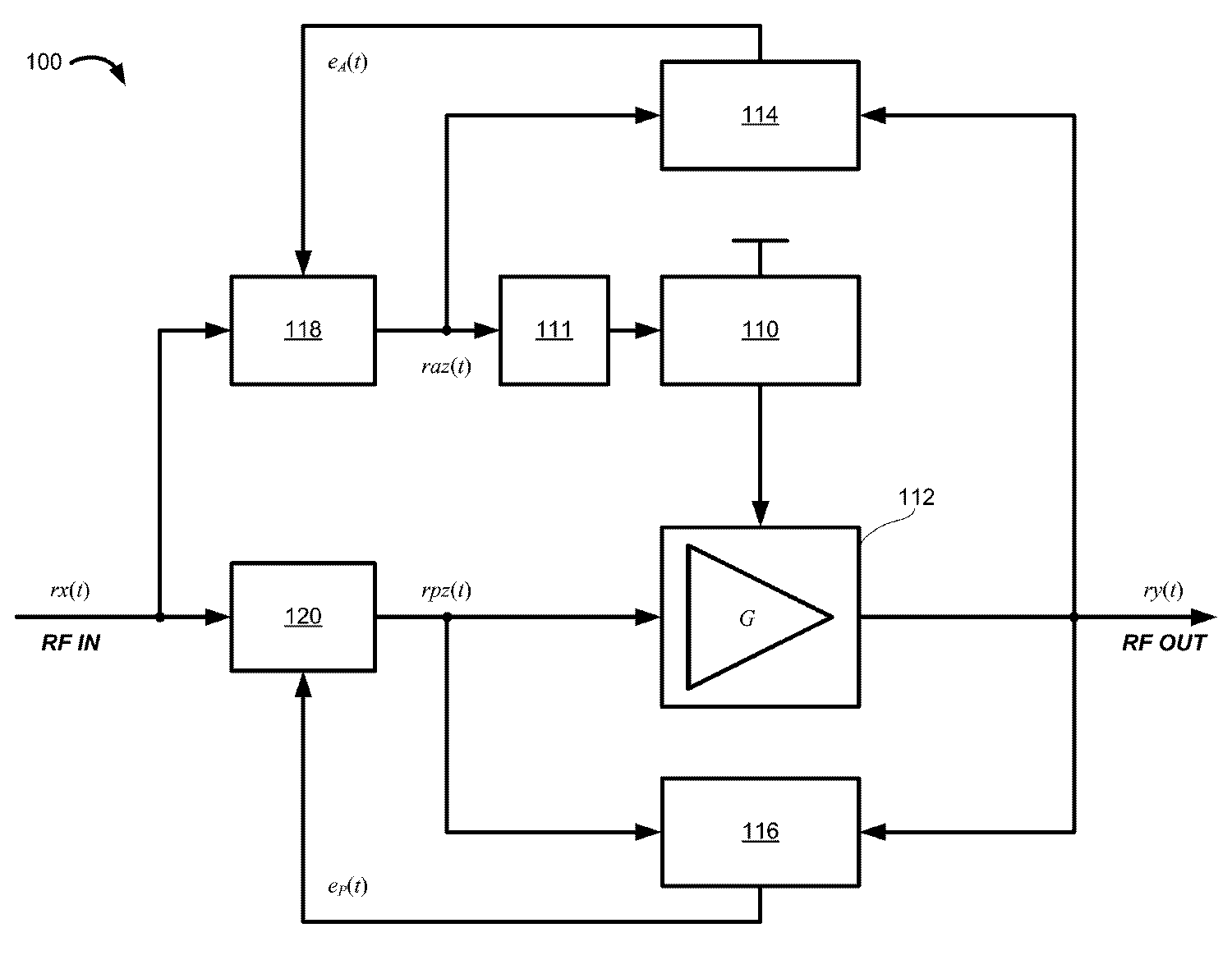
- 입력 진폭 신호 및 입력 위상 신호를 생성하는 단계- 상기 입력 진폭 신호와 상기 입력 위상 신호는 입력 신호의 직교 성분이며, 각각 제1 신호 경로 및 제2 신호 경로 상에서 생성됨;진폭 오차 신호를 이용하여 상기 제1 신호 경로를 따라 상기 입력 진폭 신호를 처리하여 전치왜곡된 진폭 신호를 생성하는 단계;위상 오차 신호를 이용하여 상기 제2 신호 경로를 따라 상기 입력 위상 신호를 처리하여 전치왜곡된 위상 신호를 생성하는 단계;상기 제1 신호 경로를 따라 상기 전치왜곡된 진폭 신호를 전력 증폭기에 제공하고, 상기 제2 신호 경로를 따라 상기 전치왜곡된 위상 신호를 상기 전력 증폭기에 제공하여, 출력 신호를 생성하는 단계;상기 전력 증폭기의 상기 출력 신호에 제1 로그 증폭기를 적용하여 로그-검출된(log-detected) 출력 신호를 획득하고, 상기 전치왜곡된 진폭 신호에 제2 로그 증폭기를 적용하여 로그-검출되고 전치왜곡된 진폭 신호를 획득하는 단계; 및상기 전력 증폭기의 출력 신호에 제1 진폭 제한기를 적용하여 진폭-제한된(amplitude-limited) 출력 신호를 획득하고, 상기 전치왜곡된 위상 신호에 제2 진폭 제한기를 적용하여 진폭-제한되고 전치왜곡된 위상 신호를 획득하는 단계를 포함하며,상기 진폭 오차 신호는 상기 로그-검출된 출력 신호의 적어도 일부와 상기 로그-검출되고 전치왜곡된 진폭 신호를 비교하여 생성되고, 상기 위상 오차 신호는 상기 진폭-제한된 출력 신호의 적어도 일부와 상기 진폭-제한되고 전치왜곡된 위상 신호를 비교하여 생성되는 것을 특징으로 하는 선형 포락선 제거 및 복원 송신기 제공 방법.
- 제1항에 있어서,상기 전치왜곡된 진폭 신호를 생성하는 단계는, 상기 입력 진폭 신호와 상기 진폭 오차 신호를 승산하는 단계를 포함하는 것을 특징으로 하는 선형 포락선 제거 및 복원 송신기 제공 방법.
- 제2항에 있어서,상기 입력 진폭 신호는 가변 이득 증폭기를 이용하여 상기 진폭 오차 신호와 승산되는 것을 특징으로 하는 선형 포락선 제거 및 복원 송신기 제공 방법.
- 제1항에 있어서,상기 입력 위상 신호는 전압 제어 가변 위상 시프터를 이용하여 상기 위상 오차 신호에 가산되는 것을 특징으로 하는 선형 포락선 제거 및 복원 송신기 제공 방법.
- 제1항에 있어서,상기 입력 진폭 신호 및 입력 위상 신호를 생성하는 단계는, 상기 제1 신호 경로 상에 입력 진폭 벡터를 생성하고, 상기 제2 신호 경로 상에 입력 위상 벡터를 생성하는 단계를 포함하는 것을 특징으로 하는 선형 포락선 제거 및 복원 송신기 제공 방법.
- 제1항에 있어서,상기 진폭 오차 신호는 상기 전력 증폭기 전달함수의 역수의 형태로 표현되는 것을 특징으로 하는 선형 포락선 제거 및 복원 송신기 제공 방법.
- 제1항에 있어서,상기 진폭 오차 신호는 상기 로그-검출되고 전치왜곡된 진폭 신호에서 상기 로그-검출된 출력 신호를 감산함으로써 생성되는 것을 특징으로 하는 선형 포락선 제거 및 복원 송신기 제공 방법.
- 제7항에 있어서,상기 로그-검출된 출력 신호는, 차동 오차 증폭기를 이용하여 상기 로그-검출되고 전치왜곡된 진폭 신호에서 감산되는 것을 특징으로 하는 선형 포락선 제거 및 복원 송신기 제공 방법.
- 제1항에 있어서,상기 위상 오차 신호는 상기 진폭-제한되고 전치왜곡된 위상 신호로 상기 진폭-제한된 출력 신호를 승산함으로써 생성되는 것을 특징으로 하는 선형 포락선 제거 및 복원 송신기 제공 방법.
- 입력 진폭 신호 및 입력 위상 신호- 상기 입력 진폭 신호와 상기 입력 위상 신호는 입력 신호의 직교 성분이며, 각각 제1 신호 경로 및 제2 신호 경로 상에 제공됨;역 진폭 오차 신호(inverse amplitude error signal)를 이용하여 상기 제1 신호 경로를 따라 상기 입력 진폭 신호를 처리하여 전치왜곡된 진폭 신호를 생성하는 제1 전치왜곡 모듈;역 위상 오차 신호(inverse phase error signal)를 이용하여 상기 제2 신호 경로를 따라 상기 입력 위상 신호를 처리하여 전치왜곡된 위상 신호를 생성하는 제2 전치왜곡 모듈;상기 제1 신호 경로를 따라 상기 전치왜곡된 진폭 신호를 입력받고 상기 제2 신호 경로를 따라 상기 전치왜곡된 위상 신호를 입력받아, 상기 전치왜곡된 진폭 신호 및 상기 전치왜곡된 위상 신호에 기반하여 출력 신호를 생성하는 전력 증폭기;상기 전력 증폭기의 상기 출력 신호로부터 로그-검출된(log-detected) 출력 신호를 구하고, 상기 전치왜곡된 진폭 신호로부터 로그-검출되고 전치왜곡된 진폭 신호를 구하는 적어도 하나의 로그 증폭기; 및상기 전력 증폭기의 출력 신호로부터 진폭-제한된(amplitude-limited) 출력 신호를 획득하고, 상기 전치왜곡된 위상 신호로부터 진폭-제한되고 전치왜곡된 위상 신호를 구하는 적어도 하나의 진폭 제한기를 포함하며,상기 진폭 오차 신호는 상기 로그-검출된 출력 신호의 적어도 일부와 상기 로그-검출되고 전치왜곡된 진폭 신호를 비교하여 생성되고, 상기 위상 오차 신호는 상기 진폭-제한된 출력 신호의 적어도 일부와 상기 진폭-제한되고 전치왜곡된 위상 신호를 비교하여 생성되는 것을 특징으로 하는 선형 포락선 제거 및 복원 송신기 시스템.
- 제10항에 있어서,상기 제1 전치왜곡 모듈은, 상기 입력 진폭 신호와 상기 진폭 오차 신호를 승산하여 입력 진폭 신호를 처리하는 것을 특징으로 하는 선형 포락선 제거 및 복원 송신기 시스템.
- 제10항에 있어서,상기 제1 전치왜곡 모듈은 상기 입력 진폭 신호와 상기 진폭 오차 신호를 승산하기 위한 가변 이득 증폭기를 포함하는 것을 특징으로 하는 선형 포락선 제거 및 복원 송신기 시스템.
- 제10항에 있어서,상기 제2 전치왜곡 모듈은 상기 입력 위상 신호와 상기 위상 오차 신호를 가산하기 위한 전압 제어 가변 위상 시프터를 포함하는 것을 특징으로 하는 선형 포락선 제거 및 복원 송신기 시스템.
- 제10항에 있어서,상기 입력 진폭 신호는 상기 제1 신호 경로 상에 입력 진폭 벡터를 포함하고, 상기 입력 위상 신호는 상기 제2 신호 경로 상에 입력 위상 벡터를 포함하는 것을 특징으로 하는 선형 포락선 제거 및 복원 송신기 시스템.
- 제10항에 있어서,상기 진폭 오차 신호는 상기 전력 증폭기 전달함수의 역수의 형태로 표현되는 것을 특징으로 하는 선형 포락선 제거 및 복원 송신기 시스템.
- 제10항에 있어서,상기 진폭 오차 신호는 상기 로그-검출되고 전치왜곡된 진폭 신호에서 상기 로그-검출된 출력 신호를 감산함으로써 생성되는 것을 특징으로 하는 선형 포락선 제거 및 복원 송신기 시스템.
- 제16항에 있어서,상기 로그-검출되고 전치왜곡된 진폭 신호에서 상기 로그-검출된 출력 신호 를 감산하기 위한 차동 오차 증폭기를 더 포함하는 것을 특징으로 하는 선형 포락선 제거 및 복원 송신기 시스템.
- 제10항에 있어서,상기 위상 오차 신호는 상기 진폭-제한되고 전치왜곡된 위상 신호로 상기 진폭-제한된 출력 신호를 승산함으로써 생성되는 것을 특징으로 하는 선형 포락선 제거 및 복원 송신기 시스템.
- 입력 진폭 신호 및 입력 위상 신호- 상기 입력 진폭 신호와 상기 입력 위상 신호는 입력 신호의 직교 성분이며, 각각 제1 신호 경로 및 제2 신호 경로 상에 제공됨;역 진폭 오차 신호(inverse amplitude error signal)를 이용하여 상기 제1 신호 경로를 따라 상기 입력 진폭 신호를 처리하여 전치왜곡된 진폭 신호를 생성하기 위한 제1 수단;역 위상 오차 신호(inverse phase error signal)를 이용하여 상기 제2 신호 경로를 따라 상기 입력 위상 신호를 처리하여 전치왜곡된 위상 신호를 생성하기 위한 제2 수단;상기 제1 신호 경로를 따라 상기 전치왜곡된 진폭 신호를 입력받고 상기 제2 신호 경로를 따라 상기 전치왜곡된 위상 신호를 입력받아, 상기 전치왜곡된 진폭 신호 및 상기 전치왜곡된 위상 신호에 기반하여 출력 신호를 생성하는 전력 증폭 기;상기 출력 신호 및 상기 전치왜곡된 진폭 신호로부터 상기 역 진폭 오차 신호를 생성하기 위한 제3 수단; 및상기 출력 신호 및 상기 전치왜곡된 위상 신호로부터 상기 역 위상 오차 신호를 생성하기 위한 제4 수단을 포함하는 선형 포락선 제거 및 복원 송신기 제공 시스템.
- 제19항에 있어서,상기 제3 수단은, 상기 전력 증폭기의 상기 출력 신호로부터 로그-검출된(log-detected) 출력 신호를 구하고, 상기 전치왜곡된 진폭 신호로부터 로그-검출되고 전치왜곡된 진폭 신호를 구하는 적어도 하나의 로그 증폭기를 포함하며,상기 제4 수단은, 상기 전력 증폭기의 출력 신호로부터 진폭-제한된(amplitude-limited) 출력 신호를 구하고, 상기 전치왜곡된 위상 신호로부터 진폭-제한되고 전치왜곡된 위상 신호를 구하는 적어도 하나의 진폭 제한기를 포함하는 것을 특징으로 하는 선형 포락선 제거 및 복원 송신기 제공 시스템.
Applications Claiming Priority (4)
| Application Number | Priority Date | Filing Date | Title |
|---|---|---|---|
| US80387106P | 2006-06-04 | 2006-06-04 | |
| US60/803,871 | 2006-06-04 | ||
| US11/754,119 US7518445B2 (en) | 2006-06-04 | 2007-05-25 | Systems, methods, and apparatuses for linear envelope elimination and restoration transmitters |
| US11/754,119 | 2007-05-25 |
Publications (2)
| Publication Number | Publication Date |
|---|---|
| KR20070116205A KR20070116205A (ko) | 2007-12-07 |
| KR100867548B1 true KR100867548B1 (ko) | 2008-11-06 |
Family
ID=38289782
Family Applications (1)
| Application Number | Title | Priority Date | Filing Date |
|---|---|---|---|
| KR1020070054711A Expired - Fee Related KR100867548B1 (ko) | 2006-06-04 | 2007-06-04 | 선형 포락선 제거 및 복원 송신기 시스템, 방법 및 장치 |
Country Status (5)
| Country | Link |
|---|---|
| US (2) | US7518445B2 (ko) |
| KR (1) | KR100867548B1 (ko) |
| DE (1) | DE102007026022A1 (ko) |
| FR (1) | FR2924539A1 (ko) |
| GB (1) | GB2438749B8 (ko) |
Families Citing this family (37)
| Publication number | Priority date | Publication date | Assignee | Title |
|---|---|---|---|---|
| GB2389253B (en) * | 2002-05-31 | 2005-09-21 | Hitachi Ltd | Transmitter and semiconductor integrated circuit for communication |
| US7558542B2 (en) * | 2006-06-09 | 2009-07-07 | Mediatek Inc. | System and method for providing a transmitter for polar modulation and power amplifier linearization |
| US7729670B2 (en) * | 2006-09-29 | 2010-06-01 | Broadcom Corporation | Method and system for minimizing power consumption in a communication system |
| US20090042520A1 (en) * | 2007-08-07 | 2009-02-12 | Harris Corporation | Envelope tracking RF amplifier |
| US20090139972A1 (en) * | 2007-10-23 | 2009-06-04 | Psion Teklogix Inc. | Docking connector |
| CN101217522A (zh) * | 2007-12-27 | 2008-07-09 | 华为技术有限公司 | 确定开环预失真参数的方法和装置、发信机和发信方法 |
| DE112009001227T5 (de) * | 2008-05-21 | 2011-04-07 | Silicon Laboratories, Inc., Austin | Prädiktive Rückkopplungskompensation für PWM-Schaltverstärker |
| EP2144365A1 (en) * | 2008-07-11 | 2010-01-13 | Alcatel Lucent | Device for amplifying signals with an envelope tracking technique or an envelope extraction and restoration technique controlled by a switched modulation |
| ATE534188T1 (de) * | 2009-09-30 | 2011-12-15 | Alcatel Lucent | Hüllkurvennachführungsverstärkungsanordnung |
| JP5036839B2 (ja) * | 2010-03-24 | 2012-09-26 | 株式会社東芝 | 電力増幅器及び半導体集積回路 |
| EP2728743A1 (en) * | 2010-12-22 | 2014-05-07 | Sumitomo Electric Industries, Ltd. | Amplifier circuit and wireless communication equipment |
| GB2498391B (en) * | 2012-01-16 | 2018-11-21 | Snaptrack Inc | Pre-distortion in RF path in combination with shaping table in envelope path for envelope tracking amplifier |
| JPWO2013145748A1 (ja) * | 2012-03-30 | 2015-12-10 | 日本電気株式会社 | 増幅器および増幅方法 |
| WO2014050218A1 (ja) * | 2012-09-25 | 2014-04-03 | 株式会社日立国際電気 | 歪み補償回路および歪み補償回路と高周波電力増幅器を用いた送信装置 |
| US8841968B2 (en) * | 2012-09-26 | 2014-09-23 | Broadcom Corporation | Class-AB radio frequency amplifier for envelope detector |
| GB201309235D0 (en) * | 2013-05-22 | 2013-07-03 | Nujira Ltd | Transfer function regulation |
| US11140018B2 (en) * | 2014-01-07 | 2021-10-05 | Quantumsine Acquisitions Inc. | Method and apparatus for intra-symbol multi-dimensional modulation |
| US10382246B2 (en) * | 2014-01-07 | 2019-08-13 | Quantumsine Acquisitions Inc. | Combined amplitude-time and phase modulation |
| WO2016187055A1 (en) * | 2015-05-15 | 2016-11-24 | Crocus Technology Inc. | Mram-based pre-distortion linearization and amplification circuits |
| US9748901B2 (en) | 2015-06-16 | 2017-08-29 | Avago Technologies General Ip (Singapore) Pte. Ltd. | Power amplifying apparatus |
| US11025458B2 (en) * | 2019-02-07 | 2021-06-01 | Qorvo Us, Inc. | Adaptive frequency equalizer for wide modulation bandwidth envelope tracking |
| US11671064B2 (en) | 2020-01-07 | 2023-06-06 | Qorvo Us, Inc. | Equalizer for envelope power supply circuitry |
| US11677365B2 (en) | 2020-01-08 | 2023-06-13 | Qorvo Us, Inc. | Envelope tracking power management apparatus incorporating multiple power amplifiers |
| US11716057B2 (en) | 2020-01-28 | 2023-08-01 | Qorvo Us, Inc. | Envelope tracking circuitry |
| US11728774B2 (en) | 2020-02-26 | 2023-08-15 | Qorvo Us, Inc. | Average power tracking power management integrated circuit |
| US11545945B2 (en) * | 2020-03-04 | 2023-01-03 | Qorvo Us, Inc. | Apparatus and method for calibrating an envelope tracking lookup table |
| US11626844B2 (en) | 2020-03-09 | 2023-04-11 | Qorvo Us, Inc. | Envelope tracking radio frequency front-end circuit |
| US11482975B2 (en) | 2020-06-05 | 2022-10-25 | Skyworks Solutions, Inc. | Power amplifiers with adaptive bias for envelope tracking applications |
| US11855595B2 (en) * | 2020-06-05 | 2023-12-26 | Skyworks Solutions, Inc. | Composite cascode power amplifiers for envelope tracking applications |
| US11909385B2 (en) | 2020-10-19 | 2024-02-20 | Qorvo Us, Inc. | Fast-switching power management circuit and related apparatus |
| WO2022119626A1 (en) | 2020-12-04 | 2022-06-09 | Qorvo Us, Inc. | Power management integrated circuit |
| US12212285B2 (en) | 2020-12-22 | 2025-01-28 | Qorvo Us, Inc. | Power management apparatus operable with multiple configurations |
| US12267046B2 (en) | 2021-02-15 | 2025-04-01 | Qorvo Us, Inc. | Power amplifier system |
| US12068720B2 (en) | 2021-02-26 | 2024-08-20 | Qorvo Us, Inc. | Barely Doherty dual envelope tracking (BD2E) circuit |
| US12212286B2 (en) | 2021-03-05 | 2025-01-28 | Qorvo Us, Inc. | Complementary envelope detector |
| US12126305B2 (en) | 2021-05-27 | 2024-10-22 | Qorvo Us, Inc. | Radio frequency (RF) equalizer in an envelope tracking (ET) circuit |
| US12063018B2 (en) | 2021-06-10 | 2024-08-13 | Qorvo Us, Inc. | Envelope tracking integrated circuit operable with multiple types of power amplifiers |
Citations (3)
| Publication number | Priority date | Publication date | Assignee | Title |
|---|---|---|---|---|
| KR20010064260A (ko) * | 1999-12-27 | 2001-07-09 | 오길록 | 비선형 왜곡 보상을 위한 적응 전치 왜곡기 |
| KR20040016366A (ko) * | 2002-08-15 | 2004-02-21 | 한국전자통신연구원 | 구간별 차등 다항식을 이용한 사전 왜곡 방법 및 그를이용한 고전력 증폭기의 사전 왜곡 장치 |
| JP2005269440A (ja) | 2004-03-19 | 2005-09-29 | Matsushita Electric Ind Co Ltd | ポーラ変調送信装置及びポーラ変調方法 |
Family Cites Families (26)
| Publication number | Priority date | Publication date | Assignee | Title |
|---|---|---|---|---|
| US5140703A (en) * | 1988-10-14 | 1992-08-18 | Payne Christopher P | Modulation distortion analyzer |
| US5420536A (en) * | 1993-03-16 | 1995-05-30 | Victoria University Of Technology | Linearized power amplifier |
| US6801516B1 (en) | 1995-06-30 | 2004-10-05 | Interdigital Technology Corporation | Spread-spectrum system for assigning information signals having different data rates |
| ZA965340B (en) | 1995-06-30 | 1997-01-27 | Interdigital Tech Corp | Code division multiple access (cdma) communication system |
| US5742201A (en) | 1996-01-30 | 1998-04-21 | Spectrian | Polar envelope correction mechanism for enhancing linearity of RF/microwave power amplifier |
| US5923712A (en) | 1997-05-05 | 1999-07-13 | Glenayre Electronics, Inc. | Method and apparatus for linear transmission by direct inverse modeling |
| US6295442B1 (en) * | 1998-12-07 | 2001-09-25 | Ericsson Inc. | Amplitude modulation to phase modulation cancellation method in an RF amplifier |
| US6236267B1 (en) * | 1998-12-29 | 2001-05-22 | International Business Machines Corporation | Linearization for power amplifiers using feed-forward and feedback control |
| JP2000209294A (ja) | 1998-12-30 | 2000-07-28 | Texas Instr Inc <Ti> | 振幅位相変調信号を供給するための回路と方法 |
| US6449465B1 (en) * | 1999-12-20 | 2002-09-10 | Motorola, Inc. | Method and apparatus for linear amplification of a radio frequency signal |
| CA2329100A1 (en) * | 1999-12-21 | 2001-06-21 | Nortel Networks Limited | Phase and amplitude detector and method of determining errors |
| WO2002033844A2 (en) | 2000-10-18 | 2002-04-25 | Telefonaktiebolaget Lm Ericsson (Publ) | Communications systems |
| GB2369941A (en) | 2000-12-09 | 2002-06-12 | Roke Manor Research | A polar loop amplifier arrangement with variable gain in a feedback loop |
| GB2376584B (en) | 2001-06-15 | 2005-02-16 | Wireless Systems Int Ltd | Signal correction techniques |
| US7409004B2 (en) | 2001-06-19 | 2008-08-05 | Matsushita Electric Industrial Co., Ltd. | Hybrid polar modulator differential phase Cartesian feedback correction circuit for power amplifier linearization |
| GB2380880B (en) | 2001-10-10 | 2004-02-11 | Zarlink Semiconductor Ltd | A polar loop transmitter |
| SE520466C2 (sv) | 2001-11-12 | 2003-07-15 | Ericsson Telefon Ab L M | Metod och anordning vid en digital linjäriseringskoppling |
| JPWO2003073605A1 (ja) | 2002-02-28 | 2005-06-23 | 富士通株式会社 | 高周波増幅回路 |
| US7024620B2 (en) * | 2002-03-08 | 2006-04-04 | Hewlett-Packard Development Company, L.P. | Point-of-need document production system and method |
| US6794938B2 (en) | 2002-03-19 | 2004-09-21 | The University Of North Carolina At Charlotte | Method and apparatus for cancellation of third order intermodulation distortion and other nonlinearities |
| DE10257435B3 (de) | 2002-11-14 | 2004-09-09 | Fraunhofer-Gesellschaft zur Förderung der angewandten Forschung e.V. | Sendestufe |
| DE50305069D1 (de) | 2002-11-14 | 2006-10-26 | Fraunhofer Ges Forschung | Sendestufe mit phasen und amplitudenregelschleife |
| JP3844352B2 (ja) | 2003-08-07 | 2006-11-08 | 松下電器産業株式会社 | 送信装置 |
| US7330073B2 (en) | 2004-10-06 | 2008-02-12 | Telefonaktiebolaget L M Ericsson (Publ) | Arbitrary waveform predistortion table generation |
| DE102005006162B3 (de) | 2005-02-10 | 2006-08-17 | Infineon Technologies Ag | Sende-/Empfangseinrichtung mit einem eine einstellbare Vorverzerrung aufweisenden Polar-Modulator |
| US7532676B2 (en) | 2005-10-20 | 2009-05-12 | Trellis Phase Communications, Lp | Single sideband and quadrature multiplexed continuous phase modulation |
-
2007
- 2007-05-25 US US11/754,119 patent/US7518445B2/en active Active
- 2007-06-04 GB GB0710602A patent/GB2438749B8/en not_active Expired - Fee Related
- 2007-06-04 DE DE102007026022A patent/DE102007026022A1/de not_active Withdrawn
- 2007-06-04 KR KR1020070054711A patent/KR100867548B1/ko not_active Expired - Fee Related
- 2007-06-04 FR FR0703974A patent/FR2924539A1/fr not_active Withdrawn
-
2009
- 2009-03-18 US US12/406,183 patent/US7888997B2/en not_active Expired - Fee Related
Patent Citations (3)
| Publication number | Priority date | Publication date | Assignee | Title |
|---|---|---|---|---|
| KR20010064260A (ko) * | 1999-12-27 | 2001-07-09 | 오길록 | 비선형 왜곡 보상을 위한 적응 전치 왜곡기 |
| KR20040016366A (ko) * | 2002-08-15 | 2004-02-21 | 한국전자통신연구원 | 구간별 차등 다항식을 이용한 사전 왜곡 방법 및 그를이용한 고전력 증폭기의 사전 왜곡 장치 |
| JP2005269440A (ja) | 2004-03-19 | 2005-09-29 | Matsushita Electric Ind Co Ltd | ポーラ変調送信装置及びポーラ変調方法 |
Also Published As
| Publication number | Publication date |
|---|---|
| KR20070116205A (ko) | 2007-12-07 |
| US20070290748A1 (en) | 2007-12-20 |
| US7518445B2 (en) | 2009-04-14 |
| FR2924539A1 (fr) | 2009-06-05 |
| GB2438749B8 (en) | 2011-07-13 |
| GB2438749A (en) | 2007-12-05 |
| DE102007026022A1 (de) | 2008-01-24 |
| GB2438749A8 (en) | 2008-11-26 |
| GB0710602D0 (en) | 2007-07-11 |
| GB2438749B (en) | 2011-02-16 |
| US20090174473A1 (en) | 2009-07-09 |
| US7888997B2 (en) | 2011-02-15 |
Similar Documents
| Publication | Publication Date | Title |
|---|---|---|
| KR100867548B1 (ko) | 선형 포락선 제거 및 복원 송신기 시스템, 방법 및 장치 | |
| CN101090380B (zh) | 用于线性包络消除与恢复发射机的系统以及方法 | |
| KR100872277B1 (ko) | 선형 폴라 송신기 시스템, 방법 및 장치 | |
| KR100862491B1 (ko) | 다중-경로 직교 순환 전치왜곡 시스템, 방법 및 장치 | |
| US11394350B2 (en) | Method and system for aligning signals widely spaced in frequency for wideband digital predistortion in wireless communication systems | |
| Zhang et al. | Design of linear RF outphasing power amplifiers | |
| US9768739B2 (en) | Digital hybrid mode power amplifier system | |
| US20080074186A1 (en) | An Arrangement And A Method Relating To Signal Predistortion | |
| Zavosh et al. | Digital predistortion techniques for RF power amplifiers with CDMA applications | |
| US7274255B2 (en) | Efficient generation of radio frequency currents | |
| Rawat et al. | Compensating I–Q imperfections in hybrid RF/digital predistortion with an adapted lookup table implemented in an FPGA | |
| Pham | Contribution to dimensionality reduction of digital predistorter behavioral models for RF power amplifier linearization | |
| Zozaya et al. | Passivity theory applied to the design of power-amplifier linearizers | |
| O'Droma et al. | Developments in predistortion and feedforward adaptive power amplifier linearisers | |
| El-Khatib et al. | Modulation schemes effect on RF power amplifier nonlinearity and RFPA linearization techniques | |
| CN100525079C (zh) | 模拟预失真线性化方法及实现所述方法的装置 | |
| Nasr et al. | On the critical issues of DSP/FPGA mixed digital predistorter implementation | |
| KR101415541B1 (ko) | Rf 왜곡신호 측정 장치, 이를 포함하는 무선 전력 증폭 장치 및 rf 왜곡신호 측정 방법 | |
| Ohmori et al. | An adaptive predistortion method based on orthogonal polynomial expansion for nonlinear distortion compensation | |
| Woo et al. | Wideband predistortion linearization system for RF power amplifiers using an envelope modulation technique | |
| Boiko et al. | Optimization of Cartesian Feedback Loops for Wideband SDR Transmitters in 5G Mobile Networks | |
| Wada et al. | Advances in Digital Front-End and Software RF Processing: Part I | |
| Gandla | Digital Techniques for Compensation of Radio Frequency Impairments in Mobile Communication Terminals | |
| Ibrahim | Feedforward Linearization of a Power Amplifier for Wireless Communication Systems | |
| Hamdane et al. | Linearization of class B amplifier and application to outphasing systems |
Legal Events
| Date | Code | Title | Description |
|---|---|---|---|
| A201 | Request for examination | ||
| PA0109 | Patent application |
Patent event code: PA01091R01D Comment text: Patent Application Patent event date: 20070604 |
|
| PA0201 | Request for examination | ||
| PG1501 | Laying open of application | ||
| E902 | Notification of reason for refusal | ||
| PE0902 | Notice of grounds for rejection |
Comment text: Notification of reason for refusal Patent event date: 20080429 Patent event code: PE09021S01D |
|
| E701 | Decision to grant or registration of patent right | ||
| PE0701 | Decision of registration |
Patent event code: PE07011S01D Comment text: Decision to Grant Registration Patent event date: 20081029 |
|
| GRNT | Written decision to grant | ||
| PR0701 | Registration of establishment |
Comment text: Registration of Establishment Patent event date: 20081031 Patent event code: PR07011E01D |
|
| PR1002 | Payment of registration fee |
Payment date: 20081031 End annual number: 3 Start annual number: 1 |
|
| PG1601 | Publication of registration | ||
| FPAY | Annual fee payment |
Payment date: 20111010 Year of fee payment: 4 |
|
| PR1001 | Payment of annual fee |
Payment date: 20111010 Start annual number: 4 End annual number: 4 |
|
| FPAY | Annual fee payment |
Payment date: 20121002 Year of fee payment: 5 |
|
| PR1001 | Payment of annual fee |
Payment date: 20121002 Start annual number: 5 End annual number: 5 |
|
| LAPS | Lapse due to unpaid annual fee | ||
| PC1903 | Unpaid annual fee |