JP7707079B2 - カメラモジュールおよびカメラモジュールの製造方法 - Google Patents
カメラモジュールおよびカメラモジュールの製造方法 Download PDFInfo
- Publication number
- JP7707079B2 JP7707079B2 JP2021565544A JP2021565544A JP7707079B2 JP 7707079 B2 JP7707079 B2 JP 7707079B2 JP 2021565544 A JP2021565544 A JP 2021565544A JP 2021565544 A JP2021565544 A JP 2021565544A JP 7707079 B2 JP7707079 B2 JP 7707079B2
- Authority
- JP
- Japan
- Prior art keywords
- component
- mounting board
- spacer
- component mounting
- camera module
- Prior art date
- Legal status (The legal status is an assumption and is not a legal conclusion. Google has not performed a legal analysis and makes no representation as to the accuracy of the status listed.)
- Active
Links
Images


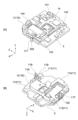


Classifications
-
- G—PHYSICS
- G03—PHOTOGRAPHY; CINEMATOGRAPHY; ANALOGOUS TECHNIQUES USING WAVES OTHER THAN OPTICAL WAVES; ELECTROGRAPHY; HOLOGRAPHY
- G03B—APPARATUS OR ARRANGEMENTS FOR TAKING PHOTOGRAPHS OR FOR PROJECTING OR VIEWING THEM; APPARATUS OR ARRANGEMENTS EMPLOYING ANALOGOUS TECHNIQUES USING WAVES OTHER THAN OPTICAL WAVES; ACCESSORIES THEREFOR
- G03B17/00—Details of cameras or camera bodies; Accessories therefor
- G03B17/02—Bodies
-
- G—PHYSICS
- G03—PHOTOGRAPHY; CINEMATOGRAPHY; ANALOGOUS TECHNIQUES USING WAVES OTHER THAN OPTICAL WAVES; ELECTROGRAPHY; HOLOGRAPHY
- G03B—APPARATUS OR ARRANGEMENTS FOR TAKING PHOTOGRAPHS OR FOR PROJECTING OR VIEWING THEM; APPARATUS OR ARRANGEMENTS EMPLOYING ANALOGOUS TECHNIQUES USING WAVES OTHER THAN OPTICAL WAVES; ACCESSORIES THEREFOR
- G03B30/00—Camera modules comprising integrated lens units and imaging units, specially adapted for being embedded in other devices, e.g. mobile phones or vehicles
-
- H—ELECTRICITY
- H01—ELECTRIC ELEMENTS
- H01R—ELECTRICALLY-CONDUCTIVE CONNECTIONS; STRUCTURAL ASSOCIATIONS OF A PLURALITY OF MUTUALLY-INSULATED ELECTRICAL CONNECTING ELEMENTS; COUPLING DEVICES; CURRENT COLLECTORS
- H01R12/00—Structural associations of a plurality of mutually-insulated electrical connecting elements, specially adapted for printed circuits, e.g. printed circuit boards [PCB], flat or ribbon cables, or like generally planar structures, e.g. terminal strips, terminal blocks; Coupling devices specially adapted for printed circuits, flat or ribbon cables, or like generally planar structures; Terminals specially adapted for contact with, or insertion into, printed circuits, flat or ribbon cables, or like generally planar structures
- H01R12/70—Coupling devices
- H01R12/71—Coupling devices for rigid printing circuits or like structures
- H01R12/712—Coupling devices for rigid printing circuits or like structures co-operating with the surface of the printed circuit or with a coupling device exclusively provided on the surface of the printed circuit
- H01R12/716—Coupling device provided on the PCB
-
- H—ELECTRICITY
- H04—ELECTRIC COMMUNICATION TECHNIQUE
- H04N—PICTORIAL COMMUNICATION, e.g. TELEVISION
- H04N23/00—Cameras or camera modules comprising electronic image sensors; Control thereof
- H04N23/50—Constructional details
- H04N23/51—Housings
-
- H—ELECTRICITY
- H04—ELECTRIC COMMUNICATION TECHNIQUE
- H04N—PICTORIAL COMMUNICATION, e.g. TELEVISION
- H04N23/00—Cameras or camera modules comprising electronic image sensors; Control thereof
- H04N23/50—Constructional details
- H04N23/52—Elements optimising image sensor operation, e.g. for electromagnetic interference [EMI] protection or temperature control by heat transfer or cooling elements
-
- H—ELECTRICITY
- H04—ELECTRIC COMMUNICATION TECHNIQUE
- H04N—PICTORIAL COMMUNICATION, e.g. TELEVISION
- H04N23/00—Cameras or camera modules comprising electronic image sensors; Control thereof
- H04N23/50—Constructional details
- H04N23/54—Mounting of pick-up tubes, electronic image sensors, deviation or focusing coils
-
- H—ELECTRICITY
- H04—ELECTRIC COMMUNICATION TECHNIQUE
- H04N—PICTORIAL COMMUNICATION, e.g. TELEVISION
- H04N23/00—Cameras or camera modules comprising electronic image sensors; Control thereof
- H04N23/57—Mechanical or electrical details of cameras or camera modules specially adapted for being embedded in other devices
-
- H—ELECTRICITY
- H05—ELECTRIC TECHNIQUES NOT OTHERWISE PROVIDED FOR
- H05K—PRINTED CIRCUITS; CASINGS OR CONSTRUCTIONAL DETAILS OF ELECTRIC APPARATUS; MANUFACTURE OF ASSEMBLAGES OF ELECTRICAL COMPONENTS
- H05K1/00—Printed circuits
- H05K1/02—Details
- H05K1/0201—Thermal arrangements, e.g. for cooling, heating or preventing overheating
- H05K1/0203—Cooling of mounted components
- H05K1/0209—External configuration of printed circuit board adapted for heat dissipation, e.g. lay-out of conductors, coatings
-
- H—ELECTRICITY
- H05—ELECTRIC TECHNIQUES NOT OTHERWISE PROVIDED FOR
- H05K—PRINTED CIRCUITS; CASINGS OR CONSTRUCTIONAL DETAILS OF ELECTRIC APPARATUS; MANUFACTURE OF ASSEMBLAGES OF ELECTRICAL COMPONENTS
- H05K1/00—Printed circuits
- H05K1/02—Details
- H05K1/14—Structural association of two or more printed circuits
- H05K1/144—Stacked arrangements of planar printed circuit boards
-
- H—ELECTRICITY
- H05—ELECTRIC TECHNIQUES NOT OTHERWISE PROVIDED FOR
- H05K—PRINTED CIRCUITS; CASINGS OR CONSTRUCTIONAL DETAILS OF ELECTRIC APPARATUS; MANUFACTURE OF ASSEMBLAGES OF ELECTRICAL COMPONENTS
- H05K1/00—Printed circuits
- H05K1/18—Printed circuits structurally associated with non-printed electric components
- H05K1/181—Printed circuits structurally associated with non-printed electric components associated with surface mounted components
-
- H—ELECTRICITY
- H05—ELECTRIC TECHNIQUES NOT OTHERWISE PROVIDED FOR
- H05K—PRINTED CIRCUITS; CASINGS OR CONSTRUCTIONAL DETAILS OF ELECTRIC APPARATUS; MANUFACTURE OF ASSEMBLAGES OF ELECTRICAL COMPONENTS
- H05K13/00—Apparatus or processes specially adapted for manufacturing or adjusting assemblages of electric components
- H05K13/0015—Orientation; Alignment; Positioning
-
- H—ELECTRICITY
- H05—ELECTRIC TECHNIQUES NOT OTHERWISE PROVIDED FOR
- H05K—PRINTED CIRCUITS; CASINGS OR CONSTRUCTIONAL DETAILS OF ELECTRIC APPARATUS; MANUFACTURE OF ASSEMBLAGES OF ELECTRICAL COMPONENTS
- H05K3/00—Apparatus or processes for manufacturing printed circuits
- H05K3/36—Assembling printed circuits with other printed circuits
- H05K3/368—Assembling printed circuits with other printed circuits parallel to each other
-
- G—PHYSICS
- G03—PHOTOGRAPHY; CINEMATOGRAPHY; ANALOGOUS TECHNIQUES USING WAVES OTHER THAN OPTICAL WAVES; ELECTROGRAPHY; HOLOGRAPHY
- G03B—APPARATUS OR ARRANGEMENTS FOR TAKING PHOTOGRAPHS OR FOR PROJECTING OR VIEWING THEM; APPARATUS OR ARRANGEMENTS EMPLOYING ANALOGOUS TECHNIQUES USING WAVES OTHER THAN OPTICAL WAVES; ACCESSORIES THEREFOR
- G03B2217/00—Details of cameras or camera bodies; Accessories therefor
- G03B2217/002—Details of arrangement of components in or on camera body
-
- H—ELECTRICITY
- H01—ELECTRIC ELEMENTS
- H01R—ELECTRICALLY-CONDUCTIVE CONNECTIONS; STRUCTURAL ASSOCIATIONS OF A PLURALITY OF MUTUALLY-INSULATED ELECTRICAL CONNECTING ELEMENTS; COUPLING DEVICES; CURRENT COLLECTORS
- H01R2201/00—Connectors or connections adapted for particular applications
- H01R2201/18—Connectors or connections adapted for particular applications for television
-
- H—ELECTRICITY
- H05—ELECTRIC TECHNIQUES NOT OTHERWISE PROVIDED FOR
- H05K—PRINTED CIRCUITS; CASINGS OR CONSTRUCTIONAL DETAILS OF ELECTRIC APPARATUS; MANUFACTURE OF ASSEMBLAGES OF ELECTRICAL COMPONENTS
- H05K1/00—Printed circuits
- H05K1/02—Details
- H05K1/14—Structural association of two or more printed circuits
- H05K1/145—Arrangements wherein electric components are disposed between and simultaneously connected to two planar printed circuit boards, e.g. Cordwood modules
-
- H—ELECTRICITY
- H05—ELECTRIC TECHNIQUES NOT OTHERWISE PROVIDED FOR
- H05K—PRINTED CIRCUITS; CASINGS OR CONSTRUCTIONAL DETAILS OF ELECTRIC APPARATUS; MANUFACTURE OF ASSEMBLAGES OF ELECTRICAL COMPONENTS
- H05K2201/00—Indexing scheme relating to printed circuits covered by H05K1/00
- H05K2201/04—Assemblies of printed circuits
- H05K2201/042—Stacked spaced PCBs; Planar parts of folded flexible circuits having mounted components in between or spaced from each other
-
- H—ELECTRICITY
- H05—ELECTRIC TECHNIQUES NOT OTHERWISE PROVIDED FOR
- H05K—PRINTED CIRCUITS; CASINGS OR CONSTRUCTIONAL DETAILS OF ELECTRIC APPARATUS; MANUFACTURE OF ASSEMBLAGES OF ELECTRICAL COMPONENTS
- H05K2201/00—Indexing scheme relating to printed circuits covered by H05K1/00
- H05K2201/10—Details of components or other objects attached to or integrated in a printed circuit board
- H05K2201/10007—Types of components
- H05K2201/10121—Optical component, e.g. opto-electronic component
-
- H—ELECTRICITY
- H05—ELECTRIC TECHNIQUES NOT OTHERWISE PROVIDED FOR
- H05K—PRINTED CIRCUITS; CASINGS OR CONSTRUCTIONAL DETAILS OF ELECTRIC APPARATUS; MANUFACTURE OF ASSEMBLAGES OF ELECTRICAL COMPONENTS
- H05K2201/00—Indexing scheme relating to printed circuits covered by H05K1/00
- H05K2201/10—Details of components or other objects attached to or integrated in a printed circuit board
- H05K2201/10431—Details of mounted components
- H05K2201/10568—Integral adaptations of a component or an auxiliary PCB for mounting, e.g. integral spacer element
-
- H—ELECTRICITY
- H05—ELECTRIC TECHNIQUES NOT OTHERWISE PROVIDED FOR
- H05K—PRINTED CIRCUITS; CASINGS OR CONSTRUCTIONAL DETAILS OF ELECTRIC APPARATUS; MANUFACTURE OF ASSEMBLAGES OF ELECTRICAL COMPONENTS
- H05K2201/00—Indexing scheme relating to printed circuits covered by H05K1/00
- H05K2201/10—Details of components or other objects attached to or integrated in a printed circuit board
- H05K2201/10431—Details of mounted components
- H05K2201/1059—Connections made by press-fit insertion
-
- H—ELECTRICITY
- H05—ELECTRIC TECHNIQUES NOT OTHERWISE PROVIDED FOR
- H05K—PRINTED CIRCUITS; CASINGS OR CONSTRUCTIONAL DETAILS OF ELECTRIC APPARATUS; MANUFACTURE OF ASSEMBLAGES OF ELECTRICAL COMPONENTS
- H05K2201/00—Indexing scheme relating to printed circuits covered by H05K1/00
- H05K2201/20—Details of printed circuits not provided for in H05K2201/01 - H05K2201/10
- H05K2201/2036—Permanent spacer or stand-off in a printed circuit or printed circuit assembly
Landscapes
- Engineering & Computer Science (AREA)
- Multimedia (AREA)
- Signal Processing (AREA)
- Microelectronics & Electronic Packaging (AREA)
- Physics & Mathematics (AREA)
- General Physics & Mathematics (AREA)
- Manufacturing & Machinery (AREA)
- Electromagnetism (AREA)
- Camera Bodies And Camera Details Or Accessories (AREA)
- Studio Devices (AREA)
Applications Claiming Priority (3)
| Application Number | Priority Date | Filing Date | Title |
|---|---|---|---|
| JP2019230753 | 2019-12-20 | ||
| JP2019230753 | 2019-12-20 | ||
| PCT/JP2020/046217 WO2021125074A1 (ja) | 2019-12-20 | 2020-12-11 | カメラモジュール、スペーサ部品およびカメラモジュールの製造方法 |
Publications (2)
| Publication Number | Publication Date |
|---|---|
| JPWO2021125074A1 JPWO2021125074A1 (de) | 2021-06-24 |
| JP7707079B2 true JP7707079B2 (ja) | 2025-07-14 |
Family
ID=76478759
Family Applications (1)
| Application Number | Title | Priority Date | Filing Date |
|---|---|---|---|
| JP2021565544A Active JP7707079B2 (ja) | 2019-12-20 | 2020-12-11 | カメラモジュールおよびカメラモジュールの製造方法 |
Country Status (6)
| Country | Link |
|---|---|
| US (1) | US11930258B2 (de) |
| EP (1) | EP4080263B1 (de) |
| JP (1) | JP7707079B2 (de) |
| KR (1) | KR102896429B1 (de) |
| CN (1) | CN114787680B (de) |
| WO (1) | WO2021125074A1 (de) |
Families Citing this family (6)
| Publication number | Priority date | Publication date | Assignee | Title |
|---|---|---|---|---|
| JP6780689B2 (ja) * | 2018-11-21 | 2020-11-04 | I−Pex株式会社 | 電気コネクタ及びコネクタ装置 |
| JPWO2023135720A1 (de) * | 2022-01-14 | 2023-07-20 | ||
| WO2024004821A1 (ja) | 2022-06-29 | 2024-01-04 | パナソニックIpマネジメント株式会社 | 車載用カメラ |
| EP4357848B1 (de) * | 2022-10-21 | 2026-01-07 | Aptiv Technologies AG | Kamera und verfahren zur herstellung einer kamera |
| JP2025018344A (ja) * | 2023-07-26 | 2025-02-06 | パナソニックオートモーティブシステムズ株式会社 | 車載用カメラ |
| US12610114B2 (en) * | 2023-08-07 | 2026-04-21 | Panasonic Automotive Systems Co., Ltd. | Vehicular camera |
Citations (5)
| Publication number | Priority date | Publication date | Assignee | Title |
|---|---|---|---|---|
| JP2000241864A (ja) | 1999-02-24 | 2000-09-08 | Canon Inc | 光学センサー取り付け装置およびカメラ |
| JP2003348403A (ja) | 2002-05-27 | 2003-12-05 | Olympus Optical Co Ltd | カメラ及びこれに用いる撮像素子ユニット |
| JP2014153690A (ja) | 2013-02-14 | 2014-08-25 | Alps Electric Co Ltd | レンズ駆動装置 |
| CN109845239A (zh) | 2016-10-18 | 2019-06-04 | Lg伊诺特有限公司 | 相机模块 |
| JP2019530898A (ja) | 2016-09-27 | 2019-10-24 | エスゼット ディージェイアイ テクノロジー カンパニー リミテッドSz Dji Technology Co.,Ltd | カメラおよび撮影アセンブリ |
Family Cites Families (20)
| Publication number | Priority date | Publication date | Assignee | Title |
|---|---|---|---|---|
| US7324148B2 (en) | 2002-04-26 | 2008-01-29 | Olympus Optical Co., Ltd. | Camera and image pickup device unit used therefor having a sealing structure between a dust proofing member and an image pick up device |
| JP4012428B2 (ja) * | 2002-04-30 | 2007-11-21 | 富士フイルム株式会社 | 撮像素子ユニット |
| CA2584720A1 (en) * | 2004-10-26 | 2006-05-04 | Richco Inc. | Spring loaded spacer |
| WO2008133943A1 (en) * | 2007-04-24 | 2008-11-06 | Flextronics Ap Llc | Small form factor modules using wafer level optics with bottom cavity and flip chip assembly |
| JP5321954B2 (ja) * | 2008-08-28 | 2013-10-23 | コニカミノルタ株式会社 | 撮像レンズ、撮像装置及び携帯端末 |
| KR101563484B1 (ko) * | 2009-01-06 | 2015-10-27 | 삼성전자 주식회사 | 스위치 조립체 및 이를 포함하는 공기조화기 |
| TWI374694B (en) * | 2009-07-23 | 2012-10-11 | Acbel Polytech Inc | Circuit board module and power supply |
| US9079546B2 (en) | 2010-12-14 | 2015-07-14 | Mitsubishi Electric Corporation | Vehicle-mounted information apparatus |
| JP5971942B2 (ja) | 2011-12-27 | 2016-08-17 | キヤノン株式会社 | 電子機器 |
| JP2013179564A (ja) | 2012-02-01 | 2013-09-09 | Canon Inc | 画像処理方法、画像処理装置および撮像装置 |
| JP2013172245A (ja) * | 2012-02-20 | 2013-09-02 | Sony Corp | カメラ装置、電子装置およびフレキシブルシャーシ |
| TWI627761B (zh) * | 2012-07-17 | 2018-06-21 | 新加坡恒立私人有限公司 | 用以感測一量度的感測器模組,其應用器具,其製造方法,裝置的製造方法,及包含光譜計模組的裝置 |
| JP6453158B2 (ja) * | 2015-05-25 | 2019-01-16 | 株式会社オプトエレクトロニクス | 撮像装置及び光学的情報読取装置 |
| KR102406627B1 (ko) * | 2015-10-21 | 2022-06-08 | 엘지이노텍 주식회사 | 카메라 모듈 |
| CN113382150B (zh) * | 2015-10-30 | 2023-05-19 | 佳能株式会社 | 电子装置和照相机模块 |
| JP6624939B2 (ja) | 2016-01-14 | 2019-12-25 | キヤノン株式会社 | 画像処理装置、撮像装置および画像処理プログラム |
| JP6939568B2 (ja) * | 2016-01-15 | 2021-09-22 | ソニーグループ株式会社 | 半導体装置および撮像装置 |
| WO2017142978A1 (en) * | 2016-02-15 | 2017-08-24 | Transsip Inc | Emi shielded integrated circuit packages and methods of making the same |
| JP7146376B2 (ja) * | 2017-08-31 | 2022-10-04 | ソニーセミコンダクタソリューションズ株式会社 | 撮像装置、および電子機器 |
| TWI672083B (zh) * | 2017-10-19 | 2019-09-11 | 啓碁科技股份有限公司 | 影像擷取裝置 |
-
2020
- 2020-12-11 WO PCT/JP2020/046217 patent/WO2021125074A1/ja not_active Ceased
- 2020-12-11 CN CN202080086189.4A patent/CN114787680B/zh active Active
- 2020-12-11 KR KR1020227018849A patent/KR102896429B1/ko active Active
- 2020-12-11 EP EP20901447.1A patent/EP4080263B1/de active Active
- 2020-12-11 JP JP2021565544A patent/JP7707079B2/ja active Active
- 2020-12-11 US US17/785,013 patent/US11930258B2/en active Active
Patent Citations (5)
| Publication number | Priority date | Publication date | Assignee | Title |
|---|---|---|---|---|
| JP2000241864A (ja) | 1999-02-24 | 2000-09-08 | Canon Inc | 光学センサー取り付け装置およびカメラ |
| JP2003348403A (ja) | 2002-05-27 | 2003-12-05 | Olympus Optical Co Ltd | カメラ及びこれに用いる撮像素子ユニット |
| JP2014153690A (ja) | 2013-02-14 | 2014-08-25 | Alps Electric Co Ltd | レンズ駆動装置 |
| JP2019530898A (ja) | 2016-09-27 | 2019-10-24 | エスゼット ディージェイアイ テクノロジー カンパニー リミテッドSz Dji Technology Co.,Ltd | カメラおよび撮影アセンブリ |
| CN109845239A (zh) | 2016-10-18 | 2019-06-04 | Lg伊诺特有限公司 | 相机模块 |
Also Published As
| Publication number | Publication date |
|---|---|
| EP4080263A1 (de) | 2022-10-26 |
| CN114787680A (zh) | 2022-07-22 |
| EP4080263A4 (de) | 2023-05-31 |
| JPWO2021125074A1 (de) | 2021-06-24 |
| WO2021125074A1 (ja) | 2021-06-24 |
| CN114787680B (zh) | 2026-01-23 |
| EP4080263B1 (de) | 2025-06-11 |
| US20230008374A1 (en) | 2023-01-12 |
| KR20220116161A (ko) | 2022-08-22 |
| US11930258B2 (en) | 2024-03-12 |
| KR102896429B1 (ko) | 2025-12-08 |
Similar Documents
| Publication | Publication Date | Title |
|---|---|---|
| JP7707079B2 (ja) | カメラモジュールおよびカメラモジュールの製造方法 | |
| JP7361857B2 (ja) | 撮像装置用部品及び撮像装置 | |
| JP4428199B2 (ja) | 電子制御装置 | |
| US9692167B2 (en) | Connector mountable on a circuit board and having a coupling portion coupling an enclosing portion with a housing | |
| JP6971182B2 (ja) | コネクタ及び電子機器 | |
| JP2021093446A (ja) | 電子装置 | |
| JP2012195525A (ja) | 電子制御装置 | |
| KR102238658B1 (ko) | 커넥터, 접속 대상물 및 전자 기기 | |
| US12088896B2 (en) | Electronic device, imaging device, and mobile body | |
| JP5564844B2 (ja) | 電子装置 | |
| US10070542B2 (en) | Electronic-circuit unit and manufacturing method thereof | |
| CN110770979B (zh) | 电路装置 | |
| US11317530B2 (en) | Substrate case and electrical junction box | |
| JP2022067299A (ja) | 撮像装置 | |
| JP7192252B2 (ja) | 車載用電子装置 | |
| JP7100983B2 (ja) | コネクタ及び電子機器 | |
| JP2007335254A (ja) | 電子制御装置 | |
| US11910544B2 (en) | Assembly of printed circuit board with overmolded epoxy to baseplate | |
| JP7224789B2 (ja) | 車両用電子制御装置 | |
| JP2020139920A (ja) | 車載用レーダ装置 | |
| JP2012253141A (ja) | 電子装置 | |
| CN117529855A (zh) | 连接器 | |
| JP2007093873A (ja) | カメラモジュールの取付構造及びそれを備えた情報端末機器 | |
| JP2022059415A (ja) | コネクタ | |
| JP2009129542A (ja) | 電子回路基板収容装置 |
Legal Events
| Date | Code | Title | Description |
|---|---|---|---|
| A621 | Written request for application examination |
Free format text: JAPANESE INTERMEDIATE CODE: A621 Effective date: 20231101 |
|
| A131 | Notification of reasons for refusal |
Free format text: JAPANESE INTERMEDIATE CODE: A131 Effective date: 20250204 |
|
| A521 | Request for written amendment filed |
Free format text: JAPANESE INTERMEDIATE CODE: A523 Effective date: 20250404 |
|
| TRDD | Decision of grant or rejection written | ||
| A01 | Written decision to grant a patent or to grant a registration (utility model) |
Free format text: JAPANESE INTERMEDIATE CODE: A01 Effective date: 20250603 |
|
| A61 | First payment of annual fees (during grant procedure) |
Free format text: JAPANESE INTERMEDIATE CODE: A61 Effective date: 20250702 |
|
| R150 | Certificate of patent or registration of utility model |
Ref document number: 7707079 Country of ref document: JP Free format text: JAPANESE INTERMEDIATE CODE: R150 |