JP7601366B2 - ドメインスイッチング素子及びその製造方法 - Google Patents
ドメインスイッチング素子及びその製造方法 Download PDFInfo
- Publication number
- JP7601366B2 JP7601366B2 JP2020159660A JP2020159660A JP7601366B2 JP 7601366 B2 JP7601366 B2 JP 7601366B2 JP 2020159660 A JP2020159660 A JP 2020159660A JP 2020159660 A JP2020159660 A JP 2020159660A JP 7601366 B2 JP7601366 B2 JP 7601366B2
- Authority
- JP
- Japan
- Prior art keywords
- layer
- domain switching
- switching element
- antiferroelectric
- channel region
- Prior art date
- Legal status (The legal status is an assumption and is not a legal conclusion. Google has not performed a legal analysis and makes no representation as to the accuracy of the status listed.)
- Active
Links
Images


Classifications
-
- H—ELECTRICITY
- H10—SEMICONDUCTOR DEVICES; ELECTRIC SOLID-STATE DEVICES NOT OTHERWISE PROVIDED FOR
- H10D—INORGANIC ELECTRIC SEMICONDUCTOR DEVICES
- H10D30/00—Field-effect transistors [FET]
- H10D30/60—Insulated-gate field-effect transistors [IGFET]
- H10D30/701—IGFETs having ferroelectric gate insulators, e.g. ferroelectric FETs
-
- H—ELECTRICITY
- H10—SEMICONDUCTOR DEVICES; ELECTRIC SOLID-STATE DEVICES NOT OTHERWISE PROVIDED FOR
- H10D—INORGANIC ELECTRIC SEMICONDUCTOR DEVICES
- H10D64/00—Electrodes of devices having potential barriers
- H10D64/60—Electrodes characterised by their materials
- H10D64/66—Electrodes having a conductor capacitively coupled to a semiconductor by an insulator, e.g. MIS electrodes
- H10D64/68—Electrodes having a conductor capacitively coupled to a semiconductor by an insulator, e.g. MIS electrodes characterised by the insulator, e.g. by the gate insulator
- H10D64/691—Electrodes having a conductor capacitively coupled to a semiconductor by an insulator, e.g. MIS electrodes characterised by the insulator, e.g. by the gate insulator comprising metallic compounds, e.g. metal oxides or metal silicates
-
- G—PHYSICS
- G11—INFORMATION STORAGE
- G11C—STATIC STORES
- G11C11/00—Digital stores characterised by the use of particular electric or magnetic storage elements; Storage elements therefor
- G11C11/21—Digital stores characterised by the use of particular electric or magnetic storage elements; Storage elements therefor using electric elements
- G11C11/22—Digital stores characterised by the use of particular electric or magnetic storage elements; Storage elements therefor using electric elements using ferroelectric elements
- G11C11/223—Digital stores characterised by the use of particular electric or magnetic storage elements; Storage elements therefor using electric elements using ferroelectric elements using MOS with ferroelectric gate insulating film
-
- H—ELECTRICITY
- H01—ELECTRIC ELEMENTS
- H01L—SEMICONDUCTOR DEVICES NOT COVERED BY CLASS H10
- H01L21/00—Processes or apparatus adapted for the manufacture or treatment of semiconductor or solid state devices or of parts thereof
- H01L21/02—Manufacture or treatment of semiconductor devices or of parts thereof
- H01L21/02104—Forming layers
- H01L21/02107—Forming insulating materials on a substrate
- H01L21/02109—Forming insulating materials on a substrate characterised by the type of layer, e.g. type of material, porous/non-porous, pre-cursors, mixtures or laminates
- H01L21/02112—Forming insulating materials on a substrate characterised by the type of layer, e.g. type of material, porous/non-porous, pre-cursors, mixtures or laminates characterised by the material of the layer
- H01L21/02172—Forming insulating materials on a substrate characterised by the type of layer, e.g. type of material, porous/non-porous, pre-cursors, mixtures or laminates characterised by the material of the layer the material containing at least one metal element, e.g. metal oxides, metal nitrides, metal oxynitrides or metal carbides
-
- H—ELECTRICITY
- H01—ELECTRIC ELEMENTS
- H01L—SEMICONDUCTOR DEVICES NOT COVERED BY CLASS H10
- H01L21/00—Processes or apparatus adapted for the manufacture or treatment of semiconductor or solid state devices or of parts thereof
- H01L21/02—Manufacture or treatment of semiconductor devices or of parts thereof
- H01L21/04—Manufacture or treatment of semiconductor devices or of parts thereof the devices having potential barriers, e.g. a PN junction, depletion layer or carrier concentration layer
- H01L21/18—Manufacture or treatment of semiconductor devices or of parts thereof the devices having potential barriers, e.g. a PN junction, depletion layer or carrier concentration layer the devices having semiconductor bodies comprising elements of Group IV of the Periodic Table or AIIIBV compounds with or without impurities, e.g. doping materials
- H01L21/28—Manufacture of electrodes on semiconductor bodies using processes or apparatus not provided for in groups H01L21/20 - H01L21/268
- H01L21/28008—Making conductor-insulator-semiconductor electrodes
- H01L21/28017—Making conductor-insulator-semiconductor electrodes the insulator being formed after the semiconductor body, the semiconductor being silicon
- H01L21/28158—Making the insulator
- H01L21/28167—Making the insulator on single crystalline silicon, e.g. using a liquid, i.e. chemical oxidation
- H01L21/28176—Making the insulator on single crystalline silicon, e.g. using a liquid, i.e. chemical oxidation with a treatment, e.g. annealing, after the formation of the definitive gate conductor
-
- H—ELECTRICITY
- H01—ELECTRIC ELEMENTS
- H01L—SEMICONDUCTOR DEVICES NOT COVERED BY CLASS H10
- H01L21/00—Processes or apparatus adapted for the manufacture or treatment of semiconductor or solid state devices or of parts thereof
- H01L21/02—Manufacture or treatment of semiconductor devices or of parts thereof
- H01L21/04—Manufacture or treatment of semiconductor devices or of parts thereof the devices having potential barriers, e.g. a PN junction, depletion layer or carrier concentration layer
- H01L21/18—Manufacture or treatment of semiconductor devices or of parts thereof the devices having potential barriers, e.g. a PN junction, depletion layer or carrier concentration layer the devices having semiconductor bodies comprising elements of Group IV of the Periodic Table or AIIIBV compounds with or without impurities, e.g. doping materials
- H01L21/28—Manufacture of electrodes on semiconductor bodies using processes or apparatus not provided for in groups H01L21/20 - H01L21/268
- H01L21/28008—Making conductor-insulator-semiconductor electrodes
- H01L21/28017—Making conductor-insulator-semiconductor electrodes the insulator being formed after the semiconductor body, the semiconductor being silicon
- H01L21/28158—Making the insulator
- H01L21/28167—Making the insulator on single crystalline silicon, e.g. using a liquid, i.e. chemical oxidation
- H01L21/28185—Making the insulator on single crystalline silicon, e.g. using a liquid, i.e. chemical oxidation with a treatment, e.g. annealing, after the formation of the gate insulator and before the formation of the definitive gate conductor
-
- H—ELECTRICITY
- H01—ELECTRIC ELEMENTS
- H01L—SEMICONDUCTOR DEVICES NOT COVERED BY CLASS H10
- H01L21/00—Processes or apparatus adapted for the manufacture or treatment of semiconductor or solid state devices or of parts thereof
- H01L21/02—Manufacture or treatment of semiconductor devices or of parts thereof
- H01L21/04—Manufacture or treatment of semiconductor devices or of parts thereof the devices having potential barriers, e.g. a PN junction, depletion layer or carrier concentration layer
- H01L21/18—Manufacture or treatment of semiconductor devices or of parts thereof the devices having potential barriers, e.g. a PN junction, depletion layer or carrier concentration layer the devices having semiconductor bodies comprising elements of Group IV of the Periodic Table or AIIIBV compounds with or without impurities, e.g. doping materials
- H01L21/28—Manufacture of electrodes on semiconductor bodies using processes or apparatus not provided for in groups H01L21/20 - H01L21/268
- H01L21/28008—Making conductor-insulator-semiconductor electrodes
- H01L21/28017—Making conductor-insulator-semiconductor electrodes the insulator being formed after the semiconductor body, the semiconductor being silicon
- H01L21/28158—Making the insulator
- H01L21/28167—Making the insulator on single crystalline silicon, e.g. using a liquid, i.e. chemical oxidation
- H01L21/28194—Making the insulator on single crystalline silicon, e.g. using a liquid, i.e. chemical oxidation by deposition, e.g. evaporation, ALD, CVD, sputtering, laser deposition
-
- H—ELECTRICITY
- H01—ELECTRIC ELEMENTS
- H01L—SEMICONDUCTOR DEVICES NOT COVERED BY CLASS H10
- H01L21/00—Processes or apparatus adapted for the manufacture or treatment of semiconductor or solid state devices or of parts thereof
- H01L21/02—Manufacture or treatment of semiconductor devices or of parts thereof
- H01L21/04—Manufacture or treatment of semiconductor devices or of parts thereof the devices having potential barriers, e.g. a PN junction, depletion layer or carrier concentration layer
- H01L21/18—Manufacture or treatment of semiconductor devices or of parts thereof the devices having potential barriers, e.g. a PN junction, depletion layer or carrier concentration layer the devices having semiconductor bodies comprising elements of Group IV of the Periodic Table or AIIIBV compounds with or without impurities, e.g. doping materials
- H01L21/30—Treatment of semiconductor bodies using processes or apparatus not provided for in groups H01L21/20 - H01L21/26
- H01L21/324—Thermal treatment for modifying the properties of semiconductor bodies, e.g. annealing, sintering
-
- H—ELECTRICITY
- H01—ELECTRIC ELEMENTS
- H01L—SEMICONDUCTOR DEVICES NOT COVERED BY CLASS H10
- H01L21/00—Processes or apparatus adapted for the manufacture or treatment of semiconductor or solid state devices or of parts thereof
- H01L21/67—Apparatus specially adapted for handling semiconductor or electric solid state devices during manufacture or treatment thereof; Apparatus specially adapted for handling wafers during manufacture or treatment of semiconductor or electric solid state devices or components ; Apparatus not specifically provided for elsewhere
- H01L21/67005—Apparatus not specifically provided for elsewhere
- H01L21/67011—Apparatus for manufacture or treatment
- H01L21/67098—Apparatus for thermal treatment
-
- H—ELECTRICITY
- H10—SEMICONDUCTOR DEVICES; ELECTRIC SOLID-STATE DEVICES NOT OTHERWISE PROVIDED FOR
- H10D—INORGANIC ELECTRIC SEMICONDUCTOR DEVICES
- H10D30/00—Field-effect transistors [FET]
- H10D30/01—Manufacture or treatment
- H10D30/021—Manufacture or treatment of FETs having insulated gates [IGFET]
- H10D30/0415—Manufacture or treatment of FETs having insulated gates [IGFET] of FETs having ferroelectric gate insulators
-
- H—ELECTRICITY
- H10—SEMICONDUCTOR DEVICES; ELECTRIC SOLID-STATE DEVICES NOT OTHERWISE PROVIDED FOR
- H10D—INORGANIC ELECTRIC SEMICONDUCTOR DEVICES
- H10D30/00—Field-effect transistors [FET]
- H10D30/60—Insulated-gate field-effect transistors [IGFET]
-
- H—ELECTRICITY
- H10—SEMICONDUCTOR DEVICES; ELECTRIC SOLID-STATE DEVICES NOT OTHERWISE PROVIDED FOR
- H10D—INORGANIC ELECTRIC SEMICONDUCTOR DEVICES
- H10D64/00—Electrodes of devices having potential barriers
- H10D64/01—Manufacture or treatment
- H10D64/031—Manufacture or treatment of data-storage electrodes
- H10D64/033—Manufacture or treatment of data-storage electrodes comprising ferroelectric layers
-
- H—ELECTRICITY
- H10—SEMICONDUCTOR DEVICES; ELECTRIC SOLID-STATE DEVICES NOT OTHERWISE PROVIDED FOR
- H10D—INORGANIC ELECTRIC SEMICONDUCTOR DEVICES
- H10D64/00—Electrodes of devices having potential barriers
- H10D64/60—Electrodes characterised by their materials
- H10D64/66—Electrodes having a conductor capacitively coupled to a semiconductor by an insulator, e.g. MIS electrodes
- H10D64/667—Electrodes having a conductor capacitively coupled to a semiconductor by an insulator, e.g. MIS electrodes the conductor comprising a layer of alloy material, compound material or organic material contacting the insulator, e.g. TiN workfunction layers
-
- H—ELECTRICITY
- H10—SEMICONDUCTOR DEVICES; ELECTRIC SOLID-STATE DEVICES NOT OTHERWISE PROVIDED FOR
- H10D—INORGANIC ELECTRIC SEMICONDUCTOR DEVICES
- H10D64/00—Electrodes of devices having potential barriers
- H10D64/60—Electrodes characterised by their materials
- H10D64/66—Electrodes having a conductor capacitively coupled to a semiconductor by an insulator, e.g. MIS electrodes
- H10D64/68—Electrodes having a conductor capacitively coupled to a semiconductor by an insulator, e.g. MIS electrodes characterised by the insulator, e.g. by the gate insulator
- H10D64/681—Electrodes having a conductor capacitively coupled to a semiconductor by an insulator, e.g. MIS electrodes characterised by the insulator, e.g. by the gate insulator having a compositional variation, e.g. multilayered
- H10D64/685—Electrodes having a conductor capacitively coupled to a semiconductor by an insulator, e.g. MIS electrodes characterised by the insulator, e.g. by the gate insulator having a compositional variation, e.g. multilayered being perpendicular to the channel plane
-
- H—ELECTRICITY
- H10—SEMICONDUCTOR DEVICES; ELECTRIC SOLID-STATE DEVICES NOT OTHERWISE PROVIDED FOR
- H10D—INORGANIC ELECTRIC SEMICONDUCTOR DEVICES
- H10D64/00—Electrodes of devices having potential barriers
- H10D64/60—Electrodes characterised by their materials
- H10D64/66—Electrodes having a conductor capacitively coupled to a semiconductor by an insulator, e.g. MIS electrodes
- H10D64/68—Electrodes having a conductor capacitively coupled to a semiconductor by an insulator, e.g. MIS electrodes characterised by the insulator, e.g. by the gate insulator
- H10D64/689—Electrodes having a conductor capacitively coupled to a semiconductor by an insulator, e.g. MIS electrodes characterised by the insulator, e.g. by the gate insulator having ferroelectric layers
Landscapes
- Engineering & Computer Science (AREA)
- Computer Hardware Design (AREA)
- Physics & Mathematics (AREA)
- Condensed Matter Physics & Semiconductors (AREA)
- General Physics & Mathematics (AREA)
- Manufacturing & Machinery (AREA)
- Microelectronics & Electronic Packaging (AREA)
- Power Engineering (AREA)
- Chemical & Material Sciences (AREA)
- Chemical Kinetics & Catalysis (AREA)
- Crystallography & Structural Chemistry (AREA)
- General Chemical & Material Sciences (AREA)
- Semiconductor Memories (AREA)
- Thin Film Transistor (AREA)
Description
前記反強誘電層は、前記伝導層との界面領域において、ZrOの比率が50%以上でもある。
前記伝導層の熱膨脹係数は、前記反強誘電層の熱膨脹係数よりも小さい。
前記伝導層の熱膨脹係数は、Moの熱膨脹係数よりも大きくなる。
前記バリア層の誘電定数が前記誘電体層の誘電定数よりも大きくなる。
前記誘導する段階は、前記伝導層と隣接した前記ドメインスイッチング層の少なくとも一部領域を結晶化する段階を含んでもよい。
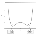
強誘電性の物質は、結晶化された物質構造において、単位セル(unit cell)内の電荷分布が、非中心対称(non-centrosymmetric)であり、自発的な電気双極子(electric dipole)、すなわち、自発分極(spontaneous polarization)を有する。強誘電性の物質は、外部電場がない状態においても、電気双極子による残留分極(remnant polarization)を有し、同時に、外部電場により、分極の方向がドメイン単位に反転(switching)されもする。
一方、反強誘電性物質の場合、そのようなヒステリシスがほとんど示されない。
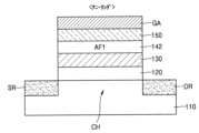
図8Aを参照すれば、チャネル領域CHを含む基板110が設けられる。
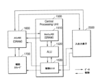
図9を参照すれば、1つのチップ1000に、メモリユニット1010、ALU(arithmetic logic unit)1020及び制御ユニット1030が形成されうる。同一基板上に、メモリユニット1010、ALU 1020及び制御ユニット1030をモノリシック(monolithic)に集積し、チップ1000を形成することができる。ALU 1020及び制御ユニット1030それぞれは、前述の実施形態のうちいずれか一つによるドメインスイッチング素子100,101,102を含むロジックトランジスタを含んでもよい。例えば、該ロジックトランジスタは、反強誘電性を有し、実質的に非履歴挙動特性を有するドメインスイッチング層を含んでもよい。メモリユニット1010は、メモリ素子を含んでもよい。例えば、前記メモリ素子は、強誘電ドメインを含みながら、履歴挙動特性を有するドメイン層を含んでもよい。メモリユニット1010、ALU 1020及び制御ユニット1030は、オンチップ(on-chip)において、メタルラインで相互連結され、直接通信することができる。メモリユニット1010は、メインメモリ及びキャッシュメモリをいずれも含んでもよい。そのようなチップ1000は、オンチップメモリ処理ユニット(on-chip memory processing unit)と言える。チップ1000と連結された入出力素子2000がさらに具備されうる。
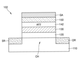
110 基板
120 誘電体層
130 バリア層
140 反強誘電層
142 ドメインスイッチング層
CH チャネル領域
DR ドレイン
GA ゲート電極
SR ソース
Claims (22)
- チャネル領域と、
前記チャネル領域に連結されたソース及びドレインと、
前記チャネル領域と離隔されるように配置されたゲート電極と、
前記チャネル領域と前記ゲート電極との間に配置された反強誘電層と、
前記ゲート電極と前記反強誘電層との間に、前記反強誘電層と接するように配置された伝導層と、
前記反強誘電層と前記チャネル領域との間に配置されたバリア層と、を含み、
前記伝導層の熱膨脹係数は、前記反強誘電層の熱膨脹係数より小さく、
前記反強誘電層は、前記反強誘電層に印加される引張り応力に基づいて反強誘電性を示す、ドメインスイッチング素子。 - 前記反強誘電層は、前記伝導層と隣接した少なくとも一部領域が結晶化された、請求項1に記載のドメインスイッチング素子。
- 前記反強誘電層は、前記伝導層との界面領域において、ZrOの比率が50%以上である、請求項1または2に記載のドメインスイッチング素子。
- 前記伝導層は、面抵抗が1MΩ/squareより小さい物質からなる、請求項1から3のいずれか一項に記載のドメインスイッチング素子。
- 前記伝導層の熱膨脹係数は、Moの熱膨脹係数より大きい、請求項1から4のいずれか一項に記載のドメインスイッチング素子。
- 前記伝導層は、窒化金属、酸窒化金属、RuO、MoOまたはWOを含む、請求項1から5のいずれか一項に記載のドメインスイッチング素子。
- 前記バリア層は、前記反強誘電層の降伏電圧より大きい降伏電圧を有する、請求項1から6のいずれか一項に記載のドメインスイッチング素子。
- 前記バリア層は、SiO、AlO、HfO、ZrO、LaO、YO、MgOのうち少なくとも一つを含むか、あるいはSiO、AlO、HfO、ZrO、LaO、YO、MgOのうちいずれか一つにドーパントがドーピングされた物質、または二次元絶縁体を含む、請求項1から7のいずれか一項に記載のドメインスイッチング素子。
- 前記バリア層と前記チャネル領域との間に配置された誘電体層をさらに含む、請求項1から8のいずれか一項に記載のドメインスイッチング素子。
- 前記誘電体層は、前記バリア層と異なる物質からなる、請求項9に記載のドメインスイッチング素子。
- 前記バリア層の誘電定数が前記誘電体層の誘電定数より大きい、請求項9または10に記載のドメインスイッチング素子。
- 前記誘電体層は、SiO、AlO、HfO、ZrO、または二次元絶縁体を含む、請求項9から11のいずれか一項に記載のドメインスイッチング素子。
- 前記反強誘電層は、HfO、ZrO、SiO、AlO、CeO、YO及びLaOのうち少なくとも一つを含む、請求項1から12のいずれか一項に記載のドメインスイッチング素子。
- 前記反強誘電層は、ドーパントをさらに含み、
前記ドーパントは、Si、Al、Zr、Y、La、Gd、Sr、Hf、Ceのうち少なくとも一つを含む、請求項13に記載のドメインスイッチング素子。 - 前記チャネル領域は、Si、Ge、SiGe、III-V族半導体、酸化物半導体、窒化物半導体、酸窒化物半導体、二次元物質、量子ドット、遷移金属ジカルコゲナイド及び有機半導体のうち少なくとも一つを含む、請求項1から14のいずれか一項に記載のドメインスイッチング素子。
- チャネル領域を含む基板を設ける段階と、
前記チャネル領域上に、バリア層、ドメインスイッチング層及び伝導層を含む積層構造を形成する段階と、
前記積層構造上に電極物質層を形成する段階と、
前記ドメインスイッチング層に反強誘電性を誘導する段階と、を含む、請求項1に記載のドメインスイッチング素子製造方法。 - 前記ドメインスイッチング層は、HfO、ZrO、SiO、AlO、CeO、YO、LaOのうち少なくとも一つを含む、請求項16に記載のドメインスイッチング素子製造方法。
- 前記伝導層は、窒化金属、酸窒化金属、RuO、MoOまたはWOを含む、請求項16または17に記載のドメインスイッチング素子製造方法。
- 前記誘導する段階は、
前記伝導層と隣接した前記ドメインスイッチング層の少なくとも一部領域を結晶化する段階を含む、請求項16から18のいずれか一項に記載のドメインスイッチング素子製造方法。 - 前記誘導する段階は、
前記伝導層により、前記ドメインスイッチング層に引張り応力が印加されるようにする段階を含む、請求項16から19のいずれか一項に記載のドメインスイッチング素子製造方法。 - 前記誘導する段階は、
前記積層構造を熱処理する段階を含む、請求項16から20のいずれか一項に記載のドメインスイッチング素子製造方法。 - 前記熱処理する段階は、
前記積層構造を形成する段階後、前記電極物質層を形成する以前に行われ、及び/または
前記電極物質層を形成する段階後に行われる、請求項21に記載のドメインスイッチング素子製造方法。
Applications Claiming Priority (2)
| Application Number | Priority Date | Filing Date | Title |
|---|---|---|---|
| KR10-2019-0117483 | 2019-09-24 | ||
| KR1020190117483A KR20210035553A (ko) | 2019-09-24 | 2019-09-24 | 도메인 스위칭 소자 및 그 제조방법 |
Publications (2)
| Publication Number | Publication Date |
|---|---|
| JP2021052184A JP2021052184A (ja) | 2021-04-01 |
| JP7601366B2 true JP7601366B2 (ja) | 2024-12-17 |
Family
ID=72615710
Family Applications (1)
| Application Number | Title | Priority Date | Filing Date |
|---|---|---|---|
| JP2020159660A Active JP7601366B2 (ja) | 2019-09-24 | 2020-09-24 | ドメインスイッチング素子及びその製造方法 |
Country Status (5)
| Country | Link |
|---|---|
| US (3) | US11527646B2 (ja) |
| EP (1) | EP3799131A1 (ja) |
| JP (1) | JP7601366B2 (ja) |
| KR (1) | KR20210035553A (ja) |
| CN (1) | CN112635561A (ja) |
Families Citing this family (11)
| Publication number | Priority date | Publication date | Assignee | Title |
|---|---|---|---|---|
| US11950429B2 (en) * | 2019-12-30 | 2024-04-02 | Samsung Electronics Co., Ltd. | Ferroelectric capacitors, transistors, memory devices, and methods of manufacturing ferroelectric devices |
| KR20210138997A (ko) * | 2020-05-13 | 2021-11-22 | 삼성전자주식회사 | 커패시터, 커패시터 제어 방법, 및 이를 포함하는 트랜지스터 |
| KR102825789B1 (ko) * | 2020-05-18 | 2025-06-26 | 에스케이하이닉스 주식회사 | 반도체 장치 |
| KR102815962B1 (ko) * | 2020-05-18 | 2025-06-04 | 에스케이하이닉스 주식회사 | 반도체 장치 |
| US12382670B2 (en) | 2020-11-04 | 2025-08-05 | Samsung Electronics Co., Ltd. | Thin film structure and semiconductor device comprising the same |
| EP4075481A1 (en) * | 2021-04-15 | 2022-10-19 | Terra Quantum AG | Field effect transistor with a negative capacitance gate structure |
| KR102881018B1 (ko) * | 2021-07-22 | 2025-11-03 | 삼성전자주식회사 | 반강유전 박막 구조체 및 이를 포함하는 전자 소자 |
| KR20230074349A (ko) * | 2021-11-19 | 2023-05-30 | 삼성전자주식회사 | 반도체 장치 |
| EP4203066A1 (en) * | 2021-12-21 | 2023-06-28 | IMEC vzw | Split gate ferrofet |
| CN114628583A (zh) * | 2022-02-25 | 2022-06-14 | 中国科学院微电子研究所 | 铁电存储器件及其制造方法 |
| KR102721720B1 (ko) * | 2022-07-18 | 2024-10-24 | 삼성전자주식회사 | 반도체 소자 및 이를 포함하는 전자 장치 |
Citations (5)
| Publication number | Priority date | Publication date | Assignee | Title |
|---|---|---|---|---|
| WO2009128133A1 (ja) | 2008-04-14 | 2009-10-22 | 富士通株式会社 | 反強誘電体ゲートトランジスタおよびその製造方法、不揮発性メモリ素子 |
| US20160284540A1 (en) | 2015-03-24 | 2016-09-29 | Globalfoundries Inc. | Devices comprising high-k dielectric layer and methods of forming same |
| JP2017518639A (ja) | 2014-05-20 | 2017-07-06 | マイクロン テクノロジー, インク. | 有極性、カイラル、非中心対称性強誘電体材料、その材料を含むメモリセルおよび関連するデバイスと方法。 |
| US20170365719A1 (en) | 2016-06-15 | 2017-12-21 | Taiwan Semiconductor Manufacturing Co., Ltd. | Negative Capacitance Field Effect Transistor |
| JP2019102797A (ja) | 2017-11-30 | 2019-06-24 | インテル・コーポレーション | 次世代型集積回路構造製造のためのトレンチコンタクト構造 |
Family Cites Families (46)
| Publication number | Priority date | Publication date | Assignee | Title |
|---|---|---|---|---|
| JP2001354497A (ja) | 2000-06-07 | 2001-12-25 | Matsushita Electric Ind Co Ltd | 強誘電体膜の製造方法 |
| JP2002110932A (ja) * | 2000-09-28 | 2002-04-12 | Toshiba Corp | 半導体装置及びその製造方法 |
| US7154779B2 (en) * | 2004-01-21 | 2006-12-26 | Sandisk Corporation | Non-volatile memory cell using high-k material inter-gate programming |
| JP2005244031A (ja) | 2004-02-27 | 2005-09-08 | Nec Electronics Corp | 半導体装置およびその製造方法 |
| US7217643B2 (en) * | 2005-02-24 | 2007-05-15 | Freescale Semiconductors, Inc. | Semiconductor structures and methods for fabricating semiconductor structures comprising high dielectric constant stacked structures |
| US20080079111A1 (en) * | 2006-09-29 | 2008-04-03 | Tokyo Electron Limited | Semiconductor devices containing nitrided high dielectric constant films |
| US7662693B2 (en) * | 2007-09-26 | 2010-02-16 | Micron Technology, Inc. | Lanthanide dielectric with controlled interfaces |
| TWI642113B (zh) * | 2008-08-08 | 2018-11-21 | 半導體能源研究所股份有限公司 | 半導體裝置的製造方法 |
| KR101026386B1 (ko) | 2009-05-06 | 2011-04-07 | 주식회사 하이닉스반도체 | 반도체 소자의 듀얼 폴리게이트 형성방법 |
| CN101593755B (zh) | 2009-06-17 | 2012-02-01 | 复旦大学 | 一种基于金属/反铁电薄膜/金属氧化物/半导体场效应管结构的存储器单元 |
| KR102362616B1 (ko) * | 2009-07-31 | 2022-02-15 | 가부시키가이샤 한도오따이 에네루기 켄큐쇼 | 표시 장치 |
| KR20120051727A (ko) * | 2009-07-31 | 2012-05-22 | 가부시키가이샤 한도오따이 에네루기 켄큐쇼 | 반도체 디바이스 및 그 형성 방법 |
| KR20250150667A (ko) * | 2010-02-26 | 2025-10-20 | 가부시키가이샤 한도오따이 에네루기 켄큐쇼 | 반도체 장치 |
| WO2011129456A1 (en) * | 2010-04-16 | 2011-10-20 | Semiconductor Energy Laboratory Co., Ltd. | Deposition method and method for manufacturing semiconductor device |
| KR101540039B1 (ko) * | 2010-04-23 | 2015-07-28 | 가부시키가이샤 한도오따이 에네루기 켄큐쇼 | 반도체 장치의 제작 방법 |
| US8476155B1 (en) | 2010-07-14 | 2013-07-02 | Samsung Electronics Co., Ltd. | Formation of a high-K crystalline dielectric composition |
| US9608101B2 (en) * | 2011-01-04 | 2017-03-28 | Ecole Polytechnique Federale De Lausanne (Epfl) | Semiconductor device |
| JP6226518B2 (ja) * | 2011-10-24 | 2017-11-08 | 株式会社半導体エネルギー研究所 | 半導体装置 |
| WO2013150920A1 (ja) * | 2012-04-05 | 2013-10-10 | 東京エレクトロン株式会社 | 半導体デバイスの製造方法及び基板処理システム |
| KR102173074B1 (ko) * | 2012-05-10 | 2020-11-02 | 가부시키가이샤 한도오따이 에네루기 켄큐쇼 | 반도체 장치 |
| KR102295737B1 (ko) * | 2012-05-10 | 2021-09-01 | 가부시키가이샤 한도오따이 에네루기 켄큐쇼 | 반도체 디바이스 |
| CN107591316B (zh) * | 2012-05-31 | 2021-06-08 | 株式会社半导体能源研究所 | 半导体装置 |
| JP2014042004A (ja) * | 2012-07-26 | 2014-03-06 | Semiconductor Energy Lab Co Ltd | 半導体装置及びその作製方法 |
| TWI782259B (zh) * | 2012-10-24 | 2022-11-01 | 日商半導體能源研究所股份有限公司 | 半導體裝置及其製造方法 |
| US9287411B2 (en) * | 2012-10-24 | 2016-03-15 | Semiconductor Energy Laboratory Co., Ltd. | Semiconductor device and method for manufacturing the same |
| US9190484B2 (en) * | 2013-01-18 | 2015-11-17 | Taiwan Semiconductor Manufacturing Company, Ltd. | Vertical tunneling field-effect transistor cell and fabricating the same |
| JP6121819B2 (ja) * | 2013-07-04 | 2017-04-26 | 株式会社東芝 | 半導体装置および誘電体膜 |
| US9064865B2 (en) | 2013-10-11 | 2015-06-23 | Taiwan Semiconductor Manufacturing Co., Ltd. | Mechanisms for forming gate dielectric layer |
| US9991392B2 (en) * | 2013-12-03 | 2018-06-05 | Semiconductor Energy Laboratory Co., Ltd. | Semiconductor device and manufacturing method thereof |
| US9269785B2 (en) * | 2014-01-27 | 2016-02-23 | Globalfoundries Inc. | Semiconductor device with ferroelectric hafnium oxide and method for forming semiconductor device |
| US9391162B2 (en) * | 2014-04-04 | 2016-07-12 | Taiwan Semiconductor Manufacturing Company, Ltd. | Tunnel MOSFET with ferroelectric gate stack |
| US9337334B2 (en) * | 2014-04-21 | 2016-05-10 | Globalfoundries Inc. | Semiconductor memory device employing a ferromagnetic gate |
| JP6676316B2 (ja) * | 2014-09-12 | 2020-04-08 | 株式会社半導体エネルギー研究所 | 半導体装置の作製方法 |
| US9349652B1 (en) * | 2014-12-12 | 2016-05-24 | Taiwan Semiconductor Manufacturing Company, Ltd. | Method of forming semiconductor device with different threshold voltages |
| DE102014018382B4 (de) * | 2014-12-15 | 2018-07-26 | Forschungszentrum Jülich GmbH | Tunnel-Feldeffekttransistor sowie Verfahren zu dessen Herstellung |
| US9653613B2 (en) * | 2015-02-27 | 2017-05-16 | Semiconductor Energy Laboratory Co., Ltd. | Semiconductor device and manufacturing method thereof |
| US9679893B2 (en) * | 2015-05-15 | 2017-06-13 | Taiwan Semiconductor Manufacturing Company Limited | Semiconductor device and transistor |
| JP6814915B2 (ja) | 2015-09-18 | 2021-01-20 | アドバンストマテリアルテクノロジーズ株式会社 | 強誘電体メモリ及びその製造方法、強誘電体膜及びその製造方法 |
| US9978868B2 (en) * | 2015-11-16 | 2018-05-22 | Taiwan Semiconductor Manufacturing Co., Ltd. | Negative capacitance field effect transistor with charged dielectric material |
| US9876018B2 (en) * | 2015-12-03 | 2018-01-23 | Micron Technology, Inc. | Ferroelectric capacitor, ferroelectric field effect transistor, and method used in forming an electronic component comprising conductive material and ferroelectric material |
| US10090036B2 (en) * | 2015-12-21 | 2018-10-02 | Imec Vzw | Non-volatile memory cell having pinch-off ferroelectric field effect transistor |
| US10115796B2 (en) * | 2016-01-07 | 2018-10-30 | Taiwan Semiconductor Manufacturing Company, Ltd. | Method of pulling-back sidewall metal layer |
| DE102017200678B4 (de) * | 2016-01-19 | 2019-06-27 | Fraunhofer-Gesellschaft zur Förderung der angewandten Forschung e.V. | Verfahren zur Herstellung einer Mikroelektronikschaltung sowie entsprechende Mikroelektronikschaltung |
| US20170345831A1 (en) | 2016-05-25 | 2017-11-30 | Micron Technology, Inc. | Ferroelectric Devices and Methods of Forming Ferroelectric Devices |
| US9853150B1 (en) * | 2016-08-15 | 2017-12-26 | Taiwan Semiconductor Manufacturing Co., Ltd. | Method of fabricating epitaxial gate dielectrics and semiconductor device of the same |
| KR20190001455A (ko) * | 2017-06-27 | 2019-01-04 | 에스케이하이닉스 주식회사 | 강유전성 메모리 장치 |
-
2019
- 2019-09-24 KR KR1020190117483A patent/KR20210035553A/ko active Pending
-
2020
- 2020-09-21 US US17/026,665 patent/US11527646B2/en active Active
- 2020-09-23 EP EP20197678.4A patent/EP3799131A1/en active Pending
- 2020-09-24 CN CN202011013829.7A patent/CN112635561A/zh active Pending
- 2020-09-24 JP JP2020159660A patent/JP7601366B2/ja active Active
-
2022
- 2022-11-30 US US18/060,372 patent/US11824119B2/en active Active
-
2023
- 2023-10-13 US US18/486,493 patent/US12224346B2/en active Active
Patent Citations (5)
| Publication number | Priority date | Publication date | Assignee | Title |
|---|---|---|---|---|
| WO2009128133A1 (ja) | 2008-04-14 | 2009-10-22 | 富士通株式会社 | 反強誘電体ゲートトランジスタおよびその製造方法、不揮発性メモリ素子 |
| JP2017518639A (ja) | 2014-05-20 | 2017-07-06 | マイクロン テクノロジー, インク. | 有極性、カイラル、非中心対称性強誘電体材料、その材料を含むメモリセルおよび関連するデバイスと方法。 |
| US20160284540A1 (en) | 2015-03-24 | 2016-09-29 | Globalfoundries Inc. | Devices comprising high-k dielectric layer and methods of forming same |
| US20170365719A1 (en) | 2016-06-15 | 2017-12-21 | Taiwan Semiconductor Manufacturing Co., Ltd. | Negative Capacitance Field Effect Transistor |
| JP2019102797A (ja) | 2017-11-30 | 2019-06-24 | インテル・コーポレーション | 次世代型集積回路構造製造のためのトレンチコンタクト構造 |
Also Published As
| Publication number | Publication date |
|---|---|
| US12224346B2 (en) | 2025-02-11 |
| US20230100991A1 (en) | 2023-03-30 |
| CN112635561A (zh) | 2021-04-09 |
| KR20210035553A (ko) | 2021-04-01 |
| JP2021052184A (ja) | 2021-04-01 |
| EP3799131A1 (en) | 2021-03-31 |
| US11824119B2 (en) | 2023-11-21 |
| US20240038890A1 (en) | 2024-02-01 |
| US11527646B2 (en) | 2022-12-13 |
| US20210091227A1 (en) | 2021-03-25 |
Similar Documents
| Publication | Publication Date | Title |
|---|---|---|
| JP7601366B2 (ja) | ドメインスイッチング素子及びその製造方法 | |
| JP7566397B2 (ja) | ロジックスイッチング素子及びその製造方法 | |
| US12107140B2 (en) | Thin film structure and semiconductor device including the same | |
| US12382670B2 (en) | Thin film structure and semiconductor device comprising the same | |
| KR102778194B1 (ko) | 로직 스위칭 소자 및 그 제조방법 | |
| US20220285374A1 (en) | Wakeup free approach to improve the ferroelectricity of feram using a stressor layer | |
| CN114447223A (zh) | 半导体器件和包括其的半导体装置 | |
| US20230062878A1 (en) | Electronic device including ferroelectric thin film structure | |
| US20230068904A1 (en) | Electronic device including ferroelectric thin film structure | |
| EP4008810A2 (en) | Fluorite-based material thin film and semiconductor device comprising the same | |
| CN115440805A (zh) | 薄膜结构、包括其的半导体器件、晶体管以及半导体装置 | |
| KR20220077051A (ko) | fluorite계 물질 박막 및 이를 포함하는 반도체 소자 | |
| US20230282389A1 (en) | Thin-film structure and semiconductor device comprising the same | |
| KR102881016B1 (ko) | 박막 구조체 및 이를 포함하는 반도체 소자 | |
| KR20250101479A (ko) | 반도체 소자 및 이를 포함하는 전자 장치 | |
| US20240194761A1 (en) | Electronic device and electronic apparatus including the same | |
| KR20250106688A (ko) | 반도체 소자 | |
| KR20240068207A (ko) | 도메인 조절된 강유전체 재료를 포함하는 전계 효과 트랜지스터, 커패시터, 및 전자 장치 |
Legal Events
| Date | Code | Title | Description |
|---|---|---|---|
| A621 | Written request for application examination |
Free format text: JAPANESE INTERMEDIATE CODE: A621 Effective date: 20230818 |
|
| A977 | Report on retrieval |
Free format text: JAPANESE INTERMEDIATE CODE: A971007 Effective date: 20240725 |
|
| A131 | Notification of reasons for refusal |
Free format text: JAPANESE INTERMEDIATE CODE: A131 Effective date: 20240805 |
|
| A521 | Request for written amendment filed |
Free format text: JAPANESE INTERMEDIATE CODE: A523 Effective date: 20241028 |
|
| TRDD | Decision of grant or rejection written | ||
| A01 | Written decision to grant a patent or to grant a registration (utility model) |
Free format text: JAPANESE INTERMEDIATE CODE: A01 Effective date: 20241105 |
|
| A61 | First payment of annual fees (during grant procedure) |
Free format text: JAPANESE INTERMEDIATE CODE: A61 Effective date: 20241128 |
|
| R150 | Certificate of patent or registration of utility model |
Ref document number: 7601366 Country of ref document: JP Free format text: JAPANESE INTERMEDIATE CODE: R150 |