JP7581374B2 - 基板処理システム及び基板処理方法 - Google Patents
基板処理システム及び基板処理方法 Download PDFInfo
- Publication number
- JP7581374B2 JP7581374B2 JP2022565233A JP2022565233A JP7581374B2 JP 7581374 B2 JP7581374 B2 JP 7581374B2 JP 2022565233 A JP2022565233 A JP 2022565233A JP 2022565233 A JP2022565233 A JP 2022565233A JP 7581374 B2 JP7581374 B2 JP 7581374B2
- Authority
- JP
- Japan
- Prior art keywords
- substrate
- thickness
- wafer
- processing
- grinding
- Prior art date
- Legal status (The legal status is an assumption and is not a legal conclusion. Google has not performed a legal analysis and makes no representation as to the accuracy of the status listed.)
- Active
Links
Images


Classifications
-
- B—PERFORMING OPERATIONS; TRANSPORTING
- B24—GRINDING; POLISHING
- B24B—MACHINES, DEVICES, OR PROCESSES FOR GRINDING OR POLISHING; DRESSING OR CONDITIONING OF ABRADING SURFACES; FEEDING OF GRINDING, POLISHING, OR LAPPING AGENTS
- B24B37/00—Lapping machines or devices; Accessories
- B24B37/005—Control means for lapping machines or devices
-
- B—PERFORMING OPERATIONS; TRANSPORTING
- B24—GRINDING; POLISHING
- B24B—MACHINES, DEVICES, OR PROCESSES FOR GRINDING OR POLISHING; DRESSING OR CONDITIONING OF ABRADING SURFACES; FEEDING OF GRINDING, POLISHING, OR LAPPING AGENTS
- B24B41/00—Component parts such as frames, beds, carriages, headstocks
- B24B41/06—Work supports, e.g. adjustable steadies
-
- B—PERFORMING OPERATIONS; TRANSPORTING
- B24—GRINDING; POLISHING
- B24B—MACHINES, DEVICES, OR PROCESSES FOR GRINDING OR POLISHING; DRESSING OR CONDITIONING OF ABRADING SURFACES; FEEDING OF GRINDING, POLISHING, OR LAPPING AGENTS
- B24B49/00—Measuring or gauging equipment for controlling the feed movement of the grinding tool or work; Arrangements of indicating or measuring equipment, e.g. for indicating the start of the grinding operation
- B24B49/02—Measuring or gauging equipment for controlling the feed movement of the grinding tool or work; Arrangements of indicating or measuring equipment, e.g. for indicating the start of the grinding operation according to the instantaneous size and required size of the workpiece acted upon, the measuring or gauging being continuous or intermittent
-
- B—PERFORMING OPERATIONS; TRANSPORTING
- B24—GRINDING; POLISHING
- B24B—MACHINES, DEVICES, OR PROCESSES FOR GRINDING OR POLISHING; DRESSING OR CONDITIONING OF ABRADING SURFACES; FEEDING OF GRINDING, POLISHING, OR LAPPING AGENTS
- B24B55/00—Safety devices for grinding or polishing machines; Accessories fitted to grinding or polishing machines for keeping tools or parts of the machine in good working condition
- B24B55/06—Dust extraction equipment on grinding or polishing machines
-
- B—PERFORMING OPERATIONS; TRANSPORTING
- B24—GRINDING; POLISHING
- B24B—MACHINES, DEVICES, OR PROCESSES FOR GRINDING OR POLISHING; DRESSING OR CONDITIONING OF ABRADING SURFACES; FEEDING OF GRINDING, POLISHING, OR LAPPING AGENTS
- B24B7/00—Machines or devices designed for grinding plane surfaces on work, including polishing plane glass surfaces; Accessories therefor
- B24B7/04—Machines or devices designed for grinding plane surfaces on work, including polishing plane glass surfaces; Accessories therefor involving a rotary work-table
-
- H—ELECTRICITY
- H10—SEMICONDUCTOR DEVICES; ELECTRIC SOLID-STATE DEVICES NOT OTHERWISE PROVIDED FOR
- H10P—GENERIC PROCESSES OR APPARATUS FOR THE MANUFACTURE OR TREATMENT OF DEVICES COVERED BY CLASS H10
- H10P52/00—Grinding, lapping or polishing of wafers, substrates or parts of devices
-
- H—ELECTRICITY
- H10—SEMICONDUCTOR DEVICES; ELECTRIC SOLID-STATE DEVICES NOT OTHERWISE PROVIDED FOR
- H10P—GENERIC PROCESSES OR APPARATUS FOR THE MANUFACTURE OR TREATMENT OF DEVICES COVERED BY CLASS H10
- H10P72/00—Handling or holding of wafers, substrates or devices during manufacture or treatment thereof
- H10P72/04—Apparatus for manufacture or treatment
- H10P72/0428—Apparatus for mechanical treatment or grinding or cutting
-
- H—ELECTRICITY
- H10—SEMICONDUCTOR DEVICES; ELECTRIC SOLID-STATE DEVICES NOT OTHERWISE PROVIDED FOR
- H10P—GENERIC PROCESSES OR APPARATUS FOR THE MANUFACTURE OR TREATMENT OF DEVICES COVERED BY CLASS H10
- H10P72/00—Handling or holding of wafers, substrates or devices during manufacture or treatment thereof
- H10P72/70—Handling or holding of wafers, substrates or devices during manufacture or treatment thereof for supporting or gripping
-
- H—ELECTRICITY
- H10—SEMICONDUCTOR DEVICES; ELECTRIC SOLID-STATE DEVICES NOT OTHERWISE PROVIDED FOR
- H10P—GENERIC PROCESSES OR APPARATUS FOR THE MANUFACTURE OR TREATMENT OF DEVICES COVERED BY CLASS H10
- H10P74/00—Testing or measuring during manufacture or treatment of wafers, substrates or devices
Landscapes
- Engineering & Computer Science (AREA)
- Mechanical Engineering (AREA)
- Mechanical Treatment Of Semiconductor (AREA)
- Container, Conveyance, Adherence, Positioning, Of Wafer (AREA)
- Cleaning Or Drying Semiconductors (AREA)
- Constituent Portions Of Griding Lathes, Driving, Sensing And Control (AREA)
- Grinding Of Cylindrical And Plane Surfaces (AREA)
- Grinding-Machine Dressing And Accessory Apparatuses (AREA)
Description
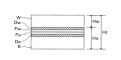
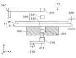
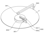
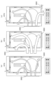
一方、図11(a)に示すように、部分厚み測定部340による測定点P1での上ウェハWの厚みHwの測定に際しては、センサ341とチャック300の干渉が生じないため、チャック300(重合ウェハT)は回転させてもよいし、回転を停止させてもよい。
また、図11(b)に示すように、部分厚み測定部340による測定点P2での上ウェハWの厚みHwの測定に際しても、チャック300を回転させながら、上ウェハWの厚みHwを周方向に複数点で測定する。
そして、測定点P2において、測定された周方向の複数点の移動平均値を算出し、当該測定点P2における重合ウェハTの全体厚みHt、又は上ウェハWの厚みHwとする。なお、測定点P2における測定厚みは、周方向の複数点の移動中央値としてもよい。
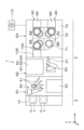
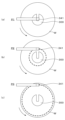
また、図12(b)に示すように、第1シャッタ350を開放した場合、排気部370からのみ気流が排出される。
更に、図12(c)に示すように、第2シャッタ360を開放した場合、当該第2シャッタ360側から第1厚み測定装置52への気流の流入は発生せず、また、第1シャッタ350側から第1厚み測定装置52の外部への気流の流出も発生しない。
また、第1厚み測定装置52からは、第2シャッタ360(加工装置70)側及び排気部370のみから気流が流出し、第1シャッタ350(第1処理ブロックG1)側へは気流が流出しない。すなわち、清浄空間である第1処理ブロックG1にパーティクル等が流出することが抑制される。
また更に、図12に示したように第1厚み測定装置52においては、第1シャッタ350と第2シャッタ360とが同時に開放されるタイミングを作らない。これにより、加工装置70から第1処理ブロックG1にパーティクル等が流出することが更に抑制される。
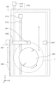
52 第1厚み測定装置
53 第2厚み測定装置
70 加工装置
Ht 全体厚み
Hw (上ウェハの)厚み
S 下ウェハ
T 重合ウェハ
W 上ウェハ
Claims (18)
- 第1基板と第2基板が接合された重合基板を処理する基板処理システムであって、
前記第1基板を研削する加工装置と、
前記加工装置の外部に設けられ、研削前の前記第1基板の厚みと当該第1基板を含む前記重合基板の全体厚みを測定する第1厚み測定装置と、
前記加工装置の外部に設けられ、研削後の前記第1基板の厚みを測定する第2厚み測定装置と、を備える、基板処理システム。
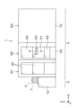
- 前記第1厚み測定装置は、
前記重合基板を保持する第1基板保持部と、
前記第1基板保持部に保持された前記第1基板の厚みを測定する第1測定部と、
前記第1基板保持部に保持された前記重合基板の全体厚みを測定する全体厚み測定部と、を備え、
前記第1基板保持部には、当該第1基板保持部の中心部から外端部まで径方向に延伸し、前記全体厚み測定部が相対的に進退自在な切り欠き部が形成されており、
前記第2厚み測定装置は、
前記重合基板を保持する第2基板保持部と、
前記第2基板保持部に保持された前記第1基板の厚みを測定する第2測定部と、を備える、請求項1に記載の基板処理システム。 - 前記第1基板保持部の径は、前記第2基板保持部の径よりも小さい、請求項2に記載の基板処理システム。
- 前記第1厚み測定装置は、
前記第1基板保持部を水平方向に移動及び回転させる第1駆動部と、
前記加工装置で研削前の前記重合基板の水平方向位置を検出する第1位置検出部を備え、
前記第1位置検出部は、前記第1基板保持部の移動方向において、前記第1測定部と同じ位置に配置される、請求項2又は3に記載の基板処理システム。 - 前記第2厚み測定装置は、
前記第2基板保持部を水平方向に移動及び回転させる第2駆動部と、
研削後の前記重合基板の水平方向位置を検出する第2位置検出部を備え、
前記第2位置検出部は、前記第2基板保持部の移動方向において、前記第2測定部と同じ位置に配置される、請求項2~4のいずれか一項に記載の基板処理システム。 - 複数の前記重合基板を収容可能なカセットに対して前記重合基板を搬送する第1基板搬送装置と、
前記加工装置に対して前記重合基板を搬送する第2基板搬送装置と、を備え、
前記第1厚み測定装置には、
前記第1基板搬送装置が進入する第1搬送口と、
前記第2基板搬送装置が進入する第2搬送口と、が形成され、
前記第2厚み測定装置には、
前記第1基板搬送装置が進入する第1搬送口が形成され、
前記第2基板搬送装置が進入する第2搬送口は形成されない、請求項1~5のいずれか一項に記載の基板処理システム。 - 複数の前記重合基板を収容可能なカセットが載置される搬入出領域と、
前記第1厚み測定装置及び前記第2厚み測定装置が設けられる処理領域と、
前記加工装置が設けられる加工領域と、が形成され、
前記搬入出領域の内部圧力を前記処理領域の内部圧力よりも高く、かつ、前記処理領域の内部圧力を前記加工領域の内部圧力よりも高く、制御する制御装置を備える、請求項1~6のいずれか一項に記載の基板処理システム。 - 前記制御装置は、前記第1厚み測定装置及び前記第2厚み測定装置の内部圧力を前記搬入出領域よりも低く、かつ、前記処理領域の内部圧力よりも高く、制御する、請求項7に記載の基板処理システム。
- 前記加工装置で研削前の前記重合基板を洗浄する第1洗浄装置と、
前記加工装置で研削後の前記重合基板を洗浄する第2洗浄装置と、を備え、
前記第1洗浄装置、前記第2洗浄装置、前記第1厚み測定装置及び前記第2厚み測定装置が積層して配置される、請求項1~8のいずれか一項に記載の基板処理システム。 - 基板処理システムにおいて第1基板と第2基板が接合された重合基板を処理する基板処理方法であって、
研削前の前記第1基板の厚みを第1厚み測定装置で測定することと、
研削前の前記重合基板の全体厚みを第1厚み測定装置で測定することと、
前記第1基板を加工装置で研削することと、
研削後の前記第1基板の厚みを第2厚み測定装置で測定することと、を含み、
前記第1厚み測定装置と前記第2厚み測定装置は、前記加工装置の外部に設けられている、基板処理方法。
- 研削前の前記重合基板の全体厚み、及び研削前の前記第1基板の厚みに基づいて前記第2基板の厚みを算出することと、
前記第1基板の研削に先立ち、算出された前記第2基板の厚みに基づいて、前記加工装置における第3基板保持部の前記重合基板の保持面と、研削砥石の研削面との相対的な傾きを調整することと、を含む請求項10に記載の基板処理方法。 - 前記基板処理システムにおいては、複数の重合基板が連続的に処理され、
次に処理される重合基板における前記第1基板の研削に先立ち、一の基板で測定された研削後の前記第1基板の厚みに基づいて、前記加工装置における第3基板保持部の前記重合基板の保持面と、研削砥石の研削面との相対的な傾きを調整する、請求項10または11に記載の基板処理方法。 - 研削前の前記重合基板の水平方向位置を第1厚み測定装置で検出することと、
研削後の前記重合基板の水平方向位置を第2厚み測定装置で検出することと、を含む請求項10~12のいずれか一項に記載の基板処理方法。 - 第1厚み測定装置及び前記第2厚み測定装置では、前記第1基板の厚みを径方向に複数点で測定し、
前記第1基板の中心部における厚みの測定を、前記水平方向位置の検出と同じ位置で行う、請求項13に記載の基板処理方法。 - 前記基板処理システムは、
複数の前記重合基板を収容可能なカセットに対して前記重合基板を搬送する第1基板搬送装置と、
前記加工装置に対して前記重合基板を搬送する第2基板搬送装置と、を備え、
前記第1厚み測定装置には、前記第1基板搬送装置及び前記第2基板搬送装置を進入させ、
前記第2厚み測定装置には、前記第1基板搬送装置のみを進入させて前記第2基板搬送装置は進入させない、請求項10~14のいずれか一項に記載の基板処理方法。 - 前記基板処理システムには、
複数の前記重合基板を収容可能なカセットが載置される搬入出領域と、
前記第1厚み測定装置及び前記第2厚み測定装置が設けられる処理領域と、
前記加工装置が設けられる加工領域と、が形成され、
前記搬入出領域の内部圧力を前記処理領域の内部圧力よりも高く、かつ、前記処理領域の内部圧力を前記加工領域の内部圧力よりも高く、制御する、請求項10~15のいずれか一項に記載の基板処理方法。 - 前記第1厚み測定装置及び前記第2厚み測定装置の内部圧力を前記搬入出領域よりも低く、かつ、前記処理領域の内部圧力よりも高く、制御する、請求項16に記載の基板処理方法。
- 前記第1厚み測定装置での前記第1基板の厚みの測定に先立って、研削前の前記重合基板を第1洗浄装置で洗浄することと、
前記第2厚み測定装置での前記第1基板の厚みの測定に先立って、研削後の前記重合基板を第2洗浄装置で洗浄することと、を含む、請求項10~17のいずれか一項に記載の基板処理方法。
Applications Claiming Priority (3)
| Application Number | Priority Date | Filing Date | Title |
|---|---|---|---|
| JP2020196956 | 2020-11-27 | ||
| JP2020196956 | 2020-11-27 | ||
| PCT/JP2021/041879 WO2022113795A1 (ja) | 2020-11-27 | 2021-11-15 | 基板処理システム及び基板処理方法 |
Publications (3)
| Publication Number | Publication Date |
|---|---|
| JPWO2022113795A1 JPWO2022113795A1 (ja) | 2022-06-02 |
| JPWO2022113795A5 JPWO2022113795A5 (ja) | 2023-08-08 |
| JP7581374B2 true JP7581374B2 (ja) | 2024-11-12 |
Family
ID=81755980
Family Applications (1)
| Application Number | Title | Priority Date | Filing Date |
|---|---|---|---|
| JP2022565233A Active JP7581374B2 (ja) | 2020-11-27 | 2021-11-15 | 基板処理システム及び基板処理方法 |
Country Status (5)
| Country | Link |
|---|---|
| US (1) | US20240017375A1 (ja) |
| JP (1) | JP7581374B2 (ja) |
| KR (1) | KR102928179B1 (ja) |
| CN (1) | CN116529026B (ja) |
| WO (1) | WO2022113795A1 (ja) |
Families Citing this family (1)
| Publication number | Priority date | Publication date | Assignee | Title |
|---|---|---|---|---|
| WO2026034231A1 (ja) * | 2024-08-07 | 2026-02-12 | 東京エレクトロン株式会社 | 基板加工方法、及び基板加工システム |
Citations (7)
| Publication number | Priority date | Publication date | Assignee | Title |
|---|---|---|---|---|
| JP2009274139A (ja) | 2008-05-12 | 2009-11-26 | Ebara Corp | 研磨方法及び研磨装置、並びに研磨装置制御用プログラム |
| JP2012033585A (ja) | 2010-07-29 | 2012-02-16 | Covalent Materials Corp | 研磨装置及び研磨方法 |
| JP2014226749A (ja) | 2013-05-22 | 2014-12-08 | 株式会社ディスコ | 研削方法 |
| JP2017056523A (ja) | 2015-09-17 | 2017-03-23 | 株式会社ディスコ | 研削装置 |
| JP2017113811A (ja) | 2015-12-21 | 2017-06-29 | 株式会社ディスコ | 研削装置 |
| WO2018235619A1 (ja) | 2017-06-21 | 2018-12-27 | 東京エレクトロン株式会社 | 基板処理システム、基板処理方法及びコンピュータ記憶媒体 |
| JP2021084146A (ja) | 2019-11-26 | 2021-06-03 | 株式会社ディスコ | ウェーハの研削方法 |
Family Cites Families (12)
| Publication number | Priority date | Publication date | Assignee | Title |
|---|---|---|---|---|
| US7457680B2 (en) * | 2000-12-27 | 2008-11-25 | Tokyo Electron Limited | Conveyance method for transporting objects |
| JP2003273050A (ja) * | 2002-03-15 | 2003-09-26 | Toshiba Ceramics Co Ltd | 研磨装置 |
| KR20070118617A (ko) * | 2005-04-04 | 2007-12-17 | 신에쯔 한도타이 가부시키가이샤 | 접합 웨이퍼의 제조방법 및 접합 웨이퍼 및 평면 연삭장치 |
| EP1872392B1 (en) * | 2005-04-19 | 2012-02-22 | Ebara Corporation | Substrate processing apparatus |
| JP2008264913A (ja) | 2007-04-18 | 2008-11-06 | Disco Abrasive Syst Ltd | 研削加工装置 |
| JP2009039827A (ja) * | 2007-08-09 | 2009-02-26 | Fujitsu Ltd | 研磨装置、基板及び電子機器の製造方法 |
| JP6051632B2 (ja) * | 2011-07-20 | 2016-12-27 | 日立化成株式会社 | 研磨剤及び基板の研磨方法 |
| JP6374169B2 (ja) * | 2014-01-23 | 2018-08-15 | 株式会社荏原製作所 | 研磨方法および研磨装置 |
| JP2018054500A (ja) * | 2016-09-29 | 2018-04-05 | 東京エレクトロン株式会社 | 位置検出システム及び処理装置 |
| JP6968201B2 (ja) * | 2017-12-22 | 2021-11-17 | 東京エレクトロン株式会社 | 基板処理システム、基板処理方法及びコンピュータ記憶媒体 |
| JP7242141B2 (ja) * | 2019-06-24 | 2023-03-20 | 株式会社ディスコ | 被加工物の加工方法 |
| JP7358185B2 (ja) * | 2019-10-15 | 2023-10-10 | 株式会社ディスコ | 厚み計測装置、及び厚み計測装置を備えた加工装置 |
-
2021
- 2021-11-15 CN CN202180077965.9A patent/CN116529026B/zh active Active
- 2021-11-15 KR KR1020237021209A patent/KR102928179B1/ko active Active
- 2021-11-15 JP JP2022565233A patent/JP7581374B2/ja active Active
- 2021-11-15 US US18/254,608 patent/US20240017375A1/en active Pending
- 2021-11-15 WO PCT/JP2021/041879 patent/WO2022113795A1/ja not_active Ceased
Patent Citations (7)
| Publication number | Priority date | Publication date | Assignee | Title |
|---|---|---|---|---|
| JP2009274139A (ja) | 2008-05-12 | 2009-11-26 | Ebara Corp | 研磨方法及び研磨装置、並びに研磨装置制御用プログラム |
| JP2012033585A (ja) | 2010-07-29 | 2012-02-16 | Covalent Materials Corp | 研磨装置及び研磨方法 |
| JP2014226749A (ja) | 2013-05-22 | 2014-12-08 | 株式会社ディスコ | 研削方法 |
| JP2017056523A (ja) | 2015-09-17 | 2017-03-23 | 株式会社ディスコ | 研削装置 |
| JP2017113811A (ja) | 2015-12-21 | 2017-06-29 | 株式会社ディスコ | 研削装置 |
| WO2018235619A1 (ja) | 2017-06-21 | 2018-12-27 | 東京エレクトロン株式会社 | 基板処理システム、基板処理方法及びコンピュータ記憶媒体 |
| JP2021084146A (ja) | 2019-11-26 | 2021-06-03 | 株式会社ディスコ | ウェーハの研削方法 |
Also Published As
| Publication number | Publication date |
|---|---|
| JPWO2022113795A1 (ja) | 2022-06-02 |
| WO2022113795A1 (ja) | 2022-06-02 |
| CN116529026B (zh) | 2025-11-25 |
| CN116529026A (zh) | 2023-08-01 |
| KR20230107685A (ko) | 2023-07-17 |
| KR102928179B1 (ko) | 2026-02-20 |
| US20240017375A1 (en) | 2024-01-18 |
Similar Documents
| Publication | Publication Date | Title |
|---|---|---|
| JP7516528B2 (ja) | 厚み測定装置及び厚み測定方法 | |
| TWI386989B (zh) | 研磨裝置及研磨方法 | |
| JP6937370B2 (ja) | 研削装置、研削方法及びコンピュータ記憶媒体 | |
| KR102450002B1 (ko) | 기판 처리 시스템, 기판 처리 방법 및 컴퓨터 기억 매체 | |
| JP4762647B2 (ja) | 研磨装置及び研磨方法 | |
| US12290898B2 (en) | Substrate processing method and substrate processing apparatus | |
| JP7018452B2 (ja) | 基板処理システム、基板処理方法及びコンピュータ記憶媒体 | |
| JP6584532B2 (ja) | 研削装置および研削方法 | |
| JP7071818B2 (ja) | 基板処理システム | |
| JP7581374B2 (ja) | 基板処理システム及び基板処理方法 | |
| JP2020110871A (ja) | 基板処理装置および基板処理装置において部分研磨されるべき領域を特定する方法 | |
| JP2022085344A (ja) | 基板処理システム及び基板処理方法 | |
| JP7653269B2 (ja) | 処理方法及び処理装置 | |
| JP7434352B2 (ja) | 基板処理方法及び基板処理装置 | |
| JP2022046137A (ja) | 基板処理方法及び基板処理システム | |
| WO2025027806A1 (ja) | 研削装置及び研削方法 |
Legal Events
| Date | Code | Title | Description |
|---|---|---|---|
| A521 | Request for written amendment filed |
Free format text: JAPANESE INTERMEDIATE CODE: A523 Effective date: 20230515 |
|
| A621 | Written request for application examination |
Free format text: JAPANESE INTERMEDIATE CODE: A621 Effective date: 20230515 |
|
| A131 | Notification of reasons for refusal |
Free format text: JAPANESE INTERMEDIATE CODE: A131 Effective date: 20240625 |
|
| A521 | Request for written amendment filed |
Free format text: JAPANESE INTERMEDIATE CODE: A523 Effective date: 20240820 |
|
| TRDD | Decision of grant or rejection written | ||
| A01 | Written decision to grant a patent or to grant a registration (utility model) |
Free format text: JAPANESE INTERMEDIATE CODE: A01 Effective date: 20241001 |
|
| A61 | First payment of annual fees (during grant procedure) |
Free format text: JAPANESE INTERMEDIATE CODE: A61 Effective date: 20241030 |
|
| R150 | Certificate of patent or registration of utility model |
Ref document number: 7581374 Country of ref document: JP Free format text: JAPANESE INTERMEDIATE CODE: R150 |