JP7581374B2 - SUBSTRATE PROCESSING SYSTEM AND SUBSTRATE PROCESSING METHOD - Google Patents
SUBSTRATE PROCESSING SYSTEM AND SUBSTRATE PROCESSING METHOD Download PDFInfo
- Publication number
- JP7581374B2 JP7581374B2 JP2022565233A JP2022565233A JP7581374B2 JP 7581374 B2 JP7581374 B2 JP 7581374B2 JP 2022565233 A JP2022565233 A JP 2022565233A JP 2022565233 A JP2022565233 A JP 2022565233A JP 7581374 B2 JP7581374 B2 JP 7581374B2
- Authority
- JP
- Japan
- Prior art keywords
- substrate
- thickness
- wafer
- processing
- grinding
- Prior art date
- Legal status (The legal status is an assumption and is not a legal conclusion. Google has not performed a legal analysis and makes no representation as to the accuracy of the status listed.)
- Active
Links
Images


Classifications
-
- B—PERFORMING OPERATIONS; TRANSPORTING
- B24—GRINDING; POLISHING
- B24B—MACHINES, DEVICES, OR PROCESSES FOR GRINDING OR POLISHING; DRESSING OR CONDITIONING OF ABRADING SURFACES; FEEDING OF GRINDING, POLISHING, OR LAPPING AGENTS
- B24B37/00—Lapping machines or devices; Accessories
- B24B37/005—Control means for lapping machines or devices
-
- B—PERFORMING OPERATIONS; TRANSPORTING
- B24—GRINDING; POLISHING
- B24B—MACHINES, DEVICES, OR PROCESSES FOR GRINDING OR POLISHING; DRESSING OR CONDITIONING OF ABRADING SURFACES; FEEDING OF GRINDING, POLISHING, OR LAPPING AGENTS
- B24B41/00—Component parts such as frames, beds, carriages, headstocks
- B24B41/06—Work supports, e.g. adjustable steadies
-
- B—PERFORMING OPERATIONS; TRANSPORTING
- B24—GRINDING; POLISHING
- B24B—MACHINES, DEVICES, OR PROCESSES FOR GRINDING OR POLISHING; DRESSING OR CONDITIONING OF ABRADING SURFACES; FEEDING OF GRINDING, POLISHING, OR LAPPING AGENTS
- B24B49/00—Measuring or gauging equipment for controlling the feed movement of the grinding tool or work; Arrangements of indicating or measuring equipment, e.g. for indicating the start of the grinding operation
- B24B49/02—Measuring or gauging equipment for controlling the feed movement of the grinding tool or work; Arrangements of indicating or measuring equipment, e.g. for indicating the start of the grinding operation according to the instantaneous size and required size of the workpiece acted upon, the measuring or gauging being continuous or intermittent
-
- B—PERFORMING OPERATIONS; TRANSPORTING
- B24—GRINDING; POLISHING
- B24B—MACHINES, DEVICES, OR PROCESSES FOR GRINDING OR POLISHING; DRESSING OR CONDITIONING OF ABRADING SURFACES; FEEDING OF GRINDING, POLISHING, OR LAPPING AGENTS
- B24B55/00—Safety devices for grinding or polishing machines; Accessories fitted to grinding or polishing machines for keeping tools or parts of the machine in good working condition
- B24B55/06—Dust extraction equipment on grinding or polishing machines
-
- B—PERFORMING OPERATIONS; TRANSPORTING
- B24—GRINDING; POLISHING
- B24B—MACHINES, DEVICES, OR PROCESSES FOR GRINDING OR POLISHING; DRESSING OR CONDITIONING OF ABRADING SURFACES; FEEDING OF GRINDING, POLISHING, OR LAPPING AGENTS
- B24B7/00—Machines or devices designed for grinding plane surfaces on work, including polishing plane glass surfaces; Accessories therefor
- B24B7/04—Machines or devices designed for grinding plane surfaces on work, including polishing plane glass surfaces; Accessories therefor involving a rotary work-table
-
- H—ELECTRICITY
- H10—SEMICONDUCTOR DEVICES; ELECTRIC SOLID-STATE DEVICES NOT OTHERWISE PROVIDED FOR
- H10P—GENERIC PROCESSES OR APPARATUS FOR THE MANUFACTURE OR TREATMENT OF DEVICES COVERED BY CLASS H10
- H10P52/00—Grinding, lapping or polishing of wafers, substrates or parts of devices
-
- H—ELECTRICITY
- H10—SEMICONDUCTOR DEVICES; ELECTRIC SOLID-STATE DEVICES NOT OTHERWISE PROVIDED FOR
- H10P—GENERIC PROCESSES OR APPARATUS FOR THE MANUFACTURE OR TREATMENT OF DEVICES COVERED BY CLASS H10
- H10P72/00—Handling or holding of wafers, substrates or devices during manufacture or treatment thereof
- H10P72/04—Apparatus for manufacture or treatment
- H10P72/0428—Apparatus for mechanical treatment or grinding or cutting
-
- H—ELECTRICITY
- H10—SEMICONDUCTOR DEVICES; ELECTRIC SOLID-STATE DEVICES NOT OTHERWISE PROVIDED FOR
- H10P—GENERIC PROCESSES OR APPARATUS FOR THE MANUFACTURE OR TREATMENT OF DEVICES COVERED BY CLASS H10
- H10P72/00—Handling or holding of wafers, substrates or devices during manufacture or treatment thereof
- H10P72/70—Handling or holding of wafers, substrates or devices during manufacture or treatment thereof for supporting or gripping
-
- H—ELECTRICITY
- H10—SEMICONDUCTOR DEVICES; ELECTRIC SOLID-STATE DEVICES NOT OTHERWISE PROVIDED FOR
- H10P—GENERIC PROCESSES OR APPARATUS FOR THE MANUFACTURE OR TREATMENT OF DEVICES COVERED BY CLASS H10
- H10P74/00—Testing or measuring during manufacture or treatment of wafers, substrates or devices
Landscapes
- Engineering & Computer Science (AREA)
- Mechanical Engineering (AREA)
- Mechanical Treatment Of Semiconductor (AREA)
- Container, Conveyance, Adherence, Positioning, Of Wafer (AREA)
- Cleaning Or Drying Semiconductors (AREA)
- Constituent Portions Of Griding Lathes, Driving, Sensing And Control (AREA)
- Grinding Of Cylindrical And Plane Surfaces (AREA)
- Grinding-Machine Dressing And Accessory Apparatuses (AREA)
Description
本開示は、基板処理システム及び基板処理方法に関する。 The present disclosure relates to a substrate processing system and a substrate processing method.
特許文献1には、チャックテーブルの傾き角度を調整してウェハ厚さを調整する研削加工装置が開示されている。この研削加工装置では、二次研削位置の近傍に、二次研削されたウェハのみの厚さを径方向に複数ポイント測定する仕上げ厚さ測定装置を配設し、該装置で測定されたウェハの厚さからウェハの径方向の厚さ分布を把握する。そして、把握した径方向の厚さ分布に基づき、傾き角度調整機構によってチャックテーブルを傾斜させて砥石に対するウェハの角度を調整し、二次研削後のウェハ厚さを調整する。
本開示にかかる技術は、基板の研削を含む基板処理のスループットを向上させる。 The technology disclosed herein improves throughput of substrate processing, including substrate grinding.
第1基板と第2基板が接合された重合基板を処理する基板処理システムであって、前記第1基板を研削する加工装置と、前記加工装置の外部に設けられ、研削前の前記第1基板の厚みと当該第1基板を含む前記重合基板の全体厚みを測定する第1厚み測定装置と、前記加工装置の外部に設けられ、研削後の前記第1基板の厚みを測定する第2厚み測定装置と、を備える。
A substrate processing system for processing a laminated substrate in which a first substrate and a second substrate are bonded together includes a processing device that grinds the first substrate, a first thickness measuring device that is provided outside the processing device and that measures a thickness of the first substrate before grinding and an overall thickness of the laminated substrate including the first substrate, and a second thickness measuring device that is provided outside the processing device and that measures the thickness of the first substrate after grinding.
本開示によれば、基板の研削を含む基板処理のスループットを向上させることができる。 The present disclosure can improve the throughput of substrate processing, including substrate grinding.
近年、半導体デバイスの製造工程においては、表面に複数の電子回路等のデバイスが形成された半導体基板(以下、「上ウェハ」という。)と、下ウェハとが接合された重合ウェハに対し、上ウェハの裏面を研削して薄化することが行われている。In recent years, in the manufacturing process of semiconductor devices, a laminated wafer is formed by bonding a semiconductor substrate (hereinafter referred to as the "upper wafer") having multiple electronic circuits and other devices formed on its surface to a lower wafer, and the back surface of the upper wafer is ground to thin it.
上ウェハの薄化は、下ウェハの裏面をチャックにより保持した状態で、上ウェハの裏面に研削砥石を当接させ、研削することにより行われる。しかしながら、このように上ウェハの研削を行う場合、上ウェハの裏面に当接される研削砥石と下ウェハを保持するチャックとの相対的な傾きにより、研削後の上ウェハの平坦度(TTV:Total Thickness Variation)が悪化するおそれがある。The upper wafer is thinned by grinding the back surface of the upper wafer with a grinding wheel while the back surface of the lower wafer is held by a chuck. However, when grinding the upper wafer in this manner, the flatness (total thickness variation (TTV)) of the upper wafer after grinding may deteriorate due to the relative inclination between the grinding wheel that is in contact with the back surface of the upper wafer and the chuck that holds the lower wafer.
上述した特許文献1に開示された研削加工装置では、チャックテーブルの傾き角度を調整することで、ウェハの厚みを調整して、例えば均一厚みにすることを図っている。具体的には、二次研削(仕上研削)終了後、ウェハの厚みを径方向に複数ポイント測定して、ウェハの径方向の厚み分布を把握し、この厚み分布に基づき、チャックテーブルを傾斜させて砥石に対するウェハの角度を調整する。また、この研削加工装置では、仕上げ厚み測定装置が二次研削位置の近傍に設けられており、ウェハをチャックに保持したまま厚みを測定する。そして、径方向の厚み分布を把握する作業時間を短縮し、その結果として生産効率の向上を図っている。In the grinding machine disclosed in the above-mentioned
しかしながら、特許文献1に開示された研削加工装置では、二次研削位置において、ウェハの二次研削とウェハの厚み測定が行われる。二次研削後の傾向を次のウェハの研削時のチャックテーブルの傾きの調整に利用する場合、研削加工装置の二次研削位置における作業時間は長くなり、その結果ウェハ処理全体のスループットが低下する。したがって、従来のウェハ処理には改善の余地がある。However, in the grinding processing device disclosed in
本開示にかかる技術は、基板の研削を含む基板処理のスループットを向上させる。以下、本実施形態にかかる基板処理システムとしてのウェハ処理システム、及び基板処理方法としてのウェハ処理方法について、図面を参照しながら説明する。なお、本明細書及び図面において、実質的に同一の機能構成を有する要素においては、同一の符号を付することにより重複説明を省略する。 The technology disclosed herein improves the throughput of substrate processing, including substrate grinding. Below, a wafer processing system as a substrate processing system according to this embodiment, and a wafer processing method as a substrate processing method, will be described with reference to the drawings. Note that in this specification and the drawings, elements having substantially the same functional configuration are denoted with the same reference numerals to avoid redundant description.
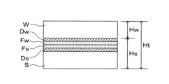
本実施形態にかかる後述のウェハ処理システム1では、図1に示すように第1基板としての上ウェハWと、第2基板としての下ウェハSとが接合された、重合基板としての重合ウェハTに対して処理を行う。そしてウェハ処理システム1では、上ウェハWを薄化する。以下、上ウェハWにおいて、下ウェハSに接合される側の面を表面Waといい、表面Waと反対側の面を裏面Wbという。同様に、下ウェハSにおいて、上ウェハWに接合される側の面を表面Saといい、表面Saと反対側の面を裏面Sbという。In the
上ウェハWは、例えばシリコン基板等の半導体ウェハであって、表面Waに複数のデバイスを含むデバイス層Dwが形成されている。また、デバイス層Dwにはさらに表面膜Fwが形成され、当該表面膜Fwを介して下ウェハSと接合されている。表面膜Fwとしては、例えば酸化膜(SiO2膜、TEOS膜)、SiC膜、SiCN膜又は接着剤などが挙げられる。 The upper wafer W is a semiconductor wafer such as a silicon substrate, and has a device layer Dw including a plurality of devices formed on its surface Wa. A surface film Fw is further formed on the device layer Dw, and the upper wafer W is bonded to the lower wafer S via the surface film Fw. Examples of the surface film Fw include an oxide film ( SiO2 film, TEOS film), a SiC film, a SiCN film, or an adhesive.
下ウェハSは、例えば上ウェハWと同様の構成を有しており、表面Saにはデバイス層Ds及び表面膜Fsが形成されている。なお、下ウェハSはデバイス層Dsが形成されたデバイスウェハである必要はなく、例えば上ウェハWを支持する支持ウェハであってもよい。かかる場合、下ウェハSは上ウェハWのデバイス層Dwを保護する保護材として機能する。The lower wafer S has, for example, the same configuration as the upper wafer W, and a device layer Ds and a surface film Fs are formed on the surface Sa. Note that the lower wafer S does not have to be a device wafer on which a device layer Ds is formed, and may be, for example, a support wafer that supports the upper wafer W. In such a case, the lower wafer S functions as a protective material that protects the device layer Dw of the upper wafer W.
なお、以降の説明で用いられる図面においては、図示の煩雑さを回避するため、デバイス層Dw、Ds及び表面膜Fw、Fsの図示を省略する場合がある。In the drawings used in the following explanation, the device layers Dw, Ds and surface films Fw, Fs may be omitted in order to avoid complexity of the illustration.
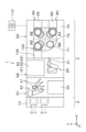
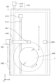
図2及び図3に示すようにウェハ処理システム1は、搬入出ステーション2と処理ステーション3を一体に接続した構成を有している。搬入出ステーション2は、例えば外部との間で複数の重合ウェハTを収容可能なカセットCが搬入出される。処理ステーション3は、重合ウェハTに対して所望の処理を施す各種処理装置を備えている。As shown in Figures 2 and 3, the
搬入出領域としての搬入出ステーション2には、カセット載置台10が設けられている。図示の例では、カセット載置台10には、複数、例えば2つのカセットCをY軸方向に一列に載置自在になっている。なお、カセット載置台10に載置されるカセットCの個数は、本実施形態に限定されず、任意に決定することができる。The loading/
処理ステーション3には、例えば3つの処理ブロックG1~G3が設けられている。第1処理ブロックG1、第2処理ブロックG2及び第3処理ブロックG3は、X軸負方向側(搬入出ステーション2側)から正方向側にこの順で並べて配置されている。それぞれの処理ブロックG1~G3間は隔壁により空間的に遮断されており、重合ウェハTは、各種処理装置に形成された搬入出口を介して、それぞれの処理ブロックG1~G3の間を搬送される。なお、各種処理装置に形成された搬入出口には、当該搬入出口の開閉を行うシャッタ(図示せず)が設けられている。The
第1処理ブロックG1には、エッチング処理装置30及びウェハ搬送装置40が設けられている。エッチング処理装置30は、例えば鉛直方向に2段に積層して設けられている。ウェハ搬送装置40は、エッチング処理装置30のY軸正方向側に配置されている。なお、エッチング処理装置30及びウェハ搬送装置40の数や配置はこれに限定されない。The first processing block G1 is provided with an
エッチング処理装置30は、研削後の上ウェハWの裏面Wb及び下ウェハSの裏面Sbをエッチングする。この際、パーティクル除去や金属成分除去などの洗浄処理も行われる。例えば裏面Wb、Sbに対してエッチング液を供給し、当該裏面Wbをウェットエッチングする。エッチング液には、例えばFPM、HF、HNO3、H3PO4、TMAH、Choline、KOHなどが用いられる。
The
第1基板搬送装置としてのウェハ搬送装置40は、重合ウェハTを保持して搬送する、例えば2つの搬送アーム41を有している。各搬送アーム41は、水平方向、鉛直方向、水平軸回り及び鉛直軸回りに移動自在に構成されている。そして、ウェハ搬送装置40は、カセット載置台10のカセットC、エッチング処理装置30、後述する第1洗浄装置50、後述する第2洗浄装置51、後述する第1厚み測定装置52及び後述する第2厚み測定装置53に対して、重合ウェハTを搬送可能に構成されている。The
また、第1処理ブロックG1には図示しないファンフィルターユニット(FFU)が設けられている。これにより、第1処理ブロックG1の内部の清浄度が高く保たれるとともに、内部の圧力が第2処理ブロックG2と比較して高く保たれている。The first processing block G1 is also provided with a fan filter unit (FFU) (not shown). This keeps the interior of the first processing block G1 highly clean and maintains the internal pressure higher than that of the second processing block G2.
処理領域としての第2処理ブロックG2には、第1洗浄装置50、第2洗浄装置51、第1厚み測定装置52、第2厚み測定装置53及びウェハ搬送装置60が設けられている。第1洗浄装置50、第2洗浄装置51、第1厚み測定装置52及び第2厚み測定装置53は、上方からこの順で積層して設けられている。ウェハ搬送装置60は、第1洗浄装置50、第2洗浄装置51、第1厚み測定装置52及び第2厚み測定装置53のY軸負方向側に配置されている。なお、第1洗浄装置50、第2洗浄装置51、第1厚み測定装置52、第2厚み測定装置53及びウェハ搬送装置60の数や配置はこれに限定されない。The second processing block G2 as a processing area is provided with a
第1洗浄装置50は、後述する加工装置70における研削前の上ウェハWの裏面Wbと下ウェハSの裏面Sbを洗浄する。例えば裏面Wbに洗浄液を供給して当該裏面Wbをスピン洗浄し、裏面Sbにブラシを当接させて当該裏面Sbをスクラブ洗浄する。The
第2洗浄装置51は、後述する加工装置70における研削後の上ウェハWの裏面Wbと下ウェハSの裏面Sbを洗浄する。第2洗浄装置51も、第1洗浄装置50と同様に、例えば裏面Wbに洗浄液を供給して当該裏面Wbをスピン洗浄し、裏面Sbにブラシを当接させて当該裏面Sbをスクラブ洗浄する。The
第1厚み測定装置52は、後述する加工装置70における研削前の上ウェハWの厚みHw(図4を参照)、及び当該上ウェハWを含む重合ウェハTの全体厚みHt(図4を参照)を測定する。また、第1厚み測定装置52は、研削前の重合ウェハTの水平方向の向き及び位置を調節する。なお、第1厚み測定装置52の詳細な構成、及び厚み測定の詳細な方法については後述する。The first
第2厚み測定装置53は、後述する加工装置70における研削後の上ウェハWの厚みHw(図4を参照)を測定する。また、第2厚み測定装置53は、研削後の重合ウェハTの水平方向の向き及び位置を調節する。なお、第2厚み測定装置53の詳細な構成、及び厚み測定の詳細な方法については後述する。The second
第2基板搬送装置としてのウェハ搬送装置60は、重合ウェハTを吸着保持面(図示せず)により吸着保持して搬送する、例えば2つの搬送アーム61を有している。各搬送アーム61は、水平方向、鉛直方向、水平軸回り及び鉛直軸回りに移動自在に構成されている。そして、ウェハ搬送装置60は、第2洗浄装置51、第1厚み測定装置52及び後述する加工装置70に対して、重合ウェハTを搬送可能に構成されている。The
なお、本実施形態においては、後述のウェハ処理の工程に基づいて、ウェハ搬送装置60による第1洗浄装置50及び第2厚み測定装置53に対する重合ウェハTの搬送が行われない場合を例に説明を行うが、ウェハ処理の工程に応じて、第1洗浄装置50及び第2厚み測定装置53に対して重合ウェハTが搬送可能に構成されていてもよい。In this embodiment, an example will be described in which the
加工領域としての第3処理ブロックG3には、加工装置70が1つ設けられている。なお、加工装置70の数や配置はこれに限定されない。The third processing block G3, which serves as the processing area, is provided with one
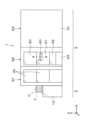
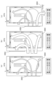
加工装置70は、回転テーブル71を有している。回転テーブル71上には、重合ウェハTを吸着保持する、第3基板保持部としてのチャック72が4つ設けられている。チャック72には例えばポーラスチャックが用いられ、重合ウェハTのうち下ウェハSの裏面Sbを吸着保持する。チャック72の表面、すなわち重合ウェハTの保持面は、側面視において中央部が端部に比べて突出した凸形状を有している。なお、この中央部の突出は微小であるため、以下の説明の図示においては、チャック72の凸形状を省略している。The
図5に示すように、チャック72はチャックベース73に保持されている。チャックベース73には、後述する各研削ユニット(粗研削ユニット80、中研削ユニット90及び仕上研削ユニット100)が備える研削ホイールとチャック72の相対的な傾きを調整する傾き調整部74が設けられている。傾き調整部74は、チャックベース73の下面に設けられた固定軸75と複数、例えば2本の昇降軸76を有している。各昇降軸76は伸縮自在に構成され、チャックベース73を昇降させる。この傾き調整部74によって、チャックベース73の外周部の一端部(固定軸75に対応する位置)を基点に、他端部を昇降軸76によって鉛直方向に昇降させることで、チャック72及びチャックベース73を傾斜させることができる。そしてこれにより、加工位置A1~A3の各研削ユニット80、90、100が備える研削ホイールの表面とチャック72の表面との相対的な傾きを調整することができる。As shown in FIG. 5, the
なお、傾き調整部74の構成はこれに限定されず、研削ホイールの表面に対するチャック72の表面の相対的な角度(平行度)を調整することができれば、任意に選択できる。The configuration of the
図2に示すように4つのチャック72は、回転テーブル71が回転することにより、受渡位置A0及び加工位置A1~A3に移動可能になっている。また、4つのチャック72はそれぞれ、回転機構(図示せず)によって鉛直軸回りに回転可能に構成されている。2, the four
受渡位置A0では、ウェハ搬送装置60による重合ウェハTの受け渡しが行われる。加工位置A1には粗研削ユニット80が配置され、上ウェハWを粗研削する。加工位置A2には中研削ユニット90が配置され、上ウェハWを中研削する。加工位置A3には仕上研削ユニット100が配置され、上ウェハWを仕上研削する。At the transfer position A0, the overlapped wafer T is transferred by the
図5に示すように、粗研削ユニット80は、下面に環状の粗研削砥石を備える粗研削ホイール81、当該粗研削ホイール81を支持するマウント82、当該マウント82を介して粗研削ホイール81を回転させるスピンドル83、及び、例えばモータ(図示せず)を内蔵する駆動部84を有している。また粗研削ユニット80は、図2に示す支柱85に沿って鉛直方向に移動可能に構成されている。5, the
中研削ユニット90は粗研削ユニット80と同様の構成を有している。すなわち中研削ユニット90は、環状の中研削砥石を備える中研削ホイール91、マウント92、スピンドル93、駆動部94、及び支柱95を有している。中研削砥石の砥粒の粒度は、粗研削砥石の砥粒の粒度より小さい。The
仕上研削ユニット100は粗研削ユニット80及び中研削ユニット90と同様の構成を有している。すなわち仕上研削ユニット100は、環状の仕上研削砥石を備える仕上研削ホイール101、マウント102、スピンドル103、駆動部104、及び支柱105を有している。仕上研削砥石の砥粒の粒度は、中研削砥石の砥粒の粒度より小さい。The
また、第3処理ブロックG3には図示しない排気ユニットが設けられている。これにより、加工装置70における研削処理により発生するパーティクル等の排出が行われるとともに、当該第3処理ブロックG3の内部圧力が第2処理ブロックG2との内部圧力と比較して低く保たれている。すなわちウェハ処理システム1においては、第1処理ブロックG1、第2処理ブロックG2、第3処理ブロックG3の内部圧力が、それぞれこの順に高くなるように制御されている。In addition, the third processing block G3 is provided with an exhaust unit (not shown). This allows particles and the like generated by the grinding process in the
図2に示すように、以上のウェハ処理システム1には、制御装置110が設けられている。制御装置110は、例えばCPUやメモリ等を備えたコンピュータであり、プログラム格納部(図示せず)を有している。プログラム格納部には、ウェハ処理システム1におけるウェハ処理を制御するプログラムが格納されている。なお、上記プログラムは、コンピュータに読み取り可能な記憶媒体Hに記録されていたものであって、当該記憶媒体Hから制御装置110にインストールされたものであってもよい。As shown in FIG. 2, the
次に、上述した第1厚み測定装置52の詳細な構成について説明する。Next, the detailed configuration of the first
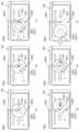
図6及び図7に示すように、第1厚み測定装置52は、重合ウェハTを保持する、第1基板保持部としてのチャック300を有している。チャック300は、重合ウェハTのうち下ウェハSの裏面Sbの中央部を吸着保持する。なお、チャック300の径は、例えば重合ウェハTの径の半分以下である。6 and 7, the first
チャック300には、チャック300の中心部から外端部まで径方向(Y軸方向)に延伸する切り欠き部301が形成されている。切り欠き部301は、後述する全体厚み測定部330の下センサ332が進退可能に形成されている。The
チャック300は、鉛直軸回りに回転自在であるとともに、水平方向に移動自在に構成されている。チャック300の下方には、当該チャック300を回転させる回転機構310が設けられている。回転機構310には、例えばモータなどの駆動部(図示せず)が内蔵されている。回転機構310は、支持部材311に支持されている。支持部材311は、水平方向(Y軸方向)に延伸するレール312に取り付けられている。支持部材311は、レール312に設けられた移動機構313により、当該レール312に沿って移動自在に構成されている。移動機構313には、例えばモータなどの駆動部(図示せず)が内蔵されている。なお、本実施形態においては、チャック300を駆動させる回転機構310及び移動機構313が、本開示の技術にかかる「第1駆動部」を構成する。The
チャック300の側方(X軸正方向側)には、第1位置検出部としての位置検出部320が設けられている。位置検出部320は、研削前の重合ウェハTの水平方向位置を検出する。位置検出部320は、チャック300に保持された下ウェハSの外周に光を照射し、さらにその光を受光するセンサを有している。あるいは位置検出部320は、下ウェハSの外周を撮像するセンサを有していてもよい。そして、チャック300に保持された重合ウェハTを回転させながら、位置検出部320で下ウェハSのノッチ部の位置を検出し、さらに重合ウェハT(上ウェハW)の中心部の位置(偏心量)を検出する。位置検出部320の検出結果は、制御装置110に出力される。そして、この検出結果に基づいて、重合ウェハTの水平方向の向きを調節し(θアライメント)、水平方向の位置を調節する(X-Yアライメント)。なお、本実施形態では下ウェハSのノッチ部の位置を検出したが、これに限定されない。例えば、下ウェハSのオリフラの位置を検出して、重合ウェハTの水平方向の向き及び位置を調節してもよい。
A
チャック300の上方及び下方には、全体厚み測定部330が設けられている。全体厚み測定部330は、図4に示す重合ウェハTの全体厚みHtを測定する。なお、全体厚み測定部330で測定された重合ウェハTの全体厚みHtは、制御装置110に出力される。An overall
図6~図8に示すように全体厚み測定部330は、上センサ331、下センサ332及び図示しない算出部を有している。上センサ331は、チャック300に保持された重合ウェハTの上方に配置され、上センサ331から上ウェハWの裏面Wbまでの距離を測定する。下センサ332は、チャック300に保持された重合ウェハTの下方に配置され、下センサ332から下ウェハSの裏面Sbまでの距離を測定する。また、上センサ331と下センサ332は同じ座標軸上に対向して配置され、上センサ331の測定点と下センサ332の測定点は平面視において同じ位置になる。そして、全体厚み測定部330では、上センサ331と上ウェハWの裏面Wb間の距離と、下センサ332と下ウェハSの裏面Sb間の距離とに基づいて、算出部により重合ウェハTの全体厚みHtを導出する。なお、上センサ331と下センサ332には、距離を測定するものであれば公知のセンサを使用することができるが、例えば共焦点センサが用いられる。また、図示しない算出部は、第1厚み測定装置52の内部に設けられていてもよいし、第1厚み測定装置52の外部に設けられていてもよい。As shown in FIGS. 6 to 8, the total
上センサ331と下センサ332はそれぞれ、チャック300が水平方向に移動することで、当該チャック300に対して相対的に移動する。また、下センサ332は、切り欠き部301に対して相対的に進退自在に構成されている。すなわち、チャック300が水平方向に移動することで、下センサ332は、切り欠き部301に対して進入し、又は退避する。そして、全体厚み測定部330は、重合ウェハTの全体厚みHtを複数点で測定することができる。The
なお、上センサ331及び下センサ332は、前述の位置検出部320による水平方向位置の検出において重合ウェハTを回転させた際に、下センサ332と切り欠き部301が干渉しない位置、すなわち位置検出部320よりもY軸正方向側に配置される。
The
チャック300の上方には、第1測定部としての部分厚み測定部340が更に設けられている。部分厚み測定部340は、図4に示す上ウェハWの厚みHwを測定する。部分厚み測定部340は、上ウェハWに接触せずに当該上ウェハWの厚みを測定する。なお、部分厚み測定部340で測定された上ウェハWの厚みHwは、制御装置110に出力される。制御装置110では、全体厚み測定部330で測定された重合ウェハTの全体厚みHtから上ウェハWの厚みHwを差し引いた、上ウェハW以外の厚みHsを算出する。この厚みHsは、下ウェハSの厚み、デバイス層Dw、Dsの厚み、及び表面膜Fw、Fsの厚みを含むものであるが、以下の説明では簡略化して、下ウェハSの厚みHsという場合がある。Above the
算出された下ウェハSの厚みHsは、制御装置110に出力される。そして、かかる下ウェハSの厚みHsに基づいて、加工装置70における研削ホイールの表面に対するチャック72の表面の相対的な角度(平行度)を調整する。The calculated thickness Hs of the lower wafer S is output to the
図6~図8に示すように部分厚み測定部340は、センサ341と図示しない算出部を有している。センサ341は、上ウェハWに対して光を照射し、さらに上ウェハWの表面Waから反射した反射光と、裏面Wbから反射した反射光とを受光する。そして、部分厚み測定部340では、両反射光に基づいて、算出部により上ウェハWの厚みHwを測定する。またセンサ341は、Y軸方向において前述の位置検出部320と同じ位置に配置されている。なお、センサ341には、厚みを測定するものであれば公知のセンサを使用することができるが、例えば分光干渉式センサが用いられる。また、図示しない算出部は、第1厚み測定装置52の内部に設けられていてもよいし、第1厚み測定装置52の外部に設けられていてもよい。6 to 8, the partial
センサ341は、チャック300が水平方向に移動することで、当該チャック300に対して相対的に移動する。そして、部分厚み測定部340は、上ウェハWの厚みHwを複数点で測定することができる。The
全体厚み測定部330及び部分厚み測定部340は、それぞれ平面視における同一の測定点において、重合ウェハTの全体厚みHt及び上ウェハWの厚みHwを測定する。すなわち、図9に示すように全体厚み測定部330及び部分厚み測定部340は、それぞれ、重合ウェハTの全体厚みHt及び上ウェハWの厚みHwを例えば径方向に3点で測定する。測定点P1は上ウェハWの中心部である。測定点P2は上ウェハWの中間部であり、上ウェハWの半径をRとした場合の、中心部からR/2の位置である。測定点P3は上ウェハWの外周部である。The total
図10(a)に示すように、全体厚み測定部330による測定点P1での全体厚みHtの測定に際しては、チャック300(重合ウェハT)の回転を停止した状態で、重合ウェハTの全体厚みHtを測定する。この際、下センサ332は、切り欠き部301に進入している。したがって、下センサ332とチャック300の干渉を回避するため、チャック300を回転させない。
一方、図11(a)に示すように、部分厚み測定部340による測定点P1での上ウェハWの厚みHwの測定に際しては、センサ341とチャック300の干渉が生じないため、チャック300(重合ウェハT)は回転させてもよいし、回転を停止させてもよい。
10A, when the total
On the other hand, as shown in FIG. 11A, when the partial
図10(b)に示すように、全体厚み測定部330による測定点P2での全体厚みHtの測定に際しては、チャック300を回転させながら、重合ウェハTの全体厚みHtを周方向に複数点で測定する。この際、チャック300の径が重合ウェハTの径の半分以下であって、下センサ332は切り欠き部301から退避しているので、チャック300を回転させても、下センサ332とチャック300が干渉することはない。
また、図11(b)に示すように、部分厚み測定部340による測定点P2での上ウェハWの厚みHwの測定に際しても、チャック300を回転させながら、上ウェハWの厚みHwを周方向に複数点で測定する。
そして、測定点P2において、測定された周方向の複数点の移動平均値を算出し、当該測定点P2における重合ウェハTの全体厚みHt、又は上ウェハWの厚みHwとする。なお、測定点P2における測定厚みは、周方向の複数点の移動中央値としてもよい。
10B, when measuring the total thickness Ht at measurement point P2 by total
Also, as shown in FIG. 11B, when the partial
Then, at the measurement point P2, a moving average value of the measured multiple points in the circumferential direction is calculated and set as the total thickness Ht of the laminated wafer T or the thickness Hw of the upper wafer W at the measurement point P2. The measured thickness at the measurement point P2 may be a moving median value of the measured multiple points in the circumferential direction.
図10(c)及び図11(c)のそれぞれに示すように、測定点P3においても、測定点P2と同様に重合ウェハTの全体厚みHt及び上ウェハWの厚みHwを測定する。As shown in Figures 10 (c) and 11 (c), the total thickness Ht of the overlapping wafer T and the thickness Hw of the upper wafer W are measured at measurement point P3, as at measurement point P2.
なお、本実施形態では測定点P2、P3において、周方向の複数点の移動平均値又は移動中央値を測定点P2、P3における測定厚みとしたが、例えば指定座標において厚み測定を行ってもよい。例えば測定点P2、P3において、重合ウェハTの回転を停止した状態で、重合ウェハTの全体厚みHt、又は上ウェハWの厚みHwを測定する。そうすると、測定点P2、P3において、周方向に1点の全体厚みHt又は上ウェハWの厚みHwが測定される。そして、かかる指定座標において測定された厚みを、代表点として測定点P2、P3の厚みとして用いてもよい。In this embodiment, the moving average or moving median of multiple points in the circumferential direction is used as the measured thickness at measurement points P2 and P3, but thickness measurement may also be performed at specified coordinates, for example. For example, at measurement points P2 and P3, the total thickness Ht of the overlapped wafer T or the thickness Hw of the upper wafer W is measured with the rotation of the overlapped wafer T stopped. Then, at measurement points P2 and P3, the total thickness Ht or the thickness Hw of the upper wafer W is measured at one point in the circumferential direction. The thickness measured at such specified coordinates may then be used as the thickness at measurement points P2 and P3 as a representative point.
また、本実施形態では、上ウェハWの厚みHwの測定結果は、後述するようにチャック72の表面と仕上研削ホイール101の表面の平行度を調整するために用いられるが、その用途はこれに限定されない。例えば、上ウェハWの厚みHwの傾向を把握するために、指定した測定点で上ウェハWの厚みHwを測定してもよい。In this embodiment, the measurement result of the thickness Hw of the upper wafer W is used to adjust the parallelism between the surface of the
なお、本実施形態の第1厚み測定装置52では、チャック300が水平方向(Y軸方向)に移動し、全体厚み測定部330の上センサ331と下センサ332、部分厚み測定部340のセンサ341が固定されていたが、チャック300と全体厚み測定部330又は部分厚み測定部340が相対的に水平方向に移動すればよい。例えば、チャック300が固定され、上センサ331と下センサ332、又はセンサ341が水平方向に移動してもよい。あるいは、チャック300が水平方向に移動し、さらに上センサ331と下センサ332、又はセンサ341も水平方向に移動してもよい。In the first
図6に示すように、第1厚み測定装置52のX軸負方向側の側壁面には、第1シャッタ350が設けられている。第1シャッタ350は駆動機構351により第1搬送口を開閉自在に構成されている。そして、この第1シャッタ350が開放されることにより、第1厚み測定装置52と第1処理ブロックG1の内部が連通し、ウェハ搬送装置40による重合ウェハTの搬入出が行われる。6, a
また、第1厚み測定装置52のY軸負方向側の側壁面には、第2シャッタ360が設けられている。第2シャッタ360は駆動機構361により第2搬送口を開閉自在に構成されている。そして、この第2シャッタ360が開放されることにより、第1厚み測定装置52と第2処理ブロックG2の内部が連通し、ウェハ搬送装置60による重合ウェハTの搬入出が行われる。A
第1厚み測定装置52の下部には、排気部370が接続されている。排気部370は、レール312等の駆動部分の下方に設けられた排気経路371と、当該排気経路371に接続される真空ポンプ等の排気機構372を有している。排気部370は、排気機構372の動作により、例えばチャック300の回転や移動等の駆動により生じるパーティクル等を第1厚み測定装置52の外部に排出する。An
また排気部370は、第1厚み測定装置52の処理空間を排気(減圧)可能に構成されている。第1厚み測定装置52の内部圧力は、第1処理ブロックG1の内部圧力よりも低く、且つ、第2処理ブロックG2の内部圧力よりも高い圧力で保たれるように制御される。換言すれば、第1厚み測定装置52においては、第1シャッタ350の開放時において第1処理ブロックG1から気流が流入し、第2シャッタ360の開放時において第2処理ブロックG2へ気流が流出する。これにより、図12に示すように、第1厚み測定装置52の内部に加工装置70における研削処理により生じたパーティクル等が流入することが抑制されるとともに、清浄空間である第1処理ブロックG1(カセットC)側にパーティクル等が流出することが抑制される。
The
具体的には、例えば図12(a)に示すように第1シャッタ350及び第2シャッタ360の閉塞時においては、第1厚み測定装置52からの気流の流出は起きておらず、排気部370からのみ気流が排出される。なお、このように第1シャッタ350が閉塞されている場合であっても、図12(a)に示したように、当該第1シャッタ350側に形成された微小隙間から、清浄空間である第1処理ブロックG1からの微量の気流が流入している。
また、図12(b)に示すように、第1シャッタ350を開放した場合、排気部370からのみ気流が排出される。
更に、図12(c)に示すように、第2シャッタ360を開放した場合、当該第2シャッタ360側から第1厚み測定装置52への気流の流入は発生せず、また、第1シャッタ350側から第1厚み測定装置52の外部への気流の流出も発生しない。
Specifically, for example, as shown in Fig. 12(a), when the
Furthermore, as shown in FIG. 12B , when the
Furthermore, as shown in Figure 12 (c), when the
このように、第1厚み測定装置52には、第1シャッタ350(第1処理ブロックG1)側からのみ気流が流入し、第2シャッタ360(加工装置70)側からの気流は流入しない。すなわち、加工装置70からのパーティクル等の流入が抑制される。
また、第1厚み測定装置52からは、第2シャッタ360(加工装置70)側及び排気部370のみから気流が流出し、第1シャッタ350(第1処理ブロックG1)側へは気流が流出しない。すなわち、清浄空間である第1処理ブロックG1にパーティクル等が流出することが抑制される。
また更に、図12に示したように第1厚み測定装置52においては、第1シャッタ350と第2シャッタ360とが同時に開放されるタイミングを作らない。これにより、加工装置70から第1処理ブロックG1にパーティクル等が流出することが更に抑制される。
In this way, airflow flows into the first
Moreover, from the first
12, in the first
次に、第2厚み測定装置53の詳細な構成について説明する。なお、第2厚み測定装置53において、第1厚み測定装置52と実質的に同一の機能構成を有する要素については、同一の符号を付することにより重複説明を省略する。Next, we will explain the detailed configuration of the second
図13及び図14に示すように、第2厚み測定装置53は、重合ウェハTを保持する、第2基板保持部としてのチャック400を有している。チャック400は、重合ウェハTのうち下ウェハSの裏面Sbの中央部を吸着保持する。なお、チャック400の径は、例えば第1厚み測定装置52が備えるチャック300の径よりも大きく、重合ウェハTの径の半分以上であってもよい。13 and 14, the second
第2厚み測定装置53においては研削後の上ウェハWの厚みHw、換言すれば、第1厚み測定装置52における研削前の上ウェハWの厚みHwよりも小さい厚みHwの測定が行われる。そこで、このようにチャック300よりも大径のチャック400で重合ウェハTを吸着保持することで、研削により薄化された重合ウェハTに反りが生じることが抑制される。The second
チャック400は、回転機構310により鉛直軸回りに回転自在であるとともに、レール312に沿って水平方向に移動自在に構成されている。また、チャック400の側方(X軸正方向側)には、第2位置検出部としての位置検出部320が設けられており、研削後の重合ウェハTの水平方向の向き及び位置を調節するとともに、上ウェハWの中心部の位置(偏心量)を検出する。なお、本実施形態においては、チャック400を駆動させる回転機構310及び移動機構313が、本開示の技術にかかる「第2駆動部」を構成する。
The
チャック400の上方には、研削後の上ウェハWの厚みHwを測定する、第2測定部としての部分厚み測定部440が設けられている。部分厚み測定部440は、上ウェハWに接触せずに当該上ウェハWの厚みを測定する。なお、上述のように第2厚み測定装置53においては研削後の上ウェハWの厚みHw、換言すれば、第1厚み測定装置52における研削前の上ウェハWの厚みHwよりも小さい厚みHwの測定が行われる。このため、部分厚み測定部440には、第1厚み測定装置52が備える部分厚み測定部340よりも小さな厚みを測定することが可能なセンサ441が設けられる。Above the
なお、部分厚み測定部440で測定された上ウェハWの厚みHwは、制御装置110に出力される。そして、かかる上ウェハWの厚みHwに基づいて、ウェハ処理システム1において次に処理される重合ウェハTの研削処理に際しての、研削ホイールの表面に対するチャック72の表面の相対的な角度(平行度)を調整する。The thickness Hw of the upper wafer W measured by the partial
部分厚み測定部440は、平面視において、第1厚み測定装置52における全体厚み測定部330及び部分厚み測定部340と同一の測定点において上ウェハWの厚みHwを測定する。すなわち、部分厚み測定部440は、上ウェハWの厚みHwを例えば図9に示した径方向の3点で測定する。なお、部分厚み測定部440による上ウェハWの厚みHwの測定方法は、図11に示した部分厚み測定部340による上ウェハWの厚みHwの測定方法と同様である。The partial
なお、第2厚み測定装置53においても、第1厚み測定装置52と同様に、測定点P2、P3における厚み測定に際して、周方向の複数点の移動平均値又は移動中央値を算出することに代え、指定座標において測定された厚みを代表点として、測定点P2、P3の厚みとして用いてもよい。In addition, in the second
また、本実施形態では、上ウェハWの厚みHwの測定結果は、次に処理される重合ウェハTの研削処理に際しての、研削ホイールの表面に対するチャック72の表面の相対的な角度を調整するために用いられるが、その用途はこれに限定されない。例えば、上ウェハWの厚みHwの傾向を把握するために、指定した測定点で上ウェハWの厚みHwを測定してもよい。In this embodiment, the measurement result of the thickness Hw of the upper wafer W is used to adjust the relative angle of the surface of the
なお、上述したように第2厚み測定装置53においては重合ウェハTの全体厚みHtの測定は行われない。このため、第2厚み測定装置53には、第1厚み測定装置52のように全体厚み測定部330が設けられていない。また、このように第2厚み測定装置53には全体厚み測定部330(下センサ332)が設けられていないため、チャック400には、下センサ332を進入させるための切欠き部は形成されていない。As described above, the second
図13に示すように、第2厚み測定装置53のX軸負方向側の側壁面には、第1シャッタ350が設けられている。第1シャッタ350は駆動機構351により第1搬送口を開閉自在に構成されている。そして、この第1シャッタ350が開放されることにより、第2厚み測定装置53と第1処理ブロックG1の内部が連通し、ウェハ搬送装置40による重合ウェハTの搬入出が行われる。13, a
なお、上述したように第2厚み測定装置53においては、第2処理ブロックG2のウェハ搬送装置60による重合ウェハTの搬入出が行われず、第1処理ブロックG1のウェハ搬送装置40のみにより重合ウェハTの搬入出が行われる。このため、第2厚み測定装置53には、第2処理ブロックG2側の第2搬送口が形成されておらず、すなわち第2シャッタ360が設けられていない。上述したように第2厚み測定装置53においては研削後の重合ウェハT(上ウェハW)の厚みHwが測定されるが、このように第2処理ブロックG2側の第2シャッタ360を省略し、ウェハ搬送装置40のみにより重合ウェハTの搬入出を行うことで、第2厚み測定装置53の内部に加工装置70における研削処理により生じたパーティクル等が流入することを防止する。As described above, in the second
また、第2厚み測定装置53の下部には排気部370が設けられている。これにより、例えばチャック400の回転や水平方向への移動等により生じるパーティクル等を第2厚み測定装置53の外部に排出可能に構成されるとともに、第2厚み測定装置53の内部圧力を減圧可能に構成されている。第2厚み測定装置53の内部圧力は、例えば第1処理ブロックG1の内部圧力よりも低い圧力で保たれるように制御される。In addition, an
本実施形態にかかる第1厚み測定装置52及び第2厚み測定装置53は以上のように構成されている。次に、以上のように構成されたウェハ処理システム1を用いて行われるウェハ処理について説明する。本実施形態では、ウェハ処理システム1の外部に設けられた接合装置(図示せず)において上ウェハWと下ウェハSが接合され、予め重合ウェハTが形成されている。The first
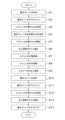
先ず、重合ウェハTを複数収納したカセットCが、搬入出ステーション2のカセット載置台10に載置される。次に、ウェハ搬送装置40によりカセットC内の重合ウェハTが取り出され、第1洗浄装置50に搬送される。第1洗浄装置50では、重合ウェハTを回転させながら上ウェハWの裏面Wbに洗浄液を供給し、当該裏面Wbをスピン洗浄する。また、洗浄ブラシ(図示せず)を下ウェハSの裏面Sbに当接させた状態で洗浄液を供給して、当該裏面Sbをスクラブ洗浄する(図15のステップE1)。First, a cassette C containing a plurality of overlapping wafers T is placed on the cassette mounting table 10 of the loading/
次に、第1厚み測定装置52の第1シャッタ350が開放され、ウェハ搬送装置40により重合ウェハTが第1厚み測定装置52に搬送される。この際、第1厚み測定装置52の内部圧力は第1処理ブロックG1の内部圧力よりも低く制御されているため、第1シャッタ350の開放により、清浄空間である第1処理ブロックG1が汚染されることが抑制される。第1厚み測定装置52では、先ず搬入出位置(ホーム位置)において、チャック300によって重合ウェハTが吸着保持される。Next, the
続いて、チャック300を図16(a)に示すようにアライメント位置に移動させる。そして、図16(b)に示すように重合ウェハTを回転させながら、位置検出部320で重合ウェハTの水平方向位置を検出し、さらに上ウェハWの中心部の位置(偏心量)を検出する。この検出結果に基づいて、重合ウェハTの水平方向の向きが調節され(θアライメント)、水平方向の位置も調節される(X-Yアライメント)(図15のステップE2)。Next, the
またアライメント位置においては、図11に示した方法により、部分厚み測定部340で研削前の上ウェハWの厚みHwを測定する(図15のステップE3)。すなわち、先ず、上ウェハWの中心部(測定点P1)での厚みHwを測定する。測定点P1での上ウェハWの厚みHwの測定に際しては、チャック300(重合ウェハT)を回転させてもよいし、回転を停止させてもよい。また、測定点P1での上ウェハWの厚みHwの測定は重合ウェハTの水平方向位置の検出(ステップE2)と同時に行われてもよい。このように測定された上ウェハWの厚みHw(厚みHwの分布)は、制御装置110に出力される。
At the alignment position, the thickness Hw of the upper wafer W before grinding is measured by the partial
次に、図16(c)に示すように、チャック300のY軸負方向側への移動及び回転を順次行い、上ウェハWの径方向の複数点(測定点P2、P3)での厚みHwを測定する。測定点P2、P3での上ウェハWの厚みHwの測定に際しては、チャック300を回転させながら上ウェハwの厚みHwを周方向に複数点で測定し、測定された周方向の複数点の移動平均値又は移動中央値を算出する。16(c), the
続いて、図16(d)に示すように、チャック300を全体厚み測定部330側に移動させ、図10に示した方法により重合ウェハTの全体厚みHtを測定する(図15のステップE4)。すなわち、先ず、重合ウェハTの中心部(測定点P1)での全体厚みHtを測定する。測定点P1においては、下センサ332が切り欠き部301に進入しているため、重合ウェハTの回転を停止した状態で、全体厚み測定部330によって測定点P1における重合ウェハTの全体厚みHtを測定する。16(d), the
次に、図16(e)に示すように、チャック300のY軸負方向側への移動及び回転を順次行い、重合ウェハTの径方向の複数点(測定点P2、P3)での全体厚みHtを測定する。測定点P2、P3での重合ウェハTの全体厚みHtの測定に際しては、チャック300を回転させながら重合ウェハTの全体厚みHtを周方向に複数点で測定し、測定された周方向の複数点の移動平均値又は移動中央値を算出する。このように測定された重合ウェハTの全体厚みHt(全体厚みHtの分布)は、制御装置110に出力される。
16( e), the
以上のようにステップE2におけるアライメントと、ステップE3、E4における厚み測定が終了すると、図16(f)に示すように、チャック300を搬入出位置に移動させる。この際、チャック300を回転させることで、ステップE2において測定された上ウェハWの水平方向位置を所望の位置に位置合わせする。After the alignment in step E2 and the thickness measurements in steps E3 and E4 are completed, the
制御装置110では、ステップE4で測定された重合ウェハTの厚みHtから、ステップE3で測定された上ウェハWの厚みHwを差し引いて、下ウェハSの厚みHsを算出する(図15のステップE5)。なお、この厚みHsは、上述したように下ウェハSの厚み、デバイス層Dw、Dsの厚み、及び表面膜Fw、Fsの厚みを含む。下ウェハSの厚みHsは各測定点P1、P2、P3において算出され、これにより下ウェハSの厚みHsの分布が得られる。The
また制御装置110では、ステップE5で算出された下ウェハSの厚みHsの分布に基づいて、加工装置70の加工位置A3における傾き調整部74を制御する。具体的には、下ウェハSの厚みHsの分布に基づいて、当該下ウェハSに接合された上ウェハWの仕上研削後の面内厚みが均一になるように、チャック72の表面と仕上研削ホイール101の表面の平行度が調整される(図15のステップE6)。以下の説明においては、このチャック72の表面と仕上研削ホイール101の表面との平行度の調整を、チルト補正という場合がある。The
次に、第1厚み測定装置52の第2シャッタ360が開放され、ウェハ搬送装置60により重合ウェハTが加工装置70に搬送され、受渡位置A0のチャック72に受け渡される。この際、第1厚み測定装置52の内部圧力は第2処理ブロックG2の内部圧力よりも高く制御されているため、加工装置70から第1厚み測定装置52にパーティクル等が進入することが抑制される。Next, the
次に、回転テーブル71を回転させて、重合ウェハTを加工位置A1に移動させる。そして、粗研削ユニット80によって、上ウェハWの裏面Wbが粗研削される(図15のステップE7)。この際、接触式の厚み測定器(図示せず)を用いて重合ウェハTの全体厚みHtを測定しながら、上ウェハWを所望の厚みに研削する。Next, the rotating table 71 is rotated to move the overlapped wafer T to the processing position A1. Then, the
次に、回転テーブル71を回転させて、重合ウェハTを加工位置A2に移動させる。そして、中研削ユニット90によって、上ウェハWの裏面Wbが中研削される(図15のステップE8)。この際、接触式の厚み測定器(図示せず)を用いて重合ウェハTの全体厚みHtを測定しながら上ウェハWを研削し、その後、非接触式の厚み測定器(図示せず)を用いて上ウェハWの厚みHwを測定しながら上ウェハWを研削する。Next, the rotating table 71 is rotated to move the overlapped wafer T to processing position A2. Then, the back surface Wb of the upper wafer W is intermediately ground by the intermediate grinding unit 90 (step E8 in FIG. 15). At this time, the upper wafer W is ground while measuring the total thickness Ht of the overlapped wafer T using a contact thickness gauge (not shown), and then the upper wafer W is ground while measuring the thickness Hw of the upper wafer W using a non-contact thickness gauge (not shown).
次に、回転テーブル71を回転させて、重合ウェハTを加工位置A3に移動させる。そして、仕上研削ユニット100によって、上ウェハWの裏面Wbが仕上研削される(図15のステップE9)。この仕上研削では、ステップE6においてチルト補正が行われた、チャック72と仕上研削ホイール101が用いられる。またこの際、非接触式の厚み測定器(図示せず)を用いて上ウェハWの厚みHwを測定しながら、上ウェハWを所望の厚みに研削する。Next, the rotating table 71 is rotated to move the overlapped wafer T to processing position A3. Then, the
次に、回転テーブル71を回転させて、重合ウェハTを受渡位置A0に移動させる。受渡位置A0では、洗浄部(図示せず)によって研削後の上ウェハWの裏面Wbを洗浄してもよい。Next, the rotating table 71 is rotated to move the overlapped wafer T to the transfer position A0. At the transfer position A0, the back surface Wb of the upper wafer W after grinding may be cleaned by a cleaning unit (not shown).
加工装置70における処理が終了した重合ウェハTは、次に、ウェハ搬送装置60により第2洗浄装置51に搬送される。第2洗浄装置51では、ステップE1と同様の洗浄が行われる。すなわち、重合ウェハTを回転させながら上ウェハWの裏面Wbに洗浄液を供給し、当該裏面Wbをスピン洗浄し、洗浄ブラシ(図示せず)を下ウェハSの裏面Sbに当接させた状態で洗浄液を供給して、当該裏面Sbをスクラブ洗浄する。(図15のステップE10)。After the processing in the
次に、第2厚み測定装置53の第1シャッタ350が開放され、ウェハ搬送装置40により重合ウェハTが第2厚み測定装置53に搬送される。この際、第2厚み測定装置53の内部圧力は第1処理ブロックG1の内部圧力よりも低く制御されているため、第1シャッタ350の開放により、清浄空間である第1処理ブロックG1が汚染されることが抑制される。第2厚み測定装置53では、先ず搬入出位置(ホーム位置)において、チャック400によって重合ウェハTが吸着保持される。Next, the
続いて、チャック400を図17(a)に示すようにアライメント位置に移動させる。そして、図17(b)に示すように重合ウェハTを回転させながら、位置検出部320で重合ウェハTの水平方向位置を検出し、さらに上ウェハWの中心部の位置(偏心量)を検出する。この検出結果に基づいて、重合ウェハTの水平方向の向きが調節され(θアライメント)、水平方向の位置も調節される(X-Yアライメント)(図15のステップE11)。Next, the
またアライメント位置においては、図11に示した方法により、部分厚み測定部440で研削後の上ウェハWの厚みHwを測定する(図15のステップE12)。すなわち、先ず、上ウェハWの中心部(測定点P1)での厚みHwを測定する。測定点P1での上ウェハWの厚みHwの測定に際しては、チャック400(重合ウェハT)を回転させてもよいし、回転を停止させてもよい。なお、測定点P1での上ウェハWの厚みHwの測定は重合ウェハTの水平方向位置の検出(ステップE11)と同時に行われてもよい。
At the alignment position, the thickness Hw of the upper wafer W after grinding is measured by the partial
次に、図17(c)に示すように、チャック400のY軸負方向側への移動及び回転を順次行い、上ウェハWの径方向の複数点(測定点P2、P3)での厚みHwを測定する。測定点P2、P3での上ウェハWの厚みHwの測定に際しては、チャック400を回転させながら上ウェハwの厚みHwを周方向に複数点で測定し、測定された周方向の複数点の移動平均値又は移動中央値を算出する。このように測定された上ウェハWの厚みHw(厚みHwの分布)は、制御装置110に出力される。17(c), the
以上のようにステップE11におけるアライメントと、ステップE12における上ウェハWの厚みHwの測定が終了すると、図17(d)に示すように、チャック400を搬入出位置に移動させる。この際、チャック400を回転させることで、ステップE11において測定された重合ウェハTの水平方向位置を所望の位置に位置合わせする。After the alignment in step E11 and the measurement of the thickness Hw of the upper wafer W in step E12 are completed as described above, the
制御装置110では、ステップE12で測定された上ウェハWの厚みHwの分布に基づいて、加工装置70の加工位置A3における傾き調整部74を制御する。具体的には、研削後の上ウェハWの厚みHwの分布に基づいて、次に処理される上ウェハWの仕上研削後の面内厚みが均一になるように、チャック72の表面と仕上研削ホイール101の表面の平行度が調整される(図15のステップE13)。すなわち、ステップE13では、n枚目(nは1以上の整数)の重合ウェハTに対してステップE1~E12を行った後、n+1枚目の重合ウェハT(上ウェハW)の研削を行うために、加工位置A3においてチャック72の表面と仕上研削ホイール101の表面の平行度を調整する。The
次に、第2厚み測定装置53の第1シャッタ350が開放され、ウェハ搬送装置40により重合ウェハTがエッチング処理装置30に搬送される。エッチング処理装置30では、上ウェハWの裏面Wb及び下ウェハSの裏面Sbに対してウェットエッチング処理(洗浄処理)が行われる(図15のステップE14)。
Next, the
その後、すべての処理が施された重合ウェハTは、ウェハ搬送装置40によりカセット載置台10のカセットCに搬送される。こうして、ウェハ処理システム1における一連のウェハ処理が終了する。After that, the laminated wafer T, which has been subjected to all the processes, is transferred by the
なお、ウェハ処理システム1では、n枚目の重合ウェハTに対する処理と、n+1枚目の重合ウェハTに対する処理が並行して行われる場合がある。かかる場合、n枚目の重合ウェハTに対してステップE1~E12を行って、ステップE13においてn+1枚目の上ウェハWの研削用のチルト補正を行う。一方、n+1枚目の重合ウェハTに対してステップE1~E5を行って、ステップE6においてn+1枚目の上ウェハWの研削用のチルト補正を行う。このようにn枚目のステップE13とn+1枚目のステップE6では、同じn+1枚目の上ウェハWの研削用のチルト補正を行う。そこで、このような場合には、ステップE12で測定したn枚目の上ウェハWの厚みHwと、ステップE5で算出したn+1枚目の下ウェハSの厚みHsとに基づいて、加工位置A3おけるチャック72の表面と仕上研削ホイール101の表面の平行度を調整する。In addition, in the
以上の実施形態によれば、加工装置70における研削前後の上ウェハWの厚みHwの測定を、加工装置70の外部に独立して設けられた第1厚み測定装置52及び第2厚み測定装置53でそれぞれ行われる。したがって、従来のように加工装置70において厚み測定を行う場合に比べて、本実施形態では加工装置70におけるウェハ処理時間を短縮することができる。その結果、ウェハ処理のスループットを向上させることができる。According to the above embodiment, the thickness Hw of the upper wafer W before and after grinding in the
また、このように第1厚み測定装置52及び第2厚み測定装置53はウェハ処理システム1において他の処理装置とは独立して設けられているため、ウェハ処理システム1における他の処理装置(例えば第1洗浄装置50や第2洗浄装置51)におけるウェハ処理時間に影響を及ぼすこともない。この結果、ウェハ処理のスループットをさらに向上させることができる。
In addition, since the first
また、本実施形態では、ステップE12で測定された上ウェハWの厚みHwに基づいて、ステップE13においてチャック72の表面と仕上研削ホイール101の表面の平行度を調整するので、次に処理される上ウェハWの仕上研削後の面内厚みを均一にすることができる。In addition, in this embodiment, the parallelism between the surface of the
また、本実施形態では、ステップE3における研削前の上ウェハWの厚みHwの測定、及びステップE4における研削前の重合ウェハTの全体厚みHtの測定を第1厚み測定装置52で行う。このように研削前の2回の厚み測定を、それぞれ同一の装置内で行うので、ウェハ処理システム1におけるウェハ処理時間をさらに短縮し、スループットをさらに向上させることができる。In addition, in this embodiment, the measurement of the thickness Hw of the upper wafer W before grinding in step E3 and the measurement of the total thickness Ht of the overlapped wafer T before grinding in step E4 are performed by the first
また、本実施形態では、ステップE5で算出した下ウェハSの厚みHsに基づいて、ステップE6においてチャック72の表面と仕上研削ホイール101の表面の平行度を調整するので、当該上ウェハWの仕上研削後の面内厚みを均一にすることができる。In addition, in this embodiment, the parallelism between the surface of the
また、本実施形態では、ステップE3における厚みHwの測定、ステップE4における全体厚みHtの測定、ステップE12における厚みHwの測定は、それぞれ同じ測定点P1、P2、P3で行われる。このため、チャック72の表面と仕上研削ホイール101の表面の平行度を適切に行うことができる。In this embodiment, the measurement of thickness Hw in step E3, the measurement of total thickness Ht in step E4, and the measurement of thickness Hw in step E12 are performed at the same measurement points P1, P2, and P3, respectively. This allows the parallelism of the surface of the
また、本実施形態では、第1厚み測定装置52及び第2厚み測定装置53において位置検出部320と部分厚み測定部340、440のセンサ341、441が、それぞれY軸方向(チャック300、400の駆動方向)において同じ位置に設けられている。これにより、位置検出部320による水平方向位置の検出と部分厚み測定部340、440による上ウェハWの中心部での厚みHwの測定を同一の位置で実施することができるため、第1厚み測定装置52及び第2厚み測定装置53におけるウェハ処理時間を短縮できる。In addition, in this embodiment, the
また、本実施形態では、ウェハ処理システム1においては第1~第3処理ブロックG1~G3の内部圧力がこの順に高く制御され、更に第1厚み測定装置52の内部圧力が第1処理ブロックG1の内部圧力よりも低く、第3処理ブロックG3の内部圧力よりも高く制御される。換言すれば、ウェハ処理システム1においては第1処理ブロックG1から第1厚み測定装置52を介して第2、第3処理ブロックG2、G3に順次流れる気流が形成される。これにより、第3処理ブロックG3の加工装置70で発生したパーティクル等が清浄空間である第1処理ブロックG1や第1厚み測定装置52の内部に流入することが抑制され、すなわち、ウェハ処理システム1における一連の処理が施された重合ウェハTが汚染されることが抑制できる。In this embodiment, the internal pressures of the first to third processing blocks G1 to G3 in the
また、本実施形態では、一連のウェハ処理において第1厚み測定装置52の第1シャッタ350と第2シャッタ360が同時に開放されるタイミングを作らない。換言すれば、重合ウェハTのアライメント、厚み測定に際して第1処理ブロックG1と第2処理ブロックG2とが直接的に連通することがないため、第1処理ブロックG1にパーティクル等が流入することを更に抑制できる。In addition, in this embodiment, the
また、本実施形態では、加工装置70における研削後の上ウェハWの厚みを測定する第2厚み測定装置53に対しては、ウェハ搬送装置60による重合ウェハTの搬送が行われず、第2シャッタ360も設けられていない。これにより、加工装置70と連通する第2処理ブロックG2と第2厚み測定装置53とが連通することがないため、一連の処理が施された重合ウェハTが汚染されることをさらに抑制できる。In addition, in this embodiment, the laminated wafer T is not transported by the
なお、以上の実施形態では図15のステップE1、ステップE10に示したように、重合ウェハTのアライメントに先立って、当該重合ウェハTの洗浄を行ったが、これら重合ウェハTの洗浄は適宜省略されてもよい。In the above embodiment, as shown in steps E1 and E10 of FIG. 15, cleaning of the laminated wafer T was performed prior to alignment of the laminated wafer T, but cleaning of the laminated wafer T may be omitted as appropriate.
また、以上の実施形態では図15のステップE11に示したように、第2厚み測定装置53において研削処理後の重合ウェハTのアライメントを行った。しかしながら、例えば研削工程(ステップE7~E9)や重合ウェハTの搬送時において当該重合ウェハTの水平方向位置にズレが生じない場合には、かかる重合ウェハTのアライメントは省略されてもよい。
In the above embodiment, as shown in step E11 of Fig. 15, alignment of the laminated wafer T after the grinding process was performed in the second
更に、以上の実施形態では図15のステップE1及びE2、ステップE10及びE11に示したように、重合ウェハTのアライメントに先立って、当該重合ウェハTの洗浄を行ったが、これら重合ウェハTの洗浄とアライメントの順序は逆であってもよい。かかる場合、重合ウェハTのアライメントは厚み測定装置の内部で行われてもよいし、又は、厚み測定装置の外部に重合ウェハTのアライメントを行うためのアライメント装置が更に設けられてもよい。Furthermore, in the above embodiments, as shown in steps E1 and E2, and steps E10 and E11 in FIG. 15, the overlapped wafer T is cleaned prior to alignment of the overlapped wafer T, but the order of cleaning and alignment of the overlapped wafer T may be reversed. In such a case, alignment of the overlapped wafer T may be performed inside the thickness measuring device, or an alignment device for aligning the overlapped wafer T may be further provided outside the thickness measuring device.
また、このように重合ウェハTの洗浄(ステップE1、E10)とアライメント(ステップE2、E11)の順序を入れ替える場合、ウェハ搬送装置60により第1洗浄装置50及び第2厚み測定装置53に対して重合ウェハTが搬送可能に構成されていてもよい。換言すれば、ウェハ搬送装置60との間で重合ウェハTの受け渡しを行うための第2シャッタ360が、第2厚み測定装置53に設けられていてもよい。
Furthermore, when the order of cleaning (steps E1, E10) and alignment (steps E2, E11) of the laminated wafer T is switched in this manner , the laminated wafer T may be configured to be transportable by the
なお、以上の実施形態では、第1厚み測定装置52と第2厚み測定装置53のそれぞれに部分厚み測定部340、440を設け、第1厚み測定装置52に全体厚み測定部330を設けて、加工位置A3におけるチルト補正に必要な情報(厚み)を収集したが、チルト補正以外に使用される情報(厚み)を収集してもよい。In the above embodiment, partial
なお、以上の実施形態では、ステップE3、E4及びE12において重合ウェハT(上ウェハW)の径方向3点(測定点P1、P2及びP3)で厚み測定を行ったが、測定点Pは4点以上であってもよい。測定点の数が多いほど、上ウェハWの厚みHwや下ウェハSの厚みHsの分布を適切に把握し、その結果、ステップE6においてチャック72の表面と仕上研削ホイール101の表面の平行度を適切に調整することができる。In the above embodiment, thickness measurements were performed at three radial points (measurement points P1, P2, and P3) of the overlapped wafer T (upper wafer W) in steps E3, E4, and E12, but the number of measurement points P may be four or more. The more measurement points there are, the more appropriately the distribution of the thickness Hw of the upper wafer W and the thickness Hs of the lower wafer S can be grasped, and as a result, the parallelism between the surface of the
また、上ウェハWの厚みHwの測定点の位置は本実施形態に限定されない。例えば研削後の上ウェハWの厚みHwに凹凸が生じる位置、すなわち特異点が予め分かっている場合には、当該特異点を厚みHwの測定点としてもよい。また例えば、ステップE12における測定点P1~P3における厚み測定後、特異点における上ウェハWの厚みHwをさらに測定してもよい。 Furthermore, the position of the measurement point for the thickness Hw of the upper wafer W is not limited to this embodiment. For example, if the position where unevenness occurs in the thickness Hw of the upper wafer W after grinding, i.e., a singular point, is known in advance, the singular point may be used as the measurement point for the thickness Hw. Also, for example, after the thickness measurement at the measurement points P1 to P3 in step E12, the thickness Hw of the upper wafer W at the singular point may be further measured.
具体的には、例えば第2厚み測定装置53において特異点での上ウェハWの厚みHwを測定する場合、チャック400に重合ウェハTが保持された状態で、チャック400(重合ウェハT)を回転させるとともに、水平方向に移動させ、部分厚み測定部440のセンサ441の直下に特異点を移動させる。これにより、上ウェハWの厚みHwを部分厚み測定部440により測定する。なお、上ウェハWの面内に複数の特異点が生じている場合には、チャック400(重合ウェハT)の回転及び移動を繰り返し行うことにより、各特異点における厚み測定を順次行うことができる。Specifically, for example, when the thickness Hw of the upper wafer W at a singular point is measured in the second
なお、このように第2厚み測定装置53において特異点での上ウェハWの厚みHwを測定する場合、当該第2厚み測定装置53の設置位置は本実施形態に限定されない。この測定はステップE14のウェットエッチング処理の後に行ってもよいため、第2厚み測定装置53は、例えば第1処理ブロックG1等に設けられていてもよい。In this manner, when the thickness Hw of the upper wafer W at the singular point is measured by the second
なお、以上の実施形態では図2及び図3に示したようにウェハ処理システム1が搬入出ステーション2と第1~第3処理ブロックG1~G3がX軸方向にこの順に並べて配置された構成を有していたが、ウェハ処理システム1の構成はこれに限られるものではない。
In the above embodiment, as shown in Figures 2 and 3, the
具体的には、図18に示す他の実施形態にかかるウェハ処理システム500のように、第1処理ブロックG1が省略されてもよい。より具体的には、ウェハ処理システム500のようにエッチング処理装置30及びウェハ搬送装置40を省略し、ウェハ処理システム500の外部で研削後の重合ウェハTにエッチング処理を施すようにしてもよい。かかる場合、第2処理ブロックG2には、カセット載置台10のカセットC、第1洗浄装置50、第2洗浄装置51、第1厚み測定装置52、第2厚み測定装置53及び加工装置70に対して、重合ウェハTを搬送可能に構成されたウェハ搬送装置510が設けられる。18 according to another embodiment, the first processing block G1 may be omitted. More specifically, the
またかかる場合、ウェハ搬送装置510は、カセットCとの間で重合ウェハTの受け渡しが可能な、例えば重合ウェハTを保持して搬送する搬送アーム41と、第1洗浄装置50、第2洗浄装置51、第1厚み測定装置52、第2厚み測定装置53及び加工装置70との間で重合ウェハTの受け渡しが可能な、重合ウェハTの吸着保持面(図示せず)を備える搬送アーム61と、を有している。In such a case, the
なお、このようにウェハ処理システム500においてはウェハ搬送装置40が省略されるため、第1洗浄装置50、第2洗浄装置51、第1厚み測定装置52及び第2厚み測定装置53にはウェハ搬送装置510のみにより重合ウェハTの搬送が行われる。換言すれば、ウェハ処理システム500においては、第1厚み測定装置52及び第2厚み測定装置53ではX軸負方向側の側面の第1シャッタ350及び駆動機構351が省略され、Y軸負方向側の側面の第2シャッタ360及び駆動機構361が設けられる。
In this manner, since the
なおウェハ搬送装置510に2本の搬送アーム61を設け、研削前の重合ウェハTを搬送するための搬送アーム61と、研削後の重合ウェハTを搬送するための搬送アーム61とを使い分けてもよい。In addition, two
今回開示された実施形態はすべての点で例示であって制限的なものではないと考えられるべきである。上記の実施形態は、添付の請求の範囲及びその主旨を逸脱することなく、様々な形態で省略、置換、変更されてもよい。The embodiments disclosed herein should be considered to be illustrative and not restrictive in all respects. The above embodiments may be omitted, substituted, or modified in various ways without departing from the scope and spirit of the appended claims.
1 ウェハ処理システム
52 第1厚み測定装置
53 第2厚み測定装置
70 加工装置
Ht 全体厚み
Hw (上ウェハの)厚み
S 下ウェハ
T 重合ウェハ
W 上ウェハ
1
Claims (18)
前記第1基板を研削する加工装置と、
前記加工装置の外部に設けられ、研削前の前記第1基板の厚みと当該第1基板を含む前記重合基板の全体厚みを測定する第1厚み測定装置と、
前記加工装置の外部に設けられ、研削後の前記第1基板の厚みを測定する第2厚み測定装置と、を備える、基板処理システム。
A substrate processing system for processing a laminated substrate in which a first substrate and a second substrate are bonded together, comprising:
a processing device that grinds the first substrate;
a first thickness measuring device provided outside the processing apparatus and configured to measure a thickness of the first substrate before grinding and a total thickness of the laminated substrate including the first substrate;
a second thickness measuring device provided outside the processing apparatus and configured to measure a thickness of the first substrate after grinding, the substrate processing system comprising:
前記重合基板を保持する第1基板保持部と、
前記第1基板保持部に保持された前記第1基板の厚みを測定する第1測定部と、
前記第1基板保持部に保持された前記重合基板の全体厚みを測定する全体厚み測定部と、を備え、
前記第1基板保持部には、当該第1基板保持部の中心部から外端部まで径方向に延伸し、前記全体厚み測定部が相対的に進退自在な切り欠き部が形成されており、
前記第2厚み測定装置は、
前記重合基板を保持する第2基板保持部と、
前記第2基板保持部に保持された前記第1基板の厚みを測定する第2測定部と、を備える、請求項1に記載の基板処理システム。 The first thickness measuring device is
a first substrate holding part for holding the laminated substrate;
a first measuring unit that measures a thickness of the first substrate held by the first substrate holding unit;
an overall thickness measuring unit that measures an overall thickness of the laminated substrate held by the first substrate holding unit,
a notch portion is formed in the first substrate holding portion, the notch portion extending radially from a center portion to an outer end portion of the first substrate holding portion and allowing the total thickness measuring portion to relatively move forward and backward;
The second thickness measuring device is
a second substrate holding part for holding the laminated substrate;
The substrate processing system according to claim 1 , further comprising: a second measuring unit configured to measure a thickness of the first substrate held by the second substrate holding unit.
前記第1基板保持部を水平方向に移動及び回転させる第1駆動部と、
前記加工装置で研削前の前記重合基板の水平方向位置を検出する第1位置検出部を備え、
前記第1位置検出部は、前記第1基板保持部の移動方向において、前記第1測定部と同じ位置に配置される、請求項2又は3に記載の基板処理システム。 The first thickness measuring device is
A first drive unit that moves and rotates the first substrate holding unit in a horizontal direction;
a first position detection unit that detects a horizontal position of the laminated substrate before grinding by the processing device;
4. The substrate processing system according to claim 2, wherein the first position detection unit is disposed at the same position as the first measurement unit in a moving direction of the first substrate holding unit.
前記第2基板保持部を水平方向に移動及び回転させる第2駆動部と、
研削後の前記重合基板の水平方向位置を検出する第2位置検出部を備え、
前記第2位置検出部は、前記第2基板保持部の移動方向において、前記第2測定部と同じ位置に配置される、請求項2~4のいずれか一項に記載の基板処理システム。 The second thickness measuring device is
A second drive unit that moves and rotates the second substrate holding unit in a horizontal direction;
a second position detection unit that detects a horizontal position of the laminated substrate after grinding;
5. The substrate processing system according to claim 2, wherein the second position detection unit is disposed at the same position as the second measurement unit in a moving direction of the second substrate holding unit.
前記加工装置に対して前記重合基板を搬送する第2基板搬送装置と、を備え、
前記第1厚み測定装置には、
前記第1基板搬送装置が進入する第1搬送口と、
前記第2基板搬送装置が進入する第2搬送口と、が形成され、
前記第2厚み測定装置には、
前記第1基板搬送装置が進入する第1搬送口が形成され、
前記第2基板搬送装置が進入する第2搬送口は形成されない、請求項1~5のいずれか一項に記載の基板処理システム。 a first substrate transfer device that transfers the laminated substrate to a cassette that can accommodate a plurality of the laminated substrates;
a second substrate transport device that transports the laminated substrate to the processing device,
The first thickness measuring device includes:
a first transfer opening through which the first substrate transfer device enters;
a second transfer opening through which the second substrate transfer device enters is formed;
The second thickness measuring device includes:
a first transfer opening through which the first substrate transfer device enters is formed;
6. The substrate processing system according to claim 1, wherein a second transfer opening through which the second substrate transfer device enters is not formed.
前記第1厚み測定装置及び前記第2厚み測定装置が設けられる処理領域と、
前記加工装置が設けられる加工領域と、が形成され、
前記搬入出領域の内部圧力を前記処理領域の内部圧力よりも高く、かつ、前記処理領域の内部圧力を前記加工領域の内部圧力よりも高く、制御する制御装置を備える、請求項1~6のいずれか一項に記載の基板処理システム。 a loading/unloading area in which a cassette capable of accommodating a plurality of the laminated substrates is placed;
a processing area in which the first thickness measurement device and the second thickness measurement device are provided;
A processing area in which the processing device is provided is formed,
The substrate processing system according to any one of claims 1 to 6, further comprising a control device that controls the internal pressure of the loading/unloading region to be higher than the internal pressure of the processing region and to be higher than the internal pressure of the processing region.
前記加工装置で研削後の前記重合基板を洗浄する第2洗浄装置と、を備え、
前記第1洗浄装置、前記第2洗浄装置、前記第1厚み測定装置及び前記第2厚み測定装置が積層して配置される、請求項1~8のいずれか一項に記載の基板処理システム。 a first cleaning device that cleans the laminated substrate before it is ground by the processing device;
a second cleaning device that cleans the laminated substrate after grinding by the processing device,
9. The substrate processing system according to claim 1, wherein the first cleaning device, the second cleaning device, the first thickness measuring device, and the second thickness measuring device are arranged in a stacked manner.
研削前の前記第1基板の厚みを第1厚み測定装置で測定することと、
研削前の前記重合基板の全体厚みを第1厚み測定装置で測定することと、
前記第1基板を加工装置で研削することと、
研削後の前記第1基板の厚みを第2厚み測定装置で測定することと、を含み、
前記第1厚み測定装置と前記第2厚み測定装置は、前記加工装置の外部に設けられている、基板処理方法。
A substrate processing method for processing a laminated substrate in which a first substrate and a second substrate are bonded together in a substrate processing system, comprising:
measuring a thickness of the first substrate before grinding with a first thickness measuring device;
measuring an overall thickness of the laminated substrate before grinding with a first thickness measuring device;
grinding the first substrate with a processing device;
measuring the thickness of the first substrate after grinding with a second thickness measuring device ;
A substrate processing method , wherein the first thickness measuring device and the second thickness measuring device are provided outside the processing device .
前記第1基板の研削に先立ち、算出された前記第2基板の厚みに基づいて、前記加工装置における第3基板保持部の前記重合基板の保持面と、研削砥石の研削面との相対的な傾きを調整することと、を含む請求項10に記載の基板処理方法。 Calculating a thickness of the second substrate based on a total thickness of the laminated substrate before grinding and a thickness of the first substrate before grinding;
11. The substrate processing method according to claim 10, further comprising: adjusting, prior to grinding the first substrate, a relative inclination between a holding surface of the laminated substrate of a third substrate holding portion in the processing apparatus and a grinding surface of a grinding wheel based on the calculated thickness of the second substrate.
次に処理される重合基板における前記第1基板の研削に先立ち、一の基板で測定された研削後の前記第1基板の厚みに基づいて、前記加工装置における第3基板保持部の前記重合基板の保持面と、研削砥石の研削面との相対的な傾きを調整する、請求項10または11に記載の基板処理方法。 In the substrate processing system, a plurality of laminated substrates are continuously processed,
12. The substrate processing method according to claim 10, further comprising the steps of: adjusting a relative inclination between a holding surface of the third substrate holding part of the processing apparatus for holding the laminated substrate and a grinding surface of a grinding wheel based on a thickness of the first substrate measured after grinding of one substrate prior to grinding of the first substrate in the laminated substrate to be processed next.
研削後の前記重合基板の水平方向位置を第2厚み測定装置で検出することと、を含む請求項10~12のいずれか一項に記載の基板処理方法。 Detecting a horizontal position of the laminated substrate before grinding with a first thickness measuring device;
13. The substrate processing method according to claim 10, further comprising: detecting a horizontal position of the laminated substrate after grinding with a second thickness measuring device.
前記第1基板の中心部における厚みの測定を、前記水平方向位置の検出と同じ位置で行う、請求項13に記載の基板処理方法。 The first thickness measuring device and the second thickness measuring device measure the thickness of the first substrate at a plurality of points in a radial direction;
The substrate processing method according to claim 13 , wherein the measurement of the thickness at the central portion of the first substrate is performed at the same position as the detection of the horizontal position.
複数の前記重合基板を収容可能なカセットに対して前記重合基板を搬送する第1基板搬送装置と、
前記加工装置に対して前記重合基板を搬送する第2基板搬送装置と、を備え、
前記第1厚み測定装置には、前記第1基板搬送装置及び前記第2基板搬送装置を進入させ、
前記第2厚み測定装置には、前記第1基板搬送装置のみを進入させて前記第2基板搬送装置は進入させない、請求項10~14のいずれか一項に記載の基板処理方法。 The substrate processing system includes:
a first substrate transfer device that transfers the laminated substrate to a cassette that can accommodate a plurality of the laminated substrates;
a second substrate transport device that transports the laminated substrate to the processing device,
The first substrate transport device and the second substrate transport device are inserted into the first thickness measuring device;
The substrate processing method according to any one of claims 10 to 14, wherein only the first substrate transport device enters the second thickness measurement device, and the second substrate transport device does not enter the second thickness measurement device.
複数の前記重合基板を収容可能なカセットが載置される搬入出領域と、
前記第1厚み測定装置及び前記第2厚み測定装置が設けられる処理領域と、
前記加工装置が設けられる加工領域と、が形成され、
前記搬入出領域の内部圧力を前記処理領域の内部圧力よりも高く、かつ、前記処理領域の内部圧力を前記加工領域の内部圧力よりも高く、制御する、請求項10~15のいずれか一項に記載の基板処理方法。 The substrate processing system includes:
a loading/unloading area in which a cassette capable of accommodating a plurality of the laminated substrates is placed;
a processing area in which the first thickness measurement device and the second thickness measurement device are provided;
A processing area in which the processing device is provided is formed,
The substrate processing method according to any one of claims 10 to 15, wherein the internal pressure of the loading/unloading region is controlled to be higher than the internal pressure of the processing region, and the internal pressure of the processing region is controlled to be higher than the internal pressure of the processing region.
前記第2厚み測定装置での前記第1基板の厚みの測定に先立って、研削後の前記重合基板を第2洗浄装置で洗浄することと、を含む、請求項10~17のいずれか一項に記載の基板処理方法。
cleaning the laminated substrate before grinding in a first cleaning device prior to measuring the thickness of the first substrate with the first thickness measuring device;
18. The substrate processing method according to claim 10, further comprising: cleaning the ground laminated substrate in a second cleaning device prior to measuring the thickness of the first substrate with the second thickness measuring device.
Applications Claiming Priority (3)
| Application Number | Priority Date | Filing Date | Title |
|---|---|---|---|
| JP2020196956 | 2020-11-27 | ||
| JP2020196956 | 2020-11-27 | ||
| PCT/JP2021/041879 WO2022113795A1 (en) | 2020-11-27 | 2021-11-15 | Substrate processing system and substrate processing method |
Publications (3)
| Publication Number | Publication Date |
|---|---|
| JPWO2022113795A1 JPWO2022113795A1 (en) | 2022-06-02 |
| JPWO2022113795A5 JPWO2022113795A5 (en) | 2023-08-08 |
| JP7581374B2 true JP7581374B2 (en) | 2024-11-12 |
Family
ID=81755980
Family Applications (1)
| Application Number | Title | Priority Date | Filing Date |
|---|---|---|---|
| JP2022565233A Active JP7581374B2 (en) | 2020-11-27 | 2021-11-15 | SUBSTRATE PROCESSING SYSTEM AND SUBSTRATE PROCESSING METHOD |
Country Status (5)
| Country | Link |
|---|---|
| US (1) | US20240017375A1 (en) |
| JP (1) | JP7581374B2 (en) |
| KR (1) | KR102928179B1 (en) |
| CN (1) | CN116529026B (en) |
| WO (1) | WO2022113795A1 (en) |
Families Citing this family (1)
| Publication number | Priority date | Publication date | Assignee | Title |
|---|---|---|---|---|
| WO2026034231A1 (en) * | 2024-08-07 | 2026-02-12 | 東京エレクトロン株式会社 | Substrate processing method and substrate processing system |
Citations (7)
| Publication number | Priority date | Publication date | Assignee | Title |
|---|---|---|---|---|
| JP2009274139A (en) | 2008-05-12 | 2009-11-26 | Ebara Corp | Method and apparatus for grinding, and control program for the apparatus |
| JP2012033585A (en) | 2010-07-29 | 2012-02-16 | Covalent Materials Corp | Polishing apparatus and polishing method |
| JP2014226749A (en) | 2013-05-22 | 2014-12-08 | 株式会社ディスコ | Grinding method |
| JP2017056523A (en) | 2015-09-17 | 2017-03-23 | 株式会社ディスコ | Grinding equipment |
| JP2017113811A (en) | 2015-12-21 | 2017-06-29 | 株式会社ディスコ | Grinding equipment |
| WO2018235619A1 (en) | 2017-06-21 | 2018-12-27 | 東京エレクトロン株式会社 | Substrate processing system, substrate processing method and computer storage medium |
| JP2021084146A (en) | 2019-11-26 | 2021-06-03 | 株式会社ディスコ | Grinding method of wafer |
Family Cites Families (12)
| Publication number | Priority date | Publication date | Assignee | Title |
|---|---|---|---|---|
| US7457680B2 (en) * | 2000-12-27 | 2008-11-25 | Tokyo Electron Limited | Conveyance method for transporting objects |
| JP2003273050A (en) * | 2002-03-15 | 2003-09-26 | Toshiba Ceramics Co Ltd | Polishing equipment |
| KR20070118617A (en) * | 2005-04-04 | 2007-12-17 | 신에쯔 한도타이 가부시키가이샤 | Manufacturing method of bonded wafer and bonded wafer and planar grinding device |
| EP1872392B1 (en) * | 2005-04-19 | 2012-02-22 | Ebara Corporation | Substrate processing apparatus |
| JP2008264913A (en) | 2007-04-18 | 2008-11-06 | Disco Abrasive Syst Ltd | Grinding equipment |
| JP2009039827A (en) * | 2007-08-09 | 2009-02-26 | Fujitsu Ltd | Polishing apparatus, substrate and method for manufacturing electronic apparatus |
| JP6051632B2 (en) * | 2011-07-20 | 2016-12-27 | 日立化成株式会社 | Abrasive and substrate polishing method |
| JP6374169B2 (en) * | 2014-01-23 | 2018-08-15 | 株式会社荏原製作所 | Polishing method and polishing apparatus |
| JP2018054500A (en) * | 2016-09-29 | 2018-04-05 | 東京エレクトロン株式会社 | Position detection system and processing device |
| JP6968201B2 (en) * | 2017-12-22 | 2021-11-17 | 東京エレクトロン株式会社 | Board processing system, board processing method and computer storage medium |
| JP7242141B2 (en) * | 2019-06-24 | 2023-03-20 | 株式会社ディスコ | Workpiece processing method |
| JP7358185B2 (en) * | 2019-10-15 | 2023-10-10 | 株式会社ディスコ | Thickness measurement device and processing equipment equipped with thickness measurement device |
-
2021
- 2021-11-15 CN CN202180077965.9A patent/CN116529026B/en active Active
- 2021-11-15 KR KR1020237021209A patent/KR102928179B1/en active Active
- 2021-11-15 JP JP2022565233A patent/JP7581374B2/en active Active
- 2021-11-15 US US18/254,608 patent/US20240017375A1/en active Pending
- 2021-11-15 WO PCT/JP2021/041879 patent/WO2022113795A1/en not_active Ceased
Patent Citations (7)
| Publication number | Priority date | Publication date | Assignee | Title |
|---|---|---|---|---|
| JP2009274139A (en) | 2008-05-12 | 2009-11-26 | Ebara Corp | Method and apparatus for grinding, and control program for the apparatus |
| JP2012033585A (en) | 2010-07-29 | 2012-02-16 | Covalent Materials Corp | Polishing apparatus and polishing method |
| JP2014226749A (en) | 2013-05-22 | 2014-12-08 | 株式会社ディスコ | Grinding method |
| JP2017056523A (en) | 2015-09-17 | 2017-03-23 | 株式会社ディスコ | Grinding equipment |
| JP2017113811A (en) | 2015-12-21 | 2017-06-29 | 株式会社ディスコ | Grinding equipment |
| WO2018235619A1 (en) | 2017-06-21 | 2018-12-27 | 東京エレクトロン株式会社 | Substrate processing system, substrate processing method and computer storage medium |
| JP2021084146A (en) | 2019-11-26 | 2021-06-03 | 株式会社ディスコ | Grinding method of wafer |
Also Published As
| Publication number | Publication date |
|---|---|
| JPWO2022113795A1 (en) | 2022-06-02 |
| WO2022113795A1 (en) | 2022-06-02 |
| CN116529026B (en) | 2025-11-25 |
| CN116529026A (en) | 2023-08-01 |
| KR20230107685A (en) | 2023-07-17 |
| KR102928179B1 (en) | 2026-02-20 |
| US20240017375A1 (en) | 2024-01-18 |
Similar Documents
| Publication | Publication Date | Title |
|---|---|---|
| JP7516528B2 (en) | Thickness measuring device and thickness measuring method | |
| TWI386989B (en) | Grinding device and grinding method | |
| JP6937370B2 (en) | Grinding equipment, grinding methods and computer storage media | |
| KR102450002B1 (en) | Substrate processing system, substrate processing method and computer storage medium | |
| JP4762647B2 (en) | Polishing apparatus and polishing method | |
| US12290898B2 (en) | Substrate processing method and substrate processing apparatus | |
| JP7018452B2 (en) | Board processing system, board processing method and computer storage medium | |
| JP6584532B2 (en) | Grinding apparatus and grinding method | |
| JP7071818B2 (en) | Board processing system | |
| JP7581374B2 (en) | SUBSTRATE PROCESSING SYSTEM AND SUBSTRATE PROCESSING METHOD | |
| JP2020110871A (en) | Substrate processing apparatus and method for identifying a region to be partially polished in a substrate processing apparatus | |
| JP2022085344A (en) | Substrate processing system and substrate processing method | |
| JP7653269B2 (en) | Processing method and processing device | |
| JP7434352B2 (en) | Substrate processing method and substrate processing apparatus | |
| JP2022046137A (en) | Substrate treatment method and substrate treatment system | |
| WO2025027806A1 (en) | Grinding device and grinding method |
Legal Events
| Date | Code | Title | Description |
|---|---|---|---|
| A521 | Request for written amendment filed |
Free format text: JAPANESE INTERMEDIATE CODE: A523 Effective date: 20230515 |
|
| A621 | Written request for application examination |
Free format text: JAPANESE INTERMEDIATE CODE: A621 Effective date: 20230515 |
|
| A131 | Notification of reasons for refusal |
Free format text: JAPANESE INTERMEDIATE CODE: A131 Effective date: 20240625 |
|
| A521 | Request for written amendment filed |
Free format text: JAPANESE INTERMEDIATE CODE: A523 Effective date: 20240820 |
|
| TRDD | Decision of grant or rejection written | ||
| A01 | Written decision to grant a patent or to grant a registration (utility model) |
Free format text: JAPANESE INTERMEDIATE CODE: A01 Effective date: 20241001 |
|
| A61 | First payment of annual fees (during grant procedure) |
Free format text: JAPANESE INTERMEDIATE CODE: A61 Effective date: 20241030 |
|
| R150 | Certificate of patent or registration of utility model |
Ref document number: 7581374 Country of ref document: JP Free format text: JAPANESE INTERMEDIATE CODE: R150 |