JP7579752B2 - クリーニングを制御する方法及びプラズマ処理装置 - Google Patents
クリーニングを制御する方法及びプラズマ処理装置 Download PDFInfo
- Publication number
- JP7579752B2 JP7579752B2 JP2021089005A JP2021089005A JP7579752B2 JP 7579752 B2 JP7579752 B2 JP 7579752B2 JP 2021089005 A JP2021089005 A JP 2021089005A JP 2021089005 A JP2021089005 A JP 2021089005A JP 7579752 B2 JP7579752 B2 JP 7579752B2
- Authority
- JP
- Japan
- Prior art keywords
- cleaning
- chamber
- substrate
- plasma
- edge ring
- Prior art date
- Legal status (The legal status is an assumption and is not a legal conclusion. Google has not performed a legal analysis and makes no representation as to the accuracy of the status listed.)
- Active
Links
- 238000004140 cleaning Methods 0.000 title claims description 76
- 238000000034 method Methods 0.000 title claims description 67
- 239000000758 substrate Substances 0.000 claims description 74
- 238000005513 bias potential Methods 0.000 claims description 37
- 239000004020 conductor Substances 0.000 claims description 23
- 239000007789 gas Substances 0.000 description 33
- 238000010586 diagram Methods 0.000 description 6
- 229910052782 aluminium Inorganic materials 0.000 description 5
- XAGFODPZIPBFFR-UHFFFAOYSA-N aluminium Chemical compound [Al] XAGFODPZIPBFFR-UHFFFAOYSA-N 0.000 description 5
- 239000011810 insulating material Substances 0.000 description 4
- 238000009792 diffusion process Methods 0.000 description 3
- 239000010453 quartz Substances 0.000 description 3
- VYPSYNLAJGMNEJ-UHFFFAOYSA-N silicon dioxide Inorganic materials O=[Si]=O VYPSYNLAJGMNEJ-UHFFFAOYSA-N 0.000 description 3
- 238000002048 anodisation reaction Methods 0.000 description 2
- 230000005684 electric field Effects 0.000 description 2
- 150000002500 ions Chemical class 0.000 description 2
- 229910052751 metal Inorganic materials 0.000 description 2
- 239000002184 metal Substances 0.000 description 2
- 238000012986 modification Methods 0.000 description 2
- 230000004048 modification Effects 0.000 description 2
- SIWVEOZUMHYXCS-UHFFFAOYSA-N oxo(oxoyttriooxy)yttrium Chemical compound O=[Y]O[Y]=O SIWVEOZUMHYXCS-UHFFFAOYSA-N 0.000 description 2
- 229910052710 silicon Inorganic materials 0.000 description 2
- 239000010703 silicon Substances 0.000 description 2
- MYMOFIZGZYHOMD-UHFFFAOYSA-N Dioxygen Chemical compound O=O MYMOFIZGZYHOMD-UHFFFAOYSA-N 0.000 description 1
- 238000007792 addition Methods 0.000 description 1
- QVGXLLKOCUKJST-UHFFFAOYSA-N atomic oxygen Chemical compound [O] QVGXLLKOCUKJST-UHFFFAOYSA-N 0.000 description 1
- 239000000919 ceramic Substances 0.000 description 1
- 239000007795 chemical reaction product Substances 0.000 description 1
- 229910001882 dioxygen Inorganic materials 0.000 description 1
- 238000009616 inductively coupled plasma Methods 0.000 description 1
- 239000000463 material Substances 0.000 description 1
- TWNQGVIAIRXVLR-UHFFFAOYSA-N oxo(oxoalumanyloxy)alumane Chemical compound O=[Al]O[Al]=O TWNQGVIAIRXVLR-UHFFFAOYSA-N 0.000 description 1
- 239000001301 oxygen Substances 0.000 description 1
- 229910052760 oxygen Inorganic materials 0.000 description 1
- 238000001020 plasma etching Methods 0.000 description 1
- HBMJWWWQQXIZIP-UHFFFAOYSA-N silicon carbide Chemical compound [Si+]#[C-] HBMJWWWQQXIZIP-UHFFFAOYSA-N 0.000 description 1
- 229910010271 silicon carbide Inorganic materials 0.000 description 1
- 238000006467 substitution reaction Methods 0.000 description 1
Images


Classifications
-
- B—PERFORMING OPERATIONS; TRANSPORTING
- B08—CLEANING
- B08B—CLEANING IN GENERAL; PREVENTION OF FOULING IN GENERAL
- B08B13/00—Accessories or details of general applicability for machines or apparatus for cleaning
-
- B—PERFORMING OPERATIONS; TRANSPORTING
- B08—CLEANING
- B08B—CLEANING IN GENERAL; PREVENTION OF FOULING IN GENERAL
- B08B7/00—Cleaning by methods not provided for in a single other subclass or a single group in this subclass
- B08B7/0035—Cleaning by methods not provided for in a single other subclass or a single group in this subclass by radiant energy, e.g. UV, laser, light beam or the like
-
- H—ELECTRICITY
- H01—ELECTRIC ELEMENTS
- H01J—ELECTRIC DISCHARGE TUBES OR DISCHARGE LAMPS
- H01J37/00—Discharge tubes with provision for introducing objects or material to be exposed to the discharge, e.g. for the purpose of examination or processing thereof
- H01J37/32—Gas-filled discharge tubes
- H01J37/32431—Constructional details of the reactor
- H01J37/32623—Mechanical discharge control means
- H01J37/32642—Focus rings
-
- H—ELECTRICITY
- H01—ELECTRIC ELEMENTS
- H01J—ELECTRIC DISCHARGE TUBES OR DISCHARGE LAMPS
- H01J37/00—Discharge tubes with provision for introducing objects or material to be exposed to the discharge, e.g. for the purpose of examination or processing thereof
- H01J37/32—Gas-filled discharge tubes
- H01J37/32431—Constructional details of the reactor
- H01J37/32798—Further details of plasma apparatus not provided for in groups H01J37/3244 - H01J37/32788; special provisions for cleaning or maintenance of the apparatus
- H01J37/32853—Hygiene
- H01J37/32862—In situ cleaning of vessels and/or internal parts
-
- H—ELECTRICITY
- H01—ELECTRIC ELEMENTS
- H01J—ELECTRIC DISCHARGE TUBES OR DISCHARGE LAMPS
- H01J37/00—Discharge tubes with provision for introducing objects or material to be exposed to the discharge, e.g. for the purpose of examination or processing thereof
- H01J37/32—Gas-filled discharge tubes
- H01J37/32917—Plasma diagnostics
- H01J37/32935—Monitoring and controlling tubes by information coming from the object and/or discharge
-
- H—ELECTRICITY
- H01—ELECTRIC ELEMENTS
- H01J—ELECTRIC DISCHARGE TUBES OR DISCHARGE LAMPS
- H01J2237/00—Discharge tubes exposing object to beam, e.g. for analysis treatment, etching, imaging
- H01J2237/245—Detection characterised by the variable being measured
- H01J2237/24564—Measurements of electric or magnetic variables, e.g. voltage, current, frequency
-
- H—ELECTRICITY
- H01—ELECTRIC ELEMENTS
- H01J—ELECTRIC DISCHARGE TUBES OR DISCHARGE LAMPS
- H01J37/00—Discharge tubes with provision for introducing objects or material to be exposed to the discharge, e.g. for the purpose of examination or processing thereof
- H01J37/32—Gas-filled discharge tubes
- H01J37/32009—Arrangements for generation of plasma specially adapted for examination or treatment of objects, e.g. plasma sources
- H01J37/32082—Radio frequency generated discharge
- H01J37/32091—Radio frequency generated discharge the radio frequency energy being capacitively coupled to the plasma
-
- H—ELECTRICITY
- H01—ELECTRIC ELEMENTS
- H01J—ELECTRIC DISCHARGE TUBES OR DISCHARGE LAMPS
- H01J37/00—Discharge tubes with provision for introducing objects or material to be exposed to the discharge, e.g. for the purpose of examination or processing thereof
- H01J37/32—Gas-filled discharge tubes
- H01J37/32431—Constructional details of the reactor
- H01J37/32715—Workpiece holder
Landscapes
- Physics & Mathematics (AREA)
- Engineering & Computer Science (AREA)
- Plasma & Fusion (AREA)
- Chemical & Material Sciences (AREA)
- Analytical Chemistry (AREA)
- Health & Medical Sciences (AREA)
- Epidemiology (AREA)
- Public Health (AREA)
- Optics & Photonics (AREA)
- Chemical Vapour Deposition (AREA)
- Drying Of Semiconductors (AREA)
- Cleaning Or Drying Semiconductors (AREA)
Description
Claims (12)
- プラズマ処理装置のチャンバ内の表面のクリーニングを制御する方法であって、
前記チャンバ内で生成されたプラズマにより基板を処理する工程であり、前記基板は、前記チャンバ内に設けられた基板支持部上且つ該基板支持部上に載置されたエッジリングによって囲まれた領域内に配置されており、前記プラズマの生成中に前記エッジリングに直流電圧が印加される、該工程と、
基板を処理する前記工程において前記プラズマが生成されているときに、前記エッジリングの自己バイアス電位を測定する工程と、
前記自己バイアス電位に応じて、前記チャンバ内の表面のクリーニングを制御する工程と、
を含むクリーニングを制御する方法。 - クリーニングを制御する前記工程は、
前記自己バイアス電位と閾値との比較により前記クリーニングが必要であるか否かを判定する工程と、
前記クリーニングが必要であると判定された場合に、前記クリーニングを行う工程と、
を含む、請求項1に記載のクリーニングを制御する方法。 - 前記チャンバ内で生成されたプラズマを用いて前記クリーニングが行われているときに測定される前記エッジリングの自己バイアス電位と閾値とを比較することにより、前記クリーニングを終了すべきか否かを判定する工程と、
前記クリーニングを終了すべきと判定された場合に、前記クリーニングを終了する工程と、
を更に含む、請求項1又は2に記載のクリーニングを制御する方法。 - 前記直流電圧は、前記エッジリングの外周に沿って延在する導体部を介して前記エッジリングに印加される、請求項1~3の何れか一項に記載のクリーニングを制御する方法。
- 基板を処理する前記工程において、前記自己バイアス電位は、前記直流電圧の印加が停止されているときに測定される、請求項1~4の何れか一項に記載のクリーニングを制御する方法。
- 前記クリーニングは、前記基板が前記チャンバから搬出された後の状態で又は前記基板と異なるダミー基板が前記基板支持部上に配置された状態で行われる、請求項1~5の何れか一項に記載のクリーニングを制御する方法。
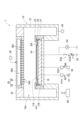
- チャンバと、
前記チャンバ内に設けられており、その上に載置される基板及びエッジリングを支持するように構成された基板支持部と、
前記チャンバ内でプラズマを生成するように構成されたプラズマ生成部と、
前記エッジリングに直流電圧を印加するように構成された直流電源と、
前記エッジリングの自己バイアス電位を測定するように構成されたセンサと、
前記プラズマ生成部及び前記直流電源を制御するように構成された制御部と、
を備え、
前記制御部は、
前記基板支持部上且つ前記エッジリングに囲まれた領域内に配置された基板を処理するために、前記チャンバ内でプラズマを生成するよう前記プラズマ生成部を制御し、
前記基板を処理するために前記チャンバ内で前記プラズマが生成されているときに、前記エッジリングに直流電圧を印加するよう前記直流電源を制御し、
前記基板を処理するために前記チャンバ内で前記プラズマが生成されているときに前記センサによって測定される前記エッジリングの自己バイアス電位に応じて、前記チャンバ内の表面のクリーニングを制御する、
よう構成されている、プラズマ処理装置。 - 前記制御部は、前記自己バイアス電位と閾値との比較により前記クリーニングが必要であると判定された場合に、前記クリーニングを行うための制御を実行するよう構成されている、請求項7に記載のプラズマ処理装置。
- 前記制御部は、前記チャンバ内で生成されたプラズマを用いて前記クリーニングが行われているときに測定される前記エッジリングの自己バイアス電位と閾値とを比較することにより前記クリーニングを終了すべきと判定された場合に、前記クリーニングを終了する制御を実行するよう構成されている、請求項7又は8に記載のプラズマ処理装置。
- 前記エッジリングの外周に沿って延在する導体部を更に備え、
前記直流電源は、前記導体部を介して前記エッジリングに前記直流電圧を印加するよう、前記導体部を介して前記エッジリングに電気的に接続されている、
請求項7~9の何れか一項に記載のプラズマ処理装置。 - 前記制御部は、前記基板を処理するために前記チャンバ内で前記プラズマが生成されているときに前記直流電圧の印加が停止されている状態で前記センサによって測定される前記自己バイアス電位を用いるよう構成されている、請求項7~10の何れか一項に記載のプラズマ処理装置。
- 前記クリーニングを、前記基板が前記チャンバから搬出された後の状態で又は前記基板と異なるダミー基板が前記基板支持部上に配置された状態で行うように構成された、請求項7~11の何れか一項に記載のプラズマ処理装置。
Priority Applications (5)
| Application Number | Priority Date | Filing Date | Title |
|---|---|---|---|
| JP2021089005A JP7579752B2 (ja) | 2021-05-27 | 2021-05-27 | クリーニングを制御する方法及びプラズマ処理装置 |
| CN202210534487.6A CN115410890A (zh) | 2021-05-27 | 2022-05-17 | 控制清洁的方法和等离子体处理装置 |
| KR1020220061289A KR20220160490A (ko) | 2021-05-27 | 2022-05-19 | 클리닝을 제어하는 방법 및 플라스마 처리 장치 |
| TW111118601A TW202312222A (zh) | 2021-05-27 | 2022-05-19 | 清洗控制方法及電漿處理裝置 |
| US17/748,446 US12009189B2 (en) | 2021-05-27 | 2022-05-19 | Method for controlling cleaning and plasma processing apparatus |
Applications Claiming Priority (1)
| Application Number | Priority Date | Filing Date | Title |
|---|---|---|---|
| JP2021089005A JP7579752B2 (ja) | 2021-05-27 | 2021-05-27 | クリーニングを制御する方法及びプラズマ処理装置 |
Publications (2)
| Publication Number | Publication Date |
|---|---|
| JP2022181831A JP2022181831A (ja) | 2022-12-08 |
| JP7579752B2 true JP7579752B2 (ja) | 2024-11-08 |
Family
ID=84157061
Family Applications (1)
| Application Number | Title | Priority Date | Filing Date |
|---|---|---|---|
| JP2021089005A Active JP7579752B2 (ja) | 2021-05-27 | 2021-05-27 | クリーニングを制御する方法及びプラズマ処理装置 |
Country Status (5)
| Country | Link |
|---|---|
| US (1) | US12009189B2 (ja) |
| JP (1) | JP7579752B2 (ja) |
| KR (1) | KR20220160490A (ja) |
| CN (1) | CN115410890A (ja) |
| TW (1) | TW202312222A (ja) |
Citations (4)
| Publication number | Priority date | Publication date | Assignee | Title |
|---|---|---|---|---|
| JP2004140096A (ja) | 2002-10-16 | 2004-05-13 | Seiko Epson Corp | プラズマ処理方法、プラズマ処理装置、プログラムおよび情報記憶媒体 |
| JP2017212445A (ja) | 2016-05-24 | 2017-11-30 | エスピーティーエス テクノロジーズ リミティド | プラズマ処理装置をクリーニングする方法 |
| JP2020113759A (ja) | 2019-01-11 | 2020-07-27 | 東京エレクトロン株式会社 | 処理方法及びプラズマ処理装置 |
| JP2021068880A (ja) | 2019-10-28 | 2021-04-30 | 東京エレクトロン株式会社 | 吸着方法、載置台及びプラズマ処理装置 |
Family Cites Families (8)
| Publication number | Priority date | Publication date | Assignee | Title |
|---|---|---|---|---|
| JP4554037B2 (ja) * | 2000-07-04 | 2010-09-29 | 東京エレクトロン株式会社 | 消耗品の消耗度予測方法及び堆積膜厚の予測方法 |
| US7578301B2 (en) * | 2005-03-28 | 2009-08-25 | Lam Research Corporation | Methods and apparatus for determining the endpoint of a cleaning or conditioning process in a plasma processing system |
| JP5281309B2 (ja) * | 2008-03-28 | 2013-09-04 | 東京エレクトロン株式会社 | プラズマエッチング装置及びプラズマエッチング方法及びコンピュータ読み取り可能な記憶媒体 |
| JP5227264B2 (ja) * | 2009-06-02 | 2013-07-03 | 東京エレクトロン株式会社 | プラズマ処理装置,プラズマ処理方法,プログラム |
| JP6826955B2 (ja) * | 2017-06-14 | 2021-02-10 | 東京エレクトロン株式会社 | プラズマ処理装置及びプラズマ処理方法 |
| JP2019169635A (ja) | 2018-03-23 | 2019-10-03 | 東京エレクトロン株式会社 | クリーニング方法及び処理装置 |
| JP7122864B2 (ja) | 2018-05-14 | 2022-08-22 | 東京エレクトロン株式会社 | クリーニング方法及び基板処理装置 |
| JP7145041B2 (ja) * | 2018-11-08 | 2022-09-30 | 東京エレクトロン株式会社 | 基板支持器、プラズマ処理装置、及びフォーカスリング |
-
2021
- 2021-05-27 JP JP2021089005A patent/JP7579752B2/ja active Active
-
2022
- 2022-05-17 CN CN202210534487.6A patent/CN115410890A/zh active Pending
- 2022-05-19 US US17/748,446 patent/US12009189B2/en active Active
- 2022-05-19 TW TW111118601A patent/TW202312222A/zh unknown
- 2022-05-19 KR KR1020220061289A patent/KR20220160490A/ko active Pending
Patent Citations (4)
| Publication number | Priority date | Publication date | Assignee | Title |
|---|---|---|---|---|
| JP2004140096A (ja) | 2002-10-16 | 2004-05-13 | Seiko Epson Corp | プラズマ処理方法、プラズマ処理装置、プログラムおよび情報記憶媒体 |
| JP2017212445A (ja) | 2016-05-24 | 2017-11-30 | エスピーティーエス テクノロジーズ リミティド | プラズマ処理装置をクリーニングする方法 |
| JP2020113759A (ja) | 2019-01-11 | 2020-07-27 | 東京エレクトロン株式会社 | 処理方法及びプラズマ処理装置 |
| JP2021068880A (ja) | 2019-10-28 | 2021-04-30 | 東京エレクトロン株式会社 | 吸着方法、載置台及びプラズマ処理装置 |
Also Published As
| Publication number | Publication date |
|---|---|
| US12009189B2 (en) | 2024-06-11 |
| KR20220160490A (ko) | 2022-12-06 |
| JP2022181831A (ja) | 2022-12-08 |
| US20220384162A1 (en) | 2022-12-01 |
| CN115410890A (zh) | 2022-11-29 |
| TW202312222A (zh) | 2023-03-16 |
Similar Documents
| Publication | Publication Date | Title |
|---|---|---|
| JP7519507B2 (ja) | プラズマ処理装置及びプラズマ処理方法 | |
| JP7519525B2 (ja) | 基板支持器及びプラズマ処理装置 | |
| US9966291B2 (en) | De-chuck control method and plasma processing apparatus | |
| TWI846014B (zh) | 電壓脈衝的時域多工 | |
| CN101990353B (zh) | 等离子处理装置和等离子处理方法 | |
| TWI764967B (zh) | 計測方法、除電方法及電漿處理裝置 | |
| CN113078040B (zh) | 等离子体处理装置及等离子体处理方法 | |
| JP2000012530A (ja) | エッチング方法、クリーニング方法、プラズマ処理装置及び整合回路 | |
| US20190066982A1 (en) | Measuring device, measurement method, and plasma processing device | |
| US9653317B2 (en) | Plasma processing method and plasma processing apparatus | |
| JP6339866B2 (ja) | プラズマ処理装置およびクリーニング方法 | |
| JP2020184551A (ja) | 除電方法及び基板処理装置 | |
| JP7325294B2 (ja) | プラズマ処理装置及びプラズマ処理方法 | |
| KR102751423B1 (ko) | 클리닝 처리 방법 및 플라즈마 처리 장치 | |
| JP7336395B2 (ja) | プラズマ処理装置及びプラズマ処理方法 | |
| JP7579752B2 (ja) | クリーニングを制御する方法及びプラズマ処理装置 | |
| JP7504686B2 (ja) | プラズマ処理装置及びプラズマ処理方法 | |
| US20240213002A1 (en) | Plasma processing method and plasma processing apparatus | |
| JP2023067369A (ja) | クリーニング方法、基板の処理方法及びプラズマ処理装置 |
Legal Events
| Date | Code | Title | Description |
|---|---|---|---|
| A621 | Written request for application examination |
Free format text: JAPANESE INTERMEDIATE CODE: A621 Effective date: 20231122 |
|
| A131 | Notification of reasons for refusal |
Free format text: JAPANESE INTERMEDIATE CODE: A131 Effective date: 20240716 |
|
| A977 | Report on retrieval |
Free format text: JAPANESE INTERMEDIATE CODE: A971007 Effective date: 20240717 |
|
| A521 | Request for written amendment filed |
Free format text: JAPANESE INTERMEDIATE CODE: A523 Effective date: 20240912 |
|
| TRDD | Decision of grant or rejection written | ||
| A01 | Written decision to grant a patent or to grant a registration (utility model) |
Free format text: JAPANESE INTERMEDIATE CODE: A01 Effective date: 20241001 |
|
| A61 | First payment of annual fees (during grant procedure) |
Free format text: JAPANESE INTERMEDIATE CODE: A61 Effective date: 20241028 |
|
| R150 | Certificate of patent or registration of utility model |
Ref document number: 7579752 Country of ref document: JP Free format text: JAPANESE INTERMEDIATE CODE: R150 |