JP7568826B2 - プローブカード - Google Patents
プローブカード Download PDFInfo
- Publication number
- JP7568826B2 JP7568826B2 JP2023506376A JP2023506376A JP7568826B2 JP 7568826 B2 JP7568826 B2 JP 7568826B2 JP 2023506376 A JP2023506376 A JP 2023506376A JP 2023506376 A JP2023506376 A JP 2023506376A JP 7568826 B2 JP7568826 B2 JP 7568826B2
- Authority
- JP
- Japan
- Prior art keywords
- coating
- probe card
- wiring board
- substrate
- heating
- Prior art date
- Legal status (The legal status is an assumption and is not a legal conclusion. Google has not performed a legal analysis and makes no representation as to the accuracy of the status listed.)
- Active
Links
Images


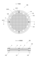


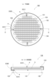


Classifications
-
- G—PHYSICS
- G01—MEASURING; TESTING
- G01R—MEASURING ELECTRIC VARIABLES; MEASURING MAGNETIC VARIABLES
- G01R1/00—Details of instruments or arrangements of the types included in groups G01R5/00 - G01R13/00 and G01R31/00
- G01R1/02—General constructional details
- G01R1/06—Measuring leads; Measuring probes
- G01R1/067—Measuring probes
- G01R1/073—Multiple probes
- G01R1/07307—Multiple probes with individual probe elements, e.g. needles, cantilever beams or bump contacts, fixed in relation to each other, e.g. bed of nails fixture or probe card
- G01R1/07314—Multiple probes with individual probe elements, e.g. needles, cantilever beams or bump contacts, fixed in relation to each other, e.g. bed of nails fixture or probe card the body of the probe being perpendicular to test object, e.g. bed of nails or probe with bump contacts on a rigid support
-
- G—PHYSICS
- G01—MEASURING; TESTING
- G01R—MEASURING ELECTRIC VARIABLES; MEASURING MAGNETIC VARIABLES
- G01R1/00—Details of instruments or arrangements of the types included in groups G01R5/00 - G01R13/00 and G01R31/00
- G01R1/02—General constructional details
- G01R1/06—Measuring leads; Measuring probes
- G01R1/067—Measuring probes
- G01R1/073—Multiple probes
- G01R1/07307—Multiple probes with individual probe elements, e.g. needles, cantilever beams or bump contacts, fixed in relation to each other, e.g. bed of nails fixture or probe card
- G01R1/07342—Multiple probes with individual probe elements, e.g. needles, cantilever beams or bump contacts, fixed in relation to each other, e.g. bed of nails fixture or probe card the body of the probe being at an angle other than perpendicular to test object, e.g. probe card
-
- G—PHYSICS
- G01—MEASURING; TESTING
- G01R—MEASURING ELECTRIC VARIABLES; MEASURING MAGNETIC VARIABLES
- G01R31/00—Arrangements for testing electric properties; Arrangements for locating electric faults; Arrangements for electrical testing characterised by what is being tested not provided for elsewhere
- G01R31/28—Testing of electronic circuits, e.g. by signal tracer
- G01R31/2851—Testing of integrated circuits [IC]
- G01R31/2855—Environmental, reliability or burn-in testing
- G01R31/2872—Environmental, reliability or burn-in testing related to electrical or environmental aspects, e.g. temperature, humidity, vibration, nuclear radiation
- G01R31/2874—Environmental, reliability or burn-in testing related to electrical or environmental aspects, e.g. temperature, humidity, vibration, nuclear radiation related to temperature
- G01R31/2875—Environmental, reliability or burn-in testing related to electrical or environmental aspects, e.g. temperature, humidity, vibration, nuclear radiation related to temperature related to heating
-
- H—ELECTRICITY
- H05—ELECTRIC TECHNIQUES NOT OTHERWISE PROVIDED FOR
- H05B—ELECTRIC HEATING; ELECTRIC LIGHT SOURCES NOT OTHERWISE PROVIDED FOR; CIRCUIT ARRANGEMENTS FOR ELECTRIC LIGHT SOURCES, IN GENERAL
- H05B3/00—Ohmic-resistance heating
- H05B3/02—Details
- H05B3/03—Electrodes
-
- H—ELECTRICITY
- H05—ELECTRIC TECHNIQUES NOT OTHERWISE PROVIDED FOR
- H05B—ELECTRIC HEATING; ELECTRIC LIGHT SOURCES NOT OTHERWISE PROVIDED FOR; CIRCUIT ARRANGEMENTS FOR ELECTRIC LIGHT SOURCES, IN GENERAL
- H05B3/00—Ohmic-resistance heating
- H05B3/20—Heating elements having extended surface area substantially in a two-dimensional [2D] plane, e.g. plate-heater
-
- H—ELECTRICITY
- H10—SEMICONDUCTOR DEVICES; ELECTRIC SOLID-STATE DEVICES NOT OTHERWISE PROVIDED FOR
- H10P—GENERIC PROCESSES OR APPARATUS FOR THE MANUFACTURE OR TREATMENT OF DEVICES COVERED BY CLASS H10
- H10P74/00—Testing or measuring during manufacture or treatment of wafers, substrates or devices
-
- G—PHYSICS
- G01—MEASURING; TESTING
- G01R—MEASURING ELECTRIC VARIABLES; MEASURING MAGNETIC VARIABLES
- G01R1/00—Details of instruments or arrangements of the types included in groups G01R5/00 - G01R13/00 and G01R31/00
- G01R1/02—General constructional details
- G01R1/06—Measuring leads; Measuring probes
- G01R1/067—Measuring probes
- G01R1/073—Multiple probes
- G01R1/07307—Multiple probes with individual probe elements, e.g. needles, cantilever beams or bump contacts, fixed in relation to each other, e.g. bed of nails fixture or probe card
- G01R1/07364—Multiple probes with individual probe elements, e.g. needles, cantilever beams or bump contacts, fixed in relation to each other, e.g. bed of nails fixture or probe card with provisions for altering position, number or connection of probe tips; Adapting to differences in pitch
- G01R1/07378—Multiple probes with individual probe elements, e.g. needles, cantilever beams or bump contacts, fixed in relation to each other, e.g. bed of nails fixture or probe card with provisions for altering position, number or connection of probe tips; Adapting to differences in pitch using an intermediate adapter, e.g. space transformers
-
- G—PHYSICS
- G01—MEASURING; TESTING
- G01R—MEASURING ELECTRIC VARIABLES; MEASURING MAGNETIC VARIABLES
- G01R31/00—Arrangements for testing electric properties; Arrangements for locating electric faults; Arrangements for electrical testing characterised by what is being tested not provided for elsewhere
- G01R31/28—Testing of electronic circuits, e.g. by signal tracer
- G01R31/2851—Testing of integrated circuits [IC]
- G01R31/2855—Environmental, reliability or burn-in testing
- G01R31/286—External aspects, e.g. related to chambers, contacting devices or handlers
- G01R31/2863—Contacting devices, e.g. sockets, burn-in boards or mounting fixtures
Landscapes
- Engineering & Computer Science (AREA)
- Physics & Mathematics (AREA)
- General Physics & Mathematics (AREA)
- Environmental & Geological Engineering (AREA)
- Health & Medical Sciences (AREA)
- Toxicology (AREA)
- Computer Hardware Design (AREA)
- Microelectronics & Electronic Packaging (AREA)
- General Engineering & Computer Science (AREA)
- Testing Or Measuring Of Semiconductors Or The Like (AREA)
- Measuring Leads Or Probes (AREA)
- Testing Of Individual Semiconductor Devices (AREA)
Applications Claiming Priority (1)
| Application Number | Priority Date | Filing Date | Title |
|---|---|---|---|
| PCT/JP2021/010294 WO2022195648A1 (ja) | 2021-03-15 | 2021-03-15 | プローブカード |
Publications (2)
| Publication Number | Publication Date |
|---|---|
| JPWO2022195648A1 JPWO2022195648A1 (https=) | 2022-09-22 |
| JP7568826B2 true JP7568826B2 (ja) | 2024-10-16 |
Family
ID=83320040
Family Applications (1)
| Application Number | Title | Priority Date | Filing Date |
|---|---|---|---|
| JP2023506376A Active JP7568826B2 (ja) | 2021-03-15 | 2021-03-15 | プローブカード |
Country Status (6)
| Country | Link |
|---|---|
| US (1) | US12467953B2 (https=) |
| JP (1) | JP7568826B2 (https=) |
| KR (1) | KR102825586B1 (https=) |
| CN (1) | CN116547543B (https=) |
| TW (1) | TWI795122B (https=) |
| WO (1) | WO2022195648A1 (https=) |
Families Citing this family (1)
| Publication number | Priority date | Publication date | Assignee | Title |
|---|---|---|---|---|
| JP7459368B2 (ja) * | 2021-02-19 | 2024-04-01 | 日本電子材料株式会社 | プローブカード用アライメントチップ、プローブカード及びプローブカード補修方法 |
Citations (2)
| Publication number | Priority date | Publication date | Assignee | Title |
|---|---|---|---|---|
| JP2000346875A (ja) | 1999-06-07 | 2000-12-15 | Advantest Corp | プローブカードおよびこれを用いたic試験装置 |
| JP2002532822A (ja) | 1998-12-04 | 2002-10-02 | ピージェイオー(インディサーム)リミテッド | 導電性材料 |
Family Cites Families (26)
| Publication number | Priority date | Publication date | Assignee | Title |
|---|---|---|---|---|
| US4567432A (en) * | 1983-06-09 | 1986-01-28 | Texas Instruments Incorporated | Apparatus for testing integrated circuits |
| JPH0196944A (ja) | 1987-10-08 | 1989-04-14 | Nec Corp | 高周波特性測定装置 |
| JPH05226430A (ja) * | 1992-02-10 | 1993-09-03 | Nitto Denko Corp | プローブカード構造体およびその製法 |
| JPH09321413A (ja) * | 1996-05-30 | 1997-12-12 | Hitachi Ltd | 電子回路基板の配線修正方法およびその装置 |
| JPH11154694A (ja) | 1997-11-21 | 1999-06-08 | Matsushita Electric Ind Co Ltd | ウェハ一括型測定検査用アライメント方法およびプローブカードの製造方法 |
| US6429671B1 (en) | 1998-11-25 | 2002-08-06 | Advanced Micro Devices, Inc. | Electrical test probe card having a removable probe head assembly with alignment features and a method for aligning the probe head assembly to the probe card |
| GB9826596D0 (en) | 1998-12-04 | 1999-01-27 | P J O Ind Limited | Conductive materials |
| JP2001330626A (ja) | 2000-05-22 | 2001-11-30 | Micronics Japan Co Ltd | プローブカード及びこれにアライメントマークを形成する方法 |
| JP2004233155A (ja) * | 2003-01-29 | 2004-08-19 | Fujitsu Ltd | プローブカードおよび半導体チップの検査方法 |
| KR200339049Y1 (ko) | 2003-10-13 | 2004-01-16 | 김영혜 | 이중 전압의 사용이 가능한 면상발열판을 구비한 히터 |
| JP4971636B2 (ja) | 2006-01-06 | 2012-07-11 | 川崎マイクロエレクトロニクス株式会社 | プローブカードの取り付け位置ずれの検出方法及びプローバ装置 |
| WO2008120575A1 (ja) | 2007-04-03 | 2008-10-09 | Advantest Corporation | コンタクタの実装方法 |
| KR100913916B1 (ko) * | 2008-04-17 | 2009-08-26 | (주)오리엔탈드림 | 발열체의 절연피막 형성방법 |
| JP5251395B2 (ja) * | 2008-09-24 | 2013-07-31 | 富士通株式会社 | 多層配線基板、プローブカード、及び、多層配線基板の製造方法 |
| JP5199859B2 (ja) | 2008-12-24 | 2013-05-15 | 株式会社日本マイクロニクス | プローブカード |
| JP2011117761A (ja) | 2009-12-01 | 2011-06-16 | Japan Electronic Materials Corp | プローブカードおよびプローブカードの製造方法 |
| JP6259590B2 (ja) * | 2013-06-12 | 2018-01-10 | 株式会社日本マイクロニクス | プローブカード及びその製造方法 |
| KR20160066678A (ko) * | 2014-12-02 | 2016-06-13 | 단국대학교 산학협력단 | 필름 히터 및 이를 구비한 프로브 스테이션 |
| JP6652443B2 (ja) * | 2016-05-06 | 2020-02-26 | 株式会社日本マイクロニクス | 多層配線基板及びこれを用いたプローブカード |
| JP6782103B2 (ja) * | 2016-06-21 | 2020-11-11 | 株式会社日本マイクロニクス | プローブカード、検査装置および検査方法 |
| JP6348626B2 (ja) | 2017-02-23 | 2018-06-27 | ルネサスエレクトロニクス株式会社 | 半導体装置の製造方法 |
| CN107132470A (zh) * | 2017-05-31 | 2017-09-05 | 格科微电子(上海)有限公司 | 适用于晶圆级测试的治具 |
| CN107523864B (zh) * | 2017-09-26 | 2024-12-17 | 深圳市石金科技股份有限公司 | 一种多晶硅铸锭炉的组合式加热器及多晶硅铸锭炉 |
| TWM587275U (zh) * | 2018-12-04 | 2019-12-01 | 蔚華科技股份有限公司 | 測試半導體設備之結構 |
| CN210657221U (zh) * | 2019-07-17 | 2020-06-02 | 浙江晶阳机电有限公司 | 一种硅芯铸锭炉用加热结构 |
| JP7459368B2 (ja) | 2021-02-19 | 2024-04-01 | 日本電子材料株式会社 | プローブカード用アライメントチップ、プローブカード及びプローブカード補修方法 |
-
2021
- 2021-03-15 CN CN202180077519.8A patent/CN116547543B/zh active Active
- 2021-03-15 WO PCT/JP2021/010294 patent/WO2022195648A1/ja not_active Ceased
- 2021-03-15 US US18/265,264 patent/US12467953B2/en active Active
- 2021-03-15 KR KR1020237015422A patent/KR102825586B1/ko active Active
- 2021-03-15 JP JP2023506376A patent/JP7568826B2/ja active Active
- 2021-12-13 TW TW110146541A patent/TWI795122B/zh active
Patent Citations (2)
| Publication number | Priority date | Publication date | Assignee | Title |
|---|---|---|---|---|
| JP2002532822A (ja) | 1998-12-04 | 2002-10-02 | ピージェイオー(インディサーム)リミテッド | 導電性材料 |
| JP2000346875A (ja) | 1999-06-07 | 2000-12-15 | Advantest Corp | プローブカードおよびこれを用いたic試験装置 |
Also Published As
| Publication number | Publication date |
|---|---|
| US12467953B2 (en) | 2025-11-11 |
| JPWO2022195648A1 (https=) | 2022-09-22 |
| KR102825586B1 (ko) | 2025-06-26 |
| TW202314258A (zh) | 2023-04-01 |
| CN116547543A (zh) | 2023-08-04 |
| WO2022195648A1 (ja) | 2022-09-22 |
| TW202238152A (zh) | 2022-10-01 |
| TWI795122B (zh) | 2023-03-01 |
| KR20230082670A (ko) | 2023-06-08 |
| US20240044942A1 (en) | 2024-02-08 |
| CN116547543B (zh) | 2026-01-27 |
Similar Documents
| Publication | Publication Date | Title |
|---|---|---|
| JP3685192B2 (ja) | 異方導電性コネクターおよび導電性ペースト組成物、プローブ部材並びにウエハ検査装置およびウエハ検査方法 | |
| JP5396112B2 (ja) | プローブカード | |
| TWI430525B (zh) | An aisotropic conductive connector, a probe member, and a wafer inspection device | |
| TWI758677B (zh) | 中介物、基座、基座組裝體及電路板組裝體 | |
| CN101930016A (zh) | 可替换式探针装置及其应用的探针卡 | |
| US9222961B1 (en) | Vertical probe card and method for manufacturing the same | |
| JP7568826B2 (ja) | プローブカード | |
| US20060091510A1 (en) | Probe card interposer | |
| JP3573120B2 (ja) | 異方導電性コネクターおよびその製造方法並びにその応用製品 | |
| JPH08306749A (ja) | プローブカードの製造方法 | |
| JPWO2009011201A1 (ja) | 検査用構造体 | |
| JP5104265B2 (ja) | プローブ部材およびその製造方法ならびにその応用 | |
| CN111751585A (zh) | 探针卡 | |
| TWI920406B (zh) | 探針卡 | |
| JP2007085833A (ja) | ウエハ検査用異方導電性コネクターおよびその製造方法、ウエハ検査用プローブカード並びにウエハ検査装置 | |
| JP2009098065A (ja) | プローブ部材およびその製造方法ならびにその応用 | |
| TW202542528A (zh) | 配線基板及電性連接裝置 | |
| KR100972995B1 (ko) | 프로브 본딩 방법 | |
| JP3781048B2 (ja) | シート状プローブおよびその応用 | |
| KR101068446B1 (ko) | 열 변형 보상 구조를 가진 프로브 카드 | |
| US20260002961A1 (en) | Metal Plated Conductive Elastomer Sort Probe | |
| KR101024098B1 (ko) | 프로브 본딩 방법 | |
| JP2001235492A (ja) | 回路基板の電気抵抗測定装置および測定方法 | |
| JP3596499B2 (ja) | 半導体検査装置の製造方法、半導体検査装置および半導体装置の検査方法 | |
| TW478085B (en) | Wafer level burn-in testing method |
Legal Events
| Date | Code | Title | Description |
|---|---|---|---|
| A621 | Written request for application examination |
Free format text: JAPANESE INTERMEDIATE CODE: A621 Effective date: 20230413 |
|
| RD01 | Notification of change of attorney |
Free format text: JAPANESE INTERMEDIATE CODE: A7421 Effective date: 20230823 |
|
| A521 | Request for written amendment filed |
Free format text: JAPANESE INTERMEDIATE CODE: A821 Effective date: 20230823 |
|
| A131 | Notification of reasons for refusal |
Free format text: JAPANESE INTERMEDIATE CODE: A131 Effective date: 20240626 |
|
| A521 | Request for written amendment filed |
Free format text: JAPANESE INTERMEDIATE CODE: A523 Effective date: 20240809 |
|
| TRDD | Decision of grant or rejection written | ||
| A01 | Written decision to grant a patent or to grant a registration (utility model) |
Free format text: JAPANESE INTERMEDIATE CODE: A01 Effective date: 20240920 |
|
| A61 | First payment of annual fees (during grant procedure) |
Free format text: JAPANESE INTERMEDIATE CODE: A61 Effective date: 20241003 |
|
| R150 | Certificate of patent or registration of utility model |
Ref document number: 7568826 Country of ref document: JP Free format text: JAPANESE INTERMEDIATE CODE: R150 |