JP7547536B2 - 深層学習人工ニューラルネットワークにおけるアナログニューラルメモリ用のデコーダ - Google Patents
深層学習人工ニューラルネットワークにおけるアナログニューラルメモリ用のデコーダ Download PDFInfo
- Publication number
- JP7547536B2 JP7547536B2 JP2023049721A JP2023049721A JP7547536B2 JP 7547536 B2 JP7547536 B2 JP 7547536B2 JP 2023049721 A JP2023049721 A JP 2023049721A JP 2023049721 A JP2023049721 A JP 2023049721A JP 7547536 B2 JP7547536 B2 JP 7547536B2
- Authority
- JP
- Japan
- Prior art keywords
- volatile memory
- word line
- array
- memory cells
- voltage
- Prior art date
- Legal status (The legal status is an assumption and is not a legal conclusion. Google has not performed a legal analysis and makes no representation as to the accuracy of the status listed.)
- Active
Links
Images


Classifications
-
- G—PHYSICS
- G06—COMPUTING OR CALCULATING; COUNTING
- G06N—COMPUTING ARRANGEMENTS BASED ON SPECIFIC COMPUTATIONAL MODELS
- G06N3/00—Computing arrangements based on biological models
- G06N3/02—Neural networks
- G06N3/06—Physical realisation, i.e. hardware implementation of neural networks, neurons or parts of neurons
- G06N3/063—Physical realisation, i.e. hardware implementation of neural networks, neurons or parts of neurons using electronic means
- G06N3/065—Analogue means
-
- G—PHYSICS
- G06—COMPUTING OR CALCULATING; COUNTING
- G06F—ELECTRIC DIGITAL DATA PROCESSING
- G06F17/00—Digital computing or data processing equipment or methods, specially adapted for specific functions
- G06F17/10—Complex mathematical operations
- G06F17/16—Matrix or vector computation, e.g. matrix-matrix or matrix-vector multiplication, matrix factorization
-
- G—PHYSICS
- G06—COMPUTING OR CALCULATING; COUNTING
- G06N—COMPUTING ARRANGEMENTS BASED ON SPECIFIC COMPUTATIONAL MODELS
- G06N3/00—Computing arrangements based on biological models
- G06N3/02—Neural networks
- G06N3/04—Architecture, e.g. interconnection topology
-
- G—PHYSICS
- G06—COMPUTING OR CALCULATING; COUNTING
- G06N—COMPUTING ARRANGEMENTS BASED ON SPECIFIC COMPUTATIONAL MODELS
- G06N3/00—Computing arrangements based on biological models
- G06N3/02—Neural networks
- G06N3/04—Architecture, e.g. interconnection topology
- G06N3/045—Combinations of networks
- G06N3/0455—Auto-encoder networks; Encoder-decoder networks
-
- G—PHYSICS
- G06—COMPUTING OR CALCULATING; COUNTING
- G06N—COMPUTING ARRANGEMENTS BASED ON SPECIFIC COMPUTATIONAL MODELS
- G06N3/00—Computing arrangements based on biological models
- G06N3/02—Neural networks
- G06N3/04—Architecture, e.g. interconnection topology
- G06N3/0464—Convolutional networks [CNN, ConvNet]
-
- G—PHYSICS
- G11—INFORMATION STORAGE
- G11C—STATIC STORES
- G11C11/00—Digital stores characterised by the use of particular electric or magnetic storage elements; Storage elements therefor
- G11C11/54—Digital stores characterised by the use of particular electric or magnetic storage elements; Storage elements therefor using elements simulating biological cells, e.g. neuron
-
- G—PHYSICS
- G11—INFORMATION STORAGE
- G11C—STATIC STORES
- G11C16/00—Erasable programmable read-only memories
- G11C16/02—Erasable programmable read-only memories electrically programmable
- G11C16/04—Erasable programmable read-only memories electrically programmable using variable threshold transistors, e.g. FAMOS
- G11C16/0408—Erasable programmable read-only memories electrically programmable using variable threshold transistors, e.g. FAMOS comprising cells containing floating gate transistors
- G11C16/0425—Erasable programmable read-only memories electrically programmable using variable threshold transistors, e.g. FAMOS comprising cells containing floating gate transistors comprising cells containing a merged floating gate and select transistor
-
- G—PHYSICS
- G11—INFORMATION STORAGE
- G11C—STATIC STORES
- G11C16/00—Erasable programmable read-only memories
- G11C16/02—Erasable programmable read-only memories electrically programmable
- G11C16/06—Auxiliary circuits, e.g. for writing into memory
- G11C16/08—Address circuits; Decoders; Word-line control circuits
-
- G—PHYSICS
- G11—INFORMATION STORAGE
- G11C—STATIC STORES
- G11C16/00—Erasable programmable read-only memories
- G11C16/02—Erasable programmable read-only memories electrically programmable
- G11C16/06—Auxiliary circuits, e.g. for writing into memory
- G11C16/24—Bit-line control circuits
-
- G—PHYSICS
- G11—INFORMATION STORAGE
- G11C—STATIC STORES
- G11C27/00—Electric analogue stores, e.g. for storing instantaneous values
- G11C27/02—Sample-and-hold arrangements
-
- G—PHYSICS
- G11—INFORMATION STORAGE
- G11C—STATIC STORES
- G11C2216/00—Indexing scheme relating to G11C16/00 and subgroups, for features not directly covered by these groups
- G11C2216/02—Structural aspects of erasable programmable read-only memories
- G11C2216/04—Nonvolatile memory cell provided with a separate control gate for erasing the cells, i.e. erase gate, independent of the normal read control gate
-
- G—PHYSICS
- G11—INFORMATION STORAGE
- G11C—STATIC STORES
- G11C2216/00—Indexing scheme relating to G11C16/00 and subgroups, for features not directly covered by these groups
- G11C2216/12—Reading and writing aspects of erasable programmable read-only memories
- G11C2216/14—Circuits or methods to write a page or sector of information simultaneously into a nonvolatile memory, typically a complete row or word line in flash memory
Landscapes
- Engineering & Computer Science (AREA)
- Physics & Mathematics (AREA)
- Theoretical Computer Science (AREA)
- General Physics & Mathematics (AREA)
- Mathematical Physics (AREA)
- Health & Medical Sciences (AREA)
- Life Sciences & Earth Sciences (AREA)
- Biomedical Technology (AREA)
- Data Mining & Analysis (AREA)
- Biophysics (AREA)
- Computing Systems (AREA)
- General Engineering & Computer Science (AREA)
- Software Systems (AREA)
- General Health & Medical Sciences (AREA)
- Molecular Biology (AREA)
- Computational Linguistics (AREA)
- Evolutionary Computation (AREA)
- Artificial Intelligence (AREA)
- Microelectronics & Electronic Packaging (AREA)
- Neurology (AREA)
- Mathematical Analysis (AREA)
- Computational Mathematics (AREA)
- Mathematical Optimization (AREA)
- Pure & Applied Mathematics (AREA)
- Algebra (AREA)
- Databases & Information Systems (AREA)
- Computer Hardware Design (AREA)
- Non-Volatile Memory (AREA)
- Read Only Memory (AREA)
Description
本出願は、2018年3月14日出願の「Decoders for Analog Neuromorphic Memory in Artificial Neural Network」と題された米国仮特許出願第62/642,884号、及び、2018年5月29日出願の「Decoders For Analog Neural Memory In Deep Learning Artificial Neural Network」と題された米国特許出願第15/991,890号に対する優先権を主張する。
人工ニューラルネットワークにおけるベクトルマトリクス乗算(VMM)アレイと共に使用するためのデコーダの多数の実施形態が開示される。
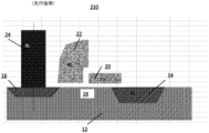
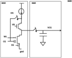
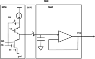
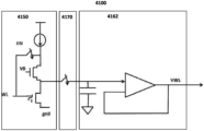
不揮発性メモリセル
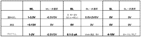
表1:図2のフラッシュメモリセル210の動作

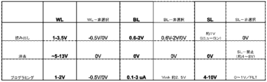
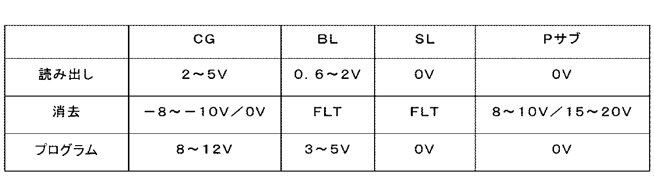
表2:図3のフラッシュメモリセル310の動作
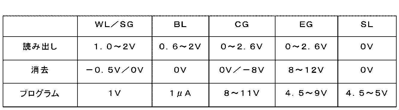
表3:図4のフラッシュメモリセル410の動作
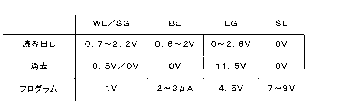
表4:図5のフラッシュメモリセル510の動作
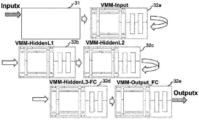
不揮発性メモリセルアレイを使用するニューラルネットワーク
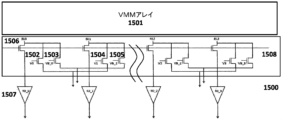
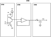
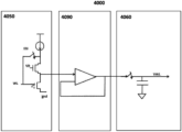
ベクトルマトリクス乗算(VMM)アレイ
Ids=Io*e(Vg-Vth)/kVt=w*Io*e(Vg)/kVt
w=e(-Vth)/kVt
Vg=k*Vt*log[Ids/wp*Io]
Iout=wa*Io*e(Vg)/kVt、すなわち
Iout=(wa/wp)*Iin=W*Iin
W=e(Vthp-Vtha)/kVt
Ids=β*(Vgs-Vth)*Vds;β=u*Cox*W/L
W α(Vgs-Vth)
Claims (2)
- アナログニューロモーフィックメモリシステムであって、
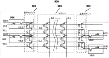
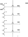
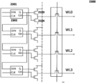
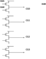
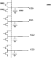
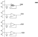
行及び列に編成された不揮発性メモリセルのアレイを備えるベクトルマトリクス乗算アレイであって、各不揮発性メモリセルは、ビット線端子、ワード線端子、及びソース線端子を含み、不揮発メモリセルの各行は、前記行内の前記不揮発メモリセルの前記ワード端子を介してワード線に接続され、かつ、前記行内の前記不揮発性メモリセルの前記ソース端子を線介してソース線に接続され、不揮発性メモリセルの各列は、前記列内の前記不揮発性メモリセルの前記ビット線端子を介してビット線に接続される、ベクトルマトリクス乗算アレイと、
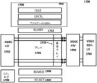
前記不揮発性メモリセルの前記ワード線端子に結合されたワード線デコーダ回路であって、低電圧又は高電圧を結合されたワード線端子に印加することができる、ワード線デコーダ回路と、
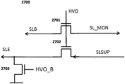
前記不揮発性メモリセルの前記ソース線端子に結合されたソース線デコーダ回路であって、前記ソース線デコーダ回路は、各行に対して、前記行の前記ソース線を低電圧に選択的に結合する第1のトランジスタ、及び、前記行の前記ソース線を高電圧に選択的に結合する第2のトランジスタを備える、ソース線デコーダ回路と、を備える、システム。 - 各不揮発性メモリセルは消去ゲート端子を更に備え、不揮発性メモリセルの各行は、前記行内の前記不揮発性メモリセルの前記消去ゲート端子を介して消去ゲート線に接続され、前記システムは、
前記不揮発性メモリセルの前記消去ゲート端子に結合された消去ゲートデコーダ回路であって、低電圧又は高電圧を結合された消去ゲート端子に印加することができる、消去ゲートデコーダ回路を更に備える、請求項1に記載のシステム。
Priority Applications (1)
| Application Number | Priority Date | Filing Date | Title |
|---|---|---|---|
| JP2024146132A JP7791950B2 (ja) | 2018-03-14 | 2024-08-28 | 深層学習人工ニューラルネットワークにおけるアナログニューラルメモリ用のデコーダ |
Applications Claiming Priority (5)
| Application Number | Priority Date | Filing Date | Title |
|---|---|---|---|
| US201862642884P | 2018-03-14 | 2018-03-14 | |
| US62/642,884 | 2018-03-14 | ||
| US15/991,890 US11087207B2 (en) | 2018-03-14 | 2018-05-29 | Decoders for analog neural memory in deep learning artificial neural network |
| US15/991,890 | 2018-05-29 | ||
| JP2020548740A JP7253563B2 (ja) | 2018-03-14 | 2019-01-24 | 深層学習人工ニューラルネットワークにおけるアナログニューラルメモリ用のデコーダ |
Related Parent Applications (1)
| Application Number | Title | Priority Date | Filing Date |
|---|---|---|---|
| JP2020548740A Division JP7253563B2 (ja) | 2018-03-14 | 2019-01-24 | 深層学習人工ニューラルネットワークにおけるアナログニューラルメモリ用のデコーダ |
Related Child Applications (1)
| Application Number | Title | Priority Date | Filing Date |
|---|---|---|---|
| JP2024146132A Division JP7791950B2 (ja) | 2018-03-14 | 2024-08-28 | 深層学習人工ニューラルネットワークにおけるアナログニューラルメモリ用のデコーダ |
Publications (2)
| Publication Number | Publication Date |
|---|---|
| JP2023093463A JP2023093463A (ja) | 2023-07-04 |
| JP7547536B2 true JP7547536B2 (ja) | 2024-09-09 |
Family
ID=67905831
Family Applications (3)
| Application Number | Title | Priority Date | Filing Date |
|---|---|---|---|
| JP2020548740A Active JP7253563B2 (ja) | 2018-03-14 | 2019-01-24 | 深層学習人工ニューラルネットワークにおけるアナログニューラルメモリ用のデコーダ |
| JP2023049721A Active JP7547536B2 (ja) | 2018-03-14 | 2023-03-27 | 深層学習人工ニューラルネットワークにおけるアナログニューラルメモリ用のデコーダ |
| JP2024146132A Active JP7791950B2 (ja) | 2018-03-14 | 2024-08-28 | 深層学習人工ニューラルネットワークにおけるアナログニューラルメモリ用のデコーダ |
Family Applications Before (1)
| Application Number | Title | Priority Date | Filing Date |
|---|---|---|---|
| JP2020548740A Active JP7253563B2 (ja) | 2018-03-14 | 2019-01-24 | 深層学習人工ニューラルネットワークにおけるアナログニューラルメモリ用のデコーダ |
Family Applications After (1)
| Application Number | Title | Priority Date | Filing Date |
|---|---|---|---|
| JP2024146132A Active JP7791950B2 (ja) | 2018-03-14 | 2024-08-28 | 深層学習人工ニューラルネットワークにおけるアナログニューラルメモリ用のデコーダ |
Country Status (7)
| Country | Link |
|---|---|
| US (4) | US11087207B2 (ja) |
| EP (4) | EP4650990A2 (ja) |
| JP (3) | JP7253563B2 (ja) |
| KR (4) | KR20250035044A (ja) |
| CN (2) | CN119599075A (ja) |
| TW (2) | TWI764503B (ja) |
| WO (1) | WO2019177698A1 (ja) |
Families Citing this family (28)
| Publication number | Priority date | Publication date | Assignee | Title |
|---|---|---|---|---|
| US10891080B1 (en) * | 2018-06-04 | 2021-01-12 | Mentium Technologies Inc. | Management of non-volatile memory arrays |
| US11500442B2 (en) * | 2019-01-18 | 2022-11-15 | Silicon Storage Technology, Inc. | System for converting neuron current into neuron current-based time pulses in an analog neural memory in a deep learning artificial neural network |
| US11893478B2 (en) | 2019-01-18 | 2024-02-06 | Silicon Storage Technology, Inc. | Programmable output blocks for analog neural memory in a deep learning artificial neural network |
| US11270763B2 (en) | 2019-01-18 | 2022-03-08 | Silicon Storage Technology, Inc. | Neural network classifier using array of three-gate non-volatile memory cells |
| US11023559B2 (en) | 2019-01-25 | 2021-06-01 | Microsemi Soc Corp. | Apparatus and method for combining analog neural net with FPGA routing in a monolithic integrated circuit |
| US11423979B2 (en) | 2019-04-29 | 2022-08-23 | Silicon Storage Technology, Inc. | Decoding system and physical layout for analog neural memory in deep learning artificial neural network |
| CN111313914B (zh) * | 2019-11-05 | 2021-09-28 | 北京航空航天大学 | 一种基于神经网络分类器的scl简化译码方法 |
| US12124942B2 (en) * | 2019-12-03 | 2024-10-22 | Anaflash Inc. | Serialized neural network computing unit |
| TWI789589B (zh) * | 2020-02-04 | 2023-01-11 | 旺宏電子股份有限公司 | 脈衝神經網路電路及其運作方法 |
| US11600321B2 (en) * | 2020-03-05 | 2023-03-07 | Silicon Storage Technology, Inc. | Analog neural memory array storing synapsis weights in differential cell pairs in artificial neural network |
| KR102899213B1 (ko) | 2020-03-25 | 2025-12-10 | 삼성전자주식회사 | 뉴로모픽 장치 및 그 구동 방법 |
| US11289164B2 (en) * | 2020-06-03 | 2022-03-29 | Silicon Storage Technology, Inc. | Word line and control gate line tandem decoder for analog neural memory in deep learning artificial neural network |
| US11875852B2 (en) * | 2020-07-06 | 2024-01-16 | Silicon Storage Technology, Inc. | Adaptive bias decoder to provide a voltage to a control gate line in an analog neural memory array in artificial neural network |
| CN113946278B (zh) * | 2020-07-16 | 2025-01-21 | 慧荣科技股份有限公司 | 主机效能加速模式的数据读取方法及装置 |
| FR3113326B1 (fr) * | 2020-08-06 | 2023-01-06 | St Microelectronics Rousset | Procédé de calcul convolutif intra-mémoire et circuit intégré correspondant |
| CN112633487B (zh) * | 2020-12-25 | 2022-05-20 | 北京大学 | 一种卷积神经网络最大池化层电路 |
| CN112784971A (zh) * | 2021-01-13 | 2021-05-11 | 天津智模科技有限公司 | 基于数模混合神经元的神经网络运算电路 |
| US12033699B2 (en) * | 2021-02-02 | 2024-07-09 | Macronix International Co., Ltd. | Memory device and operation method thereof for performing multiply accumulate operation |
| TWI821746B (zh) * | 2021-02-02 | 2023-11-11 | 旺宏電子股份有限公司 | 記憶體裝置及其操作方法 |
| EP4668165A2 (en) * | 2021-05-18 | 2025-12-24 | Silicon Storage Technology, Inc. | Split array architecture for analog neural memory in a deep learning artificial neural network |
| US11996137B2 (en) * | 2021-05-21 | 2024-05-28 | Taiwan Semiconductor Manufacturing Company, Ltd. | Compute in memory (CIM) memory array |
| US20230048411A1 (en) * | 2021-08-02 | 2023-02-16 | Silicon Storage Technology, Inc. | Input circuitry for analog neural memory in a deep learning artificial neural network |
| US11935603B2 (en) * | 2021-11-04 | 2024-03-19 | Infineon Technologies LLC | Erase power loss indicator (EPLI) implementation in flash memory device |
| US12499943B2 (en) | 2022-01-06 | 2025-12-16 | Samsung Electronics Co., Ltd. | Spiking neural network device, nonvolatile memory device, and operation method thereof |
| KR20230166777A (ko) | 2022-05-31 | 2023-12-07 | 삼성전자주식회사 | 뉴로모픽 장치 |
| CN115688897B (zh) * | 2023-01-03 | 2023-03-31 | 浙江大学杭州国际科创中心 | 低功耗紧凑型Relu激活函数神经元电路 |
| KR102885729B1 (ko) * | 2023-03-31 | 2025-11-13 | 서울대학교산학협력단 | 업데이트 셀과 이를 포함하는 뉴로모픽 회로 및 뉴로모픽 회로의 동작 방법 |
| CN120981817A (zh) * | 2023-03-31 | 2025-11-18 | 首尔大学校产学协力团 | 更新单元、包括其的神经形态电路以及神经形态电路的操作方法 |
Citations (2)
| Publication number | Priority date | Publication date | Assignee | Title |
|---|---|---|---|---|
| WO2017200883A1 (en) | 2016-05-17 | 2017-11-23 | Silicon Storage Technology, Inc. | Deep learning neural network classifier using non-volatile memory array |
| WO2017200888A1 (en) | 2016-05-18 | 2017-11-23 | Silicon Storage Technology, Inc. | Improved flash memory cell associated decoders |
Family Cites Families (85)
| Publication number | Priority date | Publication date | Assignee | Title |
|---|---|---|---|---|
| FR2603414B1 (fr) | 1986-08-29 | 1988-10-28 | Bull Sa | Amplificateur de lecture |
| JP3122756B2 (ja) | 1991-01-12 | 2001-01-09 | 直 柴田 | 半導体装置 |
| US5621336A (en) | 1989-06-02 | 1997-04-15 | Shibata; Tadashi | Neuron circuit |
| JPH0318985A (ja) | 1989-06-16 | 1991-01-28 | Hitachi Ltd | 情報処理装置 |
| US4961002A (en) | 1989-07-13 | 1990-10-02 | Intel Corporation | Synapse cell employing dual gate transistor structure |
| GB2236881B (en) * | 1989-10-11 | 1994-01-12 | Intel Corp | Improved synapse cell employing dual gate transistor structure |
| KR920010344B1 (ko) | 1989-12-29 | 1992-11-27 | 삼성전자주식회사 | 반도체 메모리 어레이의 구성방법 |
| US5029130A (en) | 1990-01-22 | 1991-07-02 | Silicon Storage Technology, Inc. | Single transistor non-valatile electrically alterable semiconductor memory device |
| US5146602A (en) | 1990-12-26 | 1992-09-08 | Intel Corporation | Method of increasing the accuracy of an analog neural network and the like |
| US5138576A (en) | 1991-11-06 | 1992-08-11 | Altera Corporation | Method and apparatus for erasing an array of electrically erasable EPROM cells |
| DE69319162T2 (de) | 1992-03-26 | 1999-03-25 | Hitachi Vlsi Engineering Corp., Kodaira, Tokio/Tokyo | Flash-Speicher |
| US5336936A (en) | 1992-05-06 | 1994-08-09 | Synaptics, Incorporated | One-transistor adaptable analog storage element and array |
| US5264734A (en) | 1992-05-19 | 1993-11-23 | Intel Corporation | Difference calculating neural network utilizing switched capacitors |
| US5256911A (en) | 1992-06-10 | 1993-10-26 | Intel Corporation | Neural network with multiplexed snyaptic processing |
| JPH0628875A (ja) * | 1992-07-10 | 1994-02-04 | Sony Corp | フラッシュ型e2 promの消去方法 |
| US5386132A (en) | 1992-11-02 | 1995-01-31 | Wong; Chun C. D. | Multimedia storage system with highly compact memory device |
| JP2835272B2 (ja) | 1993-12-21 | 1998-12-14 | 株式会社東芝 | 半導体記憶装置 |
| KR0151623B1 (ko) | 1994-12-07 | 1998-10-01 | 문정환 | 이이피롬 셀 및 그 제조방법 |
| US5825063A (en) | 1995-03-07 | 1998-10-20 | California Institute Of Technology | Three-terminal silicon synaptic device |
| US5554874A (en) | 1995-06-05 | 1996-09-10 | Quantum Effect Design, Inc. | Six-transistor cell with wide bit-line pitch, double words lines, and bit-line contact shared among four cells |
| US5721702A (en) | 1995-08-01 | 1998-02-24 | Micron Quantum Devices, Inc. | Reference voltage generator using flash memory cells |
| US6683645B1 (en) | 1995-12-01 | 2004-01-27 | Qinetiq Limited | Imaging system with low sensitivity to variation in scene illumination |
| JPH10320989A (ja) * | 1997-05-16 | 1998-12-04 | Toshiba Microelectron Corp | 不揮発性半導体メモリ |
| TW332954B (en) * | 1997-05-16 | 1998-06-01 | Ind Tech Res Inst | Data processing method and apparatus in neural network system |
| US6222777B1 (en) | 1999-04-09 | 2001-04-24 | Sun Microsystems, Inc. | Output circuit for alternating multiple bit line per column memory architecture |
| KR100338772B1 (ko) | 2000-03-10 | 2002-05-31 | 윤종용 | 바이어스 라인이 분리된 비휘발성 메모리 장치의 워드라인 드라이버 및 워드 라인 드라이빙 방법 |
| US6829598B2 (en) | 2000-10-02 | 2004-12-07 | Texas Instruments Incorporated | Method and apparatus for modeling a neural synapse function by utilizing a single conventional MOSFET |
| US6563167B2 (en) | 2001-01-05 | 2003-05-13 | Silicon Storage Technology, Inc. | Semiconductor memory array of floating gate memory cells with floating gates having multiple sharp edges |
| US6563733B2 (en) | 2001-05-24 | 2003-05-13 | Winbond Electronics Corporation | Memory array architectures based on a triple-polysilicon source-side injection non-volatile memory cell |
| US6912152B2 (en) * | 2002-02-22 | 2005-06-28 | Kabushiki Kaisha Toshiba | Magnetic random access memory |
| JP2005522071A (ja) | 2002-03-22 | 2005-07-21 | ジョージア テック リサーチ コーポレイション | 浮遊ゲートアナログ回路 |
| JP4273718B2 (ja) | 2002-08-16 | 2009-06-03 | ソニー株式会社 | 電流サンプリング回路及びそれを用いた電流出力型駆動回路 |
| US6747310B2 (en) | 2002-10-07 | 2004-06-08 | Actrans System Inc. | Flash memory cells with separated self-aligned select and erase gates, and process of fabrication |
| ITMI20022240A1 (it) * | 2002-10-22 | 2004-04-23 | Atmel Corp | Architettura di memoria flash con cancellazione di modo |
| JP2004171686A (ja) | 2002-11-20 | 2004-06-17 | Renesas Technology Corp | 不揮発性半導体記憶装置およびそのデータ消去方法 |
| US6822910B2 (en) | 2002-12-29 | 2004-11-23 | Macronix International Co., Ltd. | Non-volatile memory and operating method thereof |
| US6856551B2 (en) | 2003-02-06 | 2005-02-15 | Sandisk Corporation | System and method for programming cells in non-volatile integrated memory devices |
| TWI220560B (en) | 2003-10-27 | 2004-08-21 | Powerchip Semiconductor Corp | NAND flash memory cell architecture, NAND flash memory cell array, manufacturing method and operating method of the same |
| JP4585213B2 (ja) * | 2004-03-24 | 2010-11-24 | 株式会社日立製作所 | データ保護方法及び認証方法並びにプログラム |
| JP4157065B2 (ja) * | 2004-03-29 | 2008-09-24 | 株式会社東芝 | 半導体記憶装置 |
| US7315056B2 (en) | 2004-06-07 | 2008-01-01 | Silicon Storage Technology, Inc. | Semiconductor memory array of floating gate memory cells with program/erase and select gates |
| KR100632946B1 (ko) | 2004-07-13 | 2006-10-12 | 삼성전자주식회사 | 불 휘발성 메모리 장치 및 그것의 프로그램 방법 |
| US7092290B2 (en) | 2004-11-16 | 2006-08-15 | Sandisk Corporation | High speed programming system with reduced over programming |
| TWI270199B (en) | 2005-01-31 | 2007-01-01 | Powerchip Semiconductor Corp | Non-volatile memory and manufacturing method and operating method thereof |
| US7304890B2 (en) | 2005-12-13 | 2007-12-04 | Atmel Corporation | Double byte select high voltage line for EEPROM memory block |
| US7626868B1 (en) | 2007-05-04 | 2009-12-01 | Flashsilicon, Incorporation | Level verification and adjustment for multi-level cell (MLC) non-volatile memory (NVM) |
| US7630246B2 (en) | 2007-06-18 | 2009-12-08 | Micron Technology, Inc. | Programming rate identification and control in a solid state memory |
| JP5045294B2 (ja) | 2007-07-30 | 2012-10-10 | 富士通セミコンダクター株式会社 | カスコードカレントミラー回路を有する内部電源回路 |
| US20090039410A1 (en) | 2007-08-06 | 2009-02-12 | Xian Liu | Split Gate Non-Volatile Flash Memory Cell Having A Floating Gate, Control Gate, Select Gate And An Erase Gate With An Overhang Over The Floating Gate, Array And Method Of Manufacturing |
| US7800159B2 (en) * | 2007-10-24 | 2010-09-21 | Silicon Storage Technology, Inc. | Array of contactless non-volatile memory cells |
| US7894267B2 (en) | 2007-10-30 | 2011-02-22 | Spansion Llc | Deterministic programming algorithm that provides tighter cell distributions with a reduced number of programming pulses |
| US8464123B2 (en) * | 2009-05-07 | 2013-06-11 | Ramot At Tel Aviv University Ltd. | Matrix structure for block encoding |
| JP2010267341A (ja) | 2009-05-15 | 2010-11-25 | Renesas Electronics Corp | 半導体装置 |
| US8553466B2 (en) * | 2010-03-04 | 2013-10-08 | Samsung Electronics Co., Ltd. | Non-volatile memory device, erasing method thereof, and memory system including the same |
| US8325521B2 (en) | 2010-10-08 | 2012-12-04 | Taiwan Semiconductor Manufacturing Company, Ltd. | Structure and inhibited operation of flash memory with split gate |
| US8892487B2 (en) | 2010-12-30 | 2014-11-18 | International Business Machines Corporation | Electronic synapses for reinforcement learning |
| JP2013041654A (ja) | 2011-08-19 | 2013-02-28 | Toshiba Corp | 不揮発性記憶装置 |
| US8909576B2 (en) | 2011-09-16 | 2014-12-09 | International Business Machines Corporation | Neuromorphic event-driven neural computing architecture in a scalable neural network |
| US8760955B2 (en) | 2011-10-21 | 2014-06-24 | Taiwan Semiconductor Manufacturing Company, Ltd. | Electrical fuse memory arrays |
| JP3174679U (ja) | 2012-01-20 | 2012-03-29 | 株式会社エラン | 撃針部およびブローバックモデルガン |
| US9466732B2 (en) | 2012-08-23 | 2016-10-11 | Silicon Storage Technology, Inc. | Split-gate memory cell with depletion-mode floating gate channel, and method of making same |
| US9275748B2 (en) | 2013-03-14 | 2016-03-01 | Silicon Storage Technology, Inc. | Low leakage, low threshold voltage, split-gate flash cell operation |
| US10095718B2 (en) | 2013-10-16 | 2018-10-09 | University Of Tennessee Research Foundation | Method and apparatus for constructing a dynamic adaptive neural network array (DANNA) |
| US20150213898A1 (en) | 2014-01-27 | 2015-07-30 | Silicon Storage Technololgy, Inc. | Byte Erasable Non-volatile Memory Architecture And Method Of Erasing Same |
| US9431111B2 (en) * | 2014-07-08 | 2016-08-30 | Ememory Technology Inc. | One time programming memory cell, array structure and operating method thereof |
| US9286982B2 (en) | 2014-08-08 | 2016-03-15 | Silicon Storage Technology, Inc. | Flash memory system with EEPROM functionality |
| US9984754B2 (en) | 2014-09-29 | 2018-05-29 | Toshiba Memory Corporation | Memory device and method for operating the same |
| US10312248B2 (en) | 2014-11-12 | 2019-06-04 | Silicon Storage Technology, Inc. | Virtual ground non-volatile memory array |
| US9361991B1 (en) | 2014-12-23 | 2016-06-07 | Sandisk Technologies Inc. | Efficient scanning of nonvolatile memory blocks |
| CN105990367B (zh) | 2015-02-27 | 2019-03-12 | 硅存储技术公司 | 具有rom单元的非易失性存储器单元阵列 |
| US9595332B2 (en) * | 2015-06-15 | 2017-03-14 | Cypress Semiconductor Corporation | High speed, high voltage tolerant circuits in flash path |
| KR102473665B1 (ko) * | 2015-07-28 | 2022-12-02 | 삼성전자주식회사 | 스토리지 디바이스 및 스토리지 가상화 시스템 |
| US10014318B2 (en) * | 2015-10-24 | 2018-07-03 | Monocithic 3D Inc | Semiconductor memory device, structure and methods |
| US10418369B2 (en) * | 2015-10-24 | 2019-09-17 | Monolithic 3D Inc. | Multi-level semiconductor memory device and structure |
| US10269440B2 (en) | 2016-05-17 | 2019-04-23 | Silicon Storage Technology, Inc. | Flash memory array with individual memory cell read, program and erase |
| KR102384654B1 (ko) | 2016-05-17 | 2022-04-11 | 실리콘 스토리지 테크놀로지 인크 | 개별 메모리 셀 판독, 프로그래밍, 및 소거를 갖는 3-게이트 플래시 메모리 셀들의 어레이 |
| US9910827B2 (en) | 2016-07-01 | 2018-03-06 | Hewlett Packard Enterprise Development Lp | Vector-matrix multiplications involving negative values |
| US10748059B2 (en) | 2017-04-05 | 2020-08-18 | International Business Machines Corporation | Architecture for an electrochemical artificial neural network |
| US10134472B1 (en) * | 2017-06-30 | 2018-11-20 | International Business Machines Corporation | Floating gate architecture for deep neural network application |
| US10460817B2 (en) * | 2017-07-13 | 2019-10-29 | Qualcomm Incorporated | Multiple (multi-) level cell (MLC) non-volatile (NV) memory (NVM) matrix circuits for performing matrix computations with multi-bit input vectors |
| CN109522753B (zh) | 2017-09-18 | 2020-11-06 | 清华大学 | 电路结构及其驱动方法、芯片及其认证方法、电子设备 |
| US10803943B2 (en) | 2017-11-29 | 2020-10-13 | Silicon Storage Technology, Inc. | Neural network classifier using array of four-gate non-volatile memory cells |
| US11354562B2 (en) * | 2018-01-03 | 2022-06-07 | Silicon Storage Technology, Inc. | Programmable neuron for analog non-volatile memory in deep learning artificial neural network |
| US10970441B1 (en) * | 2018-02-26 | 2021-04-06 | Washington University | System and method using neural networks for analog-to-information processors |
| US11270763B2 (en) | 2019-01-18 | 2022-03-08 | Silicon Storage Technology, Inc. | Neural network classifier using array of three-gate non-volatile memory cells |
-
2018
- 2018-05-29 US US15/991,890 patent/US11087207B2/en active Active
-
2019
- 2019-01-24 KR KR1020257007057A patent/KR20250035044A/ko active Pending
- 2019-01-24 KR KR1020207022363A patent/KR102516399B1/ko active Active
- 2019-01-24 KR KR1020237010513A patent/KR102604405B1/ko active Active
- 2019-01-24 EP EP25206286.4A patent/EP4650990A2/en active Pending
- 2019-01-24 CN CN202411640536.XA patent/CN119599075A/zh active Pending
- 2019-01-24 EP EP23212305.9A patent/EP4303772B1/en active Active
- 2019-01-24 EP EP19766740.5A patent/EP3766178B1/en active Active
- 2019-01-24 KR KR1020237039451A patent/KR102778708B1/ko active Active
- 2019-01-24 JP JP2020548740A patent/JP7253563B2/ja active Active
- 2019-01-24 WO PCT/US2019/015022 patent/WO2019177698A1/en not_active Ceased
- 2019-01-24 CN CN201980018434.5A patent/CN111886804B/zh active Active
- 2019-01-24 EP EP25206284.9A patent/EP4650989A2/en active Pending
- 2019-03-11 TW TW110100981A patent/TWI764503B/zh active
- 2019-03-11 TW TW108108059A patent/TWI717703B/zh active
-
2021
- 2021-07-06 US US17/367,633 patent/US12099921B2/en active Active
-
2023
- 2023-03-27 JP JP2023049721A patent/JP7547536B2/ja active Active
- 2023-11-27 US US18/520,277 patent/US20240095508A1/en active Pending
- 2023-11-27 US US18/520,500 patent/US12248870B2/en active Active
-
2024
- 2024-08-28 JP JP2024146132A patent/JP7791950B2/ja active Active
Patent Citations (4)
| Publication number | Priority date | Publication date | Assignee | Title |
|---|---|---|---|---|
| WO2017200883A1 (en) | 2016-05-17 | 2017-11-23 | Silicon Storage Technology, Inc. | Deep learning neural network classifier using non-volatile memory array |
| JP2019517138A (ja) | 2016-05-17 | 2019-06-20 | シリコン ストーリッジ テクノロージー インコーポレイテッドSilicon Storage Technology, Inc. | 不揮発性メモリアレイを使用したディープラーニングニューラルネットワーク分類器 |
| WO2017200888A1 (en) | 2016-05-18 | 2017-11-23 | Silicon Storage Technology, Inc. | Improved flash memory cell associated decoders |
| JP2019519059A (ja) | 2016-05-18 | 2019-07-04 | シリコン ストーリッジ テクノロージー インコーポレイテッドSilicon Storage Technology, Inc. | 改善されたフラッシュメモリセル及び関連するデコーダ |
Also Published As
Similar Documents
| Publication | Publication Date | Title |
|---|---|---|
| JP7547536B2 (ja) | 深層学習人工ニューラルネットワークにおけるアナログニューラルメモリ用のデコーダ | |
| JP7668307B2 (ja) | 深層学習人工ニューラルネットワークにおけるアナログニューラルメモリ用のデコードシステム及び物理レイアウト | |
| JP7209811B2 (ja) | 深層学習ニューラルネットワーク用の構成可能なアナログニューラルメモリシステム | |
| JP7620059B2 (ja) | 深層学習人工ニューラルネットワークにおけるアナログニューラルメモリのためのワード線及び制御ゲート線タンデムデコーダ | |
| KR102912832B1 (ko) | 딥 러닝 인공 신경 네트워크 내의 아날로그 신경 메모리를 위한 디코딩 시스템 및 물리적 레이아웃 | |
| KR20260017002A (ko) | 딥 러닝 인공 신경 네트워크 내의 아날로그 신경 메모리를 위한 디코딩 시스템 및 물리적 레이아웃 |
Legal Events
| Date | Code | Title | Description |
|---|---|---|---|
| A521 | Request for written amendment filed |
Free format text: JAPANESE INTERMEDIATE CODE: A523 Effective date: 20230424 |
|
| A621 | Written request for application examination |
Free format text: JAPANESE INTERMEDIATE CODE: A621 Effective date: 20230424 |
|
| A131 | Notification of reasons for refusal |
Free format text: JAPANESE INTERMEDIATE CODE: A131 Effective date: 20240416 |
|
| A521 | Request for written amendment filed |
Free format text: JAPANESE INTERMEDIATE CODE: A523 Effective date: 20240716 |
|
| TRDD | Decision of grant or rejection written | ||
| A01 | Written decision to grant a patent or to grant a registration (utility model) |
Free format text: JAPANESE INTERMEDIATE CODE: A01 Effective date: 20240730 |
|
| A61 | First payment of annual fees (during grant procedure) |
Free format text: JAPANESE INTERMEDIATE CODE: A61 Effective date: 20240828 |
|
| R150 | Certificate of patent or registration of utility model |
Ref document number: 7547536 Country of ref document: JP Free format text: JAPANESE INTERMEDIATE CODE: R150 |