JP7547536B2 - Decoders for Analog Neural Memories in Deep Learning Artificial Neural Networks - Google Patents
Decoders for Analog Neural Memories in Deep Learning Artificial Neural Networks Download PDFInfo
- Publication number
- JP7547536B2 JP7547536B2 JP2023049721A JP2023049721A JP7547536B2 JP 7547536 B2 JP7547536 B2 JP 7547536B2 JP 2023049721 A JP2023049721 A JP 2023049721A JP 2023049721 A JP2023049721 A JP 2023049721A JP 7547536 B2 JP7547536 B2 JP 7547536B2
- Authority
- JP
- Japan
- Prior art keywords
- volatile memory
- word line
- array
- memory cells
- voltage
- Prior art date
- Legal status (The legal status is an assumption and is not a legal conclusion. Google has not performed a legal analysis and makes no representation as to the accuracy of the status listed.)
- Active
Links
Images


Classifications
-
- G—PHYSICS
- G06—COMPUTING OR CALCULATING; COUNTING
- G06N—COMPUTING ARRANGEMENTS BASED ON SPECIFIC COMPUTATIONAL MODELS
- G06N3/00—Computing arrangements based on biological models
- G06N3/02—Neural networks
- G06N3/06—Physical realisation, i.e. hardware implementation of neural networks, neurons or parts of neurons
- G06N3/063—Physical realisation, i.e. hardware implementation of neural networks, neurons or parts of neurons using electronic means
- G06N3/065—Analogue means
-
- G—PHYSICS
- G06—COMPUTING OR CALCULATING; COUNTING
- G06F—ELECTRIC DIGITAL DATA PROCESSING
- G06F17/00—Digital computing or data processing equipment or methods, specially adapted for specific functions
- G06F17/10—Complex mathematical operations
- G06F17/16—Matrix or vector computation, e.g. matrix-matrix or matrix-vector multiplication, matrix factorization
-
- G—PHYSICS
- G06—COMPUTING OR CALCULATING; COUNTING
- G06N—COMPUTING ARRANGEMENTS BASED ON SPECIFIC COMPUTATIONAL MODELS
- G06N3/00—Computing arrangements based on biological models
- G06N3/02—Neural networks
- G06N3/04—Architecture, e.g. interconnection topology
-
- G—PHYSICS
- G06—COMPUTING OR CALCULATING; COUNTING
- G06N—COMPUTING ARRANGEMENTS BASED ON SPECIFIC COMPUTATIONAL MODELS
- G06N3/00—Computing arrangements based on biological models
- G06N3/02—Neural networks
- G06N3/04—Architecture, e.g. interconnection topology
- G06N3/045—Combinations of networks
- G06N3/0455—Auto-encoder networks; Encoder-decoder networks
-
- G—PHYSICS
- G06—COMPUTING OR CALCULATING; COUNTING
- G06N—COMPUTING ARRANGEMENTS BASED ON SPECIFIC COMPUTATIONAL MODELS
- G06N3/00—Computing arrangements based on biological models
- G06N3/02—Neural networks
- G06N3/04—Architecture, e.g. interconnection topology
- G06N3/0464—Convolutional networks [CNN, ConvNet]
-
- G—PHYSICS
- G11—INFORMATION STORAGE
- G11C—STATIC STORES
- G11C11/00—Digital stores characterised by the use of particular electric or magnetic storage elements; Storage elements therefor
- G11C11/54—Digital stores characterised by the use of particular electric or magnetic storage elements; Storage elements therefor using elements simulating biological cells, e.g. neuron
-
- G—PHYSICS
- G11—INFORMATION STORAGE
- G11C—STATIC STORES
- G11C16/00—Erasable programmable read-only memories
- G11C16/02—Erasable programmable read-only memories electrically programmable
- G11C16/04—Erasable programmable read-only memories electrically programmable using variable threshold transistors, e.g. FAMOS
- G11C16/0408—Erasable programmable read-only memories electrically programmable using variable threshold transistors, e.g. FAMOS comprising cells containing floating gate transistors
- G11C16/0425—Erasable programmable read-only memories electrically programmable using variable threshold transistors, e.g. FAMOS comprising cells containing floating gate transistors comprising cells containing a merged floating gate and select transistor
-
- G—PHYSICS
- G11—INFORMATION STORAGE
- G11C—STATIC STORES
- G11C16/00—Erasable programmable read-only memories
- G11C16/02—Erasable programmable read-only memories electrically programmable
- G11C16/06—Auxiliary circuits, e.g. for writing into memory
- G11C16/08—Address circuits; Decoders; Word-line control circuits
-
- G—PHYSICS
- G11—INFORMATION STORAGE
- G11C—STATIC STORES
- G11C16/00—Erasable programmable read-only memories
- G11C16/02—Erasable programmable read-only memories electrically programmable
- G11C16/06—Auxiliary circuits, e.g. for writing into memory
- G11C16/24—Bit-line control circuits
-
- G—PHYSICS
- G11—INFORMATION STORAGE
- G11C—STATIC STORES
- G11C27/00—Electric analogue stores, e.g. for storing instantaneous values
- G11C27/02—Sample-and-hold arrangements
-
- G—PHYSICS
- G11—INFORMATION STORAGE
- G11C—STATIC STORES
- G11C2216/00—Indexing scheme relating to G11C16/00 and subgroups, for features not directly covered by these groups
- G11C2216/02—Structural aspects of erasable programmable read-only memories
- G11C2216/04—Nonvolatile memory cell provided with a separate control gate for erasing the cells, i.e. erase gate, independent of the normal read control gate
-
- G—PHYSICS
- G11—INFORMATION STORAGE
- G11C—STATIC STORES
- G11C2216/00—Indexing scheme relating to G11C16/00 and subgroups, for features not directly covered by these groups
- G11C2216/12—Reading and writing aspects of erasable programmable read-only memories
- G11C2216/14—Circuits or methods to write a page or sector of information simultaneously into a nonvolatile memory, typically a complete row or word line in flash memory
Landscapes
- Engineering & Computer Science (AREA)
- Physics & Mathematics (AREA)
- Theoretical Computer Science (AREA)
- General Physics & Mathematics (AREA)
- Mathematical Physics (AREA)
- Health & Medical Sciences (AREA)
- Life Sciences & Earth Sciences (AREA)
- Biomedical Technology (AREA)
- Data Mining & Analysis (AREA)
- Biophysics (AREA)
- Computing Systems (AREA)
- General Engineering & Computer Science (AREA)
- Software Systems (AREA)
- General Health & Medical Sciences (AREA)
- Molecular Biology (AREA)
- Computational Linguistics (AREA)
- Evolutionary Computation (AREA)
- Artificial Intelligence (AREA)
- Microelectronics & Electronic Packaging (AREA)
- Neurology (AREA)
- Mathematical Analysis (AREA)
- Computational Mathematics (AREA)
- Mathematical Optimization (AREA)
- Pure & Applied Mathematics (AREA)
- Algebra (AREA)
- Databases & Information Systems (AREA)
- Computer Hardware Design (AREA)
- Non-Volatile Memory (AREA)
- Read Only Memory (AREA)
Description
(優先権の主張)
本出願は、2018年3月14日出願の「Decoders for Analog Neuromorphic Memory in Artificial Neural Network」と題された米国仮特許出願第62/642,884号、及び、2018年5月29日出願の「Decoders For Analog Neural Memory In Deep Learning Artificial Neural Network」と題された米国特許出願第15/991,890号に対する優先権を主張する。
(Claiming priority)
This application claims priority to U.S. Provisional Patent Application No. 62/642,884, filed March 14, 2018, entitled "Decoders for Analog Neuromorphic Memory in Artificial Neural Network," and to U.S. Patent Application No. 15/991,890, filed May 29, 2018, entitled "Decoders For Analog Neural Memory In Deep Learning Artificial Neural Network."
(発明の分野)
人工ニューラルネットワークにおけるベクトルマトリクス乗算(VMM)アレイと共に使用するためのデコーダの多数の実施形態が開示される。
FIELD OF THEINVENTION
Numerous embodiments of a decoder for use with vector matrix multiplication (VMM) arrays in artificial neural networks are disclosed.
人工ニューラルネットワークは、多数の入力に依存することができ、概ね未知である機能を推定する又は近似するために使用される生物学的ニューラルネットワーク(動物の中枢神経系、特に脳)を真似ている。人工ニューラルネットワークは、概して、メッセージを交換する相互接続した「ニューロン」の層を含む。 Artificial neural networks mimic biological neural networks (the central nervous systems of animals, specifically the brains), which can rely on a large number of inputs and are used to estimate or approximate functions that are largely unknown. Artificial neural networks generally contain layers of interconnected "neurons" that exchange messages.
図1は、人工ニューラルネットワークを図示しており、ここで円は、入力又はニューロンの層を表す。接続(シナプスと呼ばれる)は、矢印によって表され、経験に基づいて調整され得る数値の重みを有する。これは、ニューラルネットワークが入力に適応できるようにし、学習できるようにする。典型的には、ニューラルネットワークは、複数の入力の層を含む。典型的には、1つ以上のニューロンの中間層、及びニューラルネットワークの出力を提供するニューロンの出力層が存在する。それぞれのレベルでニューロンは、シナプスから受信されたデータに基づいて個々に又は合わせて決定を行う。 Figure 1 illustrates an artificial neural network, where circles represent layers of inputs or neurons. The connections (called synapses) are represented by arrows and have numerical weights that can be adjusted based on experience. This allows the neural network to adapt to the inputs and to learn. Typically, a neural network contains multiple layers of inputs. There is typically one or more intermediate layers of neurons, and an output layer of neurons that provides the output of the neural network. At each level, the neurons make decisions, either individually or together, based on the data received from the synapses.
高性能情報処理用の人工ニューラルネットワークの開発における主要な課題の1つは、適切なハードウェア技術の欠如である。実際には、実用ニューラルネットワークは、非常に多数のシナプスに頼り、ニューロン間の高い接続性、すなわち、非常に高度な計算的並行処理を可能にする。原理的には、このような複雑性は、デジタルスーパーコンピュータ又は専門化したグラフィック処理ユニットクラスタによって実現され得る。しかしながら、高コストに加え、これらのアプローチはまた、主として低精度のアナログ計算を実施するのではるかに少ないエネルギーしか消費しない生物学的ネットワークに比べてあまり良くないエネルギー効率に悩まされている。CMOSアナログ回路は、人工ニューラルネットワークに使用されてきたが、ほとんどのCMOS実装シナプス(CMOS-implemented synapses)は、多数のニューロン及びシナプスを考えると嵩高すぎていた。 One of the main challenges in the development of artificial neural networks for high-performance information processing is the lack of suitable hardware technologies. In practice, practical neural networks rely on a very large number of synapses, allowing high connectivity between neurons, i.e., a very high degree of computational parallelism. In principle, such complexity could be realized by digital supercomputers or specialized graphic processing unit clusters. However, in addition to high costs, these approaches also suffer from poor energy efficiency compared to biological networks, which mainly perform low-precision analog calculations and therefore consume much less energy. CMOS analog circuits have been used in artificial neural networks, but most CMOS-implemented synapses are too bulky for large numbers of neurons and synapses.
出願人は以前に、参照により組み込まれる米国特許出願第15/594,439号において、シナプスとして1つ以上の不揮発性メモリアレイを利用する人工(アナログ)ニューラルネットワークを開示した。不揮発性メモリアレイは、アナログニューロモーフィックメモリとして動作する。ニューラルネットワークデバイスは、第1の複数の入力を受信するように、かつそれから第1の複数の出力を生成するように構成された第1の複数のシナプス、及び第1の複数の出力を受信するように構成された第1の複数のニューロンを含む。第1の複数のシナプスは、複数のメモリセルを含み、メモリセルのそれぞれは、半導体基板内に形成された、間にチャネル領域が延在している離間したソース領域及びドレイン領域と、チャネル領域の第1の部分の上方に配設され、チャネル領域の第1の部分から絶縁された浮遊ゲートと、チャネル領域の第2の部分の上方に配設され、チャネル領域の第2の部分から絶縁された非浮遊ゲートと、を含む。複数のメモリセルのそれぞれは、浮遊ゲートの多くの電子に対応する重み値を記憶するように構成される。複数のメモリセルは、第1の複数の入力に、記憶された重み値を乗じて第1の複数の出力を生成するように構成される。 Applicant previously disclosed an artificial (analog) neural network utilizing one or more non-volatile memory arrays as synapses in U.S. Patent Application No. 15/594,439, which is incorporated by reference. The non-volatile memory array operates as an analog neuromorphic memory. The neural network device includes a first plurality of synapses configured to receive a first plurality of inputs and generate a first plurality of outputs therefrom, and a first plurality of neurons configured to receive the first plurality of outputs. The first plurality of synapses includes a plurality of memory cells, each of which includes spaced apart source and drain regions formed in a semiconductor substrate with a channel region extending therebetween, a floating gate disposed above and insulated from a first portion of the channel region, and a non-floating gate disposed above and insulated from a second portion of the channel region. Each of the plurality of memory cells is configured to store a weight value corresponding to a number of electrons in the floating gate. The plurality of memory cells are configured to multiply the first plurality of inputs by the stored weight values to generate the first plurality of outputs.
アナログニューロモーフィックメモリシステムに使用される各不揮発性メモリセルは、消去され、浮遊ゲート内に非常に特異的かつ正確な量の電荷を保持するようにプログラムされなければならない。例えば、各浮動ゲートはN個の異なる値のうちの1つを保持しなければならず、ここで、Nは、各セルによって示され得る異なる重みの数である。Nの例としては、16、32、及び64を含む。 Each non-volatile memory cell used in an analog neuromorphic memory system must be erased and programmed to hold a very specific and precise amount of charge in its floating gate. For example, each floating gate must hold one of N different values, where N is the number of different weights that can be exhibited by each cell. Examples of N include 16, 32, and 64.
従来技術のデコード回路(ビット線デコーダ、ワード線デコーダ、制御ゲートデコーダ、ソース線デコーダ、及び消去ゲートデコーダなど)は、アナログニューロモーフィックメモリシステムにおけるVMMと共に使用するのに好適ではない。この理由の1つは、VMMシステムでは、プログラム及び検証動作の検証部分(読み出し動作である)が単一の選択メモリセルで動作する一方で、読み出し動作がアレイ内の全てのメモリセルで動作することである。 Prior art decode circuits (such as bit line decoders, word line decoders, control gate decoders, source line decoders, and erase gate decoders) are not suitable for use with VMMs in analog neuromorphic memory systems. One reason for this is that in VMM systems, the program and verify portion of the operation (which is a read operation) operates on a single selected memory cell, while the read operation operates on all memory cells in the array.
必要とされるものは、アナログニューロモーフィックメモリシステムにおいてVMMと共に使用するのに好適な改良されたデコード回路である。 What is needed is an improved decoding circuit suitable for use with a VMM in an analog neuromorphic memory system.
人工ニューラルネットワークにおけるベクトルマトリクス乗算(VMM)アレイと共に使用するための多数の実施形態が開示される。 Numerous embodiments are disclosed for use with vector matrix multiplication (VMM) arrays in artificial neural networks.
本発明の人工ニューラルネットワークは、CMOS技術及び不揮発性メモリアレイの組み合わせを利用する。
不揮発性メモリセル
The artificial neural network of the present invention utilizes a combination of CMOS technology and non-volatile memory arrays.
Non-volatile Memory Cell
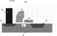
デジタル不揮発性メモリは、周知である。例えば、米国特許第5,029,130号(「’130号特許」)は、スプリットゲート不揮発性メモリセルのアレイを開示し、あらゆる目的のために参照により本明細書に組み込まれる。このようなメモリセルを図2に示す。各メモリセル210は、半導体基板12内に形成され、チャネル領域18をその間に有するソース領域14とドレイン領域16と、を含む。浮遊ゲート20は、チャネル領域18の第1の部分の上方に形成され、チャネル領域18の第1の部分から絶縁されて(かつチャネル領域18の第1の部分導電性を制御して)おり、またソース領域16の一部分の上方に形成される。ワード線端子22(典型的には、ワード線に結合される)は、チャネル領域18の第2の部分の上方に配設され、チャネル領域18の第2の部分から絶縁され、(かつチャネル領域18の第2の部分導電性を制御する)第1の部分と、浮遊ゲート20の上方に、かつ上方でに延在する第2の部分と、を有する。浮遊ゲート20及びワード線端子22は、ゲート酸化物によって基板12から絶縁される。ビット線24はドレイン領域16に結合される。
Digital non-volatile memories are well known. For example, U.S. Pat. No. 5,029,130 ("the '130 patent") discloses an array of split-gate non-volatile memory cells, and is incorporated herein by reference for all purposes. Such a memory cell is shown in FIG. 2. Each
メモリセル210は、ワード線端子22に高圧正電圧を印加することによって消去され(ここで電子は、浮遊ゲートから除去される)、それにより、ファウラーノルドハイムトンネリングによって浮遊ゲート20からワード線端子22まで中間絶縁体を通って浮遊ゲート20の電子をトンネリングさせる。
The
メモリセル210は、ワード線端子22に正電圧、及びソース16に正電圧を印加することによってプログラムされる(ここで電子は、浮遊ゲートに印加される)。電子電流は、ソース16からドレイン14に向かって流れることになる。電子は、ワード線端子22と浮遊ゲート20との間の間隙に達すると、加速し発熱する。熱せられた電子のいくらかは、浮遊ゲート20からの静電引力に起因してゲート酸化物26を通って浮遊ゲート20に注入される。
The
ドレイン14及びワード線端子22に正の読み出し電圧を印加する(ワード線端子下のチャネル領域をターンオンする)ことによって、メモリセル210が読み出される。浮遊ゲート20が正に帯電する(すなわち、電子を消去し、ドレイン16に正に結合する)場合、浮遊ゲート20下のチャネル領域の部分は、次に同様にオンになり、電流は、チャネル領域18を流れ、これは、消去された状態つまり「1」の状態として感知される。浮遊ゲート20が負に帯電する(すなわち、電子でプログラムされる)場合、次に浮遊ゲート20下のチャネル領域の部分は、ほとんど又は完全にオフになり、電流は、チャネル領域18を流れず(又はわずかに流れる)、プログラムされた状態又は「0」の状態として検出される。
The
表1は、読み出し、消去及びプログラム動作を実行するためのメモリセル210の端子に印加され得る典型的な電圧範囲を示す。
表1:図2のフラッシュメモリセル210の動作

Table 1: Operation of the
他のスプリットゲートメモリセル構成が知られている。例えば、図3は、ソース領域14と、ドレイン領域16と、チャネル領域18の第1の部分の上方にある浮遊ゲート20と、チャネル領域18の第2の部分の上方にある選択ゲート28(典型的には、ワード線に結合される)と、浮遊ゲート20の上方にある制御ゲート22と、及びソース領域14の上方にある消去ゲート30と、を備える4ゲートメモリセル310を示す。この構成は、米国特許第6,747,310号に記載され、この米国特許は、あらゆる目的のため参照により本明細書に組み込まれる。ここで、全てのゲートは、浮遊ゲート20を除いて、非浮遊ゲートであり、それらは電圧源に電気的に接続される又は接続可能であることを意味する。プログラミングは、浮遊ゲート20にそれ自体を注入するチャネル領域18からの熱せられた電子によって示される。消去は、浮遊ゲート20から消去ゲート30へトンネリングする電子によって示される。
Other split gate memory cell configurations are known. For example, FIG. 3 shows a
表2は、読み出し、消去及びプログラム動作を実行するためのメモリセル310の端子に印加され得る典型的な電圧範囲を示す。
表2:図3のフラッシュメモリセル310の動作
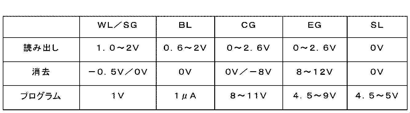
Table 2: Operation of the
図4は、スプリットゲート3ゲートメモリセル410を示す。メモリセル410は、メモリセル410が別個の制御ゲートを有しないことを除いて、図3のメモリセル310と同一である。消去動作(消去ゲートを通しての消去)及び読み出し動作は、制御ゲートバイアスがないことを除いて、図3のものと同様である。プログラミング動作もまた、制御ゲートバイアスなしで行われるため、ソース線のプログラム電圧は、制御ゲートバイアスの不足を補償するためにより高い。
Figure 4 shows a split gate triple
表3は、読み出し、消去及びプログラム動作を実行するためのメモリセル410の端子に印加され得る典型的な電圧範囲を示す。
表3:図4のフラッシュメモリセル410の動作
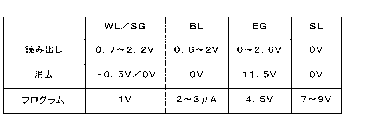
Table 3: Operation of
図5は、積層ゲートメモリセル510を示す。メモリセル510は、浮遊ゲート20がチャネル領域18の上方に延在し、制御ゲート22が絶縁層によって分離された浮遊ゲート20の上方に延在することを除いて、図2のメモリセル210と同様である。消去、プログラミング、及び読み出し動作は、メモリセル210について前述したものと同様の方法で動作する。
Figure 5 shows a stacked
表4は、読み出し、消去及びプログラム動作を実行するためのメモリセル510の端子に印加され得る典型的な電圧範囲を示す。
表4:図5のフラッシュメモリセル510の動作
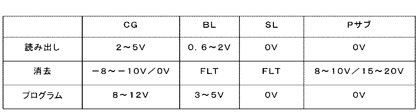
Table 4: Operation of
上記の人工ニューラルネットワークにおける不揮発性メモリセルのタイプのうちの1つを含むメモリアレイを利用するために、2つの修正が行われる。第1に、以下に更に説明されるように、アレイ内の他のメモリセルのメモリ状態に悪影響を与えずに各メモリセルを個々にプログラム、消去、及び読み出しすることができるように線を構成する。第2に、メモリセルの連続(アナログ)プログラミングを提供する。 To utilize a memory array containing one of the types of non-volatile memory cells in the artificial neural network described above, two modifications are made. First, as further described below, the lines are configured so that each memory cell can be individually programmed, erased, and read without adversely affecting the memory state of other memory cells in the array. Second, provide for continuous (analog) programming of the memory cells.
具体的には、アレイ内の各メモリセルのメモリ状態(すなわち、浮遊ゲートの電荷)を、完全に消去された状態から完全にプログラムされた状態へ、独立して、かつ他のメモリセルの異常が最小で連続的に変更することができる。別の実施形態において、アレイ内の各メモリセルのメモリ状態(すなわち、浮遊ゲートの電荷)を、完全にプログラムされた状態から完全に消去された状態へ、及び逆もまた同様に、独立して、かつ他のメモリセルの異常が最小で連続的に変更することができる。このことは、セル記憶がアナログであるか、又は多数の別個の値(16又は64の異なる値など)のうちの1つを最低限記憶することができ、それは、メモリアレイ内の全てのセルの非常に正確、かつ個々の調整を可能にし、またメモリアレイを記憶に対して理想的にし、ニューラルネットワークのシナプシスの重みに微調整を加えることを意味する。
不揮発性メモリセルアレイを使用するニューラルネットワーク
Specifically, the memory state (i.e., the charge on the floating gate) of each memory cell in the array can be changed from a fully erased state to a fully programmed state, independently and continuously with minimal disturbance to other memory cells. In another embodiment, the memory state (i.e., the charge on the floating gate) of each memory cell in the array can be changed from a fully programmed state to a fully erased state, and vice versa, independently and continuously with minimal disturbance to other memory cells. This means that the cell storage is analog, or can at a minimum store one of many distinct values (such as 16 or 64 different values), which allows for very precise and individual tuning of every cell in the memory array, and makes the memory array ideal for storing and fine-tuning the synaptic weights of a neural network.
Neural network using non-volatile memory cell arrays
図6は、不揮発性メモリアレイを利用するニューラルネットワークの非限定実施例を概念的に示す。この例は、顔認識アプリケーションのために不揮発性メモリアレイニューラルネットを使用するが、不揮発性メモリアレイベースのニューラルネットワークを使用して他の任意の適切なアプリケーションを実施することができる。 Figure 6 conceptually illustrates a non-limiting example of a neural network utilizing a non-volatile memory array. This example uses a non-volatile memory array neural net for a face recognition application, although any other suitable application can be implemented using a non-volatile memory array-based neural network.
S0は入力であり、この例では、5ビット精度の32×32ピクセルRGB画像である(すなわち、各色R、G、及びBにつき1つずつの3つの32×32ピクセルアレイ、各ピクセルが5ビット精度である)。S0からC1に行くシナプスCB1は、異なる重みのセット及び共有される重みの両方を有し、入力画像を3×3ピクセルの重なり合うフィルタでスキャンし(カーネル)、1ピクセル(又はモデルによって決まるように2ピクセル以上)ずつフィルタをシフトする。具体的には、画像の3×3部分における9ピクセルの値(すなわち、フィルタ又はカーネルと呼ばれる)は、シナプスCB1に提供され、それによってこれらの9個の入力値に適切な重みを乗じ、その乗算の出力の合計後、単一の出力値が決定され、特徴マップC1の層の1つのピクセルを生成するためにCB1の第1のニューロンによって与えられる。3×3フィルタは次に右側に1ピクセルだけシフトされ(すなわち、3ピクセルの列を右側に追加し、左側で3ピクセルの列をドロップする)、そのため、この新しく位置づけられたフィルタの9ピクセル値が、シナプスCB1に提供されるため、それらに同じ重みを乗じ、関連するニューロンによって第2の単一の出力値を決定する。このプロセスを、3×3フィルタが32×32ピクセル画像全体にわたって3色全て及び全てのビットについてスキャンするまで続ける(精度値)。プロセスは次に、層C1の特徴マップ全てが計算されるまで、異なる重みのセットを使用して繰り返されて、C1の異なる特徴マップを生成する。 S0 is the input, which in this example is a 32x32 pixel RGB image with 5-bit precision (i.e., three 32x32 pixel arrays, one for each color R, G, and B, each pixel with 5-bit precision). The synapse CB1 going from S0 to C1 has both a set of distinct and shared weights, scans the input image with overlapping filters of 3x3 pixels (kernels), and shifts the filters by one pixel (or more than one pixel, as determined by the model). Specifically, the values of the 9 pixels in the 3x3 portion of the image (i.e., called filters or kernels) are provided to the synapse CB1, which multiplies these 9 input values by the appropriate weights, and after summing the outputs of the multiplication, a single output value is determined and given by the first neuron of CB1 to generate one pixel of the layer of feature map C1. The 3x3 filter is then shifted one pixel to the right (i.e., add a column of 3 pixels to the right and drop a column of 3 pixels on the left) so that the 9 pixel values of this newly positioned filter are provided to synapse CB1, which multiplies them by the same weights to determine a second single output value by the associated neuron. This process continues until the 3x3 filter has scanned the entire 32x32 pixel image for all three colors and all bits (precision value). The process is then repeated using different sets of weights to generate different feature maps of C1 until all feature maps of layer C1 have been calculated.
C1において、本例では、それぞれ30×30ピクセルを有する16個の特徴マップが存在する。各ピクセルは、入力とカーネルとの乗算から抽出された新しい特徴ピクセルであり、したがって、各特徴マップは、2次元アレイであり、したがってこの例では、シナプスCB1は、2次元アレイの16層を構成する(本明細書で言及されるニューロン層及びアレイは、必ずしも物理的関係ではなく論理的な関係であり、すなわち、アレイは必ずしも物理的な2次元アレイに配向されないことに留意する)。16個の特徴マップのそれぞれは、フィルタスキャンに適用される16個の異なるシナプス重みのセットの1つによって生成される。C1特徴マップは全て、境界同定など同じ画像特徴の異なる態様を対象とすることができる。例えば、第1のマップ(この第1のマップを生成するのに使用される全てのスキャンに共有される第1の重みセットを使用して生成される)は、円形エッジを識別することができ、第2のマップ(第1の重みセットと異なる第2の重みセットを使用して生成される)は、方形エッジ又は特定の特徴のアスペクト比などを識別することができる。 In C1, in this example, there are 16 feature maps, each with 30x30 pixels. Each pixel is a new feature pixel extracted from the multiplication of the input with the kernel, and therefore each feature map is a two-dimensional array, and thus in this example, the synapses CB1 constitute 16 layers of two-dimensional arrays (note that the neuron layers and arrays referred to herein are logical, not necessarily physical, relationships, i.e., the arrays are not necessarily oriented in a physical two-dimensional array). Each of the 16 feature maps is generated by one of 16 different sets of synaptic weights applied to the filter scans. The C1 feature maps can all target different aspects of the same image feature, such as boundary identification. For example, a first map (generated using a first set of weights shared by all scans used to generate this first map) can identify circular edges, a second map (generated using a second set of weights different from the first set of weights) can identify square edges or the aspect ratio of a particular feature, etc.
活性化関数P1(プーリング)は、C1からS1へ行く前に適用され、各特徴マップ中の連続する、重なり合わない2×2領域からの値をプールする。プーリング段階の目的は、平均して近隣の位置にすること(又はmax関数もまた使用され得る)、例えばエッジ位置の依存を低減すること、及び次の段階に行く前にデータサイズを低減することである。S1において、16個の15×15特徴マップ(すなわち、16個のそれぞれ15×15ピクセルの異なるアレイ)が存在する。S1からC2へ行くCB2内のシナプス及び関連するニューロンは、S1内のマップを1ピクセルのフィルタシフトを使用して4×4フィルタでスキャンする。C2において、22個の12×12特徴マップが存在する。活性化関数P2(プーリング)は、C2からS2へ行く前に適用され、各特徴マップ中の連続する、重なり合わない2×2領域からの値をプールする。S2において、22個の6×6特徴マップが存在する。活性化関数は、S2からC3へ行くシナプスCB3で適用され、ここでC3内の全てのニューロンはS2内の全てのマップに接続する。C3において、64個のニューロンが存在する。C3から出力S3へ行くシナプスCB4は、S3をC3と完全に接続する。S3における出力は、10個のニューロンを含み、ここで最も高い出力ニューロンは、クラスを決定する。この出力は、例えば、元の画像の内容の同定又は分類を示すことができる。 Activation function P1 (pooling) is applied before going from C1 to S1 to pool values from consecutive, non-overlapping 2x2 regions in each feature map. The purpose of the pooling stage is to average to nearby locations (or a max function can also be used), e.g. to reduce edge location dependency, and to reduce data size before going to the next stage. In S1, there are 16 15x15 feature maps (i.e. 16 different arrays of 15x15 pixels each). The synapses and associated neurons in CB2 going from S1 to C2 scan the maps in S1 with a 4x4 filter using a filter shift of 1 pixel. In C2, there are 22 12x12 feature maps. Activation function P2 (pooling) is applied before going from C2 to S2 to pool values from consecutive, non-overlapping 2x2 regions in each feature map. In S2, there are 22 6x6 feature maps. The activation function is applied at synapse CB3 going from S2 to C3, where all neurons in C3 connect to all maps in S2. There are 64 neurons in C3. Synapse CB4 going from C3 to output S3 fully connects S3 with C3. The output at S3 contains 10 neurons, where the highest output neuron determines the class. This output can indicate, for example, an identification or classification of the content of the original image.
シナプスの各レベルは、不揮発性メモリセルのアレイ又はアレイの一部を使用して実行される。図7は、不揮発性メモリセルを含み、入力層と次の層との間のシナプスとして利用されるベクトルマトリクス乗算(VMM)アレイのブロック図である。具体的には、VMM32は、不揮発性メモリセルのアレイ33、消去ゲート及びワード線ゲートデコーダ34、制御ゲートデコーダ35、ビット線デコーダ36、並びにソース線デコーダ37を含み、それらのデコーダはメモリアレイ33に対する入力をデコードする。この例におけるソース線デコーダ37はまた、メモリセルアレイの出力をデコードする。あるいは、ビット線デコーダ36は、メモリアレイの出力をデコードすることができる。メモリアレイは、2つの目的を果たす。第1に、VMMにより使用される重みを記憶する。第2に、メモリアレイは、効果的に、入力に、メモリアレイに記憶された重みを乗じ、それを出力線(ソース線またはビット線)ごとに加算して出力を生成し、これは、次の層への入力又は最後の層への入力になる。乗算及び加算関数を実行することによって、メモリアレイは、別個の乗算及び加算論理回路の必要性をなくし、また、その場でのメモリ計算のために電力効率も良い。
Each level of synapses is implemented using an array or a portion of an array of non-volatile memory cells. FIG. 7 is a block diagram of a vector matrix multiplication (VMM) array that includes non-volatile memory cells and is used as a synapse between an input layer and the next layer. Specifically, the
メモリアレイの出力は差動加算器(加算オペアンプなど)38に供給され、差動加算器はメモリセルアレイの出力を合計してその畳み込み用の単一の値を生成する。差動加算器は、正の入力で正の重みと負の重みとの合計を実現するようなものである。合計された出力値は、次に出力を整流する活性化関数回路39に供給される。活性化関数には、シグモイド、tanh、又はReLU関数が含まれ得る。整流された出力値は、次の層(例えば上の説明ではC1)として特徴マップの要素になり、次いで、次のシナプスに適用されて次の特徴マップ層又は最後の層を生成する。したがって、この例では、メモリアレイは、複数のシナプスを構成し(ニューロンの前の層から、又は画像データベースなどの入力層から入力を受信する)、加算オペアンプ38及び活性化関数回路39は、複数のニューロンを構成する。
The output of the memory array is fed to a differential adder (such as a summing op-amp) 38, which sums the outputs of the memory cell array to generate a single value for the convolution. The differential adder is such that a positive input realizes the sum of positive and negative weights. The summed output value is then fed to an
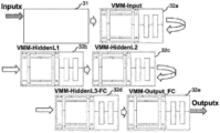
図8は、様々なレベルのVMMのブロック図である。図14に示されるように、入力は、デジタルアナログ変換器31によってデジタルからアナログに変換され、入力VMM32aに提供される。入力VMM32aによって生成された出力は、次のVMM(隠しレベル1)32bへの入力として提供され、VMM(隠しレベル1)32bは、同様にして、次のVMM(隠しレベル2)32bへの入力として提供される出力を生成する、出力を生成する、などとなる。VMMの32の様々な層は、畳み込みニューラルネットワーク(convolutional neural network、CNN)のシナプス及びニューロンの異なる層として機能する。各VMMは、スタンドアローンの不揮発性メモリアレイであり得、又は複数のVMMは、同じ不揮発性メモリアレイの異なる部分を利用することができ、又は複数のVMMは、同じ不揮発性メモリアレイの重なり合う部分を利用することができる。図8に示される例は、5つの層(32a、32b、32c、32d、32e):1つの入力層(32a)、2つの隠れ層(32b、32c)、及び2つの完全に接続された層(32d、32e)を含む。当業者であれば、これは単なる例示であり、代わりにシステムが2つを超える隠れ層及び2つを超える完全に接続された層を備え得ることを理解するであろう。
ベクトルマトリクス乗算(VMM)アレイ
FIG. 8 is a block diagram of the various levels of VMMs. As shown in FIG. 14, the input is converted from digital to analog by a digital-to-
Vector Matrix Multiplication (VMM) Array
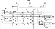
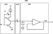
図9は、図2に示されるタイプのメモリセルに特に適したニューロンVMM900を示し、入力層と次の層との間のシナプス及びニューロンの一部として利用される。VMM900は、不揮発性メモリセルのメモリアレイ903、基準アレイ901、及び基準アレイ902を備える。基準アレイ901及び902は、端子BLR0~3内に流れ込む電流入力を電圧入力WL0~3に変換する役割を果たす。図示の基準アレイ901及び902は、列方向にある。一般に、基準アレイ方向は入力線に直交する。実際には、基準メモリセルは、マルチプレクサ(1つのマルチプレクサ及び基準ビット線をバイアスするための1つのカスコードトランジスタVBLRを含むマルチプレクサ914)を介して接続されたダイオードであり、電流入力はそれらのに流れ込む。基準セルは、標的基準レベルに調整される。
Figure 9 shows a neuron VMM 900 that is particularly suited for memory cells of the type shown in Figure 2, used as part of synapses and neurons between an input layer and the next layer. The VMM 900 comprises a
メモリアレイ903は、2つの目的を果たす。第1に、VMM900により使用される重みを記憶する。第2に、メモリアレイ903は、入力(端子BLR0~3に提供される電流入力であって、基準アレイ901及び902がこれらの電流入力を入力電圧に変換してワード線WL0~3に供給する)にメモリアレイに記憶された重みを有効に乗算して、出力を生成し、これは次の層への入力又は最終の層への入力となる。乗算関数を実行することによって、メモリアレイは、別個の乗算論理回路の必要性をなくし、また電力効率も良い。ここで、電圧入力はワード線に提供され、出力は読み出し(推論)動作中にビット線に現れる。ビット線の電流は、ビット線に接続されたメモリセルからの全ての電流の合計関数を実行する。
The
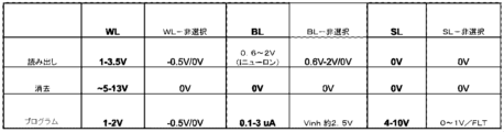
図42は、VMM900の動作電圧を示す。表中の列は、選択セルのワード線、非選択セルのワード線、選択セルのビット線、非選択セルのビット線、選択セルのソース線、及び非選択セルのソース線に印加された電圧を示す。行は、読み出し、消去、及びプログラムの動作を示す。 Figure 42 shows the operating voltages of the VMM900. The columns in the table show the voltages applied to the word line of the selected cell, the word lines of the unselected cells, the bit lines of the selected cell, the bit lines of the unselected cells, the source line of the selected cell, and the source lines of the unselected cells. The rows show the read, erase, and program operations.
図10は、図2に示されるタイプのメモリセルに特に適したニューロンVMM1000を示し、入力層と次の層との間のシナプス及びニューロンの一部として利用される。VMM1000は、不揮発性メモリセルのメモリアレイ1003、基準アレイ1001、及び基準アレイ1002を備える。VMM1000は、VMM1000においてワード線が垂直方向に延びることを除いて、VMM900と同様である。2つの基準アレイ1001(頂部で、偶数行の電圧への基準変換入力電流を提供する)及び1002(底部で、奇数行の電圧への基準変換入力電流を提供する)が存在する。ここで、入力はワード線に提供され、出力は読み出し動作中にソース線に現れる。ソース線の電流は、ソース線に接続されたメモリセルからの全ての電流の合計関数を実行する。
Figure 10 shows a neuron VMM1000 that is particularly suited for memory cells of the type shown in Figure 2, which are used as part of synapses and neurons between an input layer and the next layer. VMM1000 comprises a
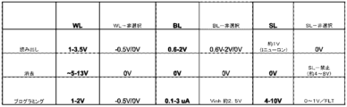
図43は、VMM1000の動作電圧を示す。表中の列は、選択セルのワード線、非選択セルのワード線、選択セルのビット線、非選択セルのビット線、選択セルのソース線、及び非選択セルのソース線に印加された電圧を示す。行は、読み出し、消去、及びプログラムの動作を示す。 Figure 43 shows the operating voltages of the VMM1000. The columns in the table show the voltages applied to the word line of the selected cell, the word lines of the unselected cells, the bit lines of the selected cell, the bit lines of the unselected cells, the source line of the selected cell, and the source lines of the unselected cells. The rows show the read, erase, and program operations.
図11は、図3に示されるタイプのメモリセルに特に適したニューロンVMM1100を示し、入力層と次の層との間のシナプス及びニューロンの一部として利用される。VMM1100は、不揮発性メモリセルのメモリアレイ1101、基準アレイ1102(偶数行の入力電圧への基準変換入力電流を提供する)、及び基準アレイ1103(奇数行の入力電圧への基準変換入力電流を提供する)を備える。VMM1100は、VMM1100を除きVMM900と同様である。VMM1100は、メモリセルの行の制御ゲートに結合された制御線1106、及びメモリセルの隣接する行の消去ゲートに結合された制御線1107を更に備える。ここで、ワード線、制御ゲート線、消去ゲート線は同じ方向である。VMMは、選択された基準メモリセル及びスイッチ1105(mux 1114の一部)のビット線コンタクトに選択的に結合する基準ビット線選択トランジスタ1104(mux 1114の一部)を更に備え、このビット線選択トランジスタ1104は、特定の選択された基準メモリセルのために、基準ビット線を制御線1106に選択的に結合する。ここで、入力は(メモリアレイ1101の)ワード線に提供され、出力は読み出し動作中にビット線1109などのビット線に現れる。ビット線の電流は、ビット線に接続されたメモリセルからの全ての電流の合計関数を実行する。
Figure 11 shows a neuron VMM1100 that is particularly suited for memory cells of the type shown in Figure 3, which are used as part of synapses and neurons between the input layer and the next layer. VMM1100 comprises a
図44は、VMM1100の動作電圧を示す。表中の列は、選択セルのワード線、非選択セルのワード線、選択セルのビット線、非選択セルのビット線、選択セルの制御ゲート、選択セルと同じセクタ内の非選択セルの制御ゲート、選択セルとは異なるセクタ内の非選択セルの制御ゲート、選択セルの消去ゲート、非選択セルの消去ゲート、選択セルのソース線、及び非選択セルのソース線の電圧を示す。行は、読み出し、消去、及びプログラムの動作を示す。 Figure 44 shows the operating voltages of VMM1100. The columns in the table show the voltages of the word line of the selected cell, the word lines of the unselected cells, the bit line of the selected cell, the bit lines of the unselected cells, the control gate of the selected cell, the control gate of the unselected cells in the same sector as the selected cell, the control gate of the unselected cells in a different sector than the selected cell, the erase gate of the selected cell, the erase gate of the unselected cells, the source line of the selected cell, and the source line of the unselected cells. The rows show the read, erase, and program operations.
図12は、図3に示されるタイプのメモリセルに特に適したニューロンVMM1200を示し、入力層と次の層との間のシナプス及びニューロンの一部として利用される。VMM1200は、VMM1200で、消去ゲート線1201などの消去ゲート線が垂直方向に延びることを除いて、VMM1100と同様である。ここで、入力はワード線に提供され、出力はソース線に現れる。ビット線の電流は、ビット線に接続されたメモリセルからの全ての電流の合計関数を実行する。
Figure 12 shows a neuron VMM1200 that is particularly suited for memory cells of the type shown in Figure 3, used as part of a neuron and synapse between an input layer and the next layer. VMM1200 is similar to VMM1100, except that in VMM1200, the erase gate lines, such as erase
図45は、VMM1200の動作電圧を示す。表中の列は、選択セルのワード線、非選択セルのワード線、選択セルのビット線、非選択セルのビット線、選択セルの制御ゲート、選択セルと同じセクタ内の非選択セルの制御ゲート、選択セルとは異なるセクタ内の非選択セルの制御ゲート、選択セルの消去ゲート、非選択セルの消去ゲート、選択セルのソース線、及び非選択セルのソース線の電圧を示す。行は、読み出し、消去、及びプログラムの動作を示す。 Figure 45 shows the operating voltages of the VMM1200. The columns in the table show the voltages of the word line of the selected cell, the word lines of the unselected cells, the bit line of the selected cell, the bit lines of the unselected cells, the control gate of the selected cell, the control gates of the unselected cells in the same sector as the selected cell, the control gates of the unselected cells in a different sector than the selected cell, the erase gate of the selected cell, the erase gates of the unselected cells, the source line of the selected cell, and the source lines of the unselected cells. The rows show the read, erase, and program operations.
図13は、図3に示されるタイプのメモリセルに特に適したニューロンVMM1300を示し、入力層と次の層との間のシナプス及びニューロンの一部として利用される。VMM1300は、不揮発性メモリセルのメモリアレイ1301、及び基準アレイ1302(アレイの頂部で)を備える。あるいは、別の基準アレイが、図10のものと同様に、底部に位置することができる。他の点では、VMM1300は、VMM1300で、制御ゲート線1303などの制御ゲート線が垂直方向に延び(したがって、行方向の基準アレイ1302が入力制御ゲート線に直交する)、消去ゲート線1304などの消去ゲート線が水平方向に延びることを除いて、VMM1200と同様である。ここで、入力は制御ゲート線に提供され、出力はソース線に現れる。一実施形態では、偶数行のみが使用され、別の実施形態では、奇数行のみが使用される。ソース線の電流は、ソース線に接続されたメモリセルからの全ての電流の合計関数を実行する。
13 shows a neuron VMM1300 that is particularly suited for memory cells of the type shown in FIG. 3, which are utilized as part of synapses and neurons between an input layer and the next layer. VMM1300 comprises a
ニューラルネットワークについて本明細書に記載されるように、フラッシュセルは、サブ閾値領域で動作するように構成されることが好ましい。 As described herein for neural networks, the flash cells are preferably configured to operate in the sub-threshold region.
本明細書に記載されたメモリセルは、弱反転にバイアスされる。
Ids=Io*e(Vg-Vth)/kVt=w*Io*e(Vg)/kVt
w=e(-Vth)/kVt
The memory cells described herein are biased in weak inversion.
Ids=Io * e (Vg-Vth)/kVt = w * Io * e (Vg)/kVt
w = e (-Vth)/kVt
入力電流を入力電圧に変換するためにメモリセルを使用するIーVログ変換器について:
Vg=k*Vt*log[Ids/wp*Io]
For an I-V log converter that uses memory cells to convert an input current to an input voltage:
Vg=k * Vt * log[Ids/wp * Io]
ベクトルマトリクス乗算器VMMとして使用されるメモリアレイについて、出力電流は以下である:
Iout=wa*Io*e(Vg)/kVt、すなわち
Iout=(wa/wp)*Iin=W*Iin
W=e(Vthp-Vtha)/kVt
For a memory array used as a vector matrix multiplier VMM, the output current is:
Iout = wa * Io * e (Vg)/kVt , i.e. Iout = (wa/wp) * Iin = W * Iin
W = e (Vthp-Vtha)/kVt
ワード線又は制御ゲートは、入力電圧に対するメモリセルの入力として使用することができる。 The word line or control gate can be used as the input of the memory cell for an input voltage.
あるいは、フラッシュメモリセルは、線形領域で動作するように構成することができる。
Ids=β*(Vgs-Vth)*Vds;β=u*Cox*W/L
W α(Vgs-Vth)
Alternatively, the flash memory cells can be configured to operate in the linear region.
Ids=β * (Vgs-Vth) * Vds;β=u * Cox * W/L
W α(Vgs-Vth)
I-V線形変換器では、線形領域で動作するメモリセルを使用して、入力/出力電流を入力/出力電圧に線形に変換することができる。 In an I-V linear converter, input/output currents can be linearly converted to input/output voltages using memory cells operating in the linear region.
ESFベクトルマトリクス乗算器の他の実施形態は、参照により本明細書に組み込まれる米国特許出願第15/826,345号に記載されているとおりである。ソース線又はビット線は、ニューロン出力(電流和出力)として使用することができる。 Other embodiments of the ESF vector matrix multiplier are described in U.S. Patent Application No. 15/826,345, which is incorporated herein by reference. The source lines or bit lines can be used as neuron outputs (current sum outputs).
図14は、ビット線デコーダ回路1400の一実施形態を示す。ビット線デコーダ回路1400は、列デコーダ1402及びアナログニューロモーフィックニューロン(「ANN」)列デコーダ1403を備え、これらの各々はVMMアレイ1401に結合される。VMMアレイは、先に論じたVMM設計(VMM900、1000、1100、1200、及び1300など)又は他のVMM設計のうちのいずれかに基づくことができる。
Figure 14 illustrates one embodiment of a bit
アナログニューロモーフィックシステムによる1つの課題は、システムが(読み出し動作を伴う)プログラム及び検証を行うことができなければならず、アレイ内の全てのセルが選択され読み出されるANN読み出しを実行することができなければならないことである。換言すれば、ビット線デコーダは、場合によっては1つのビット線のみを選択しなければならならず、他の例では全てのビット線を選択しなければならない。 One challenge with analog neuromorphic systems is that the system must be able to program and verify (which involves a read operation) and perform ANN reads where every cell in the array is selected and read. In other words, the bit line decoder must select only one bit line in some cases and all bit lines in other cases.
ビット線デコーダ回路1400は、この目的を達成する。列デコーダ1402は、従来の列デコーダ(プログラム及び消去、又はPE、デコード経路)であり、プログラム及びプログラム検証(感知動作)などの個々のビット線を選択するために使用することができる。列デコーダ1402の出力は、プログラム、PE検証、及び消去を制御するためのプログラム/消去(PE)列ドライバ回路に結合される(図14には示されていない)。ANN列デコーダ1403は、一度に全てのビット線での読み出し動作を可能にするように具体的に設計された列デコーダである。ANN列デコーダ1403は、ビット線(ここではBL0)に結合された例示的な選択トランジスタ1405及び出力回路(例えば、tanh、シグモイド、ReLUなどの電流加算器及び活性化関数)1406を備える。同じデバイスのセットが、他のビット線の各々に取り付けられる。選択トランジスタ1405などの選択トランジスタの全ては、選択線1404に結合される。ANN読み出し動作中、選択線1404が有効にされ、選択トランジスタ1405などの選択トランジスタの各々がオンになり、次いで、各ビット線からの電流が回路1406及び出力などの出力回路によって受信される。
The bit
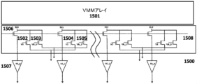
図15は、ビット線デコーダ回路1500の一実施形態を示す。ビット線デコーダ回路1500は、VMMアレイ1501に結合される。VMMアレイは、先に論じたVMM設計(VMM900、1000、1100、1200、及び1300など)又は他のVMM設計のうちのいずれかに基づくことができる。
Figure 15 illustrates one embodiment of a bit
選択トランジスタ1502及び1503は、一対の相補的制御信号(V0及びVB_0)によって制御され、ビット線(BL0)に結合される。選択トランジスタ1504及び1505は、別の対の相補的制御信号(V1及びVB_1)によって制御され、別のビット線(BL1)に結合される。選択トランジスタ1502及び1504は、プログラミングを有効にするために同じ出力に結合され、選択トランジスタ1503及び1505は、禁止プログラミングのためなどの同じ出力に結合される。トランジスタ1502/1503/1504/1505の出力線(プログラム及び消去PEデコード経路)は、プログラム、PE検証、及び消去(図示せず)を制御するためのPE列ドライバ回路に結合されるようなものである。
選択トランジスタ1506は、ビット線(BL0)に結合され、出力及び活性化関数回路1507(例えば、tanh、シグモイド、ReLUなどの電流加算及び活性化関数)に結合される。選択トランジスタ1506は制御線1508によって制御される。
BL0のみが活性化されると、制御線1508はデアサートされ、信号V0はアサートされ、したがってBL0のみを読み取る。ANN読み出し動作中に、制御線1508がアサートされ、選択トランジスタ1506及び同様のトランジスタがオンにされ、全てのビット線は、全てのニューロン処理のために読み出される。
When only BL0 is activated,
図16は、ビット線デコーダ回路1600の一実施形態を示す。ビット線デコーダ回路1600は、VMMアレイ1601に結合される。VMMアレイは、先に論じたVMM設計(VMM900、1000、1100、1200、及び1300など)又は他のVMM設計のうちのいずれかに基づくことができる。
Figure 16 illustrates one embodiment of a bit
選択トランジスタ1601は、ビット線(BL0)に結合され、出力及び活性化関数回路1603に結合される。選択トランジスタ1602は、ビット線(BL0)及び共通出力(PEデコード経路)に結合される。
BL0のみが活性化されると、選択トランジスタ1602が活性化され、BL0が共通出力に取り付けられる。ANN読み出し動作中、選択トランジスタ1601及び同様のトランジスタがオンにされ、全てのビット線が読み出される。
When only BL0 is activated,
図14、15及び16のデコードに関して、非選択トランジスタについては、トランジスタ漏れがメモリセル性能に影響を及ぼすことを低減するために、負バイアスを与えることができる。あるいは、アレイがANN動作中である間に、PEデコード経路に負バイアスを与えることができる。負バイアスは、-0.1V~-0.5V以上であり得る。 For the decode of Figures 14, 15 and 16, the unselected transistors can be negatively biased to reduce transistor leakage from affecting memory cell performance. Alternatively, the PE decode path can be negatively biased while the array is in ANN operation. The negative bias can be -0.1V to -0.5V or higher.
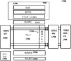
図17は、VMN1700を示す。VMMシステム1700は、VMMアレイ1701及び基準アレイ1720(これは、VMM900、1000、1100、1200、及び1300、又は他のVMM設計など、前述のVMM設計のいずれかに基づくことができる)、低電圧行デコーダ1702、高電圧行デコーダ1703、参照セル低電圧列デコーダ1704(列方向の基準アレイのために示され、行方向に変換を出力するための入力を提供することを意味する)、ビット線PEドライバ1712、ビット線マルチプレクサ1706、活性化関数回路及び加算器1707、制御論理1705、及びアナログバイアス回路1708を備える。
Figure 17 shows a
図示のように、基準セル低電圧列デコーダ1704は、列方向の基準アレイ1720のためにあり、行方向に変換を出力するための入力を提供することを意味する。基準アレイが行方向にある場合、基準デコーダは、アレイの頂部及び/又は底部で行われ、列方向に変換を出力するための入力を提供する必要がある。
As shown, the reference cell low
低電圧行デコーダ1702は、読み出し及びプログラム動作のためのバイアス電圧を提供し、高電圧行デコーダ1703のデコード信号を提供する。高電圧行デコーダ1703は、プログラム及び消去動作のための高電圧バイアス信号を提供する。参照セル低電圧列デコーダ1704は、参照セルのデコード関数を提供する。ビット線PEドライバ1712は、プログラム、検証、及び消去におけるビット線の制御関数を提供する。バイアス回路1705は、様々なプログラム、消去、プログラム検証、及び読み出し動作に必要な複数の電圧を提供する共有バイアスブロックである。
The low
図18は、VMMシステム1800を示す。VMMシステム1800は、VMMシステム1800が、赤色アレイ1801、ビット線PEドライバBLDRV1802、高電圧列デコーダ1803、NVRセクタ1804、及び基準アレイ1820を更に備えることを除いて、VMMシステム1700と同様である。高電圧列デコーダ1803は、垂直デコード線の高電圧バイアスを提供する。赤色アレイ1802は、欠陥のあるアレイ部分を置き換えるためのアレイ冗長性を提供する。NVR(不揮発性レジスタ別名情報セクタ)セクタ1804は、ユーザ情報、デバイスID、パスワード、セキュリティキー、トリムビット、構成ビット、製造情報などを記憶するために使用されるアレイセクタであるセクタである。
Figure 18 shows a
図19は、VMMシステム1900を示す。VMMシステム1900は、VMMシステム1900が参照システム1999を更に備えることを除いて、VMMシステム1800と同様である。基準システム1999は、基準アレイ1901、基準アレイ低電圧行デコーダ1902、基準アレイ高電圧行デコーダ1903、及び基準アレイ低電圧列デコーダ1904を備える。基準システムは、複数のVMMシステムにわたって共有することができる。VMMシステムは、NVRセクタ1905を更に備える。
Figure 19 shows a
基準アレイ低電圧行デコーダ1902は、基準アレイ1901を伴う読み出し及びプログラミング動作のためのバイアス電圧を提供し、基準アレイ高電圧行デコーダ1903のデコード信号も提供する。基準アレイ高電圧行デコーダ1903は、基準アレイ1901を伴うプログラム及び動作のための高電圧バイアスを提供する。基準アレイ低電圧列デコーダ1904は、基準アレイ1901のデコード関数を提供する。基準アレイ1901は、プログラム検証のための基準ターゲット又はセルマージンを提供する(辺縁セルを探索する)ようなものである。
The reference array low
図20は、ワード線ドライバ2000を示す。ワード線ドライバ2000は、ワード線(本明細書に示される例示的なワード線WL0、WL1、WL2、及びWL3など)を選択し、そのワード線にバイアス電圧を提供する。各ワード線は、制御線2001によって制御される選択iso(絶縁)トランジスタ2002などの選択トランジスタに取り付けられる。isoトランジスタ2002は、ワード線デコードトランジスタから消去(例えば、8~12V)などの高電圧を絶縁するために使用され、これはIOトランジスタ(例えば、1.8V、3.3V)で実装することができる。ここで、任意の動作中に、制御線2001が活性化され、isoトランジスタ2002を選択するのに類似した全ての選択トランジスタがオンにされる。例示的バイアストランジスタ2003(ワード線デコード回路の一部)は、ワード線を第1のバイアス電圧(3Vなど)に選択的に結合させ、例示的なバイアストランジスタ2004(ワード線デコード回路の一部)は、ワード線を第2のバイアス電圧(第1のバイアス電圧より低く、接地を含み、間のバイアスであり、非使用メモリ行からの漏れを低減するための負電圧バイアスである)に選択的に結合させた。ANN読み出し動作中、全ての使用ワード線が選択され、第1のバイアス電圧に結び付けられる。全ての非使用ワード線は、第2のバイアス電圧に結び付けられる。プログラム動作などの他の動作中に、一方のワード線のみが選択され、他方のワード線が第2のバイアス電圧に結び付けられるまで選択され、これは、アレイ漏れを低減するために負バイアス(例えば、-0.3~-0.5V以上)であり得る。
20 shows a
図21は、ワード線ドライバ2100を示す。ワード線ドライバ2100は、バイアストランジスタ2103などの頂部トランジスタがバイアス電圧に個別に結合され得ることを除いて、ワード線ドライバ2000と同様であり、このようなトランジスタは全てワード線ドライバ2000内のように共に結び付けられない。これにより、全てのワード線は、同時に異なる独立した電圧を同時に有することが可能になる。
Figure 21 shows
図22は、ワード線ドライバ2200を示す。ワード線ドライバ2200は、バイアストランジスタ2103及び2104がデコーダ回路2201及びインバータ2202に結合されることを除いて、ワード線ドライバ2100と同様である。したがって、図22は、ワード線ドライバ2200内のデコードサブ回路2203を示す。
Figure 22 shows
図23は、ワード線ドライバ2300を示す。ワード線ドライバ2300は、バイアストランジスタ2103及び2104がシフトレジスタ2301のステージ2302の出力に結合されることを除いて、ワード線ドライバ2100と同様である。シフトレジスタ1301は、データのシリアルシフト(レジスタをシリアル計時する)によって、データパターンのシフトに応じて1つ以上の行が同時に有効になることを可能にするなど、各列を独立して制御することを可能にする。
Figure 23 shows
図24は、ワード線ドライバ2400を示す。ワード線ドライバ2400は、各選択トランジスタがコンデンサ2403などのコンデンサに更に結合されることを除いて、ワード線ドライバ2000と同様である。コンデンサ2403は、トランジスタ2401によって線2440の電圧をサンプリングするためにトランジスタ2401によって有効にされた、動作の開始時のワード線にプリチャージ又はバイアスを提供することができる。コンデンサ2403は、各ワード線に対する入力電圧をサンプリング及び保持するように作用する(S/H)。トランジスタ2401は、VMMアレイのANN動作(アレイ電流加算器及び活性化関数)中にオフであり、S/Hコンデンサの電圧がワード線の(浮遊)電圧源として機能することを意味する。あるいは、コンデンサ2403は、メモリアレイからのワード線容量によって提供され得る。
Figure 24 shows
図25は、ワード線ドライバ2500を示す。ワード線ドライバ2500は、バイアストランジスタ2501及び2502がそれぞれスイッチ2503及び2504に接続されることを除いて、前述のワード線ドライバと同様である。スイッチ2503は、opa(演算増幅器)2505及びスイッチ2504の出力を受信し、スイッチ2504は、opa2505の負入力に基準入力を提供し、これにより、opa2505、トランジスタ2501、スイッチ2503及び2504によって提供された閉ループの作用により、コンデンサ2403によって記憶された電圧を本質的に提供する。このようにして、スイッチ2503及び2504が閉じられると、入力2506の電圧がトランジスタ2501によってコンデンサ2403に重畳される。あるいは、コンデンサ2403は、メモリアレイからのワード線容量によって提供され得る。
Figure 25 shows a
図26は、ワード線ドライバを示す。ワード線ドライバ2600は、電圧をワード線WL0に駆動するためにコンデンサ2604の電圧の電圧バッファとして作用する増幅器2601の追加を除いて、前述したワード線ドライバと同様であり、S/Hコンデンサの電圧がワード線のための(浮遊)電圧源として機能することを意味する。これは、例えば、ワード線とワード線の結合がコンデンサの電圧に影響を及ぼすことを回避するためである。
Figure 26 shows a word line driver.
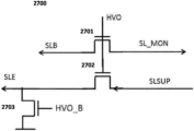
図27は、高電圧ソース線デコーダ回路2700を表す。高電圧ソース線デコーダ回路は、図示のように構成されたトランジスタ2701、2702及び2703を備える。トランジスタ2703は、ソース線を低電圧に選択解除するために使用される。トランジスタ2702は、高電圧をアレイのソース線に駆動するために使用され、トランジスタ2701はソース線の電圧を監視するために使用される。トランジスタ2702、2701及びドライバ回路(例えば、opa)は、PVT(プロセス、電圧、温度)及び変動電流負荷条件を維持するために、閉ループ方式(力/感知)で構成される。SLE(駆動ソース線ノード)及びSLB(監視されたソース線ノード)は、ソース線の一方の端部にあり得る。あるいは、SLEは、ソース線の一方の端部にあり、SLNが他方の端部にあり得る。
Figure 27 illustrates a high voltage source
図28は、図2に示されるタイプのメモリセルと共に使用するのに適切である、ワード線デコーダ回路2801、ソース線デコーダ回路2804及び高電圧レベルシフタ2808を備えるVMM高電圧デコード回路を示す。
Figure 28 shows a VMM high voltage decode circuit comprising a word
ワード線デコーダ回路2801は、図示のように構成された、PMOS選択トランジスタ2802(信号HVO_Bによって制御される)及びNMOS選択トランジスタ2803(信号HVO_Bによって制御される)を備える。
Word
ソース線デコーダ回路2804は、NMOS監視トランジスタ2805(信号HVOによって制御される)と、駆動トランジスタ2806(信号HVOによって制御される)と、図示のように構成された(信号HVO_Bによって制御される)トランジスタ2807を備える。
The source
高電圧レベルシフタ2808は、有効な信号ENを受信し、高電圧信号HV及びその補体HVO_Bを出力する。
The high
図29は、図3に示されるタイプのメモリセルと共に使用するのに適切である、消去ゲートデコーダ回路2901、制御ゲートデコーダ回路2904、ソース線デコーダ回路2907及び高電圧レベルシフタ2911を備えるVMM高電圧デコード回路を示す。
Figure 29 shows a VMM high voltage decode circuit comprising an erase
消去ゲートデコーダ回路2901及び制御ゲートデコーダ回路2904は、図28のワード線デコーダ回路2801と同じ設計を使用する。
The erase
ソース線デコーダ回路2907は、図28のソース線デコーダ回路2804と同じ設計を使用する。
Source
高電圧レベルシフタ2911は、図28の高電圧レベルシフタ2808と同じ設計を使用する。
High
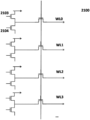
図30は、例示的なワード線WL0、WL1、WL2、及びWL3のワード線デコーダ300を示す。例示的なワード線WL0は、プルアップトランジスタ3001及びプルダウントランジスタ3002に結合される。プルアップトランジスタ3001が活性化されると、WL0が有効になる。プルダウントランジスタ3002が活性化されると、WL0は無効にされる。図30の関数は、絶縁トランジスタを有さない図21と同様である。
Figure 30 shows a word line decoder 300 for example word lines WL0, WL1, WL2, and WL3. Example word line WL0 is coupled to pull-up
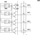
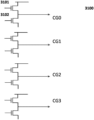
図31は、例示的な制御ゲート線CG0、CG1、CG2、及びCG3の制御ゲートデコーダ3100を示す。例示的な制御ゲート線CG0は、プルアップトランジスタ3101及びプルダウントランジスタ3102に結合される。プルアップトランジスタ3101が活性化されると、CG0が有効にされる。プルダウントランジスタ3102が活性化されると、CG0は無効にされる。図31の選択及び選択解除関数は、制御ゲートの図30の選択及び選択関数と同様である。
FIG. 31 shows a
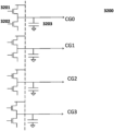
図32は、例示的な制御ゲート線CG0、CG1、CG2、及びCG3の制御ゲートデコーダ3200を示す。制御ゲートデコーダ3200は、制御ゲートデコーダ3200が各制御ゲート線に結合されたコンデンサ3203などのコンデンサを含むことを除いて、制御ゲートデコーダ3100と同様である。これらのサンプルアンドホールド(S/H)コンデンサは、動作前に各制御ゲート線にプリチャージバイアスを提供することができ、S/Hコンデンサの電圧が制御ゲート線の(浮遊)電圧源として機能することを意味する。S/Hコンデンサは、メモリセルからの制御ゲート容量によって提供され得る。
Figure 32 shows a
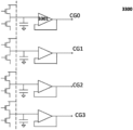
図33は、例示的な制御ゲート線CG0、CG1、CG2、及びCG3の制御ゲートデコーダ3300を示す。制御ゲートデコーダ3300は、制御ゲートデコーダ3300がバッファ3301(opaなど)を更に備えることを除いて、制御ゲートデコーダ3200と同様である。
FIG. 33 illustrates a
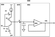
図34は、電流電圧回路3400を示す。回路は、構成されたダイオード接続基準セル回路3450及びサンプルアンドホールド回路3460を備える。回路3450は、入力電流源3401、NMOSトランジスタ3402、カスコーディングバイアストランジスタ3403、及び基準メモリセル3404を備える。サンプルアンドホールド回路は、スイッチ3405及びS/Hコンデンサ3406からなる。メモリ3404は、ワード線を供給するためなど、入力電流を電圧に変換するために、ビット線のバイアスを有するダイオード接続構成でバイアスされる。
Figure 34 shows a current-to-
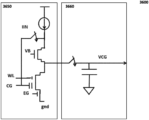
図35は、電流電圧回路3500を示しており、電流電圧回路3500は、電流電圧回路3400と同様であるが、それにS/Hコンデンサの後に増幅器3501を追加している。電流電圧回路3500は、構成されたダイオード接続基準セル回路3550、サンプルアンドホールド回路3470、及び増幅器ステージ3562を備える。
Figure 35 shows a current-
図36は、ダイオード接続構成における制御ゲートの電流電圧回路3400と同じ設計である電流電圧回路3600を示す。電流電圧回路3600は、構成されたダイオード接続基準セル回路3650及びサンプルアンドホールド回路3660を備える。
Figure 36 shows a current-
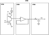
図37は、基準回路3750とS/H回路3760との間にバッファ3790が配置される電流電圧回路3700を示す。
Figure 37 shows a current-
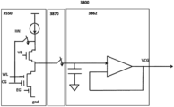
図38は、ダイオード接続構成で接続された制御ゲートを有する図35と同様の電流電圧回路3800を示す。電流電圧回路3800は、構成されたダイオード接続基準セル回路3550、サンプルアンドホールド回路3870、及び増幅器ステージ3862を備える。
FIG. 38 shows a current-
図39は、図2のメモリセルに適用された図34と同様の電流電圧回路3900を示す。電流電圧回路3900は、構成されたダイオード接続基準セル回路3950及びサンプルアンドホールド回路3960を備える。
FIG. 39 shows a current-
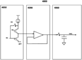
図40は、図2のメモリセルに適用される図37と同様の電流電圧回路4000を示し、バッファ4090は、基準回路4050とS/H回路4060との間に配置される。
Figure 40 shows a current-
図41は、図2のメモリセルに適用された図38と同様の電流電圧回路4100を示す。電流電圧回路4100は、構成されたダイオード接続基準セル回路4150、サンプルアンドホールド回路4170、及び増幅器ステージ4162を備える。
FIG. 41 shows a current-
本明細書で使用される場合、「の上方に(over)」及び「に(on)」という用語は両方とも、「に直接」(中間材料、要素、又は空間がそれらの間に何ら配設されない)、及び「の上に間接的に」(中間材料、要素、又は空間がそれらの間に配設される)を包括的に含むことに留意するべきである。同様に、「隣接した」という用語は、「直接隣接した」(中間材料、要素、又は空間がそれらの間に何ら配設されない)、及び「間接的に隣接した」(中間材料、要素、又は空間がそれらの間に配設される)を含み、「に取り付けられた」は、「に直接取り付けられた」(中間材料、要素、又は空間がそれらの間に何ら配設されない)、及び「に間接的に取り付けられた」(中間材料、要素、又は空間がそれらの間に配設される)を含み、「電気的に結合された」は、「に直接電気的に結合された」(要素を一緒に電気的に連結する中間材料又は要素がそれらの間にない)、及び「に間接的に電気的に結合された」(要素を一緒に電気的に連結する中間材料又は要素がそれらの間にある)を含む。例えば、要素を「基板の上方に」形成することは、その要素を基板に直接、中間材料/要素をそれらの間に何ら伴わずに、形成すること、及びその要素を基板の上に間接的に、1つ以上の中間材料/要素をそれらの間に伴って、形成することを含み得る。 It should be noted that, as used herein, both the terms "over" and "on" are inclusive of "directly" (without any intermediate material, element, or space disposed between them) and "indirectly on" (with intermediate material, element, or space disposed between them). Similarly, the term "adjacent" includes "directly adjacent" (without any intermediate material, element, or space disposed between them) and "indirectly adjacent" (with intermediate material, element, or space disposed between them), "attached" includes "directly attached" (without any intermediate material, element, or space disposed between them) and "indirectly attached to" (with intermediate material, element, or space disposed between them), and "electrically coupled" includes "directly electrically coupled" (without any intermediate material or element electrically coupling the elements together) and "indirectly electrically coupled to" (with intermediate material or element electrically coupling the elements together). For example, forming an element "above a substrate" can include forming the element directly on the substrate, without any intermediate materials/elements between them, and forming the element indirectly on the substrate, with one or more intermediate materials/elements between them.
Claims (2)
行及び列に編成された不揮発性メモリセルのアレイを備えるベクトルマトリクス乗算アレイであって、各不揮発性メモリセルは、ビット線端子、ワード線端子、及びソース線端子を含み、不揮発メモリセルの各行は、前記行内の前記不揮発メモリセルの前記ワード端子を介してワード線に接続され、かつ、前記行内の前記不揮発性メモリセルの前記ソース端子を線介してソース線に接続され、不揮発性メモリセルの各列は、前記列内の前記不揮発性メモリセルの前記ビット線端子を介してビット線に接続される、ベクトルマトリクス乗算アレイと、
前記不揮発性メモリセルの前記ワード線端子に結合されたワード線デコーダ回路であって、低電圧又は高電圧を結合されたワード線端子に印加することができる、ワード線デコーダ回路と、
前記不揮発性メモリセルの前記ソース線端子に結合されたソース線デコーダ回路であって、前記ソース線デコーダ回路は、各行に対して、前記行の前記ソース線を低電圧に選択的に結合する第1のトランジスタ、及び、前記行の前記ソース線を高電圧に選択的に結合する第2のトランジスタを備える、ソース線デコーダ回路と、を備える、システム。 1. An analog neuromorphic memory system, comprising:
a vector matrix multiplication array comprising an array of non-volatile memory cells organized into rows and columns, each non-volatile memory cell including a bit line terminal, a word line terminal, and a source line terminal, each row of non-volatile memory cells being connected to a word line via the word terminals of the non-volatile memory cells in the row and to a source line via lines of the source terminals of the non-volatile memory cells in the row, and each column of non-volatile memory cells being connected to a bit line via the bit line terminals of the non-volatile memory cells in the column ;
a word line decoder circuit coupled to the word line terminals of the non-volatile memory cells, the word line decoder circuit being capable of applying a low voltage or a high voltage to the coupled word line terminals;
a source line decoder circuit coupled to the source line terminals of the non-volatile memory cells , the source line decoder circuit comprising, for each row, a first transistor that selectively couples the source line of the row to a low voltage and a second transistor that selectively couples the source line of the row to a high voltage .
前記不揮発性メモリセルの前記消去ゲート端子に結合された消去ゲートデコーダ回路であって、低電圧又は高電圧を結合された消去ゲート端子に印加することができる、消去ゲートデコーダ回路を更に備える、請求項1に記載のシステム。
Each non-volatile memory cell further comprises an erase gate terminal , each row of non-volatile memory cells is connected to an erase gate line via the erase gate terminals of the non-volatile memory cells in the row, and the system further comprises:
10. The system of claim 1, further comprising an erase gate decoder circuit coupled to the erase gate terminal of the non-volatile memory cell, the erase gate decoder circuit being capable of applying a low voltage or a high voltage to the coupled erase gate terminal .
Priority Applications (1)
| Application Number | Priority Date | Filing Date | Title |
|---|---|---|---|
| JP2024146132A JP7791950B2 (en) | 2018-03-14 | 2024-08-28 | Decoders for Analog Neural Memories in Deep Learning Artificial Neural Networks |
Applications Claiming Priority (5)
| Application Number | Priority Date | Filing Date | Title |
|---|---|---|---|
| US201862642884P | 2018-03-14 | 2018-03-14 | |
| US62/642,884 | 2018-03-14 | ||
| US15/991,890 US11087207B2 (en) | 2018-03-14 | 2018-05-29 | Decoders for analog neural memory in deep learning artificial neural network |
| US15/991,890 | 2018-05-29 | ||
| JP2020548740A JP7253563B2 (en) | 2018-03-14 | 2019-01-24 | Decoder for Analog Neural Memory in Deep Learning Artificial Neural Networks |
Related Parent Applications (1)
| Application Number | Title | Priority Date | Filing Date |
|---|---|---|---|
| JP2020548740A Division JP7253563B2 (en) | 2018-03-14 | 2019-01-24 | Decoder for Analog Neural Memory in Deep Learning Artificial Neural Networks |
Related Child Applications (1)
| Application Number | Title | Priority Date | Filing Date |
|---|---|---|---|
| JP2024146132A Division JP7791950B2 (en) | 2018-03-14 | 2024-08-28 | Decoders for Analog Neural Memories in Deep Learning Artificial Neural Networks |
Publications (2)
| Publication Number | Publication Date |
|---|---|
| JP2023093463A JP2023093463A (en) | 2023-07-04 |
| JP7547536B2 true JP7547536B2 (en) | 2024-09-09 |
Family
ID=67905831
Family Applications (3)
| Application Number | Title | Priority Date | Filing Date |
|---|---|---|---|
| JP2020548740A Active JP7253563B2 (en) | 2018-03-14 | 2019-01-24 | Decoder for Analog Neural Memory in Deep Learning Artificial Neural Networks |
| JP2023049721A Active JP7547536B2 (en) | 2018-03-14 | 2023-03-27 | Decoders for Analog Neural Memories in Deep Learning Artificial Neural Networks |
| JP2024146132A Active JP7791950B2 (en) | 2018-03-14 | 2024-08-28 | Decoders for Analog Neural Memories in Deep Learning Artificial Neural Networks |
Family Applications Before (1)
| Application Number | Title | Priority Date | Filing Date |
|---|---|---|---|
| JP2020548740A Active JP7253563B2 (en) | 2018-03-14 | 2019-01-24 | Decoder for Analog Neural Memory in Deep Learning Artificial Neural Networks |
Family Applications After (1)
| Application Number | Title | Priority Date | Filing Date |
|---|---|---|---|
| JP2024146132A Active JP7791950B2 (en) | 2018-03-14 | 2024-08-28 | Decoders for Analog Neural Memories in Deep Learning Artificial Neural Networks |
Country Status (7)
| Country | Link |
|---|---|
| US (4) | US11087207B2 (en) |
| EP (4) | EP4650990A2 (en) |
| JP (3) | JP7253563B2 (en) |
| KR (4) | KR20250035044A (en) |
| CN (2) | CN119599075A (en) |
| TW (2) | TWI764503B (en) |
| WO (1) | WO2019177698A1 (en) |
Families Citing this family (28)
| Publication number | Priority date | Publication date | Assignee | Title |
|---|---|---|---|---|
| US10891080B1 (en) * | 2018-06-04 | 2021-01-12 | Mentium Technologies Inc. | Management of non-volatile memory arrays |
| US11500442B2 (en) * | 2019-01-18 | 2022-11-15 | Silicon Storage Technology, Inc. | System for converting neuron current into neuron current-based time pulses in an analog neural memory in a deep learning artificial neural network |
| US11893478B2 (en) | 2019-01-18 | 2024-02-06 | Silicon Storage Technology, Inc. | Programmable output blocks for analog neural memory in a deep learning artificial neural network |
| US11270763B2 (en) | 2019-01-18 | 2022-03-08 | Silicon Storage Technology, Inc. | Neural network classifier using array of three-gate non-volatile memory cells |
| US11023559B2 (en) | 2019-01-25 | 2021-06-01 | Microsemi Soc Corp. | Apparatus and method for combining analog neural net with FPGA routing in a monolithic integrated circuit |
| US11423979B2 (en) | 2019-04-29 | 2022-08-23 | Silicon Storage Technology, Inc. | Decoding system and physical layout for analog neural memory in deep learning artificial neural network |
| CN111313914B (en) * | 2019-11-05 | 2021-09-28 | 北京航空航天大学 | SCL simplified decoding method based on neural network classifier |
| US12124942B2 (en) * | 2019-12-03 | 2024-10-22 | Anaflash Inc. | Serialized neural network computing unit |
| TWI789589B (en) * | 2020-02-04 | 2023-01-11 | 旺宏電子股份有限公司 | Spiking neural networks circuit and operation method thereof |
| US11600321B2 (en) * | 2020-03-05 | 2023-03-07 | Silicon Storage Technology, Inc. | Analog neural memory array storing synapsis weights in differential cell pairs in artificial neural network |
| KR102899213B1 (en) | 2020-03-25 | 2025-12-10 | 삼성전자주식회사 | Neuromorphic device and method of using the same |
| US11289164B2 (en) * | 2020-06-03 | 2022-03-29 | Silicon Storage Technology, Inc. | Word line and control gate line tandem decoder for analog neural memory in deep learning artificial neural network |
| US11875852B2 (en) * | 2020-07-06 | 2024-01-16 | Silicon Storage Technology, Inc. | Adaptive bias decoder to provide a voltage to a control gate line in an analog neural memory array in artificial neural network |
| CN113946278B (en) * | 2020-07-16 | 2025-01-21 | 慧荣科技股份有限公司 | Data reading method and device for host performance acceleration mode |
| FR3113326B1 (en) * | 2020-08-06 | 2023-01-06 | St Microelectronics Rousset | Intra-memory convolutional calculation method and corresponding integrated circuit |
| CN112633487B (en) * | 2020-12-25 | 2022-05-20 | 北京大学 | Maximum pooling layer circuit of convolutional neural network |
| CN112784971A (en) * | 2021-01-13 | 2021-05-11 | 天津智模科技有限公司 | Neural network operation circuit based on digital-analog hybrid neurons |
| US12033699B2 (en) * | 2021-02-02 | 2024-07-09 | Macronix International Co., Ltd. | Memory device and operation method thereof for performing multiply accumulate operation |
| TWI821746B (en) * | 2021-02-02 | 2023-11-11 | 旺宏電子股份有限公司 | Memory device and operation method thereof |
| EP4668165A2 (en) * | 2021-05-18 | 2025-12-24 | Silicon Storage Technology, Inc. | Split array architecture for analog neural memory in a deep learning artificial neural network |
| US11996137B2 (en) * | 2021-05-21 | 2024-05-28 | Taiwan Semiconductor Manufacturing Company, Ltd. | Compute in memory (CIM) memory array |
| US20230048411A1 (en) * | 2021-08-02 | 2023-02-16 | Silicon Storage Technology, Inc. | Input circuitry for analog neural memory in a deep learning artificial neural network |
| US11935603B2 (en) * | 2021-11-04 | 2024-03-19 | Infineon Technologies LLC | Erase power loss indicator (EPLI) implementation in flash memory device |
| US12499943B2 (en) | 2022-01-06 | 2025-12-16 | Samsung Electronics Co., Ltd. | Spiking neural network device, nonvolatile memory device, and operation method thereof |
| KR20230166777A (en) | 2022-05-31 | 2023-12-07 | 삼성전자주식회사 | Neuromorphic device |
| CN115688897B (en) * | 2023-01-03 | 2023-03-31 | 浙江大学杭州国际科创中心 | Low-power-consumption compact Relu activation function neuron circuit |
| KR102885729B1 (en) * | 2023-03-31 | 2025-11-13 | 서울대학교산학협력단 | Update cell, neuromorphic circuit including the same, and method of operating neuromorphic circuit |
| CN120981817A (en) * | 2023-03-31 | 2025-11-18 | 首尔大学校产学协力团 | The updating unit, including its neuromorphic circuitry, and the operation method of the neuromorphic circuitry. |
Citations (2)
| Publication number | Priority date | Publication date | Assignee | Title |
|---|---|---|---|---|
| WO2017200883A1 (en) | 2016-05-17 | 2017-11-23 | Silicon Storage Technology, Inc. | Deep learning neural network classifier using non-volatile memory array |
| WO2017200888A1 (en) | 2016-05-18 | 2017-11-23 | Silicon Storage Technology, Inc. | Improved flash memory cell associated decoders |
Family Cites Families (85)
| Publication number | Priority date | Publication date | Assignee | Title |
|---|---|---|---|---|
| FR2603414B1 (en) | 1986-08-29 | 1988-10-28 | Bull Sa | READING AMPLIFIER |
| JP3122756B2 (en) | 1991-01-12 | 2001-01-09 | 直 柴田 | Semiconductor device |
| US5621336A (en) | 1989-06-02 | 1997-04-15 | Shibata; Tadashi | Neuron circuit |
| JPH0318985A (en) | 1989-06-16 | 1991-01-28 | Hitachi Ltd | information processing equipment |
| US4961002A (en) | 1989-07-13 | 1990-10-02 | Intel Corporation | Synapse cell employing dual gate transistor structure |
| GB2236881B (en) * | 1989-10-11 | 1994-01-12 | Intel Corp | Improved synapse cell employing dual gate transistor structure |
| KR920010344B1 (en) | 1989-12-29 | 1992-11-27 | 삼성전자주식회사 | Configuration Method of Semiconductor Memory Array |
| US5029130A (en) | 1990-01-22 | 1991-07-02 | Silicon Storage Technology, Inc. | Single transistor non-valatile electrically alterable semiconductor memory device |
| US5146602A (en) | 1990-12-26 | 1992-09-08 | Intel Corporation | Method of increasing the accuracy of an analog neural network and the like |
| US5138576A (en) | 1991-11-06 | 1992-08-11 | Altera Corporation | Method and apparatus for erasing an array of electrically erasable EPROM cells |
| DE69319162T2 (en) | 1992-03-26 | 1999-03-25 | Hitachi Vlsi Engineering Corp., Kodaira, Tokio/Tokyo | Flash memory |
| US5336936A (en) | 1992-05-06 | 1994-08-09 | Synaptics, Incorporated | One-transistor adaptable analog storage element and array |
| US5264734A (en) | 1992-05-19 | 1993-11-23 | Intel Corporation | Difference calculating neural network utilizing switched capacitors |
| US5256911A (en) | 1992-06-10 | 1993-10-26 | Intel Corporation | Neural network with multiplexed snyaptic processing |
| JPH0628875A (en) * | 1992-07-10 | 1994-02-04 | Sony Corp | Erasing method of flash type E2 PROM |
| US5386132A (en) | 1992-11-02 | 1995-01-31 | Wong; Chun C. D. | Multimedia storage system with highly compact memory device |
| JP2835272B2 (en) | 1993-12-21 | 1998-12-14 | 株式会社東芝 | Semiconductor storage device |
| KR0151623B1 (en) | 1994-12-07 | 1998-10-01 | 문정환 | Ipyrom cell and preparation method thereof |
| US5825063A (en) | 1995-03-07 | 1998-10-20 | California Institute Of Technology | Three-terminal silicon synaptic device |
| US5554874A (en) | 1995-06-05 | 1996-09-10 | Quantum Effect Design, Inc. | Six-transistor cell with wide bit-line pitch, double words lines, and bit-line contact shared among four cells |
| US5721702A (en) | 1995-08-01 | 1998-02-24 | Micron Quantum Devices, Inc. | Reference voltage generator using flash memory cells |
| US6683645B1 (en) | 1995-12-01 | 2004-01-27 | Qinetiq Limited | Imaging system with low sensitivity to variation in scene illumination |
| JPH10320989A (en) * | 1997-05-16 | 1998-12-04 | Toshiba Microelectron Corp | Non-volatile semiconductor memory |
| TW332954B (en) * | 1997-05-16 | 1998-06-01 | Ind Tech Res Inst | Data processing method and apparatus in neural network system |
| US6222777B1 (en) | 1999-04-09 | 2001-04-24 | Sun Microsystems, Inc. | Output circuit for alternating multiple bit line per column memory architecture |
| KR100338772B1 (en) | 2000-03-10 | 2002-05-31 | 윤종용 | Word line driver having divided bias line in non-volatile memory device and method thereof |
| US6829598B2 (en) | 2000-10-02 | 2004-12-07 | Texas Instruments Incorporated | Method and apparatus for modeling a neural synapse function by utilizing a single conventional MOSFET |
| US6563167B2 (en) | 2001-01-05 | 2003-05-13 | Silicon Storage Technology, Inc. | Semiconductor memory array of floating gate memory cells with floating gates having multiple sharp edges |
| US6563733B2 (en) | 2001-05-24 | 2003-05-13 | Winbond Electronics Corporation | Memory array architectures based on a triple-polysilicon source-side injection non-volatile memory cell |
| US6912152B2 (en) * | 2002-02-22 | 2005-06-28 | Kabushiki Kaisha Toshiba | Magnetic random access memory |
| JP2005522071A (en) | 2002-03-22 | 2005-07-21 | ジョージア テック リサーチ コーポレイション | Floating gate analog circuit |
| JP4273718B2 (en) | 2002-08-16 | 2009-06-03 | ソニー株式会社 | Current sampling circuit and current output type driving circuit using the same |
| US6747310B2 (en) | 2002-10-07 | 2004-06-08 | Actrans System Inc. | Flash memory cells with separated self-aligned select and erase gates, and process of fabrication |
| ITMI20022240A1 (en) * | 2002-10-22 | 2004-04-23 | Atmel Corp | FLASH MEMORY ARCHITECTURE WITH MODE CANCELLATION |
| JP2004171686A (en) | 2002-11-20 | 2004-06-17 | Renesas Technology Corp | Nonvolatile semiconductor memory device, and data erasing method therefor |
| US6822910B2 (en) | 2002-12-29 | 2004-11-23 | Macronix International Co., Ltd. | Non-volatile memory and operating method thereof |
| US6856551B2 (en) | 2003-02-06 | 2005-02-15 | Sandisk Corporation | System and method for programming cells in non-volatile integrated memory devices |
| TWI220560B (en) | 2003-10-27 | 2004-08-21 | Powerchip Semiconductor Corp | NAND flash memory cell architecture, NAND flash memory cell array, manufacturing method and operating method of the same |
| JP4585213B2 (en) * | 2004-03-24 | 2010-11-24 | 株式会社日立製作所 | Data protection method, authentication method, and program |
| JP4157065B2 (en) * | 2004-03-29 | 2008-09-24 | 株式会社東芝 | Semiconductor memory device |
| US7315056B2 (en) | 2004-06-07 | 2008-01-01 | Silicon Storage Technology, Inc. | Semiconductor memory array of floating gate memory cells with program/erase and select gates |
| KR100632946B1 (en) | 2004-07-13 | 2006-10-12 | 삼성전자주식회사 | Nonvolatile Memory Device And Its Program Method |
| US7092290B2 (en) | 2004-11-16 | 2006-08-15 | Sandisk Corporation | High speed programming system with reduced over programming |
| TWI270199B (en) | 2005-01-31 | 2007-01-01 | Powerchip Semiconductor Corp | Non-volatile memory and manufacturing method and operating method thereof |
| US7304890B2 (en) | 2005-12-13 | 2007-12-04 | Atmel Corporation | Double byte select high voltage line for EEPROM memory block |
| US7626868B1 (en) | 2007-05-04 | 2009-12-01 | Flashsilicon, Incorporation | Level verification and adjustment for multi-level cell (MLC) non-volatile memory (NVM) |
| US7630246B2 (en) | 2007-06-18 | 2009-12-08 | Micron Technology, Inc. | Programming rate identification and control in a solid state memory |
| JP5045294B2 (en) | 2007-07-30 | 2012-10-10 | 富士通セミコンダクター株式会社 | Internal power supply circuit having cascode current mirror circuit |
| US20090039410A1 (en) | 2007-08-06 | 2009-02-12 | Xian Liu | Split Gate Non-Volatile Flash Memory Cell Having A Floating Gate, Control Gate, Select Gate And An Erase Gate With An Overhang Over The Floating Gate, Array And Method Of Manufacturing |
| US7800159B2 (en) * | 2007-10-24 | 2010-09-21 | Silicon Storage Technology, Inc. | Array of contactless non-volatile memory cells |
| US7894267B2 (en) | 2007-10-30 | 2011-02-22 | Spansion Llc | Deterministic programming algorithm that provides tighter cell distributions with a reduced number of programming pulses |
| US8464123B2 (en) * | 2009-05-07 | 2013-06-11 | Ramot At Tel Aviv University Ltd. | Matrix structure for block encoding |
| JP2010267341A (en) | 2009-05-15 | 2010-11-25 | Renesas Electronics Corp | Semiconductor device |
| US8553466B2 (en) * | 2010-03-04 | 2013-10-08 | Samsung Electronics Co., Ltd. | Non-volatile memory device, erasing method thereof, and memory system including the same |
| US8325521B2 (en) | 2010-10-08 | 2012-12-04 | Taiwan Semiconductor Manufacturing Company, Ltd. | Structure and inhibited operation of flash memory with split gate |
| US8892487B2 (en) | 2010-12-30 | 2014-11-18 | International Business Machines Corporation | Electronic synapses for reinforcement learning |
| JP2013041654A (en) | 2011-08-19 | 2013-02-28 | Toshiba Corp | Nonvolatile storage device |
| US8909576B2 (en) | 2011-09-16 | 2014-12-09 | International Business Machines Corporation | Neuromorphic event-driven neural computing architecture in a scalable neural network |
| US8760955B2 (en) | 2011-10-21 | 2014-06-24 | Taiwan Semiconductor Manufacturing Company, Ltd. | Electrical fuse memory arrays |
| JP3174679U (en) | 2012-01-20 | 2012-03-29 | 株式会社エラン | Firearm and blowback model gun |
| US9466732B2 (en) | 2012-08-23 | 2016-10-11 | Silicon Storage Technology, Inc. | Split-gate memory cell with depletion-mode floating gate channel, and method of making same |
| US9275748B2 (en) | 2013-03-14 | 2016-03-01 | Silicon Storage Technology, Inc. | Low leakage, low threshold voltage, split-gate flash cell operation |
| US10095718B2 (en) | 2013-10-16 | 2018-10-09 | University Of Tennessee Research Foundation | Method and apparatus for constructing a dynamic adaptive neural network array (DANNA) |
| US20150213898A1 (en) | 2014-01-27 | 2015-07-30 | Silicon Storage Technololgy, Inc. | Byte Erasable Non-volatile Memory Architecture And Method Of Erasing Same |
| US9431111B2 (en) * | 2014-07-08 | 2016-08-30 | Ememory Technology Inc. | One time programming memory cell, array structure and operating method thereof |
| US9286982B2 (en) | 2014-08-08 | 2016-03-15 | Silicon Storage Technology, Inc. | Flash memory system with EEPROM functionality |
| US9984754B2 (en) | 2014-09-29 | 2018-05-29 | Toshiba Memory Corporation | Memory device and method for operating the same |
| US10312248B2 (en) | 2014-11-12 | 2019-06-04 | Silicon Storage Technology, Inc. | Virtual ground non-volatile memory array |
| US9361991B1 (en) | 2014-12-23 | 2016-06-07 | Sandisk Technologies Inc. | Efficient scanning of nonvolatile memory blocks |
| CN105990367B (en) | 2015-02-27 | 2019-03-12 | 硅存储技术公司 | Nonvolatile memory cell array with ROM cells |
| US9595332B2 (en) * | 2015-06-15 | 2017-03-14 | Cypress Semiconductor Corporation | High speed, high voltage tolerant circuits in flash path |
| KR102473665B1 (en) * | 2015-07-28 | 2022-12-02 | 삼성전자주식회사 | Storage device and storage virtualization system |
| US10014318B2 (en) * | 2015-10-24 | 2018-07-03 | Monocithic 3D Inc | Semiconductor memory device, structure and methods |
| US10418369B2 (en) * | 2015-10-24 | 2019-09-17 | Monolithic 3D Inc. | Multi-level semiconductor memory device and structure |
| US10269440B2 (en) | 2016-05-17 | 2019-04-23 | Silicon Storage Technology, Inc. | Flash memory array with individual memory cell read, program and erase |
| KR102384654B1 (en) | 2016-05-17 | 2022-04-11 | 실리콘 스토리지 테크놀로지 인크 | Array of three-gate flash memory cells with individual memory cell read, program and erase |
| US9910827B2 (en) | 2016-07-01 | 2018-03-06 | Hewlett Packard Enterprise Development Lp | Vector-matrix multiplications involving negative values |
| US10748059B2 (en) | 2017-04-05 | 2020-08-18 | International Business Machines Corporation | Architecture for an electrochemical artificial neural network |
| US10134472B1 (en) * | 2017-06-30 | 2018-11-20 | International Business Machines Corporation | Floating gate architecture for deep neural network application |
| US10460817B2 (en) * | 2017-07-13 | 2019-10-29 | Qualcomm Incorporated | Multiple (multi-) level cell (MLC) non-volatile (NV) memory (NVM) matrix circuits for performing matrix computations with multi-bit input vectors |
| CN109522753B (en) | 2017-09-18 | 2020-11-06 | 清华大学 | Circuit structure and driving method thereof, chip and authentication method thereof, and electronic device |
| US10803943B2 (en) | 2017-11-29 | 2020-10-13 | Silicon Storage Technology, Inc. | Neural network classifier using array of four-gate non-volatile memory cells |
| US11354562B2 (en) * | 2018-01-03 | 2022-06-07 | Silicon Storage Technology, Inc. | Programmable neuron for analog non-volatile memory in deep learning artificial neural network |
| US10970441B1 (en) * | 2018-02-26 | 2021-04-06 | Washington University | System and method using neural networks for analog-to-information processors |
| US11270763B2 (en) | 2019-01-18 | 2022-03-08 | Silicon Storage Technology, Inc. | Neural network classifier using array of three-gate non-volatile memory cells |
-
2018
- 2018-05-29 US US15/991,890 patent/US11087207B2/en active Active
-
2019
- 2019-01-24 KR KR1020257007057A patent/KR20250035044A/en active Pending
- 2019-01-24 KR KR1020207022363A patent/KR102516399B1/en active Active
- 2019-01-24 KR KR1020237010513A patent/KR102604405B1/en active Active
- 2019-01-24 EP EP25206286.4A patent/EP4650990A2/en active Pending
- 2019-01-24 CN CN202411640536.XA patent/CN119599075A/en active Pending
- 2019-01-24 EP EP23212305.9A patent/EP4303772B1/en active Active
- 2019-01-24 EP EP19766740.5A patent/EP3766178B1/en active Active
- 2019-01-24 KR KR1020237039451A patent/KR102778708B1/en active Active
- 2019-01-24 JP JP2020548740A patent/JP7253563B2/en active Active
- 2019-01-24 WO PCT/US2019/015022 patent/WO2019177698A1/en not_active Ceased
- 2019-01-24 CN CN201980018434.5A patent/CN111886804B/en active Active
- 2019-01-24 EP EP25206284.9A patent/EP4650989A2/en active Pending
- 2019-03-11 TW TW110100981A patent/TWI764503B/en active
- 2019-03-11 TW TW108108059A patent/TWI717703B/en active
-
2021
- 2021-07-06 US US17/367,633 patent/US12099921B2/en active Active
-
2023
- 2023-03-27 JP JP2023049721A patent/JP7547536B2/en active Active
- 2023-11-27 US US18/520,277 patent/US20240095508A1/en active Pending
- 2023-11-27 US US18/520,500 patent/US12248870B2/en active Active
-
2024
- 2024-08-28 JP JP2024146132A patent/JP7791950B2/en active Active
Patent Citations (4)
| Publication number | Priority date | Publication date | Assignee | Title |
|---|---|---|---|---|
| WO2017200883A1 (en) | 2016-05-17 | 2017-11-23 | Silicon Storage Technology, Inc. | Deep learning neural network classifier using non-volatile memory array |
| JP2019517138A (en) | 2016-05-17 | 2019-06-20 | シリコン ストーリッジ テクノロージー インコーポレイテッドSilicon Storage Technology, Inc. | Deep Learning Neural Network Classifier Using Nonvolatile Memory Array |
| WO2017200888A1 (en) | 2016-05-18 | 2017-11-23 | Silicon Storage Technology, Inc. | Improved flash memory cell associated decoders |
| JP2019519059A (en) | 2016-05-18 | 2019-07-04 | シリコン ストーリッジ テクノロージー インコーポレイテッドSilicon Storage Technology, Inc. | Improved flash memory cell and associated decoder |
Also Published As
Similar Documents
| Publication | Publication Date | Title |
|---|---|---|
| JP7547536B2 (en) | Decoders for Analog Neural Memories in Deep Learning Artificial Neural Networks | |
| JP7668307B2 (en) | Decoding System and Physical Layout for Analog Neural Memory in Deep Learning Artificial Neural Networks | |
| JP7209811B2 (en) | A Configurable Analog Neural Memory System for Deep Learning Neural Networks | |
| JP7620059B2 (en) | Word Line and Control Gate Line Tandem Decoder for Analog Neural Memory in Deep Learning Artificial Neural Networks | |
| KR102912832B1 (en) | Decoding system and physical layout for analog neural memory in deep learning artificial neural network | |
| KR20260017002A (en) | Decoding system and physical layout for analog neural memory in deep learning artificial neural network |
Legal Events
| Date | Code | Title | Description |
|---|---|---|---|
| A521 | Request for written amendment filed |
Free format text: JAPANESE INTERMEDIATE CODE: A523 Effective date: 20230424 |
|
| A621 | Written request for application examination |
Free format text: JAPANESE INTERMEDIATE CODE: A621 Effective date: 20230424 |
|
| A131 | Notification of reasons for refusal |
Free format text: JAPANESE INTERMEDIATE CODE: A131 Effective date: 20240416 |
|
| A521 | Request for written amendment filed |
Free format text: JAPANESE INTERMEDIATE CODE: A523 Effective date: 20240716 |
|
| TRDD | Decision of grant or rejection written | ||
| A01 | Written decision to grant a patent or to grant a registration (utility model) |
Free format text: JAPANESE INTERMEDIATE CODE: A01 Effective date: 20240730 |
|
| A61 | First payment of annual fees (during grant procedure) |
Free format text: JAPANESE INTERMEDIATE CODE: A61 Effective date: 20240828 |
|
| R150 | Certificate of patent or registration of utility model |
Ref document number: 7547536 Country of ref document: JP Free format text: JAPANESE INTERMEDIATE CODE: R150 |