JP7512349B2 - 回折格子の製造 - Google Patents
回折格子の製造 Download PDFInfo
- Publication number
- JP7512349B2 JP7512349B2 JP2022178867A JP2022178867A JP7512349B2 JP 7512349 B2 JP7512349 B2 JP 7512349B2 JP 2022178867 A JP2022178867 A JP 2022178867A JP 2022178867 A JP2022178867 A JP 2022178867A JP 7512349 B2 JP7512349 B2 JP 7512349B2
- Authority
- JP
- Japan
- Prior art keywords
- substrate
- angled
- hard mask
- mesas
- forming
- Prior art date
- Legal status (The legal status is an assumption and is not a legal conclusion. Google has not performed a legal analysis and makes no representation as to the accuracy of the status listed.)
- Active
Links
Images


Classifications
-
- G—PHYSICS
- G02—OPTICS
- G02B—OPTICAL ELEMENTS, SYSTEMS OR APPARATUS
- G02B5/00—Optical elements other than lenses
- G02B5/18—Diffraction gratings
-
- G—PHYSICS
- G02—OPTICS
- G02B—OPTICAL ELEMENTS, SYSTEMS OR APPARATUS
- G02B27/00—Optical systems or apparatus not provided for by any of the groups G02B1/00 - G02B26/00, G02B30/00
- G02B27/09—Beam shaping, e.g. changing the cross-sectional area, not otherwise provided for
- G02B27/0938—Using specific optical elements
- G02B27/0944—Diffractive optical elements, e.g. gratings, holograms
-
- G—PHYSICS
- G02—OPTICS
- G02B—OPTICAL ELEMENTS, SYSTEMS OR APPARATUS
- G02B5/00—Optical elements other than lenses
- G02B5/18—Diffraction gratings
- G02B5/1847—Manufacturing methods
- G02B5/1857—Manufacturing methods using exposure or etching means, e.g. holography, photolithography, exposure to electron or ion beams
-
- G—PHYSICS
- G02—OPTICS
- G02B—OPTICAL ELEMENTS, SYSTEMS OR APPARATUS
- G02B6/00—Light guides; Structural details of arrangements comprising light guides and other optical elements, e.g. couplings
- G02B6/10—Light guides; Structural details of arrangements comprising light guides and other optical elements, e.g. couplings of the optical waveguide type
- G02B6/12—Light guides; Structural details of arrangements comprising light guides and other optical elements, e.g. couplings of the optical waveguide type of the integrated circuit kind
- G02B6/122—Basic optical elements, e.g. light-guiding paths
- G02B6/124—Geodesic lenses or integrated gratings
-
- G—PHYSICS
- G02—OPTICS
- G02B—OPTICAL ELEMENTS, SYSTEMS OR APPARATUS
- G02B6/00—Light guides; Structural details of arrangements comprising light guides and other optical elements, e.g. couplings
- G02B6/10—Light guides; Structural details of arrangements comprising light guides and other optical elements, e.g. couplings of the optical waveguide type
- G02B6/12—Light guides; Structural details of arrangements comprising light guides and other optical elements, e.g. couplings of the optical waveguide type of the integrated circuit kind
- G02B6/13—Integrated optical circuits characterised by the manufacturing method
- G02B6/136—Integrated optical circuits characterised by the manufacturing method by etching
-
- G—PHYSICS
- G03—PHOTOGRAPHY; CINEMATOGRAPHY; ANALOGOUS TECHNIQUES USING WAVES OTHER THAN OPTICAL WAVES; ELECTROGRAPHY; HOLOGRAPHY
- G03F—PHOTOMECHANICAL PRODUCTION OF TEXTURED OR PATTERNED SURFACES, e.g. FOR PRINTING, FOR PROCESSING OF SEMICONDUCTOR DEVICES; MATERIALS THEREFOR; ORIGINALS THEREFOR; APPARATUS SPECIALLY ADAPTED THEREFOR
- G03F1/00—Originals for photomechanical production of textured or patterned surfaces, e.g., masks, photo-masks, reticles; Mask blanks or pellicles therefor; Containers specially adapted therefor; Preparation thereof
- G03F1/68—Preparation processes not covered by groups G03F1/20 - G03F1/50
- G03F1/80—Etching
-
- G—PHYSICS
- G03—PHOTOGRAPHY; CINEMATOGRAPHY; ANALOGOUS TECHNIQUES USING WAVES OTHER THAN OPTICAL WAVES; ELECTROGRAPHY; HOLOGRAPHY
- G03F—PHOTOMECHANICAL PRODUCTION OF TEXTURED OR PATTERNED SURFACES, e.g. FOR PRINTING, FOR PROCESSING OF SEMICONDUCTOR DEVICES; MATERIALS THEREFOR; ORIGINALS THEREFOR; APPARATUS SPECIALLY ADAPTED THEREFOR
- G03F7/00—Photomechanical, e.g. photolithographic, production of textured or patterned surfaces, e.g. printing surfaces; Materials therefor, e.g. comprising photoresists; Apparatus specially adapted therefor
- G03F7/0002—Lithographic processes using patterning methods other than those involving the exposure to radiation, e.g. by stamping
-
- G—PHYSICS
- G03—PHOTOGRAPHY; CINEMATOGRAPHY; ANALOGOUS TECHNIQUES USING WAVES OTHER THAN OPTICAL WAVES; ELECTROGRAPHY; HOLOGRAPHY
- G03F—PHOTOMECHANICAL PRODUCTION OF TEXTURED OR PATTERNED SURFACES, e.g. FOR PRINTING, FOR PROCESSING OF SEMICONDUCTOR DEVICES; MATERIALS THEREFOR; ORIGINALS THEREFOR; APPARATUS SPECIALLY ADAPTED THEREFOR
- G03F7/00—Photomechanical, e.g. photolithographic, production of textured or patterned surfaces, e.g. printing surfaces; Materials therefor, e.g. comprising photoresists; Apparatus specially adapted therefor
- G03F7/20—Exposure; Apparatus therefor
- G03F7/2022—Multi-step exposure, e.g. hybrid; backside exposure; blanket exposure, e.g. for image reversal; edge exposure, e.g. for edge bead removal; corrective exposure
-
- H—ELECTRICITY
- H10—SEMICONDUCTOR DEVICES; ELECTRIC SOLID-STATE DEVICES NOT OTHERWISE PROVIDED FOR
- H10P—GENERIC PROCESSES OR APPARATUS FOR THE MANUFACTURE OR TREATMENT OF DEVICES COVERED BY CLASS H10
- H10P14/00—Formation of materials, e.g. in the shape of layers or pillars
- H10P14/60—Formation of materials, e.g. in the shape of layers or pillars of insulating materials
- H10P14/63—Formation of materials, e.g. in the shape of layers or pillars of insulating materials characterised by the formation processes
- H10P14/6326—Deposition processes
- H10P14/6328—Deposition from the gas or vapour phase
- H10P14/6329—Deposition from the gas or vapour phase using physical ablation of a target, e.g. physical vapour deposition or pulsed laser deposition
-
- H—ELECTRICITY
- H10—SEMICONDUCTOR DEVICES; ELECTRIC SOLID-STATE DEVICES NOT OTHERWISE PROVIDED FOR
- H10P—GENERIC PROCESSES OR APPARATUS FOR THE MANUFACTURE OR TREATMENT OF DEVICES COVERED BY CLASS H10
- H10P14/00—Formation of materials, e.g. in the shape of layers or pillars
- H10P14/60—Formation of materials, e.g. in the shape of layers or pillars of insulating materials
- H10P14/63—Formation of materials, e.g. in the shape of layers or pillars of insulating materials characterised by the formation processes
- H10P14/6326—Deposition processes
- H10P14/6328—Deposition from the gas or vapour phase
- H10P14/6334—Deposition from the gas or vapour phase using decomposition or reaction of gaseous or vapour phase compounds, i.e. chemical vapour deposition
- H10P14/6339—Deposition from the gas or vapour phase using decomposition or reaction of gaseous or vapour phase compounds, i.e. chemical vapour deposition deposition by cyclic CVD, e.g. ALD, ALE or pulsed CVD
-
- H—ELECTRICITY
- H10—SEMICONDUCTOR DEVICES; ELECTRIC SOLID-STATE DEVICES NOT OTHERWISE PROVIDED FOR
- H10P—GENERIC PROCESSES OR APPARATUS FOR THE MANUFACTURE OR TREATMENT OF DEVICES COVERED BY CLASS H10
- H10P50/00—Etching of wafers, substrates or parts of devices
-
- H—ELECTRICITY
- H10—SEMICONDUCTOR DEVICES; ELECTRIC SOLID-STATE DEVICES NOT OTHERWISE PROVIDED FOR
- H10P—GENERIC PROCESSES OR APPARATUS FOR THE MANUFACTURE OR TREATMENT OF DEVICES COVERED BY CLASS H10
- H10P76/00—Manufacture or treatment of masks on semiconductor bodies, e.g. by lithography or photolithography
- H10P76/40—Manufacture or treatment of masks on semiconductor bodies, e.g. by lithography or photolithography of masks comprising inorganic materials
- H10P76/408—Manufacture or treatment of masks on semiconductor bodies, e.g. by lithography or photolithography of masks comprising inorganic materials characterised by their sizes, orientations, dispositions, behaviours or shapes
- H10P76/4085—Manufacture or treatment of masks on semiconductor bodies, e.g. by lithography or photolithography of masks comprising inorganic materials characterised by their sizes, orientations, dispositions, behaviours or shapes characterised by the processes involved to create the masks
Landscapes
- Physics & Mathematics (AREA)
- General Physics & Mathematics (AREA)
- Optics & Photonics (AREA)
- Engineering & Computer Science (AREA)
- Microelectronics & Electronic Packaging (AREA)
- Manufacturing & Machinery (AREA)
- Diffracting Gratings Or Hologram Optical Elements (AREA)
- Optical Integrated Circuits (AREA)
- Exposure Of Semiconductors, Excluding Electron Or Ion Beam Exposure (AREA)
- Exposure And Positioning Against Photoresist Photosensitive Materials (AREA)
- Shaping Of Tube Ends By Bending Or Straightening (AREA)
Description
[0002] 導波路は、信号の拡がりを1次元または2次元に制限し、最小のエネルギー損失での信号の伝播を可能にすることによって、電磁波または音波を導く構造である。波は3次元的に伝播し、音波や電磁波などの波の生成源から伝播して離れるにつれて、波は出力を失うことがある。波が1次元または2次元で伝搬するように波を閉じ込めることによって、波の出力は保存される。導波路はこのように、波が伝搬する間、波の出力を保持する。
Claims (17)
- 基板をパターニングする方法であって、
基板の第1の面上にハードマスク層を形成することであって、前記基板は、透明な材料から形成され、前記基板の幅に沿った垂直面によって規定される、ハードマスク層を形成することと、
前記ハードマスク層上に、パターニングされた層を形成することと、
前記パターニングされた層および前記ハードマスク層をエッチングして、前記基板の前記第1の面を露出させることと、
前記パターニングされた層を除去することと、
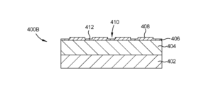
前記基板の前記第1の面をエッチングして、前記基板の前記第1の面に第1の複数の傾斜メサを形成することであって、前記第1の複数の傾斜メサの各傾斜メサは、前記垂直面に対して20度から70度の角度でエッチングされる、第1の複数の傾斜メサを形成することと、
その後、前記ハードマスク層を除去することと、
前記第1の面とは反対側の前記基板の第2の面上に、前記第1の複数の傾斜メサとは異なる角度の第2の複数の傾斜メサを形成することと、
を含む、方法。 - 前記基板の前記第1の面上に前記ハードマスク層を形成することは、化学気相堆積(CVD)、物理的気相堆積(PVD)、または原子層堆積(ALD)を使用することを含む、請求項1に記載の方法。
- 前記透明な材料がガラスまたはポリマーを含む、請求項1に記載の方法。
- 前記基板の前記第2の面上に前記第2の複数の傾斜メサを形成するのに、ナノインプリントリソグラフィが使用される、請求項1に記載の方法。
- 回折格子を形成する方法であって、
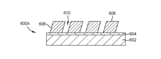
ターゲットスタック上に第1のハードマスク層を形成することであって、前記ターゲットスタックは、第1の基板の第1の面上に形成されている、第1のハードマスク層を形成することと、
前記第1のハードマスク層に複数の開口をエッチングすることと、
前記ターゲットスタックをエッチングして、前記第1の基板の前記第1の面上の前記ターゲットスタックに第1の複数の傾斜メサを形成することであって、前記第1の複数の傾斜メサの各傾斜メサは、垂直面に対して20度から70度の第1の角度でエッチングされる、第1の複数の傾斜メサを形成することと、
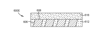
エッチングされた前記ターゲットスタックから、前記第1の基板を除去することと、
第2の基板の第1の面に、エッチングされた前記ターゲットスタックを取り付けることと、
前記第2の基板の前記第1の面とは反対側の、前記第2の基板の第2の面上に、第2のハードマスク層を形成することであって、前記第2の基板は、透明な材料を含み、前記第2の基板の幅に沿った垂直面によって規定される、第2のハードマスク層を形成することと、
前記第2のハードマスク層上に、パターニングされた層を形成することと、
前記パターニングされた層および前記第2のハードマスク層をエッチングして、前記第2の基板の前記第2の面を露出させることと、
前記パターニングされた層を除去することと、
前記第2の基板の前記第2の面をエッチングすることと、
前記エッチングに応答して、前記第2の基板の前記第2の面に第2の複数の傾斜メサを形成することであって、前記第2の複数の傾斜メサの各傾斜メサは、前記垂直面に対して20度から70度の第2の角度でエッチングされる、第2の複数の傾斜メサを形成することと、
を含む、方法。 - 前記パターニングされた層を形成することが、ナノインプリントリソグラフィを使用することを含む、請求項5に記載の方法。
- 前記第2の基板が透明基板である、請求項5に記載の方法。
- 前記ターゲットスタックは、デボンディング層を介して前記第1の基板に結合され、前記第1の基板を除去することは、前記デボンディング層を介して前記ターゲットスタックから前記第1の基板を取り外すことを含む、請求項5に記載の方法。
- 前記パターニングされた層を形成することが、ナノインプリントリソグラフィを使用することを含む、請求項8に記載の方法。
- 指向性エッチングを使用して、前記ターゲットスタックおよび前記第2の基板の前記第2の面の各々をエッチングすることをさらに含む、請求項5に記載の方法。
- 前記ターゲットスタックに対する指向性エッチングは、
前記第1の基板の前記垂直面に対して前記第1の角度をなすイオンビームの経路に前記ターゲットスタックの第1の部分を位置付けることであって、前記ターゲットスタックの前記第1の部分をエッチングすることは、前記ターゲットスタックの前記第1の部分を前記イオンビームに露出して、前記第1の角度で前記第1の複数の傾斜メサを形成することを含む、第1の部分を位置付けることと、
前記第1の基板を、前記垂直面に対して垂直な中心軸の周りに所定の回転角度まで回転させることと、
を含む、請求項10に記載の方法。 - 回折格子を形成する方法であって、
ターゲットスタック上に第1のハードマスク層を形成することであって、前記ターゲットスタックは、第1の基板の第1の面上に形成されている、第1のハードマスク層を形成することと、
前記第1のハードマスク層に複数の開口をエッチングすることと、
前記ターゲットスタックをエッチングして、前記第1の基板の前記第1の面上の前記ターゲットスタックに、第1の複数の傾斜メサを形成することであって、前記第1の複数の傾斜メサの各傾斜メサは、垂直面に対して20度から70度の角度でエッチングされる、傾斜メサを形成することと、
前記第1の面とは反対側の前記第1の基板の第2の面上に、第2のハードマスク層を形成することであって、前記第1の基板は、前記第1の基板の幅に沿った垂直面によって規定される、第2のハードマスク層を形成することと、
前記第2のハードマスク層上に、パターニングされた層を形成することと、
前記パターニングされた層および前記第2のハードマスク層をエッチングして、前記第1の基板の前記第2の面を露出させることと、
前記パターニングされた層を除去することと、
前記第1の基板の前記第2の面をエッチングすることと、
を含む方法。 - 前記パターニングされた層を形成することが、ナノインプリントリソグラフィを使用することを含む、請求項12に記載の方法。
- 前記第1の基板の前記第2の面の前記エッチングに応答して、前記第1の基板の前記第2の面に第2の複数の傾斜メサを形成することをさらに含む、請求項12に記載の方法。
- 前記第2の複数の傾斜メサの各傾斜メサは、前記垂直面に対して20度から70度の角度でエッチングされる、請求項14に記載の方法。
- 前記第1のハードマスク層および/または前記第2のハードマスク層を形成することは、化学気相堆積(CVD)、物理的気相堆積(PVD)、または原子層堆積(ALD)を使用することを含む、請求項15に記載の方法。
- 前記第1の基板が光学的に透明であり、ガラスまたはポリマーを含んでいる、請求項12に記載の方法。
Applications Claiming Priority (6)
| Application Number | Priority Date | Filing Date | Title |
|---|---|---|---|
| US201862691421P | 2018-06-28 | 2018-06-28 | |
| US62/691,421 | 2018-06-28 | ||
| US201862692286P | 2018-06-29 | 2018-06-29 | |
| US62/692,286 | 2018-06-29 | ||
| JP2020571759A JP7176013B2 (ja) | 2018-06-28 | 2019-06-27 | 回折格子の製造 |
| PCT/US2019/039615 WO2020006308A1 (en) | 2018-06-28 | 2019-06-27 | Fabrication of diffraction gratings |
Related Parent Applications (1)
| Application Number | Title | Priority Date | Filing Date |
|---|---|---|---|
| JP2020571759A Division JP7176013B2 (ja) | 2018-06-28 | 2019-06-27 | 回折格子の製造 |
Publications (2)
| Publication Number | Publication Date |
|---|---|
| JP2023022053A JP2023022053A (ja) | 2023-02-14 |
| JP7512349B2 true JP7512349B2 (ja) | 2024-07-08 |
Family
ID=68987556
Family Applications (2)
| Application Number | Title | Priority Date | Filing Date |
|---|---|---|---|
| JP2020571759A Active JP7176013B2 (ja) | 2018-06-28 | 2019-06-27 | 回折格子の製造 |
| JP2022178867A Active JP7512349B2 (ja) | 2018-06-28 | 2022-11-08 | 回折格子の製造 |
Family Applications Before (1)
| Application Number | Title | Priority Date | Filing Date |
|---|---|---|---|
| JP2020571759A Active JP7176013B2 (ja) | 2018-06-28 | 2019-06-27 | 回折格子の製造 |
Country Status (7)
| Country | Link |
|---|---|
| US (2) | US11333896B2 (ja) |
| EP (1) | EP3814840B1 (ja) |
| JP (2) | JP7176013B2 (ja) |
| KR (2) | KR102650642B1 (ja) |
| CN (2) | CN112368639B (ja) |
| TW (1) | TWI710016B (ja) |
| WO (1) | WO2020006308A1 (ja) |
Families Citing this family (18)
| Publication number | Priority date | Publication date | Assignee | Title |
|---|---|---|---|---|
| KR102650642B1 (ko) * | 2018-06-28 | 2024-03-21 | 어플라이드 머티어리얼스, 인코포레이티드 | 회절 격자들의 제조 |
| US11111176B1 (en) * | 2020-02-27 | 2021-09-07 | Applied Materials, Inc. | Methods and apparatus of processing transparent substrates |
| US11662524B2 (en) * | 2020-03-13 | 2023-05-30 | Applied Materials, Inc. | Forming variable depth structures with laser ablation |
| EP4147081B1 (en) * | 2020-05-08 | 2025-06-11 | Nil Technology ApS | Methods for manufacturing multi-level structures |
| TWI800844B (zh) * | 2020-06-02 | 2023-05-01 | 國立臺灣大學 | 超穎介面急劇自聚焦光束產生裝置 |
| KR102873571B1 (ko) * | 2020-07-09 | 2025-10-17 | 어플라이드 머티어리얼스, 인코포레이티드 | 나노구조 광학 디바이스들의 에어-갭 캡슐화 |
| US11543584B2 (en) * | 2020-07-14 | 2023-01-03 | Meta Platforms Technologies, Llc | Inorganic matrix nanoimprint lithographs and methods of making thereof with reduced carbon |
| US11487058B2 (en) | 2020-08-13 | 2022-11-01 | Applied Materials, Inc. | Method for manufacturing optical device structures |
| EP4020024A1 (en) | 2020-12-22 | 2022-06-29 | Paul Scherrer Institut | Method for producing high aspect ratio fan-shaped optics |
| WO2022193107A1 (zh) * | 2021-03-16 | 2022-09-22 | 京东方科技集团股份有限公司 | 一种透镜阵列及其制备方法 |
| EP4416540A4 (en) * | 2021-10-15 | 2025-08-13 | Applied Materials Inc | MULTILAYER TRANSMISSION STRUCTURES FOR WAVEGUIDE DISPLAY DEVICE |
| US11835763B2 (en) * | 2021-10-22 | 2023-12-05 | Northrop Grumman Systems Corporation | Nanoimprinted photonic integrated circuits |
| US11892676B2 (en) * | 2022-01-10 | 2024-02-06 | Applied Materials, Inc. | Self-aligned formation of angled optical device structures |
| WO2023205288A1 (en) * | 2022-04-20 | 2023-10-26 | Applied Materials, Inc. | Method for roughness reduction in manufacturing optical device structures |
| TW202432449A (zh) * | 2022-10-18 | 2024-08-16 | 日商東京威力科創股份有限公司 | 繞射光柵之形成方法 |
| CN115598755A (zh) * | 2022-11-07 | 2023-01-13 | 杭州探真纳米科技有限公司(Cn) | 一种高折射率斜齿光栅的制造方法 |
| KR20260027330A (ko) * | 2023-06-27 | 2026-02-27 | 어플라이드 머티어리얼스, 인코포레이티드 | 광학 디바이스 구조물들을 제작하기 위한 방법 |
| US20250067937A1 (en) * | 2023-08-25 | 2025-02-27 | Applied Materials, Inc. | Individual grating fabrication and assembly |
Citations (4)
| Publication number | Priority date | Publication date | Assignee | Title |
|---|---|---|---|---|
| JP2005004068A (ja) | 2003-06-13 | 2005-01-06 | Dainippon Printing Co Ltd | スラント凹凸パターンの形成方法及びスラント凹凸パターンを有する基板 |
| JP2005149594A (ja) | 2003-11-13 | 2005-06-09 | Ricoh Co Ltd | 偏光回折光学素子、光ピックアップ及び光ディスクドライブ装置 |
| JP2006318568A (ja) | 2005-05-12 | 2006-11-24 | Enplas Corp | 光学素子およびこれを備えた光ピックアップ装置ならびに不要光の除去方法 |
| JP2009516225A (ja) | 2005-11-18 | 2009-04-16 | ナノコンプ オイ リミテッド | 回折格子の製造方法 |
Family Cites Families (26)
| Publication number | Priority date | Publication date | Assignee | Title |
|---|---|---|---|---|
| JPH1096807A (ja) * | 1996-09-19 | 1998-04-14 | Dainippon Printing Co Ltd | ホログラフィック光学素子及びその作製方法 |
| JP3877444B2 (ja) | 1998-09-02 | 2007-02-07 | 富士通株式会社 | 回折格子 |
| US6570753B2 (en) * | 2001-05-25 | 2003-05-27 | University Of Houston | Capacitor and method of storing energy |
| JP3955066B2 (ja) * | 2002-04-03 | 2007-08-08 | 東邦エンジニアリング株式会社 | 研磨パッドと該研磨パッドの製造方法および該研磨パッドを用いた半導体基板の製造方法 |
| JP4478398B2 (ja) * | 2002-04-19 | 2010-06-09 | 株式会社リコー | 偏光光学素子、光学素子ユニット、光ヘッド装置及び光ディスクドライブ装置 |
| US7164532B2 (en) * | 2002-04-19 | 2007-01-16 | Ricoh Company, Ltd. | Diffraction grating, light source unit applying the same therein, and optical head device employing the same |
| US6716737B2 (en) * | 2002-07-29 | 2004-04-06 | Hewlett-Packard Development Company, L.P. | Method of forming a through-substrate interconnect |
| US7670758B2 (en) * | 2004-04-15 | 2010-03-02 | Api Nanofabrication And Research Corporation | Optical films and methods of making the same |
| US20050275944A1 (en) * | 2004-06-11 | 2005-12-15 | Wang Jian J | Optical films and methods of making the same |
| JP2007316270A (ja) * | 2006-05-25 | 2007-12-06 | Sony Corp | 光学部品の製造方法、位相差素子および偏光子 |
| US20100277803A1 (en) * | 2006-12-14 | 2010-11-04 | Nokia Corporation | Display Device Having Two Operating Modes |
| JP5724213B2 (ja) | 2010-05-13 | 2015-05-27 | セイコーエプソン株式会社 | 検出装置 |
| US20120257490A1 (en) * | 2011-04-07 | 2012-10-11 | Seagate Technology Llc | Gratings For Waveguide Coupling |
| KR101966622B1 (ko) | 2012-04-05 | 2019-04-09 | 삼성전자주식회사 | 나노 임프린트 리소그래피용 템플리트의 제조 및 보정 방법 |
| GB2502818A (en) * | 2012-06-08 | 2013-12-11 | Nanogan Ltd | Epitaxial growth of semiconductor material such as Gallium Nitride on oblique angled nano or micro-structures |
| CN103675969B (zh) * | 2013-12-04 | 2016-01-20 | 中国科学院上海光学精密机械研究所 | 高效率斜双层光栅 |
| US20160033784A1 (en) * | 2014-07-30 | 2016-02-04 | Tapani Levola | Optical Components |
| US20160035539A1 (en) * | 2014-07-30 | 2016-02-04 | Lauri SAINIEMI | Microfabrication |
| JPWO2016133161A1 (ja) | 2015-02-20 | 2017-11-30 | 日本碍子株式会社 | 光学素子の製造方法 |
| US9941389B2 (en) | 2015-04-20 | 2018-04-10 | Board Of Regents, The University Of Texas System | Fabricating large area multi-tier nanostructures |
| WO2018039277A1 (en) | 2016-08-22 | 2018-03-01 | Magic Leap, Inc. | Diffractive eyepiece |
| CN116520644A (zh) | 2017-11-29 | 2023-08-01 | 应用材料公司 | 波导组合器的直接蚀刻制造的方法 |
| US10845596B2 (en) * | 2018-01-23 | 2020-11-24 | Facebook Technologies, Llc | Slanted surface relief grating for rainbow reduction in waveguide display |
| US10302826B1 (en) | 2018-05-30 | 2019-05-28 | Applied Materials, Inc. | Controlling etch angles by substrate rotation in angled etch tools |
| KR102650642B1 (ko) * | 2018-06-28 | 2024-03-21 | 어플라이드 머티어리얼스, 인코포레이티드 | 회절 격자들의 제조 |
| TWI730548B (zh) * | 2018-12-17 | 2021-06-11 | 美商應用材料股份有限公司 | 用於光學設備製造的電子束裝置 |
-
2019
- 2019-06-27 KR KR1020237016781A patent/KR102650642B1/ko active Active
- 2019-06-27 WO PCT/US2019/039615 patent/WO2020006308A1/en not_active Ceased
- 2019-06-27 EP EP19824762.9A patent/EP3814840B1/en active Active
- 2019-06-27 JP JP2020571759A patent/JP7176013B2/ja active Active
- 2019-06-27 CN CN201980040608.8A patent/CN112368639B/zh active Active
- 2019-06-27 KR KR1020217002777A patent/KR102535740B1/ko active Active
- 2019-06-27 CN CN202410879867.2A patent/CN118732110A/zh active Pending
- 2019-06-27 US US16/454,642 patent/US11333896B2/en active Active
- 2019-06-28 TW TW108122812A patent/TWI710016B/zh active
-
2022
- 2022-05-16 US US17/745,457 patent/US11733533B2/en active Active
- 2022-11-08 JP JP2022178867A patent/JP7512349B2/ja active Active
Patent Citations (4)
| Publication number | Priority date | Publication date | Assignee | Title |
|---|---|---|---|---|
| JP2005004068A (ja) | 2003-06-13 | 2005-01-06 | Dainippon Printing Co Ltd | スラント凹凸パターンの形成方法及びスラント凹凸パターンを有する基板 |
| JP2005149594A (ja) | 2003-11-13 | 2005-06-09 | Ricoh Co Ltd | 偏光回折光学素子、光ピックアップ及び光ディスクドライブ装置 |
| JP2006318568A (ja) | 2005-05-12 | 2006-11-24 | Enplas Corp | 光学素子およびこれを備えた光ピックアップ装置ならびに不要光の除去方法 |
| JP2009516225A (ja) | 2005-11-18 | 2009-04-16 | ナノコンプ オイ リミテッド | 回折格子の製造方法 |
Also Published As
| Publication number | Publication date |
|---|---|
| US11733533B2 (en) | 2023-08-22 |
| US20220276498A1 (en) | 2022-09-01 |
| CN118732110A (zh) | 2024-10-01 |
| KR102535740B1 (ko) | 2023-05-26 |
| CN112368639B (zh) | 2024-07-09 |
| KR20230070541A (ko) | 2023-05-23 |
| TW202002047A (zh) | 2020-01-01 |
| KR20210016062A (ko) | 2021-02-10 |
| JP7176013B2 (ja) | 2022-11-21 |
| JP2023022053A (ja) | 2023-02-14 |
| EP3814840B1 (en) | 2025-11-05 |
| TWI710016B (zh) | 2020-11-11 |
| JP2021530862A (ja) | 2021-11-11 |
| US11333896B2 (en) | 2022-05-17 |
| EP3814840A1 (en) | 2021-05-05 |
| CN112368639A (zh) | 2021-02-12 |
| WO2020006308A1 (en) | 2020-01-02 |
| US20200004029A1 (en) | 2020-01-02 |
| EP3814840A4 (en) | 2022-03-23 |
| KR102650642B1 (ko) | 2024-03-21 |
Similar Documents
| Publication | Publication Date | Title |
|---|---|---|
| JP7512349B2 (ja) | 回折格子の製造 | |
| US7727410B2 (en) | Process for formation of three-dimensional photonic crystal | |
| US7256938B2 (en) | Method for making large scale multilayer dielectric diffraction gratings on thick substrates using reactive ion etching | |
| KR100968160B1 (ko) | 광학 소자 및 광학 소자의 제조방법 | |
| JP5644192B2 (ja) | 積層樹脂膜の形成方法及び半導体デバイスの製造方法 | |
| JP5742517B2 (ja) | サンプルドグレーティングの形成方法及び半導体レーザの製造方法 | |
| JP7474103B2 (ja) | 光学素子の製造方法、及び、光学素子 | |
| KR102873571B1 (ko) | 나노구조 광학 디바이스들의 에어-갭 캡슐화 | |
| CN117631110A (zh) | 一种掩埋型反射式全介质衍射光栅及其制备方法 | |
| CN116953864B (zh) | 一种适合激光与波导直接耦合的硅光芯片及其制造方法 | |
| KR20050112494A (ko) | 회절형 박막 압전 마이크로 미러 및 그 제조 방법 | |
| CN110426777B (zh) | 一种可实现宽频带圆偏振的耦合腔光子晶体异质结构 | |
| KR100501247B1 (ko) | 아조벤젠 물질을 이용한 에칭 마스크 | |
| JPS6314321B2 (ja) | ||
| WO2025033058A1 (ja) | 透過型回折格子およびその製造方法 | |
| TW202522051A (zh) | 製造具有二元及閃耀光柵結構的光學裝置的方法 | |
| CN121532349A (zh) | 弯曲表面上的元光学元件 | |
| CN120507826A (zh) | 光栅制作方法及光波导产品 | |
| CN117518323A (zh) | 闪耀光栅的制备方法及闪耀光栅 |
Legal Events
| Date | Code | Title | Description |
|---|---|---|---|
| A521 | Request for written amendment filed |
Free format text: JAPANESE INTERMEDIATE CODE: A523 Effective date: 20221207 |
|
| A621 | Written request for application examination |
Free format text: JAPANESE INTERMEDIATE CODE: A621 Effective date: 20221207 |
|
| A977 | Report on retrieval |
Free format text: JAPANESE INTERMEDIATE CODE: A971007 Effective date: 20231120 |
|
| A131 | Notification of reasons for refusal |
Free format text: JAPANESE INTERMEDIATE CODE: A131 Effective date: 20231128 |
|
| A521 | Request for written amendment filed |
Free format text: JAPANESE INTERMEDIATE CODE: A523 Effective date: 20240228 |
|
| TRDD | Decision of grant or rejection written | ||
| A01 | Written decision to grant a patent or to grant a registration (utility model) |
Free format text: JAPANESE INTERMEDIATE CODE: A01 Effective date: 20240528 |
|
| A61 | First payment of annual fees (during grant procedure) |
Free format text: JAPANESE INTERMEDIATE CODE: A61 Effective date: 20240626 |