JP7512349B2 - Diffraction grating manufacturing - Google Patents
Diffraction grating manufacturing Download PDFInfo
- Publication number
- JP7512349B2 JP7512349B2 JP2022178867A JP2022178867A JP7512349B2 JP 7512349 B2 JP7512349 B2 JP 7512349B2 JP 2022178867 A JP2022178867 A JP 2022178867A JP 2022178867 A JP2022178867 A JP 2022178867A JP 7512349 B2 JP7512349 B2 JP 7512349B2
- Authority
- JP
- Japan
- Prior art keywords
- substrate
- angled
- hard mask
- mesas
- forming
- Prior art date
- Legal status (The legal status is an assumption and is not a legal conclusion. Google has not performed a legal analysis and makes no representation as to the accuracy of the status listed.)
- Active
Links
Images


Classifications
-
- G—PHYSICS
- G02—OPTICS
- G02B—OPTICAL ELEMENTS, SYSTEMS OR APPARATUS
- G02B5/00—Optical elements other than lenses
- G02B5/18—Diffraction gratings
-
- G—PHYSICS
- G02—OPTICS
- G02B—OPTICAL ELEMENTS, SYSTEMS OR APPARATUS
- G02B27/00—Optical systems or apparatus not provided for by any of the groups G02B1/00 - G02B26/00, G02B30/00
- G02B27/09—Beam shaping, e.g. changing the cross-sectional area, not otherwise provided for
- G02B27/0938—Using specific optical elements
- G02B27/0944—Diffractive optical elements, e.g. gratings, holograms
-
- G—PHYSICS
- G02—OPTICS
- G02B—OPTICAL ELEMENTS, SYSTEMS OR APPARATUS
- G02B5/00—Optical elements other than lenses
- G02B5/18—Diffraction gratings
- G02B5/1847—Manufacturing methods
- G02B5/1857—Manufacturing methods using exposure or etching means, e.g. holography, photolithography, exposure to electron or ion beams
-
- G—PHYSICS
- G02—OPTICS
- G02B—OPTICAL ELEMENTS, SYSTEMS OR APPARATUS
- G02B6/00—Light guides; Structural details of arrangements comprising light guides and other optical elements, e.g. couplings
- G02B6/10—Light guides; Structural details of arrangements comprising light guides and other optical elements, e.g. couplings of the optical waveguide type
- G02B6/12—Light guides; Structural details of arrangements comprising light guides and other optical elements, e.g. couplings of the optical waveguide type of the integrated circuit kind
- G02B6/122—Basic optical elements, e.g. light-guiding paths
- G02B6/124—Geodesic lenses or integrated gratings
-
- G—PHYSICS
- G02—OPTICS
- G02B—OPTICAL ELEMENTS, SYSTEMS OR APPARATUS
- G02B6/00—Light guides; Structural details of arrangements comprising light guides and other optical elements, e.g. couplings
- G02B6/10—Light guides; Structural details of arrangements comprising light guides and other optical elements, e.g. couplings of the optical waveguide type
- G02B6/12—Light guides; Structural details of arrangements comprising light guides and other optical elements, e.g. couplings of the optical waveguide type of the integrated circuit kind
- G02B6/13—Integrated optical circuits characterised by the manufacturing method
- G02B6/136—Integrated optical circuits characterised by the manufacturing method by etching
-
- G—PHYSICS
- G03—PHOTOGRAPHY; CINEMATOGRAPHY; ANALOGOUS TECHNIQUES USING WAVES OTHER THAN OPTICAL WAVES; ELECTROGRAPHY; HOLOGRAPHY
- G03F—PHOTOMECHANICAL PRODUCTION OF TEXTURED OR PATTERNED SURFACES, e.g. FOR PRINTING, FOR PROCESSING OF SEMICONDUCTOR DEVICES; MATERIALS THEREFOR; ORIGINALS THEREFOR; APPARATUS SPECIALLY ADAPTED THEREFOR
- G03F1/00—Originals for photomechanical production of textured or patterned surfaces, e.g., masks, photo-masks, reticles; Mask blanks or pellicles therefor; Containers specially adapted therefor; Preparation thereof
- G03F1/68—Preparation processes not covered by groups G03F1/20 - G03F1/50
- G03F1/80—Etching
-
- G—PHYSICS
- G03—PHOTOGRAPHY; CINEMATOGRAPHY; ANALOGOUS TECHNIQUES USING WAVES OTHER THAN OPTICAL WAVES; ELECTROGRAPHY; HOLOGRAPHY
- G03F—PHOTOMECHANICAL PRODUCTION OF TEXTURED OR PATTERNED SURFACES, e.g. FOR PRINTING, FOR PROCESSING OF SEMICONDUCTOR DEVICES; MATERIALS THEREFOR; ORIGINALS THEREFOR; APPARATUS SPECIALLY ADAPTED THEREFOR
- G03F7/00—Photomechanical, e.g. photolithographic, production of textured or patterned surfaces, e.g. printing surfaces; Materials therefor, e.g. comprising photoresists; Apparatus specially adapted therefor
- G03F7/0002—Lithographic processes using patterning methods other than those involving the exposure to radiation, e.g. by stamping
-
- G—PHYSICS
- G03—PHOTOGRAPHY; CINEMATOGRAPHY; ANALOGOUS TECHNIQUES USING WAVES OTHER THAN OPTICAL WAVES; ELECTROGRAPHY; HOLOGRAPHY
- G03F—PHOTOMECHANICAL PRODUCTION OF TEXTURED OR PATTERNED SURFACES, e.g. FOR PRINTING, FOR PROCESSING OF SEMICONDUCTOR DEVICES; MATERIALS THEREFOR; ORIGINALS THEREFOR; APPARATUS SPECIALLY ADAPTED THEREFOR
- G03F7/00—Photomechanical, e.g. photolithographic, production of textured or patterned surfaces, e.g. printing surfaces; Materials therefor, e.g. comprising photoresists; Apparatus specially adapted therefor
- G03F7/20—Exposure; Apparatus therefor
- G03F7/2022—Multi-step exposure, e.g. hybrid; backside exposure; blanket exposure, e.g. for image reversal; edge exposure, e.g. for edge bead removal; corrective exposure
-
- H—ELECTRICITY
- H10—SEMICONDUCTOR DEVICES; ELECTRIC SOLID-STATE DEVICES NOT OTHERWISE PROVIDED FOR
- H10P—GENERIC PROCESSES OR APPARATUS FOR THE MANUFACTURE OR TREATMENT OF DEVICES COVERED BY CLASS H10
- H10P14/00—Formation of materials, e.g. in the shape of layers or pillars
- H10P14/60—Formation of materials, e.g. in the shape of layers or pillars of insulating materials
- H10P14/63—Formation of materials, e.g. in the shape of layers or pillars of insulating materials characterised by the formation processes
- H10P14/6326—Deposition processes
- H10P14/6328—Deposition from the gas or vapour phase
- H10P14/6329—Deposition from the gas or vapour phase using physical ablation of a target, e.g. physical vapour deposition or pulsed laser deposition
-
- H—ELECTRICITY
- H10—SEMICONDUCTOR DEVICES; ELECTRIC SOLID-STATE DEVICES NOT OTHERWISE PROVIDED FOR
- H10P—GENERIC PROCESSES OR APPARATUS FOR THE MANUFACTURE OR TREATMENT OF DEVICES COVERED BY CLASS H10
- H10P14/00—Formation of materials, e.g. in the shape of layers or pillars
- H10P14/60—Formation of materials, e.g. in the shape of layers or pillars of insulating materials
- H10P14/63—Formation of materials, e.g. in the shape of layers or pillars of insulating materials characterised by the formation processes
- H10P14/6326—Deposition processes
- H10P14/6328—Deposition from the gas or vapour phase
- H10P14/6334—Deposition from the gas or vapour phase using decomposition or reaction of gaseous or vapour phase compounds, i.e. chemical vapour deposition
- H10P14/6339—Deposition from the gas or vapour phase using decomposition or reaction of gaseous or vapour phase compounds, i.e. chemical vapour deposition deposition by cyclic CVD, e.g. ALD, ALE or pulsed CVD
-
- H—ELECTRICITY
- H10—SEMICONDUCTOR DEVICES; ELECTRIC SOLID-STATE DEVICES NOT OTHERWISE PROVIDED FOR
- H10P—GENERIC PROCESSES OR APPARATUS FOR THE MANUFACTURE OR TREATMENT OF DEVICES COVERED BY CLASS H10
- H10P50/00—Etching of wafers, substrates or parts of devices
-
- H—ELECTRICITY
- H10—SEMICONDUCTOR DEVICES; ELECTRIC SOLID-STATE DEVICES NOT OTHERWISE PROVIDED FOR
- H10P—GENERIC PROCESSES OR APPARATUS FOR THE MANUFACTURE OR TREATMENT OF DEVICES COVERED BY CLASS H10
- H10P76/00—Manufacture or treatment of masks on semiconductor bodies, e.g. by lithography or photolithography
- H10P76/40—Manufacture or treatment of masks on semiconductor bodies, e.g. by lithography or photolithography of masks comprising inorganic materials
- H10P76/408—Manufacture or treatment of masks on semiconductor bodies, e.g. by lithography or photolithography of masks comprising inorganic materials characterised by their sizes, orientations, dispositions, behaviours or shapes
- H10P76/4085—Manufacture or treatment of masks on semiconductor bodies, e.g. by lithography or photolithography of masks comprising inorganic materials characterised by their sizes, orientations, dispositions, behaviours or shapes characterised by the processes involved to create the masks
Landscapes
- Physics & Mathematics (AREA)
- General Physics & Mathematics (AREA)
- Optics & Photonics (AREA)
- Engineering & Computer Science (AREA)
- Microelectronics & Electronic Packaging (AREA)
- Manufacturing & Machinery (AREA)
- Diffracting Gratings Or Hologram Optical Elements (AREA)
- Optical Integrated Circuits (AREA)
- Exposure Of Semiconductors, Excluding Electron Or Ion Beam Exposure (AREA)
- Exposure And Positioning Against Photoresist Photosensitive Materials (AREA)
- Shaping Of Tube Ends By Bending Or Straightening (AREA)
Description
[0001] 本開示の実施形態は、概して、種々のタイプの導波路で使用されるような光学素子構造、および光学素子構造を製造するシステムならびに方法に関する。 [0001] Embodiments of the present disclosure generally relate to optical element structures for use in various types of waveguides, and systems and methods for manufacturing optical element structures.
関連技術の説明
[0002] 導波路は、信号の拡がりを1次元または2次元に制限し、最小のエネルギー損失での信号の伝播を可能にすることによって、電磁波または音波を導く構造である。波は3次元的に伝播し、音波や電磁波などの波の生成源から伝播して離れるにつれて、波は出力を失うことがある。波が1次元または2次元で伝搬するように波を閉じ込めることによって、波の出力は保存される。導波路はこのように、波が伝搬する間、波の出力を保持する。
2. Description of the Related Art A waveguide is a structure that guides electromagnetic or acoustic waves by restricting the spread of the signal to one or two dimensions, allowing the signal to propagate with minimal energy loss. Waves propagate in three dimensions, and as they propagate away from the source of the wave, such as an acoustic or electromagnetic wave, they can lose power. By confining the wave to propagate in one or two dimensions, the power of the wave is preserved. A waveguide thus retains the power of the wave as it propagates.
[0003] 導波路結合器は、複数の入力信号を受け入れ、入力信号の組み合わせである単一の出力信号を生成することによって、RF信号などの信号を組み合わせるために使用される。導波路に対する需要が増大するにつれて、例えば、光ファイバ用途、レーダ用途、科学的計装、および拡張現実において、導波路に対する需要が増大しており、現在の技術は、格子を形成するためのマスターパターンの作製およびインプリント複製の実行を包含するもので、インプリント可能な材料のみが導波路製造に使用可能である。 [0003] Waveguide couplers are used to combine signals, such as RF signals, by accepting multiple input signals and generating a single output signal that is a combination of the input signals. As the demand for waveguides increases, for example in fiber optic applications, radar applications, scientific instrumentation, and augmented reality, current technology involves creating a master pattern to form a grating and performing an imprint replication, and only imprintable materials can be used for waveguide fabrication.
[0004] そのため、改良された導波路製造のシステムおよび方法が依然として必要とされている。 [0004] Thus, there remains a need for improved waveguide manufacturing systems and methods.
[0005] 本明細書に記載のシステムおよび方法は、格子を形成する方法を対象としている。一実施例では、基板をパターニングする方法は、基板の第1の面上にハードマスク層を形成することであって、基板が透明な材料から形成され、基板の幅に沿った垂直面によって規定される、ハードマスク層を形成することと、ナノインプリントリソグラフィによって、ハードマスク層上にパターニングされた層を形成することとを含む。この実施例では、本方法は、パターニングされた層およびハードマスク層をエッチングして、基板の第1の面を露出することと、パターニングされた層を除去することと、基板の第1の面をエッチングして、基板の第1の面に第1の複数の傾斜メサ(angled mesas)を形成することとをさらに含む。第1の複数の傾斜メサの各傾斜メサは、垂直面に対して20度から70度の角度でエッチングされる。さらにこの方法では、基板の第1の面をエッチングした後、ハードマスク層を除去する。 [0005] The systems and methods described herein are directed to a method of forming a grating. In one embodiment, a method of patterning a substrate includes forming a hard mask layer on a first side of a substrate, the substrate being formed from a transparent material and defined by a vertical plane along a width of the substrate, and forming a patterned layer on the hard mask layer by nanoimprint lithography. In this embodiment, the method further includes etching the patterned layer and the hard mask layer to expose the first side of the substrate, removing the patterned layer, and etching the first side of the substrate to form a first plurality of angled mesas on the first side of the substrate. Each angled mesa of the first plurality of angled mesas is etched at an angle between 20 degrees and 70 degrees relative to the vertical plane. The method further includes removing the hard mask layer after etching the first side of the substrate.
[0006] 別の実施例では、格子を形成する方法は、第1の基板の第1の面上に形成されるターゲットスタック上にハードマスク層を形成することと、ハードマスク層内の複数の開口をエッチングすることと、ターゲットスタックをエッチングして、第1の基板の第1の面上のターゲットスタック内に第1の複数の傾斜メサを形成することとを含む。第1の複数の傾斜メサの各傾斜メサは、垂直面に対して20度から70度の第1の角度でエッチングされる。 [0006] In another embodiment, a method of forming a grating includes forming a hard mask layer on a target stack formed on a first surface of a first substrate, etching a plurality of openings in the hard mask layer, and etching the target stack to form a first plurality of angled mesas in the target stack on the first surface of the first substrate. Each angled mesa of the first plurality of angled mesas is etched at a first angle between 20 degrees and 70 degrees with respect to vertical.
[0007] 別の実施例では、格子を形成する方法は、第1の基板の第1の面上に形成されるターゲットスタック上にハードマスク層を形成することと、ハードマスク層内の複数の開口をエッチングすることと、ターゲットスタックをエッチングして、第1の基板の第1の面上のターゲットスタック内に第1の複数の傾斜メサを形成することとを含む。複数の傾斜メサの各傾斜メサは、垂直面に対して20度から70度の角度でエッチングされる。本方法はさらに、基板の幅に沿った垂直面によって規定される第1の基板の第2の面上にハードマスク層を形成することと、ナノインプリントリソグラフィによって、ハードマスク層上にパターニングされた層を形成することとを含む。 [0007] In another embodiment, a method of forming a grating includes forming a hard mask layer on a target stack formed on a first side of a first substrate, etching a plurality of openings in the hard mask layer, and etching the target stack to form a first plurality of angled mesas in the target stack on the first side of the first substrate. Each angled mesa of the plurality of angled mesas is etched at an angle of 20 degrees to 70 degrees relative to a vertical plane. The method further includes forming a hard mask layer on a second side of the first substrate defined by a vertical plane along a width of the substrate, and forming a patterned layer on the hard mask layer by nanoimprint lithography.
[0008] 本開示の上述の特徴を詳細に理解しうるように、上記で簡単に要約された本開示のより具体的な説明が、実施形態を参照することによって得られ、一部の実施形態は、添付の図面に例示されている。しかしながら、添付図面は例示的な実施形態のみを示すものであり、したがって、本開示の範囲を限定すると見なすべきではなく、その他の等しく有効な実施形態も許容されうることに留意されたい。 [0008] So that the above-mentioned features of the present disclosure may be understood in detail, a more particular description of the present disclosure briefly summarized above may be obtained by reference to embodiments, some of which are illustrated in the accompanying drawings. It should be noted, however, that the accompanying drawings show only exemplary embodiments and therefore should not be considered as limiting the scope of the present disclosure, as other equally effective embodiments may be permissible.
[0021] 理解を容易にするために、可能な場合には、図に共通する同一の要素を指し示すのに同一の参照番号を使用した。一実施形態の要素および特徴は、さらなる記述がなくても、他の実施形態に有益に組み込むことができると考えられている。 [0021] For ease of understanding, wherever possible, identical reference numbers have been used to designate identical elements common to the figures. It is believed that elements and features of one embodiment may be beneficially incorporated in other embodiments without further description.
[0022] 本明細書で説明されているシステムおよび方法は、導波路に使用される回折格子の大量生産を含むことができる。拡張現実表面レリーフ導波路結合器は、マスタリングおよび複製のプロセスによって作製される。現在、これらの導波路結合器は数千の単位でしか製造されていないが、将来的に予測される数量は数千万以上の単位となる。現在の製造プロセスにおける課題には、特に大量生産におけるように、複製された形状の再現性を含み、ナノインプリントリソグラフィ(NIL)プロセスにおける歩留まりに関する懸念が含まれる。さらに、格子が垂直面に対して45度以上の角度で形成され得るので、高角度格子のNILインプリント後の取り外しも課題となる。 [0022] The systems and methods described herein can include mass production of the diffraction gratings used in the waveguides. The augmented reality surface relief waveguide couplers are fabricated by a process of mastering and replication. Currently, these waveguide couplers are manufactured in the thousands, but future projected quantities are in the tens of millions or more. Challenges in current manufacturing processes include repeatability of the replicated features, especially in mass production, and concerns regarding yield in nanoimprint lithography (NIL) processes. Additionally, removal of high angle gratings after NIL imprinting is also a challenge, as the gratings can be formed at angles of 45 degrees or more to the vertical plane.
[0023] 本明細書で説明されるように、低い屈折率を有する材料である「低屈折率」材料は、二酸化ケイ素(SiO2)、ドープされたSiO2、フッ素化ポリマー、または多孔質材料を含み得る。高い屈折率を有する材料である「高屈折率」材料は、アモルファスおよび結晶性Si、窒化ケイ素(SiN)、二酸化チタン(TiO2)、リン酸ガリウム(GaP)、五酸化タンタル(Ta2O5)、または硫化材料およびポリマーを含み得る。 [0023] As described herein, "low index" materials, which are materials having a low refractive index, may include silicon dioxide ( SiO2 ), doped SiO2 , fluorinated polymers, or porous materials. "High index" materials, which are materials having a high refractive index, may include amorphous and crystalline Si, silicon nitride (SiN), titanium dioxide ( TiO2 ), gallium phosphate (GaP), tantalum pentoxide ( Ta2O5 ), or sulfide materials and polymers.
[0024] 本明細書で説明するのは、直接エッチングおよびNILを使用して導波路デバイスを製造するためのシステムおよび方法である。導波路結合器を含む導波路デバイスは、低屈折率材料、高屈折率材料、または低屈折率材料と高屈折率材料との組合せに形成された複数の回折格子と、ポリマーまたはガラスなどの光学的に透明な基板に形成された複数の格子とを含む。本明細書で説明しているように、「透明」基板は、導波路結合器が動作することが意図される所定の波長範囲において光学的に透明な基板である。本明細書で説明しているように、回折格子は、「格子」とも称されるが、歯またはフィンとも称される複数の傾斜メサと、隣接する傾斜メサ間に形成される複数のトラフ(溝)とを含み得る。いくつかの実施例では、格子のトラフは、充填材料を含まず、他の実施例では、格子のトラフは、様々な材料で充填される。一実施例では、格子のメサは低屈折率材料から形成することができ、格子のトラフは高屈折率材料で充填される。別の実施例では、格子の傾斜メサは、高屈折率材料から形成することができ、格子のトラフは、低屈折率材料で充填される。格子内の傾斜メサおよびトラフは、基板の垂直面に対して幅、長さ、間隔、または角度のうちの1つまたは複数において均一になり得る。別の実施例では、格子の傾斜メサおよびトラフは、基板の垂直面に対して幅、長さ、間隔、または角度のうちの1つまたは複数において異なり得る。 [0024] Described herein are systems and methods for fabricating waveguide devices using direct etching and NIL. A waveguide device including a waveguide coupler includes a plurality of diffraction gratings formed in a low refractive index material, a high refractive index material, or a combination of low and high refractive index materials, and a plurality of gratings formed in an optically transparent substrate, such as a polymer or glass. As described herein, a "transparent" substrate is a substrate that is optically transparent in the predetermined wavelength range in which the waveguide coupler is intended to operate. As described herein, a diffraction grating, also referred to as a "grating," may include a plurality of angled mesas, also referred to as teeth or fins, and a plurality of troughs (grooves) formed between adjacent angled mesas. In some embodiments, the troughs of the grating do not include a fill material, and in other embodiments, the troughs of the grating are filled with various materials. In one embodiment, the mesas of the grating can be formed from a low refractive index material, and the troughs of the grating are filled with a high refractive index material. In another example, the angled mesas of the grating can be formed from a high index material, and the troughs of the grating are filled with a low index material. The angled mesas and troughs in the grating can be uniform in one or more of width, length, spacing, or angle with respect to the vertical plane of the substrate. In another example, the angled mesas and troughs of the grating can vary in one or more of width, length, spacing, or angle with respect to the vertical plane of the substrate.
[0025] 本明細書の様々な実施形態で説明されるように、NILは直接エッチングと共に使用して、導波路結合器を製造することができる。いくつかの実施例では、両面処理法を使用して導波路結合器を製造する。両面製造法は、透明基板上にNILを使用することによって、低屈折率材料または高屈折率材料のうちの少なくとも1つから形成されるターゲットスタック内に第1の格子を形成することと、同じ基板の他方の面に直接エッチングを使用して第2の格子を形成することとを含む。直接エッチングにおける課題の1つは、ガラス基板上にリソグラフィを行うことである。例えば、従来のリソグラフィ処理は、リソグラフィスキャナパラメータにより、最大厚さ775μmの基板を受け入れるように構成することができる。導波路結合器は、現在、設計に応じた厚さを有するガラス基板を使用して作製されているが、典型的には、0.5mmまたは0.8mmの厚さであり、これは、リソグラフィスキャナが処理するように構成されているものよりも著しく薄い。 [0025] As described in various embodiments herein, NIL can be used in conjunction with direct etching to fabricate waveguide couplers. In some examples, a double-sided processing method is used to fabricate the waveguide couplers. The double-sided manufacturing method involves using NIL on a transparent substrate to form a first grating in a target stack formed from at least one of a low or high refractive index material, and using direct etching to form a second grating on the other side of the same substrate. One of the challenges with direct etching is performing lithography on glass substrates. For example, conventional lithography processes can be configured to accept substrates up to 775 μm thick, depending on the lithography scanner parameters. Waveguide couplers are currently fabricated using glass substrates with thicknesses depending on the design, but typically 0.5 mm or 0.8 mm thick, which is significantly thinner than what lithography scanners are configured to process.
[0026] 一実施形態では、格子は、シリコンから形成することができる一時的な基板上にNILおよび直接エッチングを使用して形成される。次いで、格子は、一時的な基板から剥離され、ガラスを含み得る第2の透明基板に転写される。別の実施形態では、格子は、NILを介して形成され、ガラスまたは他の透明基板上に配置済みのターゲット層上に直接エッチングされる。また、NILおよび透明基板での直接エッチングを使用して格子を形成することができる。本明細書で説明されているシステムおよび方法を使用して、高角度格子が形成され、その角度は、基板に平行な垂直面から20度から70度の範囲とすることができる。本明細書で説明される導波路および導波路構成要素は、デバイスの直接エッチングによって形成され、NILと組み合わせて、一時的な結合または永続的な結合を使用して製造することができる。 [0026] In one embodiment, the grating is formed using NIL and direct etching on a temporary substrate, which may be formed from silicon. The grating is then peeled off from the temporary substrate and transferred to a second transparent substrate, which may include glass. In another embodiment, the grating is formed via NIL and etched directly onto a target layer already disposed on a glass or other transparent substrate. Also, gratings can be formed using NIL and direct etching on a transparent substrate. Using the systems and methods described herein, high angle gratings are formed, and the angles can range from 20 degrees to 70 degrees from a normal plane parallel to the substrate. The waveguides and waveguide components described herein can be formed by direct etching of the device and fabricated using temporary or permanent bonding in combination with NIL.
[0027] 他の実施例では、広範囲のデューティサイクル(DC)(すなわち、メサピッチに対するメサ幅の比率)を有する導波路設計が望ましい。インプリント材料の収縮により、この範囲のデューティサイクルをNILで製造することは困難であろう。しかしながら、いくつかの実施形態では、この課題は、低屈折率かつ低デューティサイクル格子をインプリントし、次いで、高屈折率材料で低デューティサイクル格子を充填し、高デューティサイクルおよび高屈折率格子で格子を形成することによって克服される。 [0027] In other examples, a waveguide design with a wide range of duty cycles (DC) (i.e., ratio of mesa width to mesa pitch) is desirable. This range of duty cycles would be difficult to fabricate with NIL due to shrinkage of the imprint material. However, in some embodiments, this challenge is overcome by imprinting a low index and low duty cycle grating, then filling the low duty cycle grating with a high index material, and forming a grating with a high duty cycle and high index grating.
[0028] 図1は、透明基板上に格子構造を直接形成する方法100のフロー図である。図2A~図2Fは、方法100の操作の部分概略図である。図1および図2A~図2Fは、以下に共に参照される。
[0028] FIG. 1 is a flow diagram of a
[0029] 方法100の操作102では、図2Aの構造200Aに示すように、ターゲットスタック204が基板202上に形成される。基板202は、ガラスまたはポリマー基板などの透明基板から形成することができ、これらは0.5mmから0.8mmで形成され得る。操作104では、図2Aに示すように、ハードマスク層206がターゲットスタック204上に形成される。ターゲットスタック204は、SiN、TiO2、GaP、または別の高屈折率材料で製造することができ、操作102で、CVD、PVD、スピニングオン、または別の適切な方法によって堆積される。一実施形態では、ターゲットスタック204の厚さは、完成した導波路結合器デバイスにおいて使用される屈折率および光波長に応じて、100nmから500nmまでとすることができる。ハードマスク層206は、操作104において、TiN、TaN、Cr、またはCVD、PVD、ALD、または別の薄膜堆積処理によって堆積された別のエッチング耐性材料から製造することができる。ハードマスク層206は、操作104で、約10nmから約50nmの厚さに形成することができる。いくつかの実施例では、25nm未満の厚さのハードマスク層206を採用して、その後のエッチング操作中のシャドウイングを低減または回避することができる。
[0029] In
[0030] 方法100の操作106では、図2Bの構造200Bに示したように、NILを使用してハードマスク層206上にパターン層208が形成される。パターン層208は、インプリント可能なレジスト材料から形成される。パターン層は、複数の隆起フィーチャ210から形成され、複数のギャップ212が、隣接する隆起フィーチャ210のペアの間に形成される。複数のギャップ212の各ギャップは、パターン層208の底部残留層214を有する。一実施形態では、操作106において、ハードマスクのNILは、隆起フィーチャ210の各々と基板202との間の角度δで実行される。角度δは、90度よりも大きくすることができ、これは、本明細書で説明するように、コストを低下させ、指向性エッチング中に後続のフィーチャの形成を促進することができる。
[0030] In
[0031] 続いて、操作108において、および図2Cの構造200Cに示したように、ハードマスク層206およびパターン層208の一部は、エッチングによって除去される。このように、各ギャップ212の底部216がターゲットスタック204を露出し、複数のハードマスクメサ218が形成される。方法100の操作110において、図2Dの構造200Dに示したように、パターン層208が除去され、複数のハードマスクメサ218を露出させる。操作112では、図2Eの構造200Eに示したように、ターゲットスタック204がエッチングされて、複数の傾斜メサ222と、傾斜メサ222の間に複数のトラフ220が形成され、操作112でのエッチングによって、基板202が露出される。複数の傾斜メサ222は、基板202の垂直面224から角度αで形成することができる。操作112でのエッチングは、指向性エッチングと呼ぶことができる。角度αは、20度から70度とすることができる。
[0031] Subsequently, in
[0032] 操作114では、図2Fの構造200Fに示したように、ハードマスク層206の残りの部分が除去され、複数の傾斜メサ222および複数のトラフ220が深さ226まで形成されたまま残される。本明細書で説明されている指向性エッチングは、一実施例では、エッチングチャンバ内のイオンビームの経路の第1の位置に、プラテン上に保持される基板202の第1の部分を配置することによって実行される。イオンビームは、リボンビーム、スポットビーム、または第1のエッジから第1のエッジに平行な第2のエッジまで基板を横切って延在する完全な基板サイズのビームとすることができる。イオンビームは、ターゲットスタック204などのターゲット材料の上面に接触するように構成され、傾斜メサ222を含む第1の格子を形成する。イオンビーム角度は、0度から90度(すなわち、所望の任意の角度)になり得るが、イオンビームは、典型的には、イオンビームが所望の最大角度でターゲットスタック204をアタックするように、基板202の垂直面に対して所望のエッチング角度(例えば、20度から70度)に設定される。イオンビーム方向によって設定される最大角度よりも低い角度を有するエッチングを得るために、プラテン上に保持された基板202は、プラテンの軸を中心として所定の回転角度まで回転させることができる。回転の結果、イオンビームがターゲットスタック204の上面に異なる角度で接触し、第2の格子または他の後続の格子を形成する。基板の回転量、例えば、使用される所定の回転角度を計算して、所望の正確な格子エッチング角度を生成することができる。
[0032] In
[0033] 代替の実施形態では、操作112での指向性エッチングは、本明細書で説明されている種々の格子にわたるハードマスク厚を調整することによって、制御(例えば、エッチング深さ、エッチング角度、およびエッチング速度の制御)可能である。ハードマスク厚の調整は、ハードマスクのエッチングおよび/またはNILによって達成することができ、いくつかの実施例では、NILは、より費用対効果の高いものとなり得る。この実施例では、操作112での指向性エッチングが実行されるとき、図2Fの226によって示されるような複数のトラフ220の最終的な深さは、格子上の異なる位置で(操作106でNILによって形成される)ハードマスク層206の厚さに応じて変化し得る。
[0033] In an alternative embodiment, the directional etching in
[0034] 図3は、透明基板上に格子構造を直接形成する方法300のフロー図である。図4A~図4Eは、方法300の部分概略図である。図3および図4A~図4Eは共に、以下に説明される。
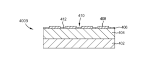
[0034] FIG. 3 is a flow diagram of a
[0035] 方法300の操作302では、図4Aの構造400Aに示したように、ターゲットスタック404が基板402上に形成される。基板402は透明であり、ポリマー、ガラス、セラミック、または他の光学的に透明な材料から形成することができる。ターゲットスタック404は、化学気相成長(CVD)によって100nmから500nmの厚さに形成される。代替的な実施形態では、PVD、スピニングオン、またはALDを使用して、ターゲットスタック404を形成することができる。操作304では、図4Bの構造400Bに示したように、ターゲットスタック404上にNILを介してハードマスク406が形成される。ハードマスク406は、フィーチャ408と、隣接するフィーチャ408間のギャップ410との層として形成される。各ギャップ410の底部412は、その上に形成されるハードマスク406を有する。ハードマスク406は、金属または金属酸化物、TiNまたはTaNを含む金属窒化物、炭素から、あるいは別のエッチング耐性ナノインプリント可能材料から製造することができる。操作306では、図4Cの構造400Cに示したように、各ギャップ410内のハードマスク406の下部412層は、エッチングを介して除去され、ターゲットスタック404を露出させる。操作308では、図4Dの構造400Dに示したように、ターゲットスタック404は、複数の傾斜メサ414を形成するようにエッチングされる。複数の傾斜メサ414は、基板402の垂直面418から角度αで形成することができる。角度αは、20度から70度とすることができる。複数の傾斜メサ414の各々は、同様の幅420で図4Dに示されているが、他の実施例では、傾斜メサ414の間の幅またはその他の寸法は、角度αを含め、変化し得る。傾斜メサ414は、ターゲットスタック404に対してある角度でエッチャントを向けるように構成されたツーリングを用いた指向性エッチングによって形成することができる。操作310では、図4Eの構造400Eに示したように、ハードマスク406が除去される。方法300は、第1の操作でハードマスクが堆積され、次いで第2の操作でパターニングされる本明細書で説明される方法とは対照的に、操作304でハードマスク406を形成することが望ましい場合に使用することができる。
[0035] In
[0036] 図5は、本開示の実施形態による、第1の基板から第2の基板に格子構造を転写する方法500である。図6A~図6Eは、方法500の部分概略図である。図5および図6A~図6Eは、以下で共に説明される。
[0036] FIG. 5 is a
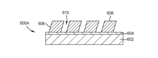
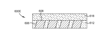
[0037] 図6Aは、上述の図1の方法100および図3の方法300にしたがって製造された構造と同様に製造された構造を示す。しかしながら、図6Aは、上述のように透明基板上に形成される代わりに、シリコンを含む第1の基板602上に形成された格子606を含む構造600Aを示す。デボンディング層604は、CVDを使用して二酸化ケイ素の薄い層を成長させることによって、または第1の基板602と格子606との間の薄い接着剤上でスピニングすることによって形成される。格子606は、複数の傾斜メサ608と、隣接する傾斜メサ608の各ペア間の複数のトラフ610とを含む。第1の基板602は、シリコンから形成することができる。本明細書の他の実施例と組み合わせることができる別の実施例では、格子606は、高屈折率材料から形成することができ、デボンディング層604は、熱応答性接着剤またはSiO2の層から形成することができる。方法500の操作502では、図6Aの構造がプロセスチャンバ内に受け入れられる。操作504では、充填層612が、図6Bの構造600Bに示したように、トラフ610内および格子606の傾斜メサ608の上に堆積される。いくつかの実施例では、操作504中に、充填層612は、傾斜メサ608の上部に層614を形成する。低屈折率材料のこの層614は、図6Cの構造600Cに示したように、機械的手段、化学的手段、またはこれらの組み合わせを介して、操作506で除去される。図6Dの構造600Dに示した操作508において、構造600Dは、第1の基板602が結合された場所とは反対側のガラス基板618に結合される。図6Eの構造600Eに示した操作510では、第1の基板602は、デボンディング層604が格子606から解放されるように、熱手段を介して除去されるか、またはシリコンウェハを研磨してSiO2上に停止させることによって除去される。
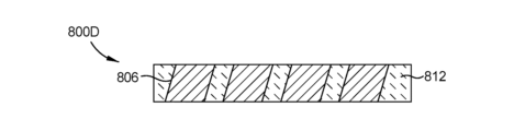
[0037] Figure 6A shows a structure manufactured similarly to the structures manufactured according to the
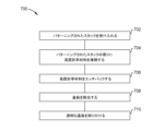
[0038] 図7は、本開示の実施形態による、第1の基板から第2の基板に格子構造を転写する方法700である。図8A~図8Eは、方法700の部分概略図である。図7および図8A~図8Eは、以下で共に参照される。
[0038] FIG. 7 is a
[0039] 図8Aは、上述の図1の方法100および図3の方法300にしたがって製造された構造と同様に製造された構造800Aを示す。しかしながら、図8Aは、上述のように透明基板上に形成される代わりに、第1の基板802上に形成された格子806を示す。一実施例では、第1の基板802はシリコンから形成される。デボンディング層804は、第1の基板802と格子806との間に形成される。格子806は、複数の傾斜メサ808と、傾斜メサ808の間にある複数のトラフ810とを備える。一実施例では、第1の基板802は、シリコンから形成することができる。本明細書の他の実施例と組み合わせることができる別の実施例では、格子806は、低屈折率材料から形成することができる。デボンディング層804は、熱応答性接着剤から形成することができる。方法700の操作702では、図8Aの構造が処理チャンバ内に受け入れられる。操作704では、図8Bの構造800Bに示したように、充填層812が、トラフ810内および格子806の傾斜メサ608の上に堆積される。いくつかの実施例では、操作704中に、充填層812は、傾斜メサ808の上部に層814を含む。高屈折率材料のこの層814は、図8Cの構造800Cに示したように、機械的手段、化学的手段、またはこれらの組み合わせを介して、操作706で除去される。操作708では、図8Dの構造800Dに示したように、第1の基板802は、デボンディング層804が格子806から取り外されるように、熱手段によって除去される。操作710では、図8Eの構造800Eに示したように、図8Dの構造800Dは、第1の基板802が結合された側とは反対側のガラス基板818に結合される。
[0039] FIG. 8A illustrates a
[0040] 図9は、透明基板に格子構造を直接エッチングする方法900である。図10A~図10Fは、方法900の部分概略図である。図9および図10A~図10Fは、以下で共に参照される。
[0040] FIG. 9 is a
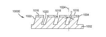
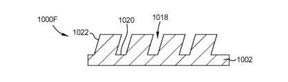
[0041] 方法900では、図10Aの構造1000Aに示したように、操作902で、ハードマスク1004が透明基板1002上に形成される。透明基板1002は、ガラス、ポリマー、または光学的に透明な他の材料から形成することができる。ハードマスク1004は、TiN、TaN、Cr、または他のエッチング耐性材料から形成することができ、操作902において、CVD、PVD、ALD、または他の方法を介して、10nmから50nmの厚さで形成される。操作904では、図10Bの構造1000Bに示したように、層1006を生成するため、NILによってパターンが形成される。層1006は、複数のメサ1010およびトラフ1012として形成される。各トラフ1012の底部1008は、層1006の材料の残留層から形成される。層1006は、実施形態に応じて、低屈折率材料または高屈折率材料とすることができる。層1006は、図10Cに示した構造1000Cを形成するため、操作906で、ハードマスク1004と共にエッチングされる。操作906で層1006およびハードマスク1004をエッチングすることによって、トラフ1012の底部1014において透明基板1002が露出される。操作908では、図10Dの構造1000Dに示したように、層1006が除去され、複数のハードマスクアイランド1016が残る。操作910では、図10Eの構造1000に示したように、透明基板1002は、エッチングされて、複数の傾斜メサ1022を形成し、複数のトラフ1018は、各隣接する傾斜メサ1022のペア間に形成される。複数の傾斜メサ1022の各傾斜メサ1022は、垂直面1024からαの角度にある。各トラフ1018の底部1020は、基板材料である。操作912では、図10Fに示したように、ハードマスク1004が除去され、ハードマスクアイランド1016が除去され、透明基板1002の構造1000Fが残される。
[0041] In
[0042] 図11A~図11Cは、本開示の実施形態による導波路結合器を製造するために使用される方法のフロー図である。 [0042] Figures 11A-11C are flow diagrams of a method used to fabricate a waveguide coupler according to an embodiment of the present disclosure.
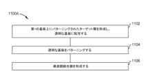
[0043] 図11Aは、本開示の実施形態による、導波路結合器において使用可能な回折格子を形成する方法1100Aを示す。操作1102では、シリコン(Si)から形成され得る第1の基板に取り付けられたデボンディング層上に、パターニングされたターゲット層が形成される。操作1102は、図5の方法500または図7の方法700の一部または要素をそれぞれ含むことができ、これらの各々は、Si基板上にパターンを形成し、基板を取り外し、ガラス、プラスチック、または別の光学的に透明な材料の透明基板を取り付ける。操作1102は、実施形態に応じて、高屈折率層と低屈折率層との組み合わせから形成することができるパターニングされたターゲット層の転写を含む。一実施例では、操作1102は、パターニングされたターゲット層を透明基板の第1の面に転写することを含む。操作1104では、透明基板の第2の面が、例えば、図9の方法900にしたがってパターニングされ、操作1106で導波路結合器を形成する。
[0043] FIG. 11A illustrates a
[0044] 図11Bは、本開示の実施形態による、導波路結合器において使用可能な1つまたは複数の回折格子を形成する方法1100Bを示す。操作1108では、図1の方法100および図3の方法300に記載されているものと同様に、パターニングされたターゲット層が透明基板として形成される。操作1110では、透明基板の第2の面は、例えば、図9の方法900にしたがって、操作1112で導波路結合器を形成するようにパターニングされる。
[0044] FIG. 11B illustrates a
[0045] 図11Cは、本開示の実施形態による、導波路結合器において使用可能な1つまたは複数の回折格子を形成する方法1100Cを示す。操作1114では、ガラスまたはポリマーから形成することができる透明基板の第1の面にパターニングされた層が形成され、図9の方法900にしたがって操作1114が実行され得る。操作1118で導波路結合器を形成するため、操作1116では、図1および図3に示した方法100または方法300にしたがって、パターニングされたターゲット層が透明基板の第2の面上に形成される。
[0045] FIG. 11C illustrates a
[0046] 図12は、図11A~図11Cの方法によって製造された導波路結合器構造1200の部分概略図である。図12は、透明基板1202と、図1、図3、図5、および図7の方法100、300、500、および700をそれぞれ含む本開示の実施形態により形成された第1の格子構造1204とを備える、導波路結合器構造1200を示す。第1の格子構造1204は、図12の実施例では、それぞれが垂直面1228に対してαの角度で形成された傾斜メサ1208を備えるものとして示されている。角度αは、20度から70度とすることができる。各傾斜メサ1208は、実施形態に応じて、低屈折率材料または高屈折率材料から形成することができる。図12では、複数のトラフ1210が、材料を含まないものとして、隣接する傾斜メサ1208の各ペア間に示されているが、代替的な実施形態では、トラフ1210は、低屈折率材料または高屈折率材料で充填される。傾斜メサ1208が低屈折率材料から形成される場合、トラフ1210は高屈折率材料で充填することができ、傾斜メサ1208が高屈折率材料から形成される場合、トラフ1210は低屈折率材料で充填することができる。各傾斜メサ1208は、幅1212と、長さ1214と、隣接する傾斜メサ1218間の間隔1216とを有する。幅1212、長さ1214、および間隔1216の各々は、実施例の導波路結合器構造1200では、角度αでほぼ同じになるように示されている。しかし、他の実施例では、これらの寸法のうちの1つまたは複数は、個々の傾斜メサ1208の間で、あるいは行、列、またはこれらの組合せからなる群の間で、変化することがあり得る。
[0046] Figure 12 is a partial schematic diagram of a
[0047] 導波路結合器構造1200は、透明基板1202に形成された、複数の傾斜メサ1218を備える第2のゲート構造1206をさらに含む。複数のトラフ1220が、隣接する傾斜メサ1218の各ペア間に形成され、傾斜メサ1218は垂直面1228に対してβの角度で形成される。角度βは、約45度以下とすることができる。各傾斜メサ1218は、隣接する傾斜メサ1218から距離1222だけ離れて形成され、幅1226および長さ1224を有する。傾斜メサ1218の間の距離1222、ならびに幅1226、長さ1224は、傾斜メサ1218間でほぼ同じであることが示されている。しかしながら、代替的な実施形態では、これらの寸法のうちの1つまたは複数は、個々の傾斜メサ1218の間で、あるいは行、列、またはこれらの組合せからなる群の間で、変化することがあり得る。
[0047] The
[0048] したがって、本明細書で説明される導波路および導波路結合器のためのシステムおよび方法を使用して、広範囲のデューティサイクル(DC)(すなわち、メサピッチに対するメサ幅の比率)を有する導波路および導波路結合器が製造される。一実施例では、インプリントされた材料の収縮の問題は、低屈折率かつ低デューティサイクル格子をインプリントすることによって克服される。次いで、インプリントされた構造体に高屈折率材料を充填して、高デューティサイクルかつ高屈折率格子を有する格子を形成する。本明細書で説明される回折格子形成の実施例は、本明細書の他の実施例と組み合わせて、導波路および導波路結合器に含まれる回折格子を形成することができる。 [0048] Thus, using the systems and methods for waveguides and waveguide couplers described herein, waveguides and waveguide couplers with a wide range of duty cycles (DC) (i.e., ratio of mesa width to mesa pitch) are fabricated. In one embodiment, the shrinkage problem of the imprinted material is overcome by imprinting a low refractive index and low duty cycle grating. The imprinted structure is then filled with a high refractive index material to form a grating with a high duty cycle and high refractive index grating. The embodiments of grating formation described herein can be combined with other embodiments herein to form gratings included in waveguides and waveguide couplers.
[0049] 本発明の教示を組み込んだ様々な実施形態が、本明細書で詳細に示され、説明されてきたが、当業者は、これらの教示をさらに組み込んだ多くの他の様々な実施形態を容易に考案することができる。 [0049] Although various embodiments incorporating the teachings of the present invention have been shown and described in detail herein, those skilled in the art can readily devise many other various embodiments which further incorporate these teachings.
Claims (17)
基板の第1の面上にハードマスク層を形成することであって、前記基板は、透明な材料から形成され、前記基板の幅に沿った垂直面によって規定される、ハードマスク層を形成することと、
前記ハードマスク層上に、パターニングされた層を形成することと、
前記パターニングされた層および前記ハードマスク層をエッチングして、前記基板の前記第1の面を露出させることと、
前記パターニングされた層を除去することと、
前記基板の前記第1の面をエッチングして、前記基板の前記第1の面に第1の複数の傾斜メサを形成することであって、前記第1の複数の傾斜メサの各傾斜メサは、前記垂直面に対して20度から70度の角度でエッチングされる、第1の複数の傾斜メサを形成することと、
その後、前記ハードマスク層を除去することと、
前記第1の面とは反対側の前記基板の第2の面上に、前記第1の複数の傾斜メサとは異なる角度の第2の複数の傾斜メサを形成することと、
を含む、方法。 1. A method of patterning a substrate, comprising the steps of:
forming a hard mask layer on a first surface of a substrate, the substrate being formed from a transparent material and defined by a vertical surface along a width of the substrate;
forming a patterned layer over the hard mask layer;
etching the patterned layer and the hard mask layer to expose the first surface of the substrate;
removing the patterned layer; and
Etching the first surface of the substrate to form a first plurality of angled mesas on the first surface of the substrate, each angled mesa of the first plurality of angled mesas being etched at an angle between 20 degrees and 70 degrees with respect to the vertical surface;
Thereafter, removing the hard mask layer;
forming a second plurality of angled mesas on a second surface of the substrate opposite the first surface at a different angle than the first plurality of angled mesas;
A method comprising:
ターゲットスタック上に第1のハードマスク層を形成することであって、前記ターゲットスタックは、第1の基板の第1の面上に形成されている、第1のハードマスク層を形成することと、
前記第1のハードマスク層に複数の開口をエッチングすることと、
前記ターゲットスタックをエッチングして、前記第1の基板の前記第1の面上の前記ターゲットスタックに第1の複数の傾斜メサを形成することであって、前記第1の複数の傾斜メサの各傾斜メサは、垂直面に対して20度から70度の第1の角度でエッチングされる、第1の複数の傾斜メサを形成することと、
エッチングされた前記ターゲットスタックから、前記第1の基板を除去することと、
第2の基板の第1の面に、エッチングされた前記ターゲットスタックを取り付けることと、
前記第2の基板の前記第1の面とは反対側の、前記第2の基板の第2の面上に、第2のハードマスク層を形成することであって、前記第2の基板は、透明な材料を含み、前記第2の基板の幅に沿った垂直面によって規定される、第2のハードマスク層を形成することと、
前記第2のハードマスク層上に、パターニングされた層を形成することと、
前記パターニングされた層および前記第2のハードマスク層をエッチングして、前記第2の基板の前記第2の面を露出させることと、
前記パターニングされた層を除去することと、
前記第2の基板の前記第2の面をエッチングすることと、
前記エッチングに応答して、前記第2の基板の前記第2の面に第2の複数の傾斜メサを形成することであって、前記第2の複数の傾斜メサの各傾斜メサは、前記垂直面に対して20度から70度の第2の角度でエッチングされる、第2の複数の傾斜メサを形成することと、
を含む、方法。 1. A method of forming a diffraction grating, comprising the steps of:
forming a first hard mask layer on a target stack, the target stack being formed on a first surface of a first substrate;
Etching a plurality of openings in the first hard mask layer;
Etching the target stack to form a first plurality of angled mesas in the target stack on the first surface of the first substrate, each angled mesa of the first plurality of angled mesas being etched at a first angle between 20 degrees and 70 degrees with respect to vertical;
removing the first substrate from the etched target stack;
attaching the etched target stack to a first surface of a second substrate;
forming a second hard mask layer on a second side of the second substrate opposite the first side, the second substrate comprising a transparent material, the second hard mask layer being defined by a vertical surface along a width of the second substrate;
forming a patterned layer over the second hard mask layer;
etching the patterned layer and the second hard mask layer to expose the second surface of the second substrate;
removing the patterned layer; and
Etching the second surface of the second substrate;
forming a second plurality of angled mesas in the second surface of the second substrate in response to the etching, each angled mesa of the second plurality being etched at a second angle between 20 degrees and 70 degrees with respect to the vertical surface;
A method comprising:
前記第1の基板の前記垂直面に対して前記第1の角度をなすイオンビームの経路に前記ターゲットスタックの第1の部分を位置付けることであって、前記ターゲットスタックの前記第1の部分をエッチングすることは、前記ターゲットスタックの前記第1の部分を前記イオンビームに露出して、前記第1の角度で前記第1の複数の傾斜メサを形成することを含む、第1の部分を位置付けることと、
前記第1の基板を、前記垂直面に対して垂直な中心軸の周りに所定の回転角度まで回転させることと、
を含む、請求項10に記載の方法。 directional etching of the target stack ,
positioning a first portion of the target stack in a path of an ion beam that forms the first angle with respect to the normal surface of the first substrate, wherein etching the first portion of the target stack includes exposing the first portion of the target stack to the ion beam to form the first plurality of angled mesas at the first angle;
Rotating the first substrate around a central axis perpendicular to the vertical plane to a predetermined rotation angle;
The method of claim 10 , comprising:
ターゲットスタック上に第1のハードマスク層を形成することであって、前記ターゲットスタックは、第1の基板の第1の面上に形成されている、第1のハードマスク層を形成することと、
前記第1のハードマスク層に複数の開口をエッチングすることと、
前記ターゲットスタックをエッチングして、前記第1の基板の前記第1の面上の前記ターゲットスタックに、第1の複数の傾斜メサを形成することであって、前記第1の複数の傾斜メサの各傾斜メサは、垂直面に対して20度から70度の角度でエッチングされる、傾斜メサを形成することと、
前記第1の面とは反対側の前記第1の基板の第2の面上に、第2のハードマスク層を形成することであって、前記第1の基板は、前記第1の基板の幅に沿った垂直面によって規定される、第2のハードマスク層を形成することと、
前記第2のハードマスク層上に、パターニングされた層を形成することと、
前記パターニングされた層および前記第2のハードマスク層をエッチングして、前記第1の基板の前記第2の面を露出させることと、
前記パターニングされた層を除去することと、
前記第1の基板の前記第2の面をエッチングすることと、
を含む方法。 1. A method of forming a diffraction grating, comprising the steps of:
forming a first hard mask layer on a target stack, the target stack being formed on a first surface of a first substrate;
Etching a plurality of openings in the first hard mask layer;
Etching the target stack to form a first plurality of angled mesas in the target stack on the first side of the first substrate, each angled mesa of the first plurality of angled mesas being etched at an angle between 20 degrees and 70 degrees with respect to vertical;
forming a second hard mask layer on a second side of the first substrate opposite the first side , the first substrate being defined by a vertical surface along a width of the first substrate;
forming a patterned layer over the second hard mask layer;
etching the patterned layer and the second hard mask layer to expose the second side of the first substrate;
removing the patterned layer; and
Etching the second side of the first substrate;
The method includes:
Applications Claiming Priority (6)
| Application Number | Priority Date | Filing Date | Title |
|---|---|---|---|
| US201862691421P | 2018-06-28 | 2018-06-28 | |
| US62/691,421 | 2018-06-28 | ||
| US201862692286P | 2018-06-29 | 2018-06-29 | |
| US62/692,286 | 2018-06-29 | ||
| PCT/US2019/039615 WO2020006308A1 (en) | 2018-06-28 | 2019-06-27 | Fabrication of diffraction gratings |
| JP2020571759A JP7176013B2 (en) | 2018-06-28 | 2019-06-27 | Manufacture of diffraction gratings |
Related Parent Applications (1)
| Application Number | Title | Priority Date | Filing Date |
|---|---|---|---|
| JP2020571759A Division JP7176013B2 (en) | 2018-06-28 | 2019-06-27 | Manufacture of diffraction gratings |
Publications (2)
| Publication Number | Publication Date |
|---|---|
| JP2023022053A JP2023022053A (en) | 2023-02-14 |
| JP7512349B2 true JP7512349B2 (en) | 2024-07-08 |
Family
ID=68987556
Family Applications (2)
| Application Number | Title | Priority Date | Filing Date |
|---|---|---|---|
| JP2020571759A Active JP7176013B2 (en) | 2018-06-28 | 2019-06-27 | Manufacture of diffraction gratings |
| JP2022178867A Active JP7512349B2 (en) | 2018-06-28 | 2022-11-08 | Diffraction grating manufacturing |
Family Applications Before (1)
| Application Number | Title | Priority Date | Filing Date |
|---|---|---|---|
| JP2020571759A Active JP7176013B2 (en) | 2018-06-28 | 2019-06-27 | Manufacture of diffraction gratings |
Country Status (7)
| Country | Link |
|---|---|
| US (2) | US11333896B2 (en) |
| EP (1) | EP3814840B1 (en) |
| JP (2) | JP7176013B2 (en) |
| KR (2) | KR102650642B1 (en) |
| CN (2) | CN118732110A (en) |
| TW (1) | TWI710016B (en) |
| WO (1) | WO2020006308A1 (en) |
Families Citing this family (18)
| Publication number | Priority date | Publication date | Assignee | Title |
|---|---|---|---|---|
| KR102650642B1 (en) * | 2018-06-28 | 2024-03-21 | 어플라이드 머티어리얼스, 인코포레이티드 | Fabrication of diffraction gratings |
| US11111176B1 (en) * | 2020-02-27 | 2021-09-07 | Applied Materials, Inc. | Methods and apparatus of processing transparent substrates |
| US11662524B2 (en) * | 2020-03-13 | 2023-05-30 | Applied Materials, Inc. | Forming variable depth structures with laser ablation |
| EP4147081B1 (en) * | 2020-05-08 | 2025-06-11 | Nil Technology ApS | Methods for manufacturing multi-level structures |
| US12013513B2 (en) * | 2020-06-02 | 2024-06-18 | National Taiwan University | Metasurface based device for generating abrupt autofocusing beam |
| US20220011471A1 (en) * | 2020-07-09 | 2022-01-13 | Applied Materials, Inc. | Air-gap encapsulation of nanostructured optical devices |
| US11543584B2 (en) * | 2020-07-14 | 2023-01-03 | Meta Platforms Technologies, Llc | Inorganic matrix nanoimprint lithographs and methods of making thereof with reduced carbon |
| US11487058B2 (en) | 2020-08-13 | 2022-11-01 | Applied Materials, Inc. | Method for manufacturing optical device structures |
| EP4020024A1 (en) | 2020-12-22 | 2022-06-29 | Paul Scherrer Institut | Method for producing high aspect ratio fan-shaped optics |
| US12360292B2 (en) * | 2021-03-16 | 2025-07-15 | Boe Technology Group Co., Ltd. | Lens array and manufacturing method thereof |
| WO2023064094A1 (en) * | 2021-10-15 | 2023-04-20 | Applied Materials, Inc. | Multilayer transmission structures for waveguide display |
| US11835763B2 (en) * | 2021-10-22 | 2023-12-05 | Northrop Grumman Systems Corporation | Nanoimprinted photonic integrated circuits |
| US11892676B2 (en) * | 2022-01-10 | 2024-02-06 | Applied Materials, Inc. | Self-aligned formation of angled optical device structures |
| TW202405489A (en) * | 2022-04-20 | 2024-02-01 | 美商應用材料股份有限公司 | Method for roughness reduction in manufacturing optical device structures |
| TW202432449A (en) * | 2022-10-18 | 2024-08-16 | 日商東京威力科創股份有限公司 | Diffraction grating formation method |
| CN115598755A (en) * | 2022-11-07 | 2023-01-13 | 杭州探真纳米科技有限公司(Cn) | A method of manufacturing a high refractive index helical grating |
| CN121399511A (en) * | 2023-06-27 | 2026-01-23 | 应用材料公司 | Method for manufacturing optical device structure |
| US20250067937A1 (en) * | 2023-08-25 | 2025-02-27 | Applied Materials, Inc. | Individual grating fabrication and assembly |
Citations (4)
| Publication number | Priority date | Publication date | Assignee | Title |
|---|---|---|---|---|
| JP2005004068A (en) | 2003-06-13 | 2005-01-06 | Dainippon Printing Co Ltd | Method for forming slant uneven pattern and substrate having slant uneven pattern |
| JP2005149594A (en) | 2003-11-13 | 2005-06-09 | Ricoh Co Ltd | Polarization diffraction optical element, optical pickup and optical disk drive device |
| JP2006318568A (en) | 2005-05-12 | 2006-11-24 | Enplas Corp | Optical element, optical pickup device provided with the same, and method for eliminating unnecessary light |
| JP2009516225A (en) | 2005-11-18 | 2009-04-16 | ナノコンプ オイ リミテッド | Manufacturing method of diffraction grating |
Family Cites Families (26)
| Publication number | Priority date | Publication date | Assignee | Title |
|---|---|---|---|---|
| JPH1096807A (en) * | 1996-09-19 | 1998-04-14 | Dainippon Printing Co Ltd | Holographic optical element and manufacturing method thereof |
| JP3877444B2 (en) | 1998-09-02 | 2007-02-07 | 富士通株式会社 | Diffraction grating |
| US6570753B2 (en) * | 2001-05-25 | 2003-05-27 | University Of Houston | Capacitor and method of storing energy |
| JP3955066B2 (en) * | 2002-04-03 | 2007-08-08 | 東邦エンジニアリング株式会社 | Polishing pad, method for manufacturing the polishing pad, and method for manufacturing a semiconductor substrate using the polishing pad |
| US7164532B2 (en) * | 2002-04-19 | 2007-01-16 | Ricoh Company, Ltd. | Diffraction grating, light source unit applying the same therein, and optical head device employing the same |
| JP4478398B2 (en) * | 2002-04-19 | 2010-06-09 | 株式会社リコー | Polarizing optical element, optical element unit, optical head device, and optical disk drive device |
| US6716737B2 (en) * | 2002-07-29 | 2004-04-06 | Hewlett-Packard Development Company, L.P. | Method of forming a through-substrate interconnect |
| US7670758B2 (en) | 2004-04-15 | 2010-03-02 | Api Nanofabrication And Research Corporation | Optical films and methods of making the same |
| US20050275944A1 (en) * | 2004-06-11 | 2005-12-15 | Wang Jian J | Optical films and methods of making the same |
| JP2007316270A (en) * | 2006-05-25 | 2007-12-06 | Sony Corp | Optical component manufacturing method, retardation element, and polarizer |
| WO2008071830A1 (en) * | 2006-12-14 | 2008-06-19 | Nokia Corporation | Display device having two operating modes |
| JP5724213B2 (en) * | 2010-05-13 | 2015-05-27 | セイコーエプソン株式会社 | Detection device |
| US20120257490A1 (en) * | 2011-04-07 | 2012-10-11 | Seagate Technology Llc | Gratings For Waveguide Coupling |
| KR101966622B1 (en) | 2012-04-05 | 2019-04-09 | 삼성전자주식회사 | Method of Fabricating and Correcting Nano-Imprint Lithography Templates |
| GB2502818A (en) * | 2012-06-08 | 2013-12-11 | Nanogan Ltd | Epitaxial growth of semiconductor material such as Gallium Nitride on oblique angled nano or micro-structures |
| CN103675969B (en) * | 2013-12-04 | 2016-01-20 | 中国科学院上海光学精密机械研究所 | The oblique double-layer grating of high-level efficiency |
| US20160033784A1 (en) * | 2014-07-30 | 2016-02-04 | Tapani Levola | Optical Components |
| US20160035539A1 (en) * | 2014-07-30 | 2016-02-04 | Lauri SAINIEMI | Microfabrication |
| WO2016133161A1 (en) | 2015-02-20 | 2016-08-25 | 日本碍子株式会社 | Manufacturing method for optical element |
| KR102329363B1 (en) | 2015-04-20 | 2021-11-19 | 보드 오브 레젼츠, 더 유니버시티 오브 텍사스 시스템 | Fabrication of large-area multi-stage nanostructures |
| US10267970B2 (en) | 2016-08-22 | 2019-04-23 | Magic Leap, Inc. | Thermal dissipation for wearable device |
| US11327218B2 (en) | 2017-11-29 | 2022-05-10 | Applied Materials, Inc. | Method of direct etching fabrication of waveguide combiners |
| US10845596B2 (en) * | 2018-01-23 | 2020-11-24 | Facebook Technologies, Llc | Slanted surface relief grating for rainbow reduction in waveguide display |
| US10302826B1 (en) | 2018-05-30 | 2019-05-28 | Applied Materials, Inc. | Controlling etch angles by substrate rotation in angled etch tools |
| KR102650642B1 (en) * | 2018-06-28 | 2024-03-21 | 어플라이드 머티어리얼스, 인코포레이티드 | Fabrication of diffraction gratings |
| EP3899615A4 (en) * | 2018-12-17 | 2023-01-04 | Applied Materials, Inc. | ELECTRON BEAM APPARATUS FOR FABRICATING AN OPTICAL DEVICE |
-
2019
- 2019-06-27 KR KR1020237016781A patent/KR102650642B1/en active Active
- 2019-06-27 CN CN202410879867.2A patent/CN118732110A/en active Pending
- 2019-06-27 WO PCT/US2019/039615 patent/WO2020006308A1/en not_active Ceased
- 2019-06-27 US US16/454,642 patent/US11333896B2/en active Active
- 2019-06-27 KR KR1020217002777A patent/KR102535740B1/en active Active
- 2019-06-27 CN CN201980040608.8A patent/CN112368639B/en active Active
- 2019-06-27 JP JP2020571759A patent/JP7176013B2/en active Active
- 2019-06-27 EP EP19824762.9A patent/EP3814840B1/en active Active
- 2019-06-28 TW TW108122812A patent/TWI710016B/en active
-
2022
- 2022-05-16 US US17/745,457 patent/US11733533B2/en active Active
- 2022-11-08 JP JP2022178867A patent/JP7512349B2/en active Active
Patent Citations (4)
| Publication number | Priority date | Publication date | Assignee | Title |
|---|---|---|---|---|
| JP2005004068A (en) | 2003-06-13 | 2005-01-06 | Dainippon Printing Co Ltd | Method for forming slant uneven pattern and substrate having slant uneven pattern |
| JP2005149594A (en) | 2003-11-13 | 2005-06-09 | Ricoh Co Ltd | Polarization diffraction optical element, optical pickup and optical disk drive device |
| JP2006318568A (en) | 2005-05-12 | 2006-11-24 | Enplas Corp | Optical element, optical pickup device provided with the same, and method for eliminating unnecessary light |
| JP2009516225A (en) | 2005-11-18 | 2009-04-16 | ナノコンプ オイ リミテッド | Manufacturing method of diffraction grating |
Also Published As
| Publication number | Publication date |
|---|---|
| US11733533B2 (en) | 2023-08-22 |
| JP7176013B2 (en) | 2022-11-21 |
| TW202002047A (en) | 2020-01-01 |
| US20200004029A1 (en) | 2020-01-02 |
| KR20210016062A (en) | 2021-02-10 |
| US11333896B2 (en) | 2022-05-17 |
| JP2023022053A (en) | 2023-02-14 |
| CN118732110A (en) | 2024-10-01 |
| EP3814840A4 (en) | 2022-03-23 |
| EP3814840A1 (en) | 2021-05-05 |
| JP2021530862A (en) | 2021-11-11 |
| KR20230070541A (en) | 2023-05-23 |
| KR102535740B1 (en) | 2023-05-26 |
| EP3814840B1 (en) | 2025-11-05 |
| KR102650642B1 (en) | 2024-03-21 |
| TWI710016B (en) | 2020-11-11 |
| CN112368639A (en) | 2021-02-12 |
| CN112368639B (en) | 2024-07-09 |
| US20220276498A1 (en) | 2022-09-01 |
| WO2020006308A1 (en) | 2020-01-02 |
Similar Documents
| Publication | Publication Date | Title |
|---|---|---|
| JP7512349B2 (en) | Diffraction grating manufacturing | |
| CN105353506B (en) | Vertical comb teeth drives MOEMS micro mirror and preparation method thereof | |
| KR100632510B1 (en) | Wire grid polarizer and its manufacturing method | |
| US7727410B2 (en) | Process for formation of three-dimensional photonic crystal | |
| US7256938B2 (en) | Method for making large scale multilayer dielectric diffraction gratings on thick substrates using reactive ion etching | |
| JP5742517B2 (en) | Method for forming sampled grating and method for manufacturing semiconductor laser | |
| JP7474103B2 (en) | Optical element manufacturing method and optical element | |
| JP5644192B2 (en) | Method for forming laminated resin film and method for manufacturing semiconductor device | |
| KR20090085552A (en) | Optical device and method of manufacturing the optical device | |
| KR102873571B1 (en) | Air-gap encapsulation of nanostructured optical devices | |
| CN117631110A (en) | A buried reflective all-dielectric diffraction grating and its preparation method | |
| CN116953864B (en) | Silicon optical chip suitable for direct coupling of laser and waveguide and manufacturing method thereof | |
| KR20050112494A (en) | Manufacture method of diffrective thin-film piezoelectric micro-mirror and manufacturing method thereof | |
| CN110426777B (en) | Coupling cavity photonic crystal heterostructure capable of realizing broadband circular polarization | |
| KR100501247B1 (en) | Etching mask using azobenzene compounds | |
| JPS6314321B2 (en) | ||
| WO2025033058A1 (en) | Transmission type diffraction grating and method for manufacturing same | |
| TW202522051A (en) | Methods for fabricating optical devices with binary and blazed grating structures | |
| CN121532349A (en) | Meta-optical element on curved surface | |
| CN120507826A (en) | Grating manufacturing method and optical waveguide product | |
| CN117518323A (en) | Preparation method of blazed grating and blazed grating |
Legal Events
| Date | Code | Title | Description |
|---|---|---|---|
| A521 | Request for written amendment filed |
Free format text: JAPANESE INTERMEDIATE CODE: A523 Effective date: 20221207 |
|
| A621 | Written request for application examination |
Free format text: JAPANESE INTERMEDIATE CODE: A621 Effective date: 20221207 |
|
| A977 | Report on retrieval |
Free format text: JAPANESE INTERMEDIATE CODE: A971007 Effective date: 20231120 |
|
| A131 | Notification of reasons for refusal |
Free format text: JAPANESE INTERMEDIATE CODE: A131 Effective date: 20231128 |
|
| A521 | Request for written amendment filed |
Free format text: JAPANESE INTERMEDIATE CODE: A523 Effective date: 20240228 |
|
| TRDD | Decision of grant or rejection written | ||
| A01 | Written decision to grant a patent or to grant a registration (utility model) |
Free format text: JAPANESE INTERMEDIATE CODE: A01 Effective date: 20240528 |
|
| A61 | First payment of annual fees (during grant procedure) |
Free format text: JAPANESE INTERMEDIATE CODE: A61 Effective date: 20240626 |