JP7404696B2 - 光デバイス - Google Patents
光デバイス Download PDFInfo
- Publication number
- JP7404696B2 JP7404696B2 JP2019139838A JP2019139838A JP7404696B2 JP 7404696 B2 JP7404696 B2 JP 7404696B2 JP 2019139838 A JP2019139838 A JP 2019139838A JP 2019139838 A JP2019139838 A JP 2019139838A JP 7404696 B2 JP7404696 B2 JP 7404696B2
- Authority
- JP
- Japan
- Prior art keywords
- wiring
- signal
- ground
- optical
- silicon
- Prior art date
- Legal status (The legal status is an assumption and is not a legal conclusion. Google has not performed a legal analysis and makes no representation as to the accuracy of the status listed.)
- Active
Links
Images


Classifications
-
- G—PHYSICS
- G02—OPTICS
- G02F—OPTICAL DEVICES OR ARRANGEMENTS FOR THE CONTROL OF LIGHT BY MODIFICATION OF THE OPTICAL PROPERTIES OF THE MEDIA OF THE ELEMENTS INVOLVED THEREIN; NON-LINEAR OPTICS; FREQUENCY-CHANGING OF LIGHT; OPTICAL LOGIC ELEMENTS; OPTICAL ANALOGUE/DIGITAL CONVERTERS
- G02F1/00—Devices or arrangements for the control of the intensity, colour, phase, polarisation or direction of light arriving from an independent light source, e.g. switching, gating or modulating; Non-linear optics
- G02F1/01—Devices or arrangements for the control of the intensity, colour, phase, polarisation or direction of light arriving from an independent light source, e.g. switching, gating or modulating; Non-linear optics for the control of the intensity, phase, polarisation or colour
- G02F1/015—Devices or arrangements for the control of the intensity, colour, phase, polarisation or direction of light arriving from an independent light source, e.g. switching, gating or modulating; Non-linear optics for the control of the intensity, phase, polarisation or colour based on semiconductor elements having potential barriers, e.g. having a PN or PIN junction
- G02F1/025—Devices or arrangements for the control of the intensity, colour, phase, polarisation or direction of light arriving from an independent light source, e.g. switching, gating or modulating; Non-linear optics for the control of the intensity, phase, polarisation or colour based on semiconductor elements having potential barriers, e.g. having a PN or PIN junction in an optical waveguide structure
-
- G—PHYSICS
- G02—OPTICS
- G02F—OPTICAL DEVICES OR ARRANGEMENTS FOR THE CONTROL OF LIGHT BY MODIFICATION OF THE OPTICAL PROPERTIES OF THE MEDIA OF THE ELEMENTS INVOLVED THEREIN; NON-LINEAR OPTICS; FREQUENCY-CHANGING OF LIGHT; OPTICAL LOGIC ELEMENTS; OPTICAL ANALOGUE/DIGITAL CONVERTERS
- G02F1/00—Devices or arrangements for the control of the intensity, colour, phase, polarisation or direction of light arriving from an independent light source, e.g. switching, gating or modulating; Non-linear optics
- G02F1/01—Devices or arrangements for the control of the intensity, colour, phase, polarisation or direction of light arriving from an independent light source, e.g. switching, gating or modulating; Non-linear optics for the control of the intensity, phase, polarisation or colour
- G02F1/061—Devices or arrangements for the control of the intensity, colour, phase, polarisation or direction of light arriving from an independent light source, e.g. switching, gating or modulating; Non-linear optics for the control of the intensity, phase, polarisation or colour based on electro-optical organic material
- G02F1/065—Devices or arrangements for the control of the intensity, colour, phase, polarisation or direction of light arriving from an independent light source, e.g. switching, gating or modulating; Non-linear optics for the control of the intensity, phase, polarisation or colour based on electro-optical organic material in an optical waveguide structure
-
- H—ELECTRICITY
- H04—ELECTRIC COMMUNICATION TECHNIQUE
- H04B—TRANSMISSION
- H04B10/00—Transmission systems employing electromagnetic waves other than radio-waves, e.g. infrared, visible or ultraviolet light, or employing corpuscular radiation, e.g. quantum communication
- H04B10/50—Transmitters
- H04B10/516—Details of coding or modulation
-
- G—PHYSICS
- G02—OPTICS
- G02F—OPTICAL DEVICES OR ARRANGEMENTS FOR THE CONTROL OF LIGHT BY MODIFICATION OF THE OPTICAL PROPERTIES OF THE MEDIA OF THE ELEMENTS INVOLVED THEREIN; NON-LINEAR OPTICS; FREQUENCY-CHANGING OF LIGHT; OPTICAL LOGIC ELEMENTS; OPTICAL ANALOGUE/DIGITAL CONVERTERS
- G02F2202/00—Materials and properties
- G02F2202/02—Materials and properties organic material
- G02F2202/022—Materials and properties organic material polymeric
Landscapes
- Physics & Mathematics (AREA)
- Nonlinear Science (AREA)
- General Physics & Mathematics (AREA)
- Optics & Photonics (AREA)
- Electromagnetism (AREA)
- Engineering & Computer Science (AREA)
- Computer Networks & Wireless Communication (AREA)
- Signal Processing (AREA)
- Optical Modulation, Optical Deflection, Nonlinear Optics, Optical Demodulation, Optical Logic Elements (AREA)
Description
図1は、光送受信装置10の一例を示す図である。本実施例における光送受信装置10は、光送受信部11、LD(Laser Diode)12、およびDSP(Digital Signal Processor)13を備える。光送受信部11は、光送信デバイス20および光受信デバイス30を有する。光送信デバイス20および光受信デバイス30は、光デバイスの一例である。
図2は、光送信デバイス20の一例を示す図である。光送信デバイス20は、デバイス本体200を備える。デバイス本体200には、ワイヤ223を介して外部基板40および終端基板41が接続される。外部基板40には、デバイス本体200に送信信号に基づく電気信号を供給するドライバ回路等が実装されている。終端基板41には、デバイス本体200に設けられた配線に接続される終端抵抗が実装されている。
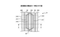
図3は、変調器21の構造の一例を示す図である。図4は、変調器21の構造の一例を示すX-X断面図である。図3のX-X断面が図4に対応する。変調器21は、信号配線220、グランド配線221、EOポリマー26、半導体層210、およびシリコン層211を備える。信号配線220、グランド配線221、EOポリマー26、半導体層210、およびシリコン層211は、導波路23に沿って配置されている。本実施例における変調器21は、EOポリマー26を用いた光変調器である。なお、図3では、図面の見やすさの観点から、EOポリマー26にハンチングが施されている。
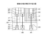
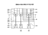
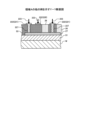
図2の領域Aを拡大すると、例えば図5のようになる。図5は、領域Aの一例を示す拡大図である。図6は、領域Aの一例を示すY-Y断面図である。図5のY-Y断面が図6に対応する。信号配線220の両脇には、2つのグランド配線221が配置されており、信号配線220と一方のグランド配線221との間には、EOポリマー26が配置されている。なお、図5では、図面の見やすさの観点から、EOポリマー26にハンチングが施されている。
次に、ステップ状の電気信号を供給した場合の伝送線路の特性インピーダンスZ0の変化をシミュレーションにより求めた。図9は、伝送線路の特性インピーダンスZ0の変化の一例を示す図である。図9には、パッド222にシリコン配線27が設けられていない場合の伝送線路の特性インピーダンスZ0の変化が比較例として示されている。
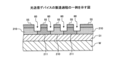
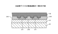
次に、光送信デバイス20の製造手順について図10~図16を参照しながら説明する。図10~図16は、光送信デバイス20の製造過程の一例を示す図である。図10~図16では、光送信デバイス20の中の変調器21の製造過程について例示されている。
上記説明から明らかなように、本実施例の光送信デバイス20は、基板Wと、導波路23と、信号配線220と、グランド配線221と、シリコン配線27とを備える。導波路23は、基板Wに設けられ、光信号を伝送する。信号配線220およびグランド配線221は、導波路23に沿って基板Wに配置され、端部に外部基板40とワイヤ223により電気接続されるパッド222を有する。シリコン配線27は、グランド配線221の端部に接続される。信号配線220とシリコン配線27との間の距離ΔL2は、信号配線220とグランド配線221との間の距離ΔL1よりも短い。これにより、信号の品質劣化を抑えることができる。
なお、開示の技術は、上記した各実施例に限定されるものではなく、その要旨の範囲内で数々の変形が可能である。
10 光送受信装置
11 光送受信部
12 LD
13 DSP
20 光送信デバイス
200 デバイス本体
21 変調器
210 半導体層
211 シリコン層
220 信号配線
221 グランド配線
222 パッド
223 ワイヤ
225 コンタクト
226 コンタクト
227 ビア
23 導波路
230 入力端
231 出力端
24 VOA
25 PR
26 EOポリマー
27 シリコン配線
28 mPD
29 PBC
30 光受信デバイス
40 外部基板
400 信号配線
401 グランド配線
402 パッド
41 終端基板
410 パッド
411 終端抵抗
51 BOX層
53 絶縁層
55 レジスト
60 凹部
61 凹部
62 凹部
Claims (10)
- 基板と、
前記基板に設けられ、光信号を伝送する導波路と、
前記基板に前記導波路に沿って配置され、端部に外部装置とワイヤにより電気接続されるボンディング部を有する信号配線およびグランド配線と、
前記グランド配線の下層に形成され、ビアを介して前記グランド配線の端部に接続された第1のスタブ配線と
を備え、
前記基板の面に交差する方向から見た場合に、前記信号配線と前記第1のスタブ配線とは離間しており、前記基板の面に交差する方向から見た場合の前記信号配線と前記グランド配線とが隣り合う方向における前記信号配線と前記第1のスタブ配線との間の距離は、前記基板の面に交差する方向から見た場合の前記信号配線と前記グランド配線とが隣り合う方向における前記信号配線と前記グランド配線との間の距離よりも短いことを特徴とする光デバイス。 - 前記基板には、複数の前記グランド配線が設けられており、
前記第1のスタブ配線は、ビアを介して複数の前記グランド配線に接続されていることを特徴とする請求項1に記載の光デバイス。 - 前記信号配線の端部に接続された第2のスタブ配線をさらに備え、
前記基板の面に交差する方向から見た場合に、前記信号配線と前記グランド配線とが隣り合う方向における前記第1のスタブ配線と前記第2のスタブ配線との間の距離は、前記信号配線と前記グランド配線とが隣り合う方向における前記信号配線と前記グランド配線との間の距離よりも短いことを特徴とする請求項1に記載の光デバイス。 - 前記信号配線および前記グランド配線に接続され、前記信号配線を介して供給される電気信号に応じて前記導波路を伝送される前記光信号を変調する光変調器を備えることを特徴とする請求項1から3のいずれか一項に記載の光デバイス。
- 前記光変調器は、EO(Electro Optic)ポリマーを用いた光変調器であり、
前記ボンディング部が形成された前記信号配線の端部と前記基板の端部との間、および、前記ボンディング部が形成された前記グランド配線の端部と前記基板の端部との間には、前記EOポリマーが配置されることを特徴とする請求項4に記載の光デバイス。 - 前記第1のスタブ配線は、シリコンにn型の不純物が添加されたシリコン配線であることを特徴とする請求項4または5に記載の光デバイス。
- 前記光変調器には、前記導波路に沿ってn型の不純物が添加されたシリコンである半導体層が設けられていることを特徴とする請求項6に記載の光デバイス。
- 前記第1のスタブ配線は、シリコンにp型の不純物が添加されたシリコン配線であることを特徴とする請求項4または5に記載の光デバイス。
- 前記光変調器には、前記導波路に沿ってp型の不純物が添加されたシリコンである半導体層が設けられていることを特徴とする請求項8に記載の光デバイス。
- 前記基板の面に交差する方向から見た場合に、前記グランド配線の延在方向における前記第1のスタブ配線と前記基板の端部との間の距離は、前記グランド配線の延在方向における前記グランド配線の端部と前記基板の端部との間の距離よりも短いことを特徴とする請求項1から9のいずれか一項に記載の光デバイス。
Priority Applications (3)
| Application Number | Priority Date | Filing Date | Title |
|---|---|---|---|
| JP2019139838A JP7404696B2 (ja) | 2019-07-30 | 2019-07-30 | 光デバイス |
| US16/907,723 US11294208B2 (en) | 2019-07-30 | 2020-06-22 | Optical device |
| CN202010602005.7A CN112305787B (zh) | 2019-07-30 | 2020-06-29 | 光器件 |
Applications Claiming Priority (1)
| Application Number | Priority Date | Filing Date | Title |
|---|---|---|---|
| JP2019139838A JP7404696B2 (ja) | 2019-07-30 | 2019-07-30 | 光デバイス |
Publications (2)
| Publication Number | Publication Date |
|---|---|
| JP2021021896A JP2021021896A (ja) | 2021-02-18 |
| JP7404696B2 true JP7404696B2 (ja) | 2023-12-26 |
Family
ID=74260311
Family Applications (1)
| Application Number | Title | Priority Date | Filing Date |
|---|---|---|---|
| JP2019139838A Active JP7404696B2 (ja) | 2019-07-30 | 2019-07-30 | 光デバイス |
Country Status (3)
| Country | Link |
|---|---|
| US (1) | US11294208B2 (ja) |
| JP (1) | JP7404696B2 (ja) |
| CN (1) | CN112305787B (ja) |
Families Citing this family (3)
| Publication number | Priority date | Publication date | Assignee | Title |
|---|---|---|---|---|
| JP7276001B2 (ja) * | 2019-08-27 | 2023-05-18 | 富士通オプティカルコンポーネンツ株式会社 | 光デバイス |
| US12126382B2 (en) * | 2022-05-31 | 2024-10-22 | Nokia Solutions And Networks Oy | Optimization of RF driver and/or optical device |
| USD1111491S1 (en) * | 2023-12-22 | 2026-02-10 | Apple Inc. | Bench |
Citations (7)
| Publication number | Priority date | Publication date | Assignee | Title |
|---|---|---|---|---|
| US20040066549A1 (en) | 2002-10-04 | 2004-04-08 | Jds Uniphase Corporation | Launch interface electrode structure for suppressing coupling to substrate modes for electro-optic modulator |
| US20060115197A1 (en) | 2004-11-30 | 2006-06-01 | Choi Kwang S | Optical module |
| JP2012078759A (ja) | 2010-10-06 | 2012-04-19 | Mitsubishi Electric Corp | 光変調器 |
| JP2016014697A (ja) | 2014-06-30 | 2016-01-28 | 株式会社フジクラ | 高周波回路及び光変調器 |
| JP2016051718A (ja) | 2014-08-28 | 2016-04-11 | 株式会社デンソー | 多層配線基板 |
| JP2016071241A (ja) | 2014-09-30 | 2016-05-09 | 住友大阪セメント株式会社 | 光デバイス |
| WO2017208526A1 (ja) | 2016-06-03 | 2017-12-07 | 三菱電機株式会社 | 光変調器 |
Family Cites Families (17)
| Publication number | Priority date | Publication date | Assignee | Title |
|---|---|---|---|---|
| US4340975A (en) * | 1979-10-09 | 1982-07-20 | Matsushita Electric Industrial Company, Limited | Microwave mixing circuit and a VHF-UHF tuner having the mixing circuit |
| US5606737A (en) * | 1992-03-09 | 1997-02-25 | Fujitsu Limited | Oscillator mixer and a multiplier mixer for outputting a baseband signal based upon an input and output signal |
| JPH1138372A (ja) * | 1997-07-24 | 1999-02-12 | Oki Electric Ind Co Ltd | 高周波回路、それを用いた光モジュール及びインピーダンス整合方法 |
| JP2001209017A (ja) | 1999-11-15 | 2001-08-03 | Mitsubishi Electric Corp | 光電変換半導体装置 |
| US7227246B2 (en) * | 2003-10-30 | 2007-06-05 | Avago Technologies Fiber Ip (Singapore) Pte. Ltd. | Matching circuits on optoelectronic devices |
| US7283689B1 (en) * | 2006-06-29 | 2007-10-16 | Intel Corporation | Optical waveguide having high dielectric constant contrast between cladding and core |
| US9172145B2 (en) * | 2006-09-21 | 2015-10-27 | Raytheon Company | Transmit/receive daughter card with integral circulator |
| US20090159326A1 (en) * | 2007-12-19 | 2009-06-25 | Richard Mellitz | S-turn via and method for reducing signal loss in double-sided printed wiring boards |
| WO2011056949A2 (en) | 2009-11-04 | 2011-05-12 | University Of Delaware | Eo polymer-based dual slot waveguide modulators |
| US8805130B2 (en) * | 2010-03-16 | 2014-08-12 | Cornell University | Semiconductor high-speed integrated electro-optic devices and methods |
| JP5477148B2 (ja) * | 2010-04-28 | 2014-04-23 | 日本電気株式会社 | 半導体光配線装置 |
| JP5360256B2 (ja) * | 2012-03-30 | 2013-12-04 | 住友大阪セメント株式会社 | 光導波路素子 |
| JP6425271B2 (ja) * | 2013-03-27 | 2018-11-21 | 日本電気株式会社 | 光受信回路 |
| US9766484B2 (en) * | 2014-01-24 | 2017-09-19 | Cisco Technology, Inc. | Electro-optical modulator using waveguides with overlapping ridges |
| JP2016018005A (ja) * | 2014-07-04 | 2016-02-01 | 株式会社フジクラ | 光導波路素子およびその製造方法、光受信回路、光変調器 |
| JP6229607B2 (ja) * | 2014-07-11 | 2017-11-15 | 富士通オプティカルコンポーネンツ株式会社 | 光モジュール及び送信装置 |
| JP6992961B2 (ja) * | 2017-03-31 | 2022-01-13 | 日本電気株式会社 | 電気光学変調器 |
-
2019
- 2019-07-30 JP JP2019139838A patent/JP7404696B2/ja active Active
-
2020
- 2020-06-22 US US16/907,723 patent/US11294208B2/en active Active
- 2020-06-29 CN CN202010602005.7A patent/CN112305787B/zh active Active
Patent Citations (7)
| Publication number | Priority date | Publication date | Assignee | Title |
|---|---|---|---|---|
| US20040066549A1 (en) | 2002-10-04 | 2004-04-08 | Jds Uniphase Corporation | Launch interface electrode structure for suppressing coupling to substrate modes for electro-optic modulator |
| US20060115197A1 (en) | 2004-11-30 | 2006-06-01 | Choi Kwang S | Optical module |
| JP2012078759A (ja) | 2010-10-06 | 2012-04-19 | Mitsubishi Electric Corp | 光変調器 |
| JP2016014697A (ja) | 2014-06-30 | 2016-01-28 | 株式会社フジクラ | 高周波回路及び光変調器 |
| JP2016051718A (ja) | 2014-08-28 | 2016-04-11 | 株式会社デンソー | 多層配線基板 |
| JP2016071241A (ja) | 2014-09-30 | 2016-05-09 | 住友大阪セメント株式会社 | 光デバイス |
| WO2017208526A1 (ja) | 2016-06-03 | 2017-12-07 | 三菱電機株式会社 | 光変調器 |
Non-Patent Citations (2)
| Title |
|---|
| F. Qiu et al.,Ultra-thin silicon/electro-optic polymer hybrid waveguide modulators,Applied Physics Letters,AIP Publishing,2015年09月21日,Vol. 107, No. 12,pp. 123302-1~123302-5,DOI:10.1063/1.4931490 |
| R. Palmer et al.,High-Speed, Low Drive-Voltage Silicon-Organic Hybrid Modulator Based on a Binary-Chromophore Electro-Optic Material,Journal of Lightwave Technology,IEEE,2014年08月15日,Vol. 32, No. 16,pp. 2726-2734,DOI: 10.1109/JLT.2014.2321498 |
Also Published As
| Publication number | Publication date |
|---|---|
| US20210033896A1 (en) | 2021-02-04 |
| CN112305787B (zh) | 2024-06-28 |
| CN112305787A (zh) | 2021-02-02 |
| US11294208B2 (en) | 2022-04-05 |
| JP2021021896A (ja) | 2021-02-18 |
Similar Documents
| Publication | Publication Date | Title |
|---|---|---|
| US9046703B2 (en) | Optical modulator module and semiconductor optical modulator | |
| US12164210B2 (en) | High frequency optical modulator with laterally displaced conduction plane relative to modulating electrodes | |
| JP7404696B2 (ja) | 光デバイス | |
| EP2905639B1 (en) | Shielding regions for photonic integrated circuits | |
| JP6432574B2 (ja) | 光変調器、及び光送信装置 | |
| US10921620B2 (en) | Optical modulator and optical transmission apparatus | |
| US10261252B2 (en) | Optical coupling device with a wide bandwidth and reduced power losses | |
| US20190187370A1 (en) | Semiconductor device | |
| CN113594188A (zh) | 针对集成器件的射频损失减少 | |
| JP7180538B2 (ja) | 光デバイス、試験方法、光送受信装置、および製造方法 | |
| JP2021026090A (ja) | 光デバイス | |
| JP7263972B2 (ja) | 光変調器及びそれを用いた光送信装置 | |
| JP7276001B2 (ja) | 光デバイス | |
| US12147097B2 (en) | Optical modulator and optical transmission apparatus using same | |
| JP3269654B2 (ja) | 光電子送受信装置 | |
| JP7388021B2 (ja) | 光デバイス | |
| CN114503359B (zh) | 高频封装 | |
| US20240379644A1 (en) | Optical Communication Device | |
| US9772461B2 (en) | Semiconductor integrated circuit and method for manufacturing the same |
Legal Events
| Date | Code | Title | Description |
|---|---|---|---|
| A621 | Written request for application examination |
Free format text: JAPANESE INTERMEDIATE CODE: A621 Effective date: 20220330 |
|
| A977 | Report on retrieval |
Free format text: JAPANESE INTERMEDIATE CODE: A971007 Effective date: 20221122 |
|
| A131 | Notification of reasons for refusal |
Free format text: JAPANESE INTERMEDIATE CODE: A131 Effective date: 20221129 |
|
| A131 | Notification of reasons for refusal |
Free format text: JAPANESE INTERMEDIATE CODE: A131 Effective date: 20230404 |
|
| A521 | Request for written amendment filed |
Free format text: JAPANESE INTERMEDIATE CODE: A523 Effective date: 20230601 |
|
| A131 | Notification of reasons for refusal |
Free format text: JAPANESE INTERMEDIATE CODE: A131 Effective date: 20230801 |
|
| A521 | Request for written amendment filed |
Free format text: JAPANESE INTERMEDIATE CODE: A523 Effective date: 20230928 |
|
| TRDD | Decision of grant or rejection written | ||
| A01 | Written decision to grant a patent or to grant a registration (utility model) |
Free format text: JAPANESE INTERMEDIATE CODE: A01 Effective date: 20231114 |
|
| A61 | First payment of annual fees (during grant procedure) |
Free format text: JAPANESE INTERMEDIATE CODE: A61 Effective date: 20231127 |
|
| R150 | Certificate of patent or registration of utility model |
Ref document number: 7404696 Country of ref document: JP Free format text: JAPANESE INTERMEDIATE CODE: R150 |