JP7404696B2 - optical device - Google Patents
optical device Download PDFInfo
- Publication number
- JP7404696B2 JP7404696B2 JP2019139838A JP2019139838A JP7404696B2 JP 7404696 B2 JP7404696 B2 JP 7404696B2 JP 2019139838 A JP2019139838 A JP 2019139838A JP 2019139838 A JP2019139838 A JP 2019139838A JP 7404696 B2 JP7404696 B2 JP 7404696B2
- Authority
- JP
- Japan
- Prior art keywords
- wiring
- signal
- ground
- optical
- silicon
- Prior art date
- Legal status (The legal status is an assumption and is not a legal conclusion. Google has not performed a legal analysis and makes no representation as to the accuracy of the status listed.)
- Active
Links
Images


Classifications
-
- G—PHYSICS
- G02—OPTICS
- G02F—OPTICAL DEVICES OR ARRANGEMENTS FOR THE CONTROL OF LIGHT BY MODIFICATION OF THE OPTICAL PROPERTIES OF THE MEDIA OF THE ELEMENTS INVOLVED THEREIN; NON-LINEAR OPTICS; FREQUENCY-CHANGING OF LIGHT; OPTICAL LOGIC ELEMENTS; OPTICAL ANALOGUE/DIGITAL CONVERTERS
- G02F1/00—Devices or arrangements for the control of the intensity, colour, phase, polarisation or direction of light arriving from an independent light source, e.g. switching, gating or modulating; Non-linear optics
- G02F1/01—Devices or arrangements for the control of the intensity, colour, phase, polarisation or direction of light arriving from an independent light source, e.g. switching, gating or modulating; Non-linear optics for the control of the intensity, phase, polarisation or colour
- G02F1/015—Devices or arrangements for the control of the intensity, colour, phase, polarisation or direction of light arriving from an independent light source, e.g. switching, gating or modulating; Non-linear optics for the control of the intensity, phase, polarisation or colour based on semiconductor elements having potential barriers, e.g. having a PN or PIN junction
- G02F1/025—Devices or arrangements for the control of the intensity, colour, phase, polarisation or direction of light arriving from an independent light source, e.g. switching, gating or modulating; Non-linear optics for the control of the intensity, phase, polarisation or colour based on semiconductor elements having potential barriers, e.g. having a PN or PIN junction in an optical waveguide structure
-
- G—PHYSICS
- G02—OPTICS
- G02F—OPTICAL DEVICES OR ARRANGEMENTS FOR THE CONTROL OF LIGHT BY MODIFICATION OF THE OPTICAL PROPERTIES OF THE MEDIA OF THE ELEMENTS INVOLVED THEREIN; NON-LINEAR OPTICS; FREQUENCY-CHANGING OF LIGHT; OPTICAL LOGIC ELEMENTS; OPTICAL ANALOGUE/DIGITAL CONVERTERS
- G02F1/00—Devices or arrangements for the control of the intensity, colour, phase, polarisation or direction of light arriving from an independent light source, e.g. switching, gating or modulating; Non-linear optics
- G02F1/01—Devices or arrangements for the control of the intensity, colour, phase, polarisation or direction of light arriving from an independent light source, e.g. switching, gating or modulating; Non-linear optics for the control of the intensity, phase, polarisation or colour
- G02F1/061—Devices or arrangements for the control of the intensity, colour, phase, polarisation or direction of light arriving from an independent light source, e.g. switching, gating or modulating; Non-linear optics for the control of the intensity, phase, polarisation or colour based on electro-optical organic material
- G02F1/065—Devices or arrangements for the control of the intensity, colour, phase, polarisation or direction of light arriving from an independent light source, e.g. switching, gating or modulating; Non-linear optics for the control of the intensity, phase, polarisation or colour based on electro-optical organic material in an optical waveguide structure
-
- H—ELECTRICITY
- H04—ELECTRIC COMMUNICATION TECHNIQUE
- H04B—TRANSMISSION
- H04B10/00—Transmission systems employing electromagnetic waves other than radio-waves, e.g. infrared, visible or ultraviolet light, or employing corpuscular radiation, e.g. quantum communication
- H04B10/50—Transmitters
- H04B10/516—Details of coding or modulation
-
- G—PHYSICS
- G02—OPTICS
- G02F—OPTICAL DEVICES OR ARRANGEMENTS FOR THE CONTROL OF LIGHT BY MODIFICATION OF THE OPTICAL PROPERTIES OF THE MEDIA OF THE ELEMENTS INVOLVED THEREIN; NON-LINEAR OPTICS; FREQUENCY-CHANGING OF LIGHT; OPTICAL LOGIC ELEMENTS; OPTICAL ANALOGUE/DIGITAL CONVERTERS
- G02F2202/00—Materials and properties
- G02F2202/02—Materials and properties organic material
- G02F2202/022—Materials and properties organic material polymeric
Landscapes
- Physics & Mathematics (AREA)
- Nonlinear Science (AREA)
- General Physics & Mathematics (AREA)
- Optics & Photonics (AREA)
- Electromagnetism (AREA)
- Engineering & Computer Science (AREA)
- Computer Networks & Wireless Communication (AREA)
- Signal Processing (AREA)
- Optical Modulation, Optical Deflection, Nonlinear Optics, Optical Demodulation, Optical Logic Elements (AREA)
Description
本発明は、光デバイスに関する。 TECHNICAL FIELD The present invention relates to optical devices.
光変調器等の光デバイスの小型化が進んでいる。シリコン導波路は光の閉じ込め効果が強く、導波路の曲げ半径を小さくできるので、従来のLN変調器や化合物半導体変調器に比べて光変調器のサイズを小さくすることができる。シリコン導波路を用いた光変調器では、シリコン導波路にPN接合部を設け、メタル配線を介してPN接合部に電圧を印加することにより、PN接合部に電界を発生させ、シリコン導波路の屈折率を変化させる。シリコン導波路の屈折率が変化すると、シリコン導波路を伝搬する光信号の速度が変化し、シリコン導波路から出力される光信号の位相が変化する。シリコン導波路を用いた光変調器では、この性質を利用して光信号を変調することができる。 Optical devices such as optical modulators are becoming smaller. Silicon waveguides have a strong light confinement effect, and the bending radius of the waveguide can be made small, so the size of the optical modulator can be made smaller than conventional LN modulators or compound semiconductor modulators. In an optical modulator using a silicon waveguide, a PN junction is provided in the silicon waveguide, and by applying a voltage to the PN junction via metal wiring, an electric field is generated at the PN junction, and the PN junction is Changes the refractive index. When the refractive index of the silicon waveguide changes, the speed of the optical signal propagating through the silicon waveguide changes, and the phase of the optical signal output from the silicon waveguide changes. An optical modulator using a silicon waveguide can utilize this property to modulate an optical signal.
光変調器等の光デバイスには、電気信号を入力するためドライバ回路等の他の外部装置が、例えば金属ワイヤ等によって接続される。金属ワイヤは、光変調器等の光デバイスの信号配線やグランド配線に設けられたパッドと、ドライバ回路等の外部装置の信号配線やグランド配線に設けられたパッドとを接続する。 Other external devices such as driver circuits are connected to optical devices such as optical modulators by, for example, metal wires in order to input electrical signals. The metal wire connects pads provided on signal wiring and ground wiring of an optical device such as an optical modulator and pads provided on signal wiring and ground wiring of an external device such as a driver circuit.
ところで、光デバイスの小型化が進むと、複数の光デバイスをシリコン等の基板上に複数形成することが可能になる。基板上に形成された複数の光デバイスは、ダイシングにより個々のデバイスに分離される。近年、デバイスへのダメージが低いこと、ダイシングにより発生するダストが少ないこと等の利点から、レーザ光を用いたダイシング技術が用いられている。レーザ光を用いたダイシングでは、レーザ光が透過しない金属をダイシングすることが難しいため、金属配線等は、ダイシングラインから所定距離以上離れた領域に配置される。例えば、金属ワイヤがボンディングされるパッドは、光デバイスの端部から所定距離以上離れた位置に配置されることになる。 By the way, as optical devices become smaller, it becomes possible to form a plurality of optical devices on a substrate such as silicon. A plurality of optical devices formed on a substrate are separated into individual devices by dicing. In recent years, dicing technology using laser light has been used because of its advantages such as low damage to devices and little dust generated by dicing. In dicing using laser light, it is difficult to dice metal through which the laser light does not pass, so metal wiring and the like are placed in an area separated by a predetermined distance or more from the dicing line. For example, a pad to which a metal wire is bonded will be placed at a position a predetermined distance or more away from the end of the optical device.
パッドと光デバイスの端部との距離が離れていると、ドライバ回路等の外部装置のパッドとの距離が長くなり、パッドどうしを接続する金属ワイヤも長くなる。金属ワイヤが長くなると、配線の特性インピーダンスが大きくなり、インピーダンスの不整合による電気信号の反射が生じる。電気信号の反射が生じると、信号帯域の中で、反射波に応じた一部の周波数の信号の強度が変動し、信号の品質が劣化する。 If the distance between the pad and the end of the optical device is large, the distance from the pad of an external device such as a driver circuit will be long, and the metal wire connecting the pads will also be long. As the metal wire becomes longer, the characteristic impedance of the wiring increases, causing reflection of electrical signals due to impedance mismatch. When an electric signal is reflected, the strength of the signal at a certain frequency in the signal band varies depending on the reflected wave, and the quality of the signal deteriorates.
本願に開示の技術は、上記に鑑みてなされたものであって、信号の品質劣化を抑えることができる光デバイスを提供することを目的とする。 The technology disclosed in this application has been made in view of the above, and aims to provide an optical device that can suppress signal quality deterioration.
1つの側面では、光デバイスは、基板と、導波路と、信号配線と、グランド配線と、第1のスタブ配線とを備える。導波路は、基板に設けられ、光信号を伝送する。信号配線およびグランド配線は、導波路に沿って基板に配置され、端部に外部装置とワイヤにより電気接続されるボンディング部を有する。第1のスタブ配線は、グランド配線の端部に接続される。信号配線と第1のスタブ配線との間の距離は、信号配線とグランド配線との間の距離よりも短い。 In one aspect, an optical device includes a substrate, a waveguide, a signal wiring, a ground wiring, and a first stub wiring. The waveguide is provided on the substrate and transmits optical signals. The signal wiring and the ground wiring are arranged on the substrate along the waveguide, and have a bonding part at an end that is electrically connected to an external device by a wire. The first stub wiring is connected to the end of the ground wiring. The distance between the signal wiring and the first stub wiring is shorter than the distance between the signal wiring and the ground wiring.
1実施形態によれば、信号の品質劣化を抑えることができる。 According to one embodiment, signal quality deterioration can be suppressed.
以下に、本願が開示する光デバイスの実施例を、図面に基づいて詳細に説明する。なお、以下に示す実施例は、開示の技術を限定するものではない。 Examples of the optical device disclosed in the present application will be described in detail below based on the drawings. Note that the examples shown below do not limit the disclosed technology.
[光送受信装置10の構成]
図1は、光送受信装置10の一例を示す図である。本実施例における光送受信装置10は、光送受信部11、LD(Laser Diode)12、およびDSP(Digital Signal Processor)13を備える。光送受信部11は、光送信デバイス20および光受信デバイス30を有する。光送信デバイス20および光受信デバイス30は、光デバイスの一例である。
[Configuration of optical transmitter/receiver 10]
FIG. 1 is a diagram showing an example of an optical transmitter/
光送信デバイス20は、LD12から供給された光を、DSP13から出力された送信信号に基づいて変調する。そして、光送信デバイス20は、送信信号に応じて変調された光信号(Tx_out)を出力する。光受信デバイス30は、光信号(Rx_in)を受光する。受光された光信号は、偏波分離され、LD12から供給された光を用いて復調され、電気信号に変換されてDSP13へ出力される。
The
[光送信デバイス20の構成]
図2は、光送信デバイス20の一例を示す図である。光送信デバイス20は、デバイス本体200を備える。デバイス本体200には、ワイヤ223を介して外部基板40および終端基板41が接続される。外部基板40には、デバイス本体200に送信信号に基づく電気信号を供給するドライバ回路等が実装されている。終端基板41には、デバイス本体200に設けられた配線に接続される終端抵抗が実装されている。
[Configuration of optical transmission device 20]
FIG. 2 is a diagram showing an example of the
デバイス本体200は、XI変調器21-1、XQ変調器21-2、YI変調器21-3、およびYQ変調器21-4を有する。また、光送信デバイス20は、VOA24-1、VOA24-2、PR25、EO(Electro Optic)ポリマー26、mPD28-1、mPD28-2、およびPBC29を有する。VOAはVariable Optical Attenuatorの略であり、PRはPolarization Rotatorの略であり、mPDはmonitor PhotoDiodeの略であり、PBCはPolarization Beam Combinerの略である。
The
なお、以下では、XI変調器21-1、XQ変調器21-2、YI変調器21-3、およびYQ変調器21-4のそれぞれを区別することなく総称する場合に変調器21と記載する。また、以下では、VOA24-1およびVOA24-2のそれぞれを区別することなく総称する場合にVOA24と記載し、mPD28-1およびmPD28-2のそれぞれを区別することなく総称する場合にmPD28と記載する。また、図2では、図面の見やすさの観点から、EOポリマー26にハンチングが施されている。
Note that, hereinafter, when the XI modulator 21-1, the XQ modulator 21-2, the YI modulator 21-3, and the YQ modulator 21-4 are collectively referred to without distinction, they will be referred to as the
デバイス本体200上には、光信号を伝搬する導波路23が形成されている。LD12から出力された光は、導波路23の入力端230から入力され、導波路23を介してそれぞれの変調器21に入力される。それぞれの変調器21には、電気信号である送信信号を伝送する信号配線220と、グランドに接続されるグランド配線221と、信号配線220およびグランド配線221の間に配置されたEOポリマー26とが、導波路23に沿って配置されている。それぞれの変調器21では、信号配線220とグランド配線221との間に印加される電圧に応じて信号配線220とグランド配線221の間に配置されたEOポリマー26の屈折率が変化する。これにより、EOポリマー26に沿って配置された導波路23内を伝搬する光の位相が変化する。信号配線220に印加される電圧を送信信号に応じて変化させることにより、送信信号に応じて光を変調することができる。それぞれの変調器21において、送信信号は、光信号の入力端側の信号配線220に供給される。
A
それぞれの変調器21によって変調された光信号は、VOA24によって強度が調整される。VOA24から出力された光信号は、mPD28によって受光される。VOA24は、mPD28の受光電流に応じて、光信号の強度を調整する。 The intensity of the optical signal modulated by each modulator 21 is adjusted by the VOA 24. The optical signal output from the VOA 24 is received by the mPD 28. The VOA 24 adjusts the intensity of the optical signal according to the light reception current of the mPD 28.
PR25は、VOA24-2によって強度が調整された光信号の偏光面を回転させる。VOA24-1によって強度が調整された光信号は、PBC29によって偏光面が回転された光信号と合成され、光信号(Tx_out)として導波路23の出力端231から出力される。
The
信号配線220およびグランド配線221の両端には、ワイヤ223がボンディングされるパッド222が設けられている。パッド222は、ボンディング部の一例である。それぞれのパッド222には、シリコン配線27が接続されている。パッド222は、デバイス本体200の表面に配置されており、シリコン配線27は、デバイス本体200の内部に配置されている。パッド222とシリコン配線27とは、それぞれビアを介して接続されている。また、パッド222が形成された信号配線220の端部とデバイス本体200の端部との間、および、パッド222が形成されたグランド配線221の端部とデバイス本体200の端部との間には、EOポリマー26が配置されている。
本実施例において、シリコン配線27は、例えばリン等のn型の不純物が高濃度に添加されたシリコンである。なお、シリコン配線27は、例えばボロン等のp型の不純物が高濃度に添加されたシリコンであってもよい。グランド配線221のパッド222に接続されたシリコン配線27は、第1のスタブ配線の一例であり、信号配線220のパッド222に接続されたシリコン配線27は、第2のスタブ配線の一例である。
In this embodiment, the
外部基板40には、送信信号が伝送される信号配線400と、グランドに接続されるグランド配線401とが設けられている。信号配線400およびグランド配線401の端部には、ワイヤ223がボンディングされるパッド402が設けられている。終端基板41には、ワイヤ223がボンディングされるパッド410が設けられている。ワイヤ223を介して信号配線220に接続されるパッド410と、ワイヤ223を介してグランド配線221に接続されるパッド410との間には、終端抵抗411(例えば50Ω)が接続されている。
The
[変調器21の構造]
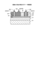
図3は、変調器21の構造の一例を示す図である。図4は、変調器21の構造の一例を示すX-X断面図である。図3のX-X断面が図4に対応する。変調器21は、信号配線220、グランド配線221、EOポリマー26、半導体層210、およびシリコン層211を備える。信号配線220、グランド配線221、EOポリマー26、半導体層210、およびシリコン層211は、導波路23に沿って配置されている。本実施例における変調器21は、EOポリマー26を用いた光変調器である。なお、図3では、図面の見やすさの観点から、EOポリマー26にハンチングが施されている。
[Structure of modulator 21]
FIG. 3 is a diagram showing an example of the structure of the
例えば図4に示されるように、半導体層210およびシリコン層211は、単結晶シリコン等の基板W上に積層されたBOX(Buried OXide)層51上に形成されている。半導体層210およびシリコン層211の上には、酸化シリコン等の絶縁層53が積層されており、信号配線220およびグランド配線221は、絶縁層53上に形成されている。
For example, as shown in FIG. 4, a
本実施例において、半導体層210は、例えばリン等のn型の不純物が高濃度に添加されたシリコンである。なお、半導体層210は、例えばボロン等のp型の不純物が低濃度に添加されたシリコンであってもよい。シリコン層211は、例えばシリコンで形成されており、導波路23として機能する。
In this embodiment, the
導波路23に沿ってシリコン層211の両脇に配置された一方の半導体層210には、金属を含む材料で構成されたコンタクト225を介して信号配線220が接続されている。また、他方の半導体層210には、金属を含む材料で構成されたコンタクト226を介してグランド配線221が接続されている。絶縁層53とシリコン層211とで囲まれた凹部には、EOポリマー26が配置されている。
A
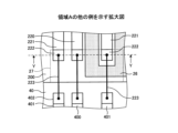
[パッド222付近の構造]
図2の領域Aを拡大すると、例えば図5のようになる。図5は、領域Aの一例を示す拡大図である。図6は、領域Aの一例を示すY-Y断面図である。図5のY-Y断面が図6に対応する。信号配線220の両脇には、2つのグランド配線221が配置されており、信号配線220と一方のグランド配線221との間には、EOポリマー26が配置されている。なお、図5では、図面の見やすさの観点から、EOポリマー26にハンチングが施されている。
[Structure near pad 222]
When area A in FIG. 2 is enlarged, it becomes, for example, as shown in FIG. 5. FIG. 5 is an enlarged view showing an example of area A. FIG. 6 is a YY cross-sectional view showing an example of area A. The YY cross section in FIG. 5 corresponds to FIG. 6. Two
ここで、信号配線220、グランド配線221、およびEOポリマー26は、製造の容易性等の観点からデバイス本体200の表面に配置されることが多い。信号配線220、グランド配線221、およびEOポリマー26がデバイス本体200の表面に配置される場合、信号配線220およびグランド配線221と、EOポリマー26とが交差しないように配置することになる。そのため、例えば図2および図5に示されるように、信号配線220およびグランド配線221と、デバイス本体200の端部との間にEOポリマー26が配置され、パッド222とデバイス本体200の端部との距離が長くなる。これにより、デバイス本体200のパッド222と外部基板40のパッド402とを接続するワイヤが長くなってしまう。ワイヤが長くなると、伝送線路の誘導成分が増加し、伝送線路の特性インピーダンスが増加する。伝送線路の特性インピーダンスが増加すると、特性インピーダンスの不整合による電気信号の反射が生じる。電気信号の反射が生じると、信号帯域の中で、反射波に応じた一部の周波数の信号の強度が変動し、信号の品質が劣化する。
Here, the
そこで、本実施例では、信号配線220およびグランド配線221のそれぞれに、パッド222に接続されたシリコン配線27が設けられる。シリコン配線27は、例えば図6に示されるように、金属を含む材料で構成されたビア227を介してパッド222に接続されている。
Therefore, in this embodiment, a
また、本実施例では、グランド配線221のパッド222に接続されたシリコン配線27と信号配線220との間の距離ΔL2は、例えば図5および図6に示されるように、信号配線220とグランド配線221との間の距離ΔL1よりも短い。これにより、パッド222付近の伝送線路において、信号配線220とグランド配線221との間の容量成分が増加し、パッド222付近の伝送線路の特性インピーダンスを減少させることができる。これにより、パッド222付近の伝送線路の特性インピーダンスの増加を抑制することができ、特性インピーダンスの不整合を抑制することができる。これにより、電気信号の反射を低減することができ、電気信号の品質劣化を抑制することができる。
Further, in this embodiment, the distance ΔL2 between the
なお、図5および図6の例では、信号配線220のパッド222に接続されたシリコン配線27とグランド配線221のパッド222に接続されたシリコン配線27との間の距離ΔL3は、信号配線220とグランド配線221との間の距離ΔL1よりもさらに短い。これにより、パッド222付近の伝送線路の特性インピーダンスの増加をさらに抑制することができ、電気信号の反射をさらに低減することができる。
In the examples of FIGS. 5 and 6, the distance ΔL3 between the
また、図2の領域Bを拡大すると、例えば図7のようになる。図7は、領域Bの一例を示す拡大図である。図8は、領域Bの一例を示すZ-Z断面図である。図7のZ-Z断面が図8に対応する。なお、図7では、図面の見やすさの観点から、EOポリマー26にハンチングが施されている。
Furthermore, when region B in FIG. 2 is enlarged, it becomes as shown in FIG. 7, for example. FIG. 7 is an enlarged view showing an example of area B. FIG. 8 is a ZZ cross-sectional view showing an example of region B. The ZZ cross section in FIG. 7 corresponds to FIG. 8. Note that in FIG. 7, hunting is applied to the
終端基板41と接続されるパッド222においても、例えば図7および図8に示されるように、シリコン配線27が設けられている。図7および図8においても、グランド配線221のパッド222に接続されたシリコン配線27と信号配線220との間の距離ΔL2は、信号配線220とグランド配線221との間の距離ΔL1よりも短くなっている。さらに、図7および図8においても、信号配線220のパッド222に接続されたシリコン配線27とグランド配線221のパッド222に接続されたシリコン配線27との間の距離ΔL3は、距離ΔL1よりもさらに短くなっている。これにより、終端基板41と接続されるパッド222においても、電気信号の反射を低減することができ、電気信号の品質劣化を抑制することができる。
Also in the
[シミュレーション結果]
次に、ステップ状の電気信号を供給した場合の伝送線路の特性インピーダンスZ0の変化をシミュレーションにより求めた。図9は、伝送線路の特性インピーダンスZ0の変化の一例を示す図である。図9には、パッド222にシリコン配線27が設けられていない場合の伝送線路の特性インピーダンスZ0の変化が比較例として示されている。
[simulation result]
Next, the change in the characteristic impedance Z 0 of the transmission line when a step-like electric signal was supplied was determined by simulation. FIG. 9 is a diagram showing an example of a change in the characteristic impedance Z 0 of the transmission line. FIG. 9 shows, as a comparative example, a change in the characteristic impedance Z 0 of the transmission line when the
図9から明らかなように、パッド222にシリコン配線27が設けられている本実施例の構成では、パッド222にシリコン配線27が設けられていない比較例の構成に比べて、伝送線路の特性インピーダンスZ0増加が抑えられている。従って、本実施例は、比較例に比べて、伝送線路の特性インピーダンスZ0の不整合を抑制でき、電気信号の品質劣化を抑制することができる。
As is clear from FIG. 9, in the configuration of this example in which the
[光送信デバイス20の製造手順]
次に、光送信デバイス20の製造手順について図10~図16を参照しながら説明する。図10~図16は、光送信デバイス20の製造過程の一例を示す図である。図10~図16では、光送信デバイス20の中の変調器21の製造過程について例示されている。
[Procedure for manufacturing optical transmitting device 20]
Next, the manufacturing procedure of the
まず、例えば図10に示されるように、基板W上にBOX層51が積層され、BOX層51上にシリコン層211が積層される。そして、シリコン層211上にレジスト55が積層され、半導体層210が配置される領域が露出するように、レジスト55がパターニングされる。そして、例えば図11に示されるように、レジスト55で覆われていないシリコン層211の領域に、例えばリン等のn型の不純物のイオンが注入される。これにより、n型の不純物が高濃度に添加された半導体層210が形成される。そして、レジスト55が除去される。
First, as shown in FIG. 10, for example, a
なお、図11に例示された工程では、シリコン配線27が形成される領域も露出するように、レジスト55がパターニングされる。これにより、シリコン配線27が形成されるシリコン層211の領域にもn型の不純物のイオンが注入され、n型の不純物が高濃度に添加されたシリコン配線27が形成される。
Note that in the step illustrated in FIG. 11, the resist 55 is patterned so that the region where the
次に、再びシリコン層211上にレジスト55が積層され、導波路23となるシリコン層211の部分の両脇の領域が露出するように、レジスト55がパターニングされる。そして、例えば図12に示されるように、レジスト55で覆われていない半導体層210およびシリコン層211の領域がエッチングされる。これにより、例えば図12に示されるように、導波路23となるシリコン層211の部分に沿って凹部60が形成される。そして、レジスト55が除去される。
Next, a resist 55 is laminated on the
次に、例えば図13に示されるように、半導体層210およびシリコン層211を覆うように絶縁層53が積層される。そして、絶縁層53上にレジスト55が積層され、コンタクト225およびコンタクト226が形成される領域が露出するように、レジスト55がパターニングされる。そして、レジスト55で覆われていない領域がエッチングされることにより、例えば図14に示されるように、絶縁層53に凹部61が形成される。そして、レジスト55が除去される。
Next, as shown in FIG. 13, for example, an insulating
この時、パッド222のビア227が形成される領域も露出するように、レジスト55がパターニングされ、レジスト55で覆われていない領域がエッチングされる。これにより、ビア227が形成される位置の絶縁層53にも凹部61が形成される。
At this time, the resist 55 is patterned so that the region of the
次に、凹部61内に金属を含む配線材料が埋め込まれ、配線材料がパターニングされる。これにより、例えば図15に示されるように、信号配線220、グランド配線221、コンタクト225、およびコンタクト226が形成される。
Next, a wiring material containing metal is embedded in the
この時、ビア227の位置に形成された凹部61内にも金属を含む配線材料が埋め込まれ、配線材料がパターニングされる。これにより、例えば図6および図8に示されたように、パッド222およびビア227が形成される。
At this time, the wiring material containing metal is also embedded in the
次に、再びレジスト55が積層され、EOポリマー26が配置される領域が露出するようにレジスト55がパターニングされる。そして、レジスト55で覆われていない領域がエッチングされることにより、例えば図16に示されるように、EOポリマー26が配置される領域に対応する凹部62が形成される。そして、レジスト55が除去され、凹部62内にEOポリマー26が配置される。これにより、例えば図4に示した変調器21が形成される。
Next, the resist 55 is laminated again, and the resist 55 is patterned so that the region where the
[実施例の効果]
上記説明から明らかなように、本実施例の光送信デバイス20は、基板Wと、導波路23と、信号配線220と、グランド配線221と、シリコン配線27とを備える。導波路23は、基板Wに設けられ、光信号を伝送する。信号配線220およびグランド配線221は、導波路23に沿って基板Wに配置され、端部に外部基板40とワイヤ223により電気接続されるパッド222を有する。シリコン配線27は、グランド配線221の端部に接続される。信号配線220とシリコン配線27との間の距離ΔL2は、信号配線220とグランド配線221との間の距離ΔL1よりも短い。これにより、信号の品質劣化を抑えることができる。
[Effects of Examples]
As is clear from the above description, the
また、上記した実施例の光送信デバイス20は、信号配線220の端部に接続されたシリコン配線27をさらに備える。グランド配線221に接続されたシリコン配線27と信号配線220に接続されたシリコン配線27との間の距離ΔL3は、信号配線220とグランド配線221との間の距離ΔL1よりも短い。これにより、信号の品質劣化をさらに抑えることができる。
Further, the
また、上記した実施例の光送信デバイス20は、変調器21を備える。変調器21は、信号配線220およびグランド配線221に接続され、信号配線220を介して供給される電気信号に応じて導波路23を伝送される光信号を変調する。これにより、変調器21において、信号の品質劣化を抑えることができる。
Further, the
また、上記した実施例における変調器21は、EOポリマー26を用いた光変調器である。パッド222が形成された信号配線220の端部と基板Wの端部との間、および、パッド222が形成されたグランド配線221の端部と基板Wの端部との間には、EOポリマー26が配置されている。これにより、EOポリマー26を用いた変調器21においても、信号の品質劣化を抑えることができる。
Further, the
また、上記した実施例において、シリコン配線27には、n型の不純物が添加されている。これにより、シリコン配線27の抵抗値を小さくすることができる。なお、上記した実施例において、シリコン配線27には、n型の不純物に代えてp型の不純物が添加されていてもよい。
Further, in the above embodiment, the
また、上記した実施例において、変調器21には、導波路23に沿ってn型の不純物が添加されたシリコンである半導体層210が設けられている。これにより、変調器21を製造するプロセスの中で、併せてシリコン配線27を形成することができるため、基板W上にシリコン配線27を効率よく形成することができる。なお、変調器21の半導体層210は、p型の不純物が添加されたシリコンであってもよい。
Furthermore, in the above-described embodiment, the
<その他>
なお、開示の技術は、上記した各実施例に限定されるものではなく、その要旨の範囲内で数々の変形が可能である。
<Others>
Note that the disclosed technology is not limited to the embodiments described above, and can be modified in many ways within the scope of its gist.
例えば、上記した実施例では、信号配線220およびグランド配線221の端部と、信号配線220およびグランド配線221の端部に設けられたシリコン配線27とは、基板Wの端部から所定距離以上離れた位置に配置されている。しかし、シリコン配線27が配置される位置は、これに限られない。シリコン配線27と基板Wの端部との間の距離は、信号配線220およびグランド配線221の端部と基板Wの端部との間の距離よりも短くてもよい。例えば図17に示されるように、シリコン配線27は、基板Wの端部まで延在していてもよい。図17は、領域Aの他の例を示す拡大図である。なお、領域Bも同様の構成とされてもよい。
For example, in the embodiment described above, the ends of the
これにより、パッド222付近の容量成分をより増加させることができるため、パッド222付近の伝送線路の特性インピーダンスの増加をより抑制することができる。これにより、特性インピーダンスの不整合をより抑制することができ、電気信号の反射をより低減することができる。
Thereby, the capacitance component near the
なお、デバイス本体200は、基板W上に複数形成され、例えばレーザ光を用いたダイシングにより個々のデバイス本体200に分離される。そのため、レーザ光が透過しない金属配線とダイシングラインとが交差すると、レーザ光を用いて基板Wをダイシングすることが難しい。そのため、信号配線220およびグランド配線221は、ダイシングラインから所定距離以上離れた位置に配置される。一方、シリコン配線27は、レーザ光を透過するシリコンにより形成される。そのため、シリコン配線27とダイシングラインとが交差しても、レーザ光によってダイシングすることができる。そのため、シリコン配線27と基板Wの端部との間の距離を、信号配線220およびグランド配線221と基板Wの端部との間の距離よりも短くすることができる。
Note that a plurality of
また、図17に例示された構成において、信号配線220の端部に接続されたシリコン配線27によって信号の反射が生じる場合には、例えば図18に示されるように、信号配線220にはシリコン配線27が設けられなくてもよい。図18は、領域Aの他の例を示す拡大図である。なお、領域Bも同様の構成とされてもよい。
In addition, in the configuration illustrated in FIG. 17, if signal reflection occurs due to the
また、例えば図19に示されるように、1つのシリコン配線27によって複数のグランド配線221のパッド222が接続されてもよい。図19は、領域Aの他の例を示す拡大図である。なお、領域Bも同様の構成とされてもよい。これにより、パッド222付近の容量成分をより増加させることができるため、電気信号の反射をより低減することができる。
Further, as shown in FIG. 19, for example,
また、複数のグランド配線221のパッド222に接続されるシリコン配線27は、例えば図20および図21に示されるように、信号配線220の下層に配置されてもよい。図20は、領域Aの他の例を示す拡大図であり、図21は、領域Aの他の例を示すY-Y断面図である。なお、領域Bも同様の構成とされてもよい。
Further, the
また、上記した実施例では、EOポリマーを用いた変調器21を備える光送信デバイス20を例に説明したが、開示の技術はこれに限られない。例えばシリコン導波路に設けられたPN接合部に電圧を印加することにより、シリコン導波路を伝送される光信号の位相を変える光変調器を備える光送信デバイス20においても、開示の技術を適用することができる。
Further, in the above-described embodiments, the
また、上記した実施例では、光デバイスとして光送信デバイス20を例に説明したが、開示の技術はこれに限られない。例えば光受信デバイス30においても、上記した実施例に開示された技術を適用することができる。
Furthermore, in the embodiments described above, the
W 基板
10 光送受信装置
11 光送受信部
12 LD
13 DSP
20 光送信デバイス
200 デバイス本体
21 変調器
210 半導体層
211 シリコン層
220 信号配線
221 グランド配線
222 パッド
223 ワイヤ
225 コンタクト
226 コンタクト
227 ビア
23 導波路
230 入力端
231 出力端
24 VOA
25 PR
26 EOポリマー
27 シリコン配線
28 mPD
29 PBC
30 光受信デバイス
40 外部基板
400 信号配線
401 グランド配線
402 パッド
41 終端基板
410 パッド
411 終端抵抗
51 BOX層
53 絶縁層
55 レジスト
60 凹部
61 凹部
62 凹部
13 DSP
20
25 PR
26
29 PBC
30
Claims (10)
前記基板に設けられ、光信号を伝送する導波路と、
前記基板に前記導波路に沿って配置され、端部に外部装置とワイヤにより電気接続されるボンディング部を有する信号配線およびグランド配線と、
前記グランド配線の下層に形成され、ビアを介して前記グランド配線の端部に接続された第1のスタブ配線と
を備え、
前記基板の面に交差する方向から見た場合に、前記信号配線と前記第1のスタブ配線とは離間しており、前記基板の面に交差する方向から見た場合の前記信号配線と前記グランド配線とが隣り合う方向における前記信号配線と前記第1のスタブ配線との間の距離は、前記基板の面に交差する方向から見た場合の前記信号配線と前記グランド配線とが隣り合う方向における前記信号配線と前記グランド配線との間の距離よりも短いことを特徴とする光デバイス。 A substrate and
a waveguide provided on the substrate and transmitting an optical signal;
signal wiring and ground wiring arranged on the substrate along the waveguide and having a bonding part electrically connected to an external device by a wire at an end;
a first stub wiring formed in a layer below the ground wiring and connected to an end of the ground wiring via a via ;
The signal wiring and the first stub wiring are separated from each other when viewed from the direction crossing the surface of the substrate, and the signal wiring and the ground when viewed from the direction crossing the surface of the substrate The distance between the signal wiring and the first stub wiring in the direction in which the wirings are adjacent to each other is the distance between the signal wiring and the first stub wiring in the direction in which the signal wiring and the ground wiring are adjacent to each other when viewed from a direction intersecting the surface of the substrate. An optical device characterized in that the distance is shorter than the distance between the signal wiring and the ground wiring.
前記第1のスタブ配線は、ビアを介して複数の前記グランド配線に接続されていることを特徴とする請求項1に記載の光デバイス。 The substrate is provided with a plurality of the ground wirings,
2. The optical device according to claim 1 , wherein the first stub wiring is connected to a plurality of the ground wirings via vias .
前記基板の面に交差する方向から見た場合に、前記信号配線と前記グランド配線とが隣り合う方向における前記第1のスタブ配線と前記第2のスタブ配線との間の距離は、前記信号配線と前記グランド配線とが隣り合う方向における前記信号配線と前記グランド配線との間の距離よりも短いことを特徴とする請求項1に記載の光デバイス。 further comprising a second stub wiring connected to an end of the signal wiring,
When viewed from a direction intersecting the surface of the substrate , the distance between the first stub wiring and the second stub wiring in the direction in which the signal wiring and the ground wiring are adjacent to each other is equal to the distance between the signal wiring and the second stub wiring. 2. The optical device according to claim 1, wherein the distance between the signal wiring and the ground wiring is shorter than the distance between the signal wiring and the ground wiring in an adjacent direction .
前記ボンディング部が形成された前記信号配線の端部と前記基板の端部との間、および、前記ボンディング部が形成された前記グランド配線の端部と前記基板の端部との間には、前記EOポリマーが配置されることを特徴とする請求項4に記載の光デバイス。 The optical modulator is an optical modulator using an EO (Electro Optic) polymer,
between the end of the signal wiring where the bonding part is formed and the end of the substrate, and between the end of the ground wiring where the bonding part is formed and the end of the board, 5. The optical device according to claim 4, wherein the EO polymer is disposed.
Priority Applications (3)
| Application Number | Priority Date | Filing Date | Title |
|---|---|---|---|
| JP2019139838A JP7404696B2 (en) | 2019-07-30 | 2019-07-30 | optical device |
| US16/907,723 US11294208B2 (en) | 2019-07-30 | 2020-06-22 | Optical device |
| CN202010602005.7A CN112305787B (en) | 2019-07-30 | 2020-06-29 | Optical Devices |
Applications Claiming Priority (1)
| Application Number | Priority Date | Filing Date | Title |
|---|---|---|---|
| JP2019139838A JP7404696B2 (en) | 2019-07-30 | 2019-07-30 | optical device |
Publications (2)
| Publication Number | Publication Date |
|---|---|
| JP2021021896A JP2021021896A (en) | 2021-02-18 |
| JP7404696B2 true JP7404696B2 (en) | 2023-12-26 |
Family
ID=74260311
Family Applications (1)
| Application Number | Title | Priority Date | Filing Date |
|---|---|---|---|
| JP2019139838A Active JP7404696B2 (en) | 2019-07-30 | 2019-07-30 | optical device |
Country Status (3)
| Country | Link |
|---|---|
| US (1) | US11294208B2 (en) |
| JP (1) | JP7404696B2 (en) |
| CN (1) | CN112305787B (en) |
Families Citing this family (3)
| Publication number | Priority date | Publication date | Assignee | Title |
|---|---|---|---|---|
| JP7276001B2 (en) * | 2019-08-27 | 2023-05-18 | 富士通オプティカルコンポーネンツ株式会社 | optical device |
| US12126382B2 (en) * | 2022-05-31 | 2024-10-22 | Nokia Solutions And Networks Oy | Optimization of RF driver and/or optical device |
| USD1111491S1 (en) * | 2023-12-22 | 2026-02-10 | Apple Inc. | Bench |
Citations (7)
| Publication number | Priority date | Publication date | Assignee | Title |
|---|---|---|---|---|
| US20040066549A1 (en) | 2002-10-04 | 2004-04-08 | Jds Uniphase Corporation | Launch interface electrode structure for suppressing coupling to substrate modes for electro-optic modulator |
| US20060115197A1 (en) | 2004-11-30 | 2006-06-01 | Choi Kwang S | Optical module |
| JP2012078759A (en) | 2010-10-06 | 2012-04-19 | Mitsubishi Electric Corp | Optical modulator |
| JP2016014697A (en) | 2014-06-30 | 2016-01-28 | 株式会社フジクラ | High frequency circuit and optical modulator |
| JP2016051718A (en) | 2014-08-28 | 2016-04-11 | 株式会社デンソー | Multilayer wiring board |
| JP2016071241A (en) | 2014-09-30 | 2016-05-09 | 住友大阪セメント株式会社 | Optical device |
| WO2017208526A1 (en) | 2016-06-03 | 2017-12-07 | 三菱電機株式会社 | Optical modulator |
Family Cites Families (17)
| Publication number | Priority date | Publication date | Assignee | Title |
|---|---|---|---|---|
| US4340975A (en) * | 1979-10-09 | 1982-07-20 | Matsushita Electric Industrial Company, Limited | Microwave mixing circuit and a VHF-UHF tuner having the mixing circuit |
| US5606737A (en) * | 1992-03-09 | 1997-02-25 | Fujitsu Limited | Oscillator mixer and a multiplier mixer for outputting a baseband signal based upon an input and output signal |
| JPH1138372A (en) * | 1997-07-24 | 1999-02-12 | Oki Electric Ind Co Ltd | High frequency circuit, optical module using the same, and impedance matching method |
| JP2001209017A (en) | 1999-11-15 | 2001-08-03 | Mitsubishi Electric Corp | Photoelectric conversion semiconductor device |
| US7227246B2 (en) * | 2003-10-30 | 2007-06-05 | Avago Technologies Fiber Ip (Singapore) Pte. Ltd. | Matching circuits on optoelectronic devices |
| US7283689B1 (en) * | 2006-06-29 | 2007-10-16 | Intel Corporation | Optical waveguide having high dielectric constant contrast between cladding and core |
| US9172145B2 (en) * | 2006-09-21 | 2015-10-27 | Raytheon Company | Transmit/receive daughter card with integral circulator |
| US20090159326A1 (en) * | 2007-12-19 | 2009-06-25 | Richard Mellitz | S-turn via and method for reducing signal loss in double-sided printed wiring boards |
| US20110170820A1 (en) | 2009-11-04 | 2011-07-14 | University Of Delaware | Eo polymer-based dual slot waveguide modulators |
| US8805130B2 (en) * | 2010-03-16 | 2014-08-12 | Cornell University | Semiconductor high-speed integrated electro-optic devices and methods |
| JP5477148B2 (en) * | 2010-04-28 | 2014-04-23 | 日本電気株式会社 | Semiconductor optical wiring device |
| JP5360256B2 (en) * | 2012-03-30 | 2013-12-04 | 住友大阪セメント株式会社 | Optical waveguide device |
| CN105075116B (en) * | 2013-03-27 | 2017-12-19 | 日本电气株式会社 | Optical receiving circuit |
| US9766484B2 (en) * | 2014-01-24 | 2017-09-19 | Cisco Technology, Inc. | Electro-optical modulator using waveguides with overlapping ridges |
| JP2016018005A (en) * | 2014-07-04 | 2016-02-01 | 株式会社フジクラ | Optical waveguide device and manufacturing method thereof, optical receiver circuit, and optical modulator |
| JP6229607B2 (en) * | 2014-07-11 | 2017-11-15 | 富士通オプティカルコンポーネンツ株式会社 | Optical module and transmitter |
| JP6992961B2 (en) * | 2017-03-31 | 2022-01-13 | 日本電気株式会社 | Electro-optic modulator |
-
2019
- 2019-07-30 JP JP2019139838A patent/JP7404696B2/en active Active
-
2020
- 2020-06-22 US US16/907,723 patent/US11294208B2/en active Active
- 2020-06-29 CN CN202010602005.7A patent/CN112305787B/en active Active
Patent Citations (7)
| Publication number | Priority date | Publication date | Assignee | Title |
|---|---|---|---|---|
| US20040066549A1 (en) | 2002-10-04 | 2004-04-08 | Jds Uniphase Corporation | Launch interface electrode structure for suppressing coupling to substrate modes for electro-optic modulator |
| US20060115197A1 (en) | 2004-11-30 | 2006-06-01 | Choi Kwang S | Optical module |
| JP2012078759A (en) | 2010-10-06 | 2012-04-19 | Mitsubishi Electric Corp | Optical modulator |
| JP2016014697A (en) | 2014-06-30 | 2016-01-28 | 株式会社フジクラ | High frequency circuit and optical modulator |
| JP2016051718A (en) | 2014-08-28 | 2016-04-11 | 株式会社デンソー | Multilayer wiring board |
| JP2016071241A (en) | 2014-09-30 | 2016-05-09 | 住友大阪セメント株式会社 | Optical device |
| WO2017208526A1 (en) | 2016-06-03 | 2017-12-07 | 三菱電機株式会社 | Optical modulator |
Non-Patent Citations (2)
| Title |
|---|
| F. Qiu et al.,Ultra-thin silicon/electro-optic polymer hybrid waveguide modulators,Applied Physics Letters,AIP Publishing,2015年09月21日,Vol. 107, No. 12,pp. 123302-1~123302-5,DOI:10.1063/1.4931490 |
| R. Palmer et al.,High-Speed, Low Drive-Voltage Silicon-Organic Hybrid Modulator Based on a Binary-Chromophore Electro-Optic Material,Journal of Lightwave Technology,IEEE,2014年08月15日,Vol. 32, No. 16,pp. 2726-2734,DOI: 10.1109/JLT.2014.2321498 |
Also Published As
| Publication number | Publication date |
|---|---|
| US11294208B2 (en) | 2022-04-05 |
| JP2021021896A (en) | 2021-02-18 |
| CN112305787A (en) | 2021-02-02 |
| CN112305787B (en) | 2024-06-28 |
| US20210033896A1 (en) | 2021-02-04 |
Similar Documents
| Publication | Publication Date | Title |
|---|---|---|
| US9046703B2 (en) | Optical modulator module and semiconductor optical modulator | |
| US12164210B2 (en) | High frequency optical modulator with laterally displaced conduction plane relative to modulating electrodes | |
| JP7404696B2 (en) | optical device | |
| EP2905639B1 (en) | Shielding regions for photonic integrated circuits | |
| JP6432574B2 (en) | Optical modulator and optical transmitter | |
| US10921620B2 (en) | Optical modulator and optical transmission apparatus | |
| TW201839484A (en) | IQ optical modulator | |
| US10261252B2 (en) | Optical coupling device with a wide bandwidth and reduced power losses | |
| CN113885227A (en) | Optical device and optical communication apparatus | |
| US20190187370A1 (en) | Semiconductor device | |
| CN113594188A (en) | Radio frequency loss reduction for integrated devices | |
| JP7180538B2 (en) | Optical device, test method, optical transceiver, and manufacturing method | |
| JP2021026090A (en) | Optical device | |
| JP7263972B2 (en) | OPTICAL MODULATOR AND OPTICAL TRANSMITTER USING THE SAME | |
| JP7276001B2 (en) | optical device | |
| US12147097B2 (en) | Optical modulator and optical transmission apparatus using same | |
| JP3269654B2 (en) | Optoelectronic transceiver | |
| CN114503359B (en) | High frequency package | |
| JP2021015186A (en) | Optical device | |
| US20240379644A1 (en) | Optical Communication Device | |
| US9772461B2 (en) | Semiconductor integrated circuit and method for manufacturing the same |
Legal Events
| Date | Code | Title | Description |
|---|---|---|---|
| A621 | Written request for application examination |
Free format text: JAPANESE INTERMEDIATE CODE: A621 Effective date: 20220330 |
|
| A977 | Report on retrieval |
Free format text: JAPANESE INTERMEDIATE CODE: A971007 Effective date: 20221122 |
|
| A131 | Notification of reasons for refusal |
Free format text: JAPANESE INTERMEDIATE CODE: A131 Effective date: 20221129 |
|
| A131 | Notification of reasons for refusal |
Free format text: JAPANESE INTERMEDIATE CODE: A131 Effective date: 20230404 |
|
| A521 | Request for written amendment filed |
Free format text: JAPANESE INTERMEDIATE CODE: A523 Effective date: 20230601 |
|
| A131 | Notification of reasons for refusal |
Free format text: JAPANESE INTERMEDIATE CODE: A131 Effective date: 20230801 |
|
| A521 | Request for written amendment filed |
Free format text: JAPANESE INTERMEDIATE CODE: A523 Effective date: 20230928 |
|
| TRDD | Decision of grant or rejection written | ||
| A01 | Written decision to grant a patent or to grant a registration (utility model) |
Free format text: JAPANESE INTERMEDIATE CODE: A01 Effective date: 20231114 |
|
| A61 | First payment of annual fees (during grant procedure) |
Free format text: JAPANESE INTERMEDIATE CODE: A61 Effective date: 20231127 |
|
| R150 | Certificate of patent or registration of utility model |
Ref document number: 7404696 Country of ref document: JP Free format text: JAPANESE INTERMEDIATE CODE: R150 |