JP7338813B1 - 半導体装置および半導体装置の製造方法 - Google Patents
半導体装置および半導体装置の製造方法 Download PDFInfo
- Publication number
- JP7338813B1 JP7338813B1 JP2023524727A JP2023524727A JP7338813B1 JP 7338813 B1 JP7338813 B1 JP 7338813B1 JP 2023524727 A JP2023524727 A JP 2023524727A JP 2023524727 A JP2023524727 A JP 2023524727A JP 7338813 B1 JP7338813 B1 JP 7338813B1
- Authority
- JP
- Japan
- Prior art keywords
- gate
- trench
- insulating film
- gate electrode
- termination trench
- Prior art date
- Legal status (The legal status is an assumption and is not a legal conclusion. Google has not performed a legal analysis and makes no representation as to the accuracy of the status listed.)
- Active
Links
- 239000004065 semiconductor Substances 0.000 title claims abstract description 98
- 238000004519 manufacturing process Methods 0.000 title claims description 18
- 238000000034 method Methods 0.000 title claims description 14
- 239000012535 impurity Substances 0.000 claims description 51
- 230000005684 electric field Effects 0.000 claims description 46
- 239000010410 layer Substances 0.000 claims description 44
- 239000011229 interlayer Substances 0.000 claims description 21
- 239000002344 surface layer Substances 0.000 claims description 15
- 230000002093 peripheral effect Effects 0.000 claims description 11
- 238000005530 etching Methods 0.000 claims description 9
- 238000005229 chemical vapour deposition Methods 0.000 claims description 7
- 239000000463 material Substances 0.000 claims description 7
- 238000001020 plasma etching Methods 0.000 claims description 7
- 238000001039 wet etching Methods 0.000 claims description 4
- 230000015556 catabolic process Effects 0.000 abstract description 7
- 239000000758 substrate Substances 0.000 description 16
- 238000010586 diagram Methods 0.000 description 13
- HBMJWWWQQXIZIP-UHFFFAOYSA-N silicon carbide Chemical group [Si+]#[C-] HBMJWWWQQXIZIP-UHFFFAOYSA-N 0.000 description 13
- 229910052782 aluminium Inorganic materials 0.000 description 12
- XAGFODPZIPBFFR-UHFFFAOYSA-N aluminium Chemical compound [Al] XAGFODPZIPBFFR-UHFFFAOYSA-N 0.000 description 12
- 229910010271 silicon carbide Inorganic materials 0.000 description 12
- VYPSYNLAJGMNEJ-UHFFFAOYSA-N Silicium dioxide Chemical compound O=[Si]=O VYPSYNLAJGMNEJ-UHFFFAOYSA-N 0.000 description 10
- 229910052751 metal Inorganic materials 0.000 description 9
- 239000002184 metal Substances 0.000 description 9
- IJGRMHOSHXDMSA-UHFFFAOYSA-N Atomic nitrogen Chemical compound N#N IJGRMHOSHXDMSA-UHFFFAOYSA-N 0.000 description 8
- ZOXJGFHDIHLPTG-UHFFFAOYSA-N Boron Chemical compound [B] ZOXJGFHDIHLPTG-UHFFFAOYSA-N 0.000 description 8
- 229910052796 boron Inorganic materials 0.000 description 8
- 238000000206 photolithography Methods 0.000 description 8
- GYHNNYVSQQEPJS-UHFFFAOYSA-N Gallium Chemical compound [Ga] GYHNNYVSQQEPJS-UHFFFAOYSA-N 0.000 description 7
- 229910052733 gallium Inorganic materials 0.000 description 7
- 229910021420 polycrystalline silicon Inorganic materials 0.000 description 7
- 229920005591 polysilicon Polymers 0.000 description 7
- PXHVJJICTQNCMI-UHFFFAOYSA-N Nickel Chemical compound [Ni] PXHVJJICTQNCMI-UHFFFAOYSA-N 0.000 description 6
- 238000000137 annealing Methods 0.000 description 5
- 230000003647 oxidation Effects 0.000 description 5
- 238000007254 oxidation reaction Methods 0.000 description 5
- 235000012239 silicon dioxide Nutrition 0.000 description 5
- 239000000377 silicon dioxide Substances 0.000 description 5
- 238000010438 heat treatment Methods 0.000 description 4
- 229910052757 nitrogen Inorganic materials 0.000 description 4
- 239000011574 phosphorus Substances 0.000 description 4
- 229910052698 phosphorus Inorganic materials 0.000 description 4
- OAICVXFJPJFONN-UHFFFAOYSA-N Phosphorus Chemical compound [P] OAICVXFJPJFONN-UHFFFAOYSA-N 0.000 description 3
- 238000009413 insulation Methods 0.000 description 3
- 238000005468 ion implantation Methods 0.000 description 3
- 150000002500 ions Chemical class 0.000 description 3
- 229910052759 nickel Inorganic materials 0.000 description 3
- XKRFYHLGVUSROY-UHFFFAOYSA-N Argon Chemical compound [Ar] XKRFYHLGVUSROY-UHFFFAOYSA-N 0.000 description 2
- KRHYYFGTRYWZRS-UHFFFAOYSA-N Fluorane Chemical compound F KRHYYFGTRYWZRS-UHFFFAOYSA-N 0.000 description 2
- 230000015572 biosynthetic process Effects 0.000 description 2
- 239000007795 chemical reaction product Substances 0.000 description 2
- 239000004020 conductor Substances 0.000 description 2
- 239000000470 constituent Substances 0.000 description 2
- 238000001312 dry etching Methods 0.000 description 2
- 230000000694 effects Effects 0.000 description 2
- 230000005669 field effect Effects 0.000 description 2
- 239000007769 metal material Substances 0.000 description 2
- 229910021334 nickel silicide Inorganic materials 0.000 description 2
- RUFLMLWJRZAWLJ-UHFFFAOYSA-N nickel silicide Chemical compound [Ni]=[Si]=[Ni] RUFLMLWJRZAWLJ-UHFFFAOYSA-N 0.000 description 2
- 238000000059 patterning Methods 0.000 description 2
- 229910052710 silicon Inorganic materials 0.000 description 2
- 239000010703 silicon Substances 0.000 description 2
- 238000009751 slip forming Methods 0.000 description 2
- 238000004544 sputter deposition Methods 0.000 description 2
- 238000007740 vapor deposition Methods 0.000 description 2
- OKTJSMMVPCPJKN-UHFFFAOYSA-N Carbon Chemical compound [C] OKTJSMMVPCPJKN-UHFFFAOYSA-N 0.000 description 1
- BQCADISMDOOEFD-UHFFFAOYSA-N Silver Chemical compound [Ag] BQCADISMDOOEFD-UHFFFAOYSA-N 0.000 description 1
- RTAQQCXQSZGOHL-UHFFFAOYSA-N Titanium Chemical compound [Ti] RTAQQCXQSZGOHL-UHFFFAOYSA-N 0.000 description 1
- 229910052786 argon Inorganic materials 0.000 description 1
- 229910052799 carbon Inorganic materials 0.000 description 1
- 230000006378 damage Effects 0.000 description 1
- 238000000151 deposition Methods 0.000 description 1
- 230000006866 deterioration Effects 0.000 description 1
- PCHJSUWPFVWCPO-UHFFFAOYSA-N gold Chemical compound [Au] PCHJSUWPFVWCPO-UHFFFAOYSA-N 0.000 description 1
- 229910052737 gold Inorganic materials 0.000 description 1
- 239000010931 gold Substances 0.000 description 1
- 239000011261 inert gas Substances 0.000 description 1
- 239000011810 insulating material Substances 0.000 description 1
- 238000004518 low pressure chemical vapour deposition Methods 0.000 description 1
- 229910044991 metal oxide Inorganic materials 0.000 description 1
- 150000004706 metal oxides Chemical class 0.000 description 1
- 238000012986 modification Methods 0.000 description 1
- 230000004048 modification Effects 0.000 description 1
- -1 phosphorus ions Chemical class 0.000 description 1
- 238000005498 polishing Methods 0.000 description 1
- 238000007788 roughening Methods 0.000 description 1
- 229910052709 silver Inorganic materials 0.000 description 1
- 239000004332 silver Substances 0.000 description 1
- 238000000992 sputter etching Methods 0.000 description 1
- 229910052719 titanium Inorganic materials 0.000 description 1
- 239000010936 titanium Substances 0.000 description 1
Images


Classifications
-
- H—ELECTRICITY
- H01—ELECTRIC ELEMENTS
- H01L—SEMICONDUCTOR DEVICES NOT COVERED BY CLASS H10
- H01L29/00—Semiconductor devices specially adapted for rectifying, amplifying, oscillating or switching and having potential barriers; Capacitors or resistors having potential barriers, e.g. a PN-junction depletion layer or carrier concentration layer; Details of semiconductor bodies or of electrodes thereof ; Multistep manufacturing processes therefor
- H01L29/02—Semiconductor bodies ; Multistep manufacturing processes therefor
- H01L29/06—Semiconductor bodies ; Multistep manufacturing processes therefor characterised by their shape; characterised by the shapes, relative sizes, or dispositions of the semiconductor regions ; characterised by the concentration or distribution of impurities within semiconductor regions
-
- H—ELECTRICITY
- H01—ELECTRIC ELEMENTS
- H01L—SEMICONDUCTOR DEVICES NOT COVERED BY CLASS H10
- H01L29/00—Semiconductor devices specially adapted for rectifying, amplifying, oscillating or switching and having potential barriers; Capacitors or resistors having potential barriers, e.g. a PN-junction depletion layer or carrier concentration layer; Details of semiconductor bodies or of electrodes thereof ; Multistep manufacturing processes therefor
- H01L29/66—Types of semiconductor device ; Multistep manufacturing processes therefor
- H01L29/66007—Multistep manufacturing processes
- H01L29/66075—Multistep manufacturing processes of devices having semiconductor bodies comprising group 14 or group 13/15 materials
- H01L29/66227—Multistep manufacturing processes of devices having semiconductor bodies comprising group 14 or group 13/15 materials the devices being controllable only by the electric current supplied or the electric potential applied, to an electrode which does not carry the current to be rectified, amplified or switched, e.g. three-terminal devices
- H01L29/66409—Unipolar field-effect transistors
- H01L29/66477—Unipolar field-effect transistors with an insulated gate, i.e. MISFET
-
- H—ELECTRICITY
- H01—ELECTRIC ELEMENTS
- H01L—SEMICONDUCTOR DEVICES NOT COVERED BY CLASS H10
- H01L29/00—Semiconductor devices specially adapted for rectifying, amplifying, oscillating or switching and having potential barriers; Capacitors or resistors having potential barriers, e.g. a PN-junction depletion layer or carrier concentration layer; Details of semiconductor bodies or of electrodes thereof ; Multistep manufacturing processes therefor
- H01L29/66—Types of semiconductor device ; Multistep manufacturing processes therefor
- H01L29/68—Types of semiconductor device ; Multistep manufacturing processes therefor controllable by only the electric current supplied, or only the electric potential applied, to an electrode which does not carry the current to be rectified, amplified or switched
- H01L29/70—Bipolar devices
- H01L29/72—Transistor-type devices, i.e. able to continuously respond to applied control signals
- H01L29/739—Transistor-type devices, i.e. able to continuously respond to applied control signals controlled by field-effect, e.g. bipolar static induction transistors [BSIT]
-
- H—ELECTRICITY
- H01—ELECTRIC ELEMENTS
- H01L—SEMICONDUCTOR DEVICES NOT COVERED BY CLASS H10
- H01L29/00—Semiconductor devices specially adapted for rectifying, amplifying, oscillating or switching and having potential barriers; Capacitors or resistors having potential barriers, e.g. a PN-junction depletion layer or carrier concentration layer; Details of semiconductor bodies or of electrodes thereof ; Multistep manufacturing processes therefor
- H01L29/66—Types of semiconductor device ; Multistep manufacturing processes therefor
- H01L29/68—Types of semiconductor device ; Multistep manufacturing processes therefor controllable by only the electric current supplied, or only the electric potential applied, to an electrode which does not carry the current to be rectified, amplified or switched
- H01L29/76—Unipolar devices, e.g. field effect transistors
- H01L29/772—Field effect transistors
- H01L29/78—Field effect transistors with field effect produced by an insulated gate
Landscapes
- Engineering & Computer Science (AREA)
- Microelectronics & Electronic Packaging (AREA)
- Power Engineering (AREA)
- Physics & Mathematics (AREA)
- Ceramic Engineering (AREA)
- Condensed Matter Physics & Semiconductors (AREA)
- General Physics & Mathematics (AREA)
- Computer Hardware Design (AREA)
- Manufacturing & Machinery (AREA)
- Electrodes Of Semiconductors (AREA)
Abstract
Description
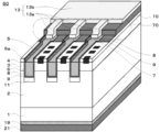
まず、本実施の形態における半導体装置の構成について説明する。図1は、本実施の形態における半導体装置の概略構成を示す平面模式図である。図1に示すように、半導体装置には半導体装置の動作状態において主電流が流れる領域である活性領域40およびその外側の領域である終端領域50が設けられている。ここで、簡潔な説明のために、フィールド絶縁膜10および表面電極20などの図示は省略している。
Ion Etching)によってゲートトレンチ6および終端トレンチ7に対応する位置が開口したエッチングマスク22を形成する。そして、RIEによってゲートトレンチ6、および終端トレンチ7を形成する。このようにして、図4の状態となる。
実施の形態1では、第1ゲート電極9と第2ゲート電極13との接続部において、第2ゲート電極13は分岐しない例を示したが、本実施の形態においては、第2ゲート電極13が分岐した、つまり互いに離隔する複数の引き出し部を有した例について説明する。これ以外の構成は実施の形態1と同様である。
実施の形態1では、平面視でゲートトレンチ6はストライプ状に設けられる例を示したが、本実施の形態においては、平面視でゲートトレンチ6は格子状に設けられる例について説明する。これ以外の構成は実施の形態1と同様である。
Claims (15)
- 第1導電型のドリフト層と、
前記ドリフト層の表層に設けられる第2導電型のウェル領域と、
前記ウェル領域の表層に設けられる第1導電型の不純物領域と、
前記不純物領域の表面から前記ウェル領域を貫通して前記ドリフト層まで達するゲートトレンチと、
平面視で前記ゲートトレンチにつながり、前記ゲートトレンチの延伸方向における幅が、前記ゲートトレンチの幅よりも広い終端トレンチと、
前記ゲートトレンチと前記終端トレンチとの内側の面に接して形成されるゲート絶縁膜と、
前記ゲートトレンチと前記終端トレンチとの内壁および底面に前記ゲート絶縁膜を介して形成される第1ゲート電極と、
前記終端トレンチに形成された前記第1ゲート電極に接し、前記延伸方向において前記ゲートトレンチから遠い方の前記終端トレンチの上端角部の上方を覆って前記終端トレンチの内側から外側に渡り形成され、厚さが前記ゲート絶縁膜の厚さよりも厚いフィールド絶縁膜と、
前記フィールド絶縁膜の上と前記終端トレンチに形成される前記第1ゲート電極の上とに接し、前記延伸方向において前記終端トレンチの内側から外側に渡って前記フィールド絶縁膜に乗り上げる第2ゲート電極と
を備え、
前記フィールド絶縁膜は、前記ゲートトレンチから近い方の前記終端トレンチの上端角部の上方を覆わない、半導体装置。 - 前記第2ゲート電極は、
互いに離隔して複数形成され、前記フィールド絶縁膜の上と前記終端トレンチに形成される前記第1ゲート電極の上とに接し、前記延伸方向において前記終端トレンチの内側から外側に渡って前記フィールド絶縁膜に乗り上げる、第2ゲート電極引き出し部と、
前記フィールド絶縁膜の上に形成され、前記第2ゲート電極引き出し部に接する第2ゲート電極外周部と
を有することを特徴とする、請求項1に記載の半導体装置。 - 前記終端トレンチの外側の層間絶縁膜に設けた前記第2ゲート電極に達するゲートコンタクトホールを介して、前記第2ゲート電極に接続されるゲートパッドをさらに備えることを特徴とする、請求項1または請求項2に記載の半導体装置。
- 前記第2ゲート電極は、平面視で前記ゲートトレンチを取り囲むことを特徴とする、請求項1から請求項3のいずれか一項に記載の半導体装置。
- 前記終端トレンチの前記延伸方向における幅は、前記ゲートトレンチの幅の3倍以下であることを特徴とする、請求項1から請求項4のいずれか一項に記載の半導体装置。
- 前記フィールド絶縁膜の厚さは、前記ゲート絶縁膜の厚さの2倍以上であることを特徴とする、請求項1から請求項5のいずれか一項に記載の半導体装置。
- 断面視で前記終端トレンチに形成される前記第1ゲート電極の上端は前記終端トレンチの上端よりも下方に位置することを特徴とする、請求項1から請求項6のいずれか一項に記載の半導体装置。
- 前記第1ゲート電極と前記第2ゲート電極とはそれぞれ異なる材料で構成されることを特徴とする、請求項1から請求項7のいずれか一項に記載の半導体装置。
- 前記ゲートトレンチはストライプ状または格子状に設けられることを特徴とする、請求項1から請求項8のいずれか一項に記載の半導体装置。
- 前記ゲートトレンチの底面と前記終端トレンチの底面との下方の少なくとも一方に、第2導電型の電界緩和領域が設けられることを特徴とする、請求項1から請求項9のいずれか一項に記載の半導体装置。
- 第1導電型のドリフト層を形成する工程と、
前記ドリフト層の表層に第2導電型のウェル領域を設ける工程と、
前記ウェル領域の表層に第1導電型の不純物領域を設ける工程と、
前記不純物領域の表面から前記ウェル領域を貫通して前記ドリフト層まで達するゲートトレンチを設ける工程と、
平面視で前記ゲートトレンチにつながり、前記ゲートトレンチの延伸方向における幅が前記ゲートトレンチの幅よりも広い終端トレンチを設ける工程と、
前記ゲートトレンチと前記終端トレンチとの内壁および底面に接するゲート絶縁膜を形成する工程と、
前記ゲートトレンチと前記終端トレンチとの内側に前記ゲート絶縁膜を介して第1ゲート電極を形成する工程と、
前記終端トレンチに形成された前記第1ゲート電極に接し、前記延伸方向において前記ゲートトレンチから遠い方の前記終端トレンチの上端角部の上方を覆って前記終端トレンチの内側から外側に渡り、厚さを前記ゲート絶縁膜の厚さよりも厚くしたフィールド絶縁膜を形成する工程と、
前記フィールド絶縁膜の上と前記終端トレンチに形成される前記第1ゲート電極の上とに接し、前記延伸方向において前記終端トレンチの内側から外側に渡って前記フィールド絶縁膜に乗り上げる第2ゲート電極を形成する工程と
を備え、
前記フィールド絶縁膜を形成する工程において、前記フィールド絶縁膜は、前記ゲートトレンチから近い方の前記終端トレンチの上端角部の上方を覆わないように形成される、半導体装置の製造方法。 - 前記フィールド絶縁膜は、反応性イオンエッチングまたはウェットエッチングによりパターニングされて形成されることを特徴とする、請求項11に記載の半導体装置の製造方法。
- 前記フィールド絶縁膜は、CVD法により形成されることを特徴とする、請求項11または請求項12に記載の半導体装置の製造方法。
- 前記第1ゲート電極は、断面視で前記終端トレンチの上端よりも下方に位置するように、エッチバックにより形成されることを特徴とする、請求項11から請求項13のいずれか一項に記載の半導体装置の製造方法。
- 前記第2ゲート電極と前記終端トレンチに形成された前記第1ゲート電極との上に層間絶縁膜を形成する工程と、
前記終端トレンチの外側の前記層間絶縁膜に、前記第2ゲート電極に達するゲートコンタクトホールを設ける工程と、
前記ゲートコンタクトホールを介して前記第2ゲート電極の上に、ゲートパッドを形成する工程と
をさらに備えることを特徴とする、請求項11から請求項14のいずれか一項に記載の半導体装置の製造方法。
Applications Claiming Priority (1)
| Application Number | Priority Date | Filing Date | Title |
|---|---|---|---|
| PCT/JP2022/009146 WO2023166666A1 (ja) | 2022-03-03 | 2022-03-03 | 半導体装置および半導体装置の製造方法 |
Publications (3)
| Publication Number | Publication Date |
|---|---|
| JP7338813B1 true JP7338813B1 (ja) | 2023-09-05 |
| JPWO2023166666A1 JPWO2023166666A1 (ja) | 2023-09-07 |
| JPWO2023166666A5 JPWO2023166666A5 (ja) | 2024-02-06 |
Family
ID=87882198
Family Applications (1)
| Application Number | Title | Priority Date | Filing Date |
|---|---|---|---|
| JP2023524727A Active JP7338813B1 (ja) | 2022-03-03 | 2022-03-03 | 半導体装置および半導体装置の製造方法 |
Country Status (2)
| Country | Link |
|---|---|
| JP (1) | JP7338813B1 (ja) |
| WO (1) | WO2023166666A1 (ja) |
Citations (6)
| Publication number | Priority date | Publication date | Assignee | Title |
|---|---|---|---|---|
| JP2001177093A (ja) * | 1999-12-20 | 2001-06-29 | Toyota Central Res & Dev Lab Inc | 絶縁ゲート型半導体装置 |
| JP2009505433A (ja) * | 2005-08-17 | 2009-02-05 | インターナショナル レクティファイアー コーポレイション | ゲートトレンチで相互接続されたパワー半導体デバイス |
| JP2009522807A (ja) * | 2006-01-05 | 2009-06-11 | フェアチャイルド・セミコンダクター・コーポレーション | 化学的機械式平坦化を利用したパワーデバイス |
| WO2016047438A1 (ja) * | 2014-09-26 | 2016-03-31 | 三菱電機株式会社 | 半導体装置 |
| WO2018163286A1 (ja) * | 2017-03-07 | 2018-09-13 | 三菱電機株式会社 | 半導体装置および電力変換装置 |
| JP2019161199A (ja) * | 2017-05-17 | 2019-09-19 | ローム株式会社 | 半導体装置 |
-
2022
- 2022-03-03 JP JP2023524727A patent/JP7338813B1/ja active Active
- 2022-03-03 WO PCT/JP2022/009146 patent/WO2023166666A1/ja active Application Filing
Patent Citations (6)
| Publication number | Priority date | Publication date | Assignee | Title |
|---|---|---|---|---|
| JP2001177093A (ja) * | 1999-12-20 | 2001-06-29 | Toyota Central Res & Dev Lab Inc | 絶縁ゲート型半導体装置 |
| JP2009505433A (ja) * | 2005-08-17 | 2009-02-05 | インターナショナル レクティファイアー コーポレイション | ゲートトレンチで相互接続されたパワー半導体デバイス |
| JP2009522807A (ja) * | 2006-01-05 | 2009-06-11 | フェアチャイルド・セミコンダクター・コーポレーション | 化学的機械式平坦化を利用したパワーデバイス |
| WO2016047438A1 (ja) * | 2014-09-26 | 2016-03-31 | 三菱電機株式会社 | 半導体装置 |
| WO2018163286A1 (ja) * | 2017-03-07 | 2018-09-13 | 三菱電機株式会社 | 半導体装置および電力変換装置 |
| JP2019161199A (ja) * | 2017-05-17 | 2019-09-19 | ローム株式会社 | 半導体装置 |
Also Published As
| Publication number | Publication date |
|---|---|
| WO2023166666A1 (ja) | 2023-09-07 |
| JPWO2023166666A1 (ja) | 2023-09-07 |
Similar Documents
| Publication | Publication Date | Title |
|---|---|---|
| JP5525940B2 (ja) | 半導体装置および半導体装置の製造方法 | |
| JP5588670B2 (ja) | 半導体装置 | |
| WO2013118203A1 (ja) | 半導体装置及びその製造方法 | |
| JP7029710B2 (ja) | 半導体装置 | |
| JP6705155B2 (ja) | 半導体装置および半導体装置の製造方法 | |
| JP2018019046A (ja) | 炭化ケイ素半導体装置および炭化ケイ素半導体装置の製造方法 | |
| JP2019003967A (ja) | 半導体装置および半導体装置の製造方法 | |
| US10439027B2 (en) | Silicon carbide semiconductor device and method for manufacturing the same | |
| JP2018116986A (ja) | 半導体装置および半導体装置の製造方法 | |
| JP7155641B2 (ja) | 半導体装置 | |
| CN112466752A (zh) | 碳化硅半导体装置及碳化硅半导体装置的制造方法 | |
| JP2014127547A (ja) | 半導体装置の製造方法 | |
| TWI702722B (zh) | 半導體裝置及半導體裝置之製造方法 | |
| JP6648852B1 (ja) | 炭化珪素半導体装置および炭化珪素半導体装置の製造方法 | |
| JP7338813B1 (ja) | 半導体装置および半導体装置の製造方法 | |
| JP6771433B2 (ja) | 半導体装置 | |
| KR101965550B1 (ko) | 반도체 장치 | |
| JP2019033140A (ja) | 半導体装置および半導体装置の製造方法 | |
| WO2024053022A1 (ja) | 半導体装置およびその製造方法 | |
| CN113161232A (zh) | 碳化硅半导体装置的制造方法 | |
| JP2022007788A (ja) | 半導体装置 | |
| JP2014241426A (ja) | 半導体装置 | |
| JP7330392B2 (ja) | 半導体装置および半導体装置の製造方法 | |
| JP5223041B1 (ja) | 半導体装置及びその製造方法 | |
| US20230246077A1 (en) | Silicon carbide semiconductor device and method of manufacturing silicon carbide semiconductor device |
Legal Events
| Date | Code | Title | Description |
|---|---|---|---|
| A521 | Request for written amendment filed |
Free format text: JAPANESE INTERMEDIATE CODE: A523 Effective date: 20230421 |
|
| A621 | Written request for application examination |
Free format text: JAPANESE INTERMEDIATE CODE: A621 Effective date: 20230421 |
|
| A871 | Explanation of circumstances concerning accelerated examination |
Free format text: JAPANESE INTERMEDIATE CODE: A871 Effective date: 20230421 |
|
| TRDD | Decision of grant or rejection written | ||
| A01 | Written decision to grant a patent or to grant a registration (utility model) |
Free format text: JAPANESE INTERMEDIATE CODE: A01 Effective date: 20230725 |
|
| A61 | First payment of annual fees (during grant procedure) |
Free format text: JAPANESE INTERMEDIATE CODE: A61 Effective date: 20230807 |
|
| R151 | Written notification of patent or utility model registration |
Ref document number: 7338813 Country of ref document: JP Free format text: JAPANESE INTERMEDIATE CODE: R151 |