JP7155455B2 - Vcselモジュール - Google Patents
Vcselモジュール Download PDFInfo
- Publication number
- JP7155455B2 JP7155455B2 JP2022516276A JP2022516276A JP7155455B2 JP 7155455 B2 JP7155455 B2 JP 7155455B2 JP 2022516276 A JP2022516276 A JP 2022516276A JP 2022516276 A JP2022516276 A JP 2022516276A JP 7155455 B2 JP7155455 B2 JP 7155455B2
- Authority
- JP
- Japan
- Prior art keywords
- vcsel
- terminal
- electrode
- semiconductor device
- module
- Prior art date
- Legal status (The legal status is an assumption and is not a legal conclusion. Google has not performed a legal analysis and makes no representation as to the accuracy of the status listed.)
- Expired - Fee Related
Links
Images


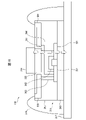


Classifications
-
- H—ELECTRICITY
- H01—ELECTRIC ELEMENTS
- H01S—DEVICES USING THE PROCESS OF LIGHT AMPLIFICATION BY STIMULATED EMISSION OF RADIATION [LASER] TO AMPLIFY OR GENERATE LIGHT; DEVICES USING STIMULATED EMISSION OF ELECTROMAGNETIC RADIATION IN WAVE RANGES OTHER THAN OPTICAL
- H01S5/00—Semiconductor lasers
- H01S5/02—Structural details or components not essential to laser action
- H01S5/022—Mountings; Housings
- H01S5/0239—Combinations of electrical or optical elements
-
- G—PHYSICS
- G01—MEASURING; TESTING
- G01S—RADIO DIRECTION-FINDING; RADIO NAVIGATION; DETERMINING DISTANCE OR VELOCITY BY USE OF RADIO WAVES; LOCATING OR PRESENCE-DETECTING BY USE OF THE REFLECTION OR RERADIATION OF RADIO WAVES; ANALOGOUS ARRANGEMENTS USING OTHER WAVES
- G01S17/00—Systems using the reflection or reradiation of electromagnetic waves other than radio waves, e.g. lidar systems
- G01S17/02—Systems using the reflection of electromagnetic waves other than radio waves
- G01S17/06—Systems determining position data of a target
- G01S17/08—Systems determining position data of a target for measuring distance only
- G01S17/10—Systems determining position data of a target for measuring distance only using transmission of interrupted, pulse-modulated waves
-
- G—PHYSICS
- G01—MEASURING; TESTING
- G01S—RADIO DIRECTION-FINDING; RADIO NAVIGATION; DETERMINING DISTANCE OR VELOCITY BY USE OF RADIO WAVES; LOCATING OR PRESENCE-DETECTING BY USE OF THE REFLECTION OR RERADIATION OF RADIO WAVES; ANALOGOUS ARRANGEMENTS USING OTHER WAVES
- G01S7/00—Details of systems according to groups G01S13/00, G01S15/00, G01S17/00
- G01S7/48—Details of systems according to groups G01S13/00, G01S15/00, G01S17/00 of systems according to group G01S17/00
- G01S7/483—Details of pulse systems
- G01S7/484—Transmitters
-
- H—ELECTRICITY
- H01—ELECTRIC ELEMENTS
- H01S—DEVICES USING THE PROCESS OF LIGHT AMPLIFICATION BY STIMULATED EMISSION OF RADIATION [LASER] TO AMPLIFY OR GENERATE LIGHT; DEVICES USING STIMULATED EMISSION OF ELECTROMAGNETIC RADIATION IN WAVE RANGES OTHER THAN OPTICAL
- H01S5/00—Semiconductor lasers
- H01S5/02—Structural details or components not essential to laser action
- H01S5/022—Mountings; Housings
- H01S5/023—Mount members, e.g. sub-mount members
- H01S5/02325—Mechanically integrated components on mount members or optical micro-benches
-
- H—ELECTRICITY
- H01—ELECTRIC ELEMENTS
- H01S—DEVICES USING THE PROCESS OF LIGHT AMPLIFICATION BY STIMULATED EMISSION OF RADIATION [LASER] TO AMPLIFY OR GENERATE LIGHT; DEVICES USING STIMULATED EMISSION OF ELECTROMAGNETIC RADIATION IN WAVE RANGES OTHER THAN OPTICAL
- H01S5/00—Semiconductor lasers
- H01S5/02—Structural details or components not essential to laser action
- H01S5/022—Mountings; Housings
- H01S5/0233—Mounting configuration of laser chips
- H01S5/02345—Wire-bonding
-
- H—ELECTRICITY
- H01—ELECTRIC ELEMENTS
- H01S—DEVICES USING THE PROCESS OF LIGHT AMPLIFICATION BY STIMULATED EMISSION OF RADIATION [LASER] TO AMPLIFY OR GENERATE LIGHT; DEVICES USING STIMULATED EMISSION OF ELECTROMAGNETIC RADIATION IN WAVE RANGES OTHER THAN OPTICAL
- H01S5/00—Semiconductor lasers
- H01S5/02—Structural details or components not essential to laser action
- H01S5/024—Arrangements for thermal management
- H01S5/02469—Passive cooling, e.g. where heat is removed by the housing as a whole or by a heat pipe without any active cooling element like a TEC
-
- H—ELECTRICITY
- H01—ELECTRIC ELEMENTS
- H01S—DEVICES USING THE PROCESS OF LIGHT AMPLIFICATION BY STIMULATED EMISSION OF RADIATION [LASER] TO AMPLIFY OR GENERATE LIGHT; DEVICES USING STIMULATED EMISSION OF ELECTROMAGNETIC RADIATION IN WAVE RANGES OTHER THAN OPTICAL
- H01S5/00—Semiconductor lasers
- H01S5/04—Processes or apparatus for excitation, e.g. pumping, e.g. by electron beams
- H01S5/042—Electrical excitation ; Circuits therefor
-
- H—ELECTRICITY
- H01—ELECTRIC ELEMENTS
- H01S—DEVICES USING THE PROCESS OF LIGHT AMPLIFICATION BY STIMULATED EMISSION OF RADIATION [LASER] TO AMPLIFY OR GENERATE LIGHT; DEVICES USING STIMULATED EMISSION OF ELECTROMAGNETIC RADIATION IN WAVE RANGES OTHER THAN OPTICAL
- H01S5/00—Semiconductor lasers
- H01S5/04—Processes or apparatus for excitation, e.g. pumping, e.g. by electron beams
- H01S5/042—Electrical excitation ; Circuits therefor
- H01S5/0425—Electrodes, e.g. characterised by the structure
- H01S5/04256—Electrodes, e.g. characterised by the structure characterised by the configuration
-
- H—ELECTRICITY
- H01—ELECTRIC ELEMENTS
- H01S—DEVICES USING THE PROCESS OF LIGHT AMPLIFICATION BY STIMULATED EMISSION OF RADIATION [LASER] TO AMPLIFY OR GENERATE LIGHT; DEVICES USING STIMULATED EMISSION OF ELECTROMAGNETIC RADIATION IN WAVE RANGES OTHER THAN OPTICAL
- H01S5/00—Semiconductor lasers
- H01S5/04—Processes or apparatus for excitation, e.g. pumping, e.g. by electron beams
- H01S5/042—Electrical excitation ; Circuits therefor
- H01S5/0428—Electrical excitation ; Circuits therefor for applying pulses to the laser
-
- H—ELECTRICITY
- H01—ELECTRIC ELEMENTS
- H01S—DEVICES USING THE PROCESS OF LIGHT AMPLIFICATION BY STIMULATED EMISSION OF RADIATION [LASER] TO AMPLIFY OR GENERATE LIGHT; DEVICES USING STIMULATED EMISSION OF ELECTROMAGNETIC RADIATION IN WAVE RANGES OTHER THAN OPTICAL
- H01S5/00—Semiconductor lasers
- H01S5/06—Arrangements for controlling the laser output parameters, e.g. by operating on the active medium
- H01S5/062—Arrangements for controlling the laser output parameters, e.g. by operating on the active medium by varying the potential of the electrodes
- H01S5/06226—Modulation at ultra-high frequencies
-
- H—ELECTRICITY
- H01—ELECTRIC ELEMENTS
- H01S—DEVICES USING THE PROCESS OF LIGHT AMPLIFICATION BY STIMULATED EMISSION OF RADIATION [LASER] TO AMPLIFY OR GENERATE LIGHT; DEVICES USING STIMULATED EMISSION OF ELECTROMAGNETIC RADIATION IN WAVE RANGES OTHER THAN OPTICAL
- H01S5/00—Semiconductor lasers
- H01S5/40—Arrangement of two or more semiconductor lasers, not provided for in groups H01S5/02 - H01S5/30
- H01S5/42—Arrays of surface emitting lasers
- H01S5/423—Arrays of surface emitting lasers having a vertical cavity
-
- H—ELECTRICITY
- H10—SEMICONDUCTOR DEVICES; ELECTRIC SOLID-STATE DEVICES NOT OTHERWISE PROVIDED FOR
- H10W—GENERIC PACKAGES, INTERCONNECTIONS, CONNECTORS OR OTHER CONSTRUCTIONAL DETAILS OF DEVICES COVERED BY CLASS H10
- H10W90/00—Package configurations
-
- H—ELECTRICITY
- H01—ELECTRIC ELEMENTS
- H01S—DEVICES USING THE PROCESS OF LIGHT AMPLIFICATION BY STIMULATED EMISSION OF RADIATION [LASER] TO AMPLIFY OR GENERATE LIGHT; DEVICES USING STIMULATED EMISSION OF ELECTROMAGNETIC RADIATION IN WAVE RANGES OTHER THAN OPTICAL
- H01S5/00—Semiconductor lasers
- H01S5/10—Construction or shape of the optical resonator, e.g. extended or external cavity, coupled cavities, bent-guide, varying width, thickness or composition of the active region
- H01S5/18—Surface-emitting [SE] lasers, e.g. having both horizontal and vertical cavities
- H01S5/183—Surface-emitting [SE] lasers, e.g. having both horizontal and vertical cavities having only vertical cavities, e.g. vertical cavity surface-emitting lasers [VCSEL]
-
- H—ELECTRICITY
- H10—SEMICONDUCTOR DEVICES; ELECTRIC SOLID-STATE DEVICES NOT OTHERWISE PROVIDED FOR
- H10W—GENERIC PACKAGES, INTERCONNECTIONS, CONNECTORS OR OTHER CONSTRUCTIONAL DETAILS OF DEVICES COVERED BY CLASS H10
- H10W72/00—Interconnections or connectors in packages
- H10W72/071—Connecting or disconnecting
- H10W72/073—Connecting or disconnecting of die-attach connectors
-
- H—ELECTRICITY
- H10—SEMICONDUCTOR DEVICES; ELECTRIC SOLID-STATE DEVICES NOT OTHERWISE PROVIDED FOR
- H10W—GENERIC PACKAGES, INTERCONNECTIONS, CONNECTORS OR OTHER CONSTRUCTIONAL DETAILS OF DEVICES COVERED BY CLASS H10
- H10W72/00—Interconnections or connectors in packages
- H10W72/071—Connecting or disconnecting
- H10W72/075—Connecting or disconnecting of bond wires
-
- H—ELECTRICITY
- H10—SEMICONDUCTOR DEVICES; ELECTRIC SOLID-STATE DEVICES NOT OTHERWISE PROVIDED FOR
- H10W—GENERIC PACKAGES, INTERCONNECTIONS, CONNECTORS OR OTHER CONSTRUCTIONAL DETAILS OF DEVICES COVERED BY CLASS H10
- H10W72/00—Interconnections or connectors in packages
- H10W72/50—Bond wires
- H10W72/541—Dispositions of bond wires
- H10W72/5445—Dispositions of bond wires being orthogonal to a side surface of the chip, e.g. parallel arrangements
-
- H—ELECTRICITY
- H10—SEMICONDUCTOR DEVICES; ELECTRIC SOLID-STATE DEVICES NOT OTHERWISE PROVIDED FOR
- H10W—GENERIC PACKAGES, INTERCONNECTIONS, CONNECTORS OR OTHER CONSTRUCTIONAL DETAILS OF DEVICES COVERED BY CLASS H10
- H10W72/00—Interconnections or connectors in packages
- H10W72/851—Dispositions of multiple connectors or interconnections
- H10W72/874—On different surfaces
- H10W72/884—Die-attach connectors and bond wires
-
- H—ELECTRICITY
- H10—SEMICONDUCTOR DEVICES; ELECTRIC SOLID-STATE DEVICES NOT OTHERWISE PROVIDED FOR
- H10W—GENERIC PACKAGES, INTERCONNECTIONS, CONNECTORS OR OTHER CONSTRUCTIONAL DETAILS OF DEVICES COVERED BY CLASS H10
- H10W74/00—Encapsulations, e.g. protective coatings
- H10W74/10—Encapsulations, e.g. protective coatings characterised by their shape or disposition
-
- H—ELECTRICITY
- H10—SEMICONDUCTOR DEVICES; ELECTRIC SOLID-STATE DEVICES NOT OTHERWISE PROVIDED FOR
- H10W—GENERIC PACKAGES, INTERCONNECTIONS, CONNECTORS OR OTHER CONSTRUCTIONAL DETAILS OF DEVICES COVERED BY CLASS H10
- H10W90/00—Package configurations
- H10W90/701—Package configurations characterised by the relative positions of pads or connectors relative to package parts
- H10W90/721—Package configurations characterised by the relative positions of pads or connectors relative to package parts of bump connectors
- H10W90/724—Package configurations characterised by the relative positions of pads or connectors relative to package parts of bump connectors between a chip and a stacked insulating package substrate, interposer or RDL
-
- H—ELECTRICITY
- H10—SEMICONDUCTOR DEVICES; ELECTRIC SOLID-STATE DEVICES NOT OTHERWISE PROVIDED FOR
- H10W—GENERIC PACKAGES, INTERCONNECTIONS, CONNECTORS OR OTHER CONSTRUCTIONAL DETAILS OF DEVICES COVERED BY CLASS H10
- H10W90/00—Package configurations
- H10W90/701—Package configurations characterised by the relative positions of pads or connectors relative to package parts
- H10W90/731—Package configurations characterised by the relative positions of pads or connectors relative to package parts of die-attach connectors
- H10W90/732—Package configurations characterised by the relative positions of pads or connectors relative to package parts of die-attach connectors between stacked chips
-
- H—ELECTRICITY
- H10—SEMICONDUCTOR DEVICES; ELECTRIC SOLID-STATE DEVICES NOT OTHERWISE PROVIDED FOR
- H10W—GENERIC PACKAGES, INTERCONNECTIONS, CONNECTORS OR OTHER CONSTRUCTIONAL DETAILS OF DEVICES COVERED BY CLASS H10
- H10W90/00—Package configurations
- H10W90/701—Package configurations characterised by the relative positions of pads or connectors relative to package parts
- H10W90/751—Package configurations characterised by the relative positions of pads or connectors relative to package parts of bond wires
- H10W90/752—Package configurations characterised by the relative positions of pads or connectors relative to package parts of bond wires between stacked chips
-
- H—ELECTRICITY
- H10—SEMICONDUCTOR DEVICES; ELECTRIC SOLID-STATE DEVICES NOT OTHERWISE PROVIDED FOR
- H10W—GENERIC PACKAGES, INTERCONNECTIONS, CONNECTORS OR OTHER CONSTRUCTIONAL DETAILS OF DEVICES COVERED BY CLASS H10
- H10W90/00—Package configurations
- H10W90/701—Package configurations characterised by the relative positions of pads or connectors relative to package parts
- H10W90/751—Package configurations characterised by the relative positions of pads or connectors relative to package parts of bond wires
- H10W90/754—Package configurations characterised by the relative positions of pads or connectors relative to package parts of bond wires between a chip and a stacked insulating package substrate, interposer or RDL
Landscapes
- Physics & Mathematics (AREA)
- General Physics & Mathematics (AREA)
- Electromagnetism (AREA)
- Condensed Matter Physics & Semiconductors (AREA)
- Optics & Photonics (AREA)
- Engineering & Computer Science (AREA)
- Computer Networks & Wireless Communication (AREA)
- Radar, Positioning & Navigation (AREA)
- Remote Sensing (AREA)
- Semiconductor Lasers (AREA)
Priority Applications (1)
| Application Number | Priority Date | Filing Date | Title |
|---|---|---|---|
| JP2022161135A JP7628993B2 (ja) | 2020-06-22 | 2022-10-05 | Vcselモジュール |
Applications Claiming Priority (5)
| Application Number | Priority Date | Filing Date | Title |
|---|---|---|---|
| JP2020107020 | 2020-06-22 | ||
| JP2020107020 | 2020-06-22 | ||
| JP2021052423 | 2021-03-25 | ||
| JP2021052423 | 2021-03-25 | ||
| PCT/JP2021/023664 WO2021261496A1 (ja) | 2020-06-22 | 2021-06-22 | Vcselモジュール |
Related Child Applications (1)
| Application Number | Title | Priority Date | Filing Date |
|---|---|---|---|
| JP2022161135A Division JP7628993B2 (ja) | 2020-06-22 | 2022-10-05 | Vcselモジュール |
Publications (3)
| Publication Number | Publication Date |
|---|---|
| JPWO2021261496A1 JPWO2021261496A1 (cg-RX-API-DMAC7.html) | 2021-12-30 |
| JPWO2021261496A5 JPWO2021261496A5 (cg-RX-API-DMAC7.html) | 2022-06-10 |
| JP7155455B2 true JP7155455B2 (ja) | 2022-10-18 |
Family
ID=79281242
Family Applications (2)
| Application Number | Title | Priority Date | Filing Date |
|---|---|---|---|
| JP2022516276A Expired - Fee Related JP7155455B2 (ja) | 2020-06-22 | 2021-06-22 | Vcselモジュール |
| JP2022161135A Active JP7628993B2 (ja) | 2020-06-22 | 2022-10-05 | Vcselモジュール |
Family Applications After (1)
| Application Number | Title | Priority Date | Filing Date |
|---|---|---|---|
| JP2022161135A Active JP7628993B2 (ja) | 2020-06-22 | 2022-10-05 | Vcselモジュール |
Country Status (4)
| Country | Link |
|---|---|
| US (1) | US20240243546A1 (cg-RX-API-DMAC7.html) |
| JP (2) | JP7155455B2 (cg-RX-API-DMAC7.html) |
| CN (1) | CN115943533A (cg-RX-API-DMAC7.html) |
| WO (1) | WO2021261496A1 (cg-RX-API-DMAC7.html) |
Families Citing this family (1)
| Publication number | Priority date | Publication date | Assignee | Title |
|---|---|---|---|---|
| CN116316052A (zh) * | 2023-03-22 | 2023-06-23 | 宁波飞芯电子科技有限公司 | 垂直腔面发射激光器、探测设备及探测系统 |
Citations (10)
| Publication number | Priority date | Publication date | Assignee | Title |
|---|---|---|---|---|
| JP2010531546A (ja) | 2007-06-27 | 2010-09-24 | コーニンクレッカ フィリップス エレクトロニクス エヌ ヴィ | 光センサ・モジュール及びその製造方法 |
| JP2012037276A (ja) | 2010-08-04 | 2012-02-23 | Sharp Corp | 光学式測距装置 |
| WO2014017256A1 (ja) | 2012-07-24 | 2014-01-30 | シャープ株式会社 | 光学式測距装置および電子機器 |
| WO2018100082A1 (en) | 2016-11-30 | 2018-06-07 | Sony Semiconductor Solutions Corporation | Apparatus and method |
| US20180278011A1 (en) | 2017-03-23 | 2018-09-27 | Infineon Technologies Ag | Laser diode module |
| JP2019158693A (ja) | 2018-03-15 | 2019-09-19 | 株式会社リコー | 受光装置、物体検出装置、距離測定装置、移動体装置、ノイズ計測方法、物体検出方法及び距離測定方法 |
| US20200006271A1 (en) | 2018-07-02 | 2020-01-02 | Taiwan Semiconductor Manufacturing Co., Ltd. | Structures for bonding a group iii-v device to a substrate |
| WO2020044817A1 (ja) | 2018-08-31 | 2020-03-05 | ソニーセミコンダクタソリューションズ株式会社 | 光源装置、検出方法、センシングモジュール |
| WO2020054257A1 (ja) | 2018-09-11 | 2020-03-19 | ソニーセミコンダクタソリューションズ株式会社 | 光源装置、センシングモジュール |
| US20200185875A1 (en) | 2018-12-06 | 2020-06-11 | Finisar Corporation | Optoelectronic assembly |
Family Cites Families (13)
| Publication number | Priority date | Publication date | Assignee | Title |
|---|---|---|---|---|
| JPH06203403A (ja) * | 1992-10-22 | 1994-07-22 | Matsushita Electron Corp | 半導体レーザ装置および光ピックアップ装置 |
| JPH06237016A (ja) * | 1993-02-09 | 1994-08-23 | Matsushita Electric Ind Co Ltd | 光ファイバモジュールおよびその製造方法 |
| JP3831631B2 (ja) * | 2000-09-29 | 2006-10-11 | 三洋電機株式会社 | 受光素子及びそれを備える光半導体装置 |
| JP2004031456A (ja) * | 2002-06-21 | 2004-01-29 | Fujitsu Ltd | 光インタコネクション装置及びインタコネクションモジュール |
| US20070200512A1 (en) * | 2004-04-21 | 2007-08-30 | Matsushita Electric Industrial Co., Ltd. | Semiconductor Chip For Driving Light Emitting Element, Light Emitting Device And Lighting Equipment |
| JP5034368B2 (ja) * | 2006-08-17 | 2012-09-26 | 富士ゼロックス株式会社 | 高周波特性が改善された表面発光型半導体レーザ素子 |
| JP2009008721A (ja) * | 2007-06-26 | 2009-01-15 | Fuji Xerox Co Ltd | 光モジュール、光電気複合基板、光信号伝送装置及び画像形成装置 |
| JP2009105240A (ja) * | 2007-10-24 | 2009-05-14 | Fuji Xerox Co Ltd | 半導体発光装置 |
| US8488921B2 (en) * | 2010-07-16 | 2013-07-16 | International Business Machines Corporation | Packaged multicore fiber optical transceiver module |
| JP5952101B2 (ja) * | 2012-06-20 | 2016-07-13 | 日本特殊陶業株式会社 | 光電気混載ユニット、素子搭載モジュール |
| JP6280002B2 (ja) * | 2014-08-22 | 2018-02-14 | 浜松ホトニクス株式会社 | 測距方法及び測距装置 |
| EP3764487A4 (en) * | 2018-03-08 | 2021-12-01 | Kyocera Corporation | SUBSTRATE FOR THE ASSEMBLY OF A LIGHT EMITTING ELEMENT AND LIGHT EMITTING DEVICE |
| JP2021114556A (ja) * | 2020-01-20 | 2021-08-05 | ソニーセミコンダクタソリューションズ株式会社 | 発光装置およびその製造方法 |
-
2021
- 2021-06-22 JP JP2022516276A patent/JP7155455B2/ja not_active Expired - Fee Related
- 2021-06-22 CN CN202180044387.9A patent/CN115943533A/zh active Pending
- 2021-06-22 US US18/012,628 patent/US20240243546A1/en not_active Abandoned
- 2021-06-22 WO PCT/JP2021/023664 patent/WO2021261496A1/ja not_active Ceased
-
2022
- 2022-10-05 JP JP2022161135A patent/JP7628993B2/ja active Active
Patent Citations (10)
| Publication number | Priority date | Publication date | Assignee | Title |
|---|---|---|---|---|
| JP2010531546A (ja) | 2007-06-27 | 2010-09-24 | コーニンクレッカ フィリップス エレクトロニクス エヌ ヴィ | 光センサ・モジュール及びその製造方法 |
| JP2012037276A (ja) | 2010-08-04 | 2012-02-23 | Sharp Corp | 光学式測距装置 |
| WO2014017256A1 (ja) | 2012-07-24 | 2014-01-30 | シャープ株式会社 | 光学式測距装置および電子機器 |
| WO2018100082A1 (en) | 2016-11-30 | 2018-06-07 | Sony Semiconductor Solutions Corporation | Apparatus and method |
| US20180278011A1 (en) | 2017-03-23 | 2018-09-27 | Infineon Technologies Ag | Laser diode module |
| JP2019158693A (ja) | 2018-03-15 | 2019-09-19 | 株式会社リコー | 受光装置、物体検出装置、距離測定装置、移動体装置、ノイズ計測方法、物体検出方法及び距離測定方法 |
| US20200006271A1 (en) | 2018-07-02 | 2020-01-02 | Taiwan Semiconductor Manufacturing Co., Ltd. | Structures for bonding a group iii-v device to a substrate |
| WO2020044817A1 (ja) | 2018-08-31 | 2020-03-05 | ソニーセミコンダクタソリューションズ株式会社 | 光源装置、検出方法、センシングモジュール |
| WO2020054257A1 (ja) | 2018-09-11 | 2020-03-19 | ソニーセミコンダクタソリューションズ株式会社 | 光源装置、センシングモジュール |
| US20200185875A1 (en) | 2018-12-06 | 2020-06-11 | Finisar Corporation | Optoelectronic assembly |
Also Published As
| Publication number | Publication date |
|---|---|
| JPWO2021261496A1 (cg-RX-API-DMAC7.html) | 2021-12-30 |
| JP2022179619A (ja) | 2022-12-02 |
| JP7628993B2 (ja) | 2025-02-12 |
| US20240243546A1 (en) | 2024-07-18 |
| WO2021261496A1 (ja) | 2021-12-30 |
| CN115943533A (zh) | 2023-04-07 |
Similar Documents
| Publication | Publication Date | Title |
|---|---|---|
| US10490722B2 (en) | Light emitting package having a guiding member guiding an optical member | |
| US7586125B2 (en) | Light emitting diode package structure and fabricating method thereof | |
| US7855396B2 (en) | Light emitting diode package structure | |
| CN100524864C (zh) | 发光二极管封装结构及其制作方法 | |
| US7525124B2 (en) | Submount for light emitting diode and its manufacturing method | |
| JP2003008083A (ja) | 多数チップ半導体ledアセンブリ | |
| JP7628993B2 (ja) | Vcselモジュール | |
| CN107980182B (zh) | 发光装置及其制造方法 | |
| KR101259876B1 (ko) | 열전 소자를 갖는 엘이디 패키지 및 이의 제조 방법 | |
| JP2005294292A (ja) | 発光装置及び発光装置の製造方法 | |
| JP2022167697A (ja) | 発光装置 | |
| JP2022168626A (ja) | 発光装置 | |
| JP2022164487A (ja) | 発光装置 |
Legal Events
| Date | Code | Title | Description |
|---|---|---|---|
| A529 | Written submission of copy of amendment under article 34 pct |
Free format text: JAPANESE INTERMEDIATE CODE: A5211 Effective date: 20220311 |
|
| A621 | Written request for application examination |
Free format text: JAPANESE INTERMEDIATE CODE: A621 Effective date: 20220311 |
|
| A871 | Explanation of circumstances concerning accelerated examination |
Free format text: JAPANESE INTERMEDIATE CODE: A871 Effective date: 20220311 |
|
| A131 | Notification of reasons for refusal |
Free format text: JAPANESE INTERMEDIATE CODE: A131 Effective date: 20220705 |
|
| A521 | Request for written amendment filed |
Free format text: JAPANESE INTERMEDIATE CODE: A523 Effective date: 20220713 |
|
| TRDD | Decision of grant or rejection written | ||
| A01 | Written decision to grant a patent or to grant a registration (utility model) |
Free format text: JAPANESE INTERMEDIATE CODE: A01 Effective date: 20220906 |
|
| A61 | First payment of annual fees (during grant procedure) |
Free format text: JAPANESE INTERMEDIATE CODE: A61 Effective date: 20221005 |
|
| R150 | Certificate of patent or registration of utility model |
Ref document number: 7155455 Country of ref document: JP Free format text: JAPANESE INTERMEDIATE CODE: R150 |
|
| LAPS | Cancellation because of no payment of annual fees |