JP7155455B2 - Vcselモジュール - Google Patents
Vcselモジュール Download PDFInfo
- Publication number
- JP7155455B2 JP7155455B2 JP2022516276A JP2022516276A JP7155455B2 JP 7155455 B2 JP7155455 B2 JP 7155455B2 JP 2022516276 A JP2022516276 A JP 2022516276A JP 2022516276 A JP2022516276 A JP 2022516276A JP 7155455 B2 JP7155455 B2 JP 7155455B2
- Authority
- JP
- Japan
- Prior art keywords
- vcsel
- terminal
- electrode
- semiconductor device
- module
- Prior art date
- Legal status (The legal status is an assumption and is not a legal conclusion. Google has not performed a legal analysis and makes no representation as to the accuracy of the status listed.)
- Active
Links
Images


Classifications
-
- G—PHYSICS
- G01—MEASURING; TESTING
- G01S—RADIO DIRECTION-FINDING; RADIO NAVIGATION; DETERMINING DISTANCE OR VELOCITY BY USE OF RADIO WAVES; LOCATING OR PRESENCE-DETECTING BY USE OF THE REFLECTION OR RERADIATION OF RADIO WAVES; ANALOGOUS ARRANGEMENTS USING OTHER WAVES
- G01S17/00—Systems using the reflection or reradiation of electromagnetic waves other than radio waves, e.g. lidar systems
- G01S17/02—Systems using the reflection of electromagnetic waves other than radio waves
- G01S17/06—Systems determining position data of a target
- G01S17/08—Systems determining position data of a target for measuring distance only
- G01S17/10—Systems determining position data of a target for measuring distance only using transmission of interrupted, pulse-modulated waves
-
- G—PHYSICS
- G01—MEASURING; TESTING
- G01S—RADIO DIRECTION-FINDING; RADIO NAVIGATION; DETERMINING DISTANCE OR VELOCITY BY USE OF RADIO WAVES; LOCATING OR PRESENCE-DETECTING BY USE OF THE REFLECTION OR RERADIATION OF RADIO WAVES; ANALOGOUS ARRANGEMENTS USING OTHER WAVES
- G01S7/00—Details of systems according to groups G01S13/00, G01S15/00, G01S17/00
- G01S7/48—Details of systems according to groups G01S13/00, G01S15/00, G01S17/00 of systems according to group G01S17/00
- G01S7/483—Details of pulse systems
- G01S7/484—Transmitters
-
- H—ELECTRICITY
- H01—ELECTRIC ELEMENTS
- H01L—SEMICONDUCTOR DEVICES NOT COVERED BY CLASS H10
- H01L25/00—Assemblies consisting of a plurality of individual semiconductor or other solid state devices ; Multistep manufacturing processes thereof
- H01L25/03—Assemblies consisting of a plurality of individual semiconductor or other solid state devices ; Multistep manufacturing processes thereof all the devices being of a type provided for in the same subgroup of groups H01L27/00 - H01L33/00, or in a single subclass of H10K, H10N, e.g. assemblies of rectifier diodes
- H01L25/04—Assemblies consisting of a plurality of individual semiconductor or other solid state devices ; Multistep manufacturing processes thereof all the devices being of a type provided for in the same subgroup of groups H01L27/00 - H01L33/00, or in a single subclass of H10K, H10N, e.g. assemblies of rectifier diodes the devices not having separate containers
- H01L25/065—Assemblies consisting of a plurality of individual semiconductor or other solid state devices ; Multistep manufacturing processes thereof all the devices being of a type provided for in the same subgroup of groups H01L27/00 - H01L33/00, or in a single subclass of H10K, H10N, e.g. assemblies of rectifier diodes the devices not having separate containers the devices being of a type provided for in group H01L27/00
-
- H—ELECTRICITY
- H01—ELECTRIC ELEMENTS
- H01L—SEMICONDUCTOR DEVICES NOT COVERED BY CLASS H10
- H01L25/00—Assemblies consisting of a plurality of individual semiconductor or other solid state devices ; Multistep manufacturing processes thereof
- H01L25/03—Assemblies consisting of a plurality of individual semiconductor or other solid state devices ; Multistep manufacturing processes thereof all the devices being of a type provided for in the same subgroup of groups H01L27/00 - H01L33/00, or in a single subclass of H10K, H10N, e.g. assemblies of rectifier diodes
- H01L25/04—Assemblies consisting of a plurality of individual semiconductor or other solid state devices ; Multistep manufacturing processes thereof all the devices being of a type provided for in the same subgroup of groups H01L27/00 - H01L33/00, or in a single subclass of H10K, H10N, e.g. assemblies of rectifier diodes the devices not having separate containers
- H01L25/07—Assemblies consisting of a plurality of individual semiconductor or other solid state devices ; Multistep manufacturing processes thereof all the devices being of a type provided for in the same subgroup of groups H01L27/00 - H01L33/00, or in a single subclass of H10K, H10N, e.g. assemblies of rectifier diodes the devices not having separate containers the devices being of a type provided for in group H01L29/00
-
- H—ELECTRICITY
- H01—ELECTRIC ELEMENTS
- H01L—SEMICONDUCTOR DEVICES NOT COVERED BY CLASS H10
- H01L25/00—Assemblies consisting of a plurality of individual semiconductor or other solid state devices ; Multistep manufacturing processes thereof
- H01L25/18—Assemblies consisting of a plurality of individual semiconductor or other solid state devices ; Multistep manufacturing processes thereof the devices being of types provided for in two or more different subgroups of the same main group of groups H01L27/00 - H01L33/00, or in a single subclass of H10K, H10N
-
- H—ELECTRICITY
- H01—ELECTRIC ELEMENTS
- H01S—DEVICES USING THE PROCESS OF LIGHT AMPLIFICATION BY STIMULATED EMISSION OF RADIATION [LASER] TO AMPLIFY OR GENERATE LIGHT; DEVICES USING STIMULATED EMISSION OF ELECTROMAGNETIC RADIATION IN WAVE RANGES OTHER THAN OPTICAL
- H01S5/00—Semiconductor lasers
- H01S5/02—Structural details or components not essential to laser action
- H01S5/022—Mountings; Housings
- H01S5/023—Mount members, e.g. sub-mount members
- H01S5/02325—Mechanically integrated components on mount members or optical micro-benches
-
- H—ELECTRICITY
- H01—ELECTRIC ELEMENTS
- H01S—DEVICES USING THE PROCESS OF LIGHT AMPLIFICATION BY STIMULATED EMISSION OF RADIATION [LASER] TO AMPLIFY OR GENERATE LIGHT; DEVICES USING STIMULATED EMISSION OF ELECTROMAGNETIC RADIATION IN WAVE RANGES OTHER THAN OPTICAL
- H01S5/00—Semiconductor lasers
- H01S5/02—Structural details or components not essential to laser action
- H01S5/022—Mountings; Housings
- H01S5/0239—Combinations of electrical or optical elements
-
- H—ELECTRICITY
- H01—ELECTRIC ELEMENTS
- H01S—DEVICES USING THE PROCESS OF LIGHT AMPLIFICATION BY STIMULATED EMISSION OF RADIATION [LASER] TO AMPLIFY OR GENERATE LIGHT; DEVICES USING STIMULATED EMISSION OF ELECTROMAGNETIC RADIATION IN WAVE RANGES OTHER THAN OPTICAL
- H01S5/00—Semiconductor lasers
- H01S5/04—Processes or apparatus for excitation, e.g. pumping, e.g. by electron beams
- H01S5/042—Electrical excitation ; Circuits therefor
-
- H—ELECTRICITY
- H01—ELECTRIC ELEMENTS
- H01S—DEVICES USING THE PROCESS OF LIGHT AMPLIFICATION BY STIMULATED EMISSION OF RADIATION [LASER] TO AMPLIFY OR GENERATE LIGHT; DEVICES USING STIMULATED EMISSION OF ELECTROMAGNETIC RADIATION IN WAVE RANGES OTHER THAN OPTICAL
- H01S5/00—Semiconductor lasers
- H01S5/10—Construction or shape of the optical resonator, e.g. extended or external cavity, coupled cavities, bent-guide, varying width, thickness or composition of the active region
- H01S5/18—Surface-emitting [SE] lasers, e.g. having both horizontal and vertical cavities
- H01S5/183—Surface-emitting [SE] lasers, e.g. having both horizontal and vertical cavities having only vertical cavities, e.g. vertical cavity surface-emitting lasers [VCSEL]
-
- H—ELECTRICITY
- H01—ELECTRIC ELEMENTS
- H01L—SEMICONDUCTOR DEVICES NOT COVERED BY CLASS H10
- H01L2224/00—Indexing scheme for arrangements for connecting or disconnecting semiconductor or solid-state bodies and methods related thereto as covered by H01L24/00
- H01L2224/01—Means for bonding being attached to, or being formed on, the surface to be connected, e.g. chip-to-package, die-attach, "first-level" interconnects; Manufacturing methods related thereto
- H01L2224/10—Bump connectors; Manufacturing methods related thereto
- H01L2224/15—Structure, shape, material or disposition of the bump connectors after the connecting process
- H01L2224/16—Structure, shape, material or disposition of the bump connectors after the connecting process of an individual bump connector
- H01L2224/161—Disposition
- H01L2224/16151—Disposition the bump connector connecting between a semiconductor or solid-state body and an item not being a semiconductor or solid-state body, e.g. chip-to-substrate, chip-to-passive
- H01L2224/16221—Disposition the bump connector connecting between a semiconductor or solid-state body and an item not being a semiconductor or solid-state body, e.g. chip-to-substrate, chip-to-passive the body and the item being stacked
- H01L2224/16225—Disposition the bump connector connecting between a semiconductor or solid-state body and an item not being a semiconductor or solid-state body, e.g. chip-to-substrate, chip-to-passive the body and the item being stacked the item being non-metallic, e.g. insulating substrate with or without metallisation
-
- H—ELECTRICITY
- H01—ELECTRIC ELEMENTS
- H01L—SEMICONDUCTOR DEVICES NOT COVERED BY CLASS H10
- H01L2224/00—Indexing scheme for arrangements for connecting or disconnecting semiconductor or solid-state bodies and methods related thereto as covered by H01L24/00
- H01L2224/01—Means for bonding being attached to, or being formed on, the surface to be connected, e.g. chip-to-package, die-attach, "first-level" interconnects; Manufacturing methods related thereto
- H01L2224/26—Layer connectors, e.g. plate connectors, solder or adhesive layers; Manufacturing methods related thereto
- H01L2224/31—Structure, shape, material or disposition of the layer connectors after the connecting process
- H01L2224/32—Structure, shape, material or disposition of the layer connectors after the connecting process of an individual layer connector
- H01L2224/321—Disposition
- H01L2224/32135—Disposition the layer connector connecting between different semiconductor or solid-state bodies, i.e. chip-to-chip
- H01L2224/32145—Disposition the layer connector connecting between different semiconductor or solid-state bodies, i.e. chip-to-chip the bodies being stacked
-
- H—ELECTRICITY
- H01—ELECTRIC ELEMENTS
- H01L—SEMICONDUCTOR DEVICES NOT COVERED BY CLASS H10
- H01L2224/00—Indexing scheme for arrangements for connecting or disconnecting semiconductor or solid-state bodies and methods related thereto as covered by H01L24/00
- H01L2224/01—Means for bonding being attached to, or being formed on, the surface to be connected, e.g. chip-to-package, die-attach, "first-level" interconnects; Manufacturing methods related thereto
- H01L2224/42—Wire connectors; Manufacturing methods related thereto
- H01L2224/47—Structure, shape, material or disposition of the wire connectors after the connecting process
- H01L2224/48—Structure, shape, material or disposition of the wire connectors after the connecting process of an individual wire connector
- H01L2224/4805—Shape
- H01L2224/4809—Loop shape
- H01L2224/48091—Arched
-
- H—ELECTRICITY
- H01—ELECTRIC ELEMENTS
- H01L—SEMICONDUCTOR DEVICES NOT COVERED BY CLASS H10
- H01L2224/00—Indexing scheme for arrangements for connecting or disconnecting semiconductor or solid-state bodies and methods related thereto as covered by H01L24/00
- H01L2224/01—Means for bonding being attached to, or being formed on, the surface to be connected, e.g. chip-to-package, die-attach, "first-level" interconnects; Manufacturing methods related thereto
- H01L2224/42—Wire connectors; Manufacturing methods related thereto
- H01L2224/47—Structure, shape, material or disposition of the wire connectors after the connecting process
- H01L2224/48—Structure, shape, material or disposition of the wire connectors after the connecting process of an individual wire connector
- H01L2224/481—Disposition
- H01L2224/48135—Connecting between different semiconductor or solid-state bodies, i.e. chip-to-chip
- H01L2224/48145—Connecting between different semiconductor or solid-state bodies, i.e. chip-to-chip the bodies being stacked
-
- H—ELECTRICITY
- H01—ELECTRIC ELEMENTS
- H01L—SEMICONDUCTOR DEVICES NOT COVERED BY CLASS H10
- H01L2224/00—Indexing scheme for arrangements for connecting or disconnecting semiconductor or solid-state bodies and methods related thereto as covered by H01L24/00
- H01L2224/01—Means for bonding being attached to, or being formed on, the surface to be connected, e.g. chip-to-package, die-attach, "first-level" interconnects; Manufacturing methods related thereto
- H01L2224/42—Wire connectors; Manufacturing methods related thereto
- H01L2224/47—Structure, shape, material or disposition of the wire connectors after the connecting process
- H01L2224/48—Structure, shape, material or disposition of the wire connectors after the connecting process of an individual wire connector
- H01L2224/481—Disposition
- H01L2224/48151—Connecting between a semiconductor or solid-state body and an item not being a semiconductor or solid-state body, e.g. chip-to-substrate, chip-to-passive
- H01L2224/48221—Connecting between a semiconductor or solid-state body and an item not being a semiconductor or solid-state body, e.g. chip-to-substrate, chip-to-passive the body and the item being stacked
- H01L2224/48225—Connecting between a semiconductor or solid-state body and an item not being a semiconductor or solid-state body, e.g. chip-to-substrate, chip-to-passive the body and the item being stacked the item being non-metallic, e.g. insulating substrate with or without metallisation
- H01L2224/48227—Connecting between a semiconductor or solid-state body and an item not being a semiconductor or solid-state body, e.g. chip-to-substrate, chip-to-passive the body and the item being stacked the item being non-metallic, e.g. insulating substrate with or without metallisation connecting the wire to a bond pad of the item
-
- H—ELECTRICITY
- H01—ELECTRIC ELEMENTS
- H01L—SEMICONDUCTOR DEVICES NOT COVERED BY CLASS H10
- H01L2224/00—Indexing scheme for arrangements for connecting or disconnecting semiconductor or solid-state bodies and methods related thereto as covered by H01L24/00
- H01L2224/01—Means for bonding being attached to, or being formed on, the surface to be connected, e.g. chip-to-package, die-attach, "first-level" interconnects; Manufacturing methods related thereto
- H01L2224/42—Wire connectors; Manufacturing methods related thereto
- H01L2224/47—Structure, shape, material or disposition of the wire connectors after the connecting process
- H01L2224/49—Structure, shape, material or disposition of the wire connectors after the connecting process of a plurality of wire connectors
- H01L2224/491—Disposition
- H01L2224/4912—Layout
- H01L2224/49175—Parallel arrangements
-
- H—ELECTRICITY
- H01—ELECTRIC ELEMENTS
- H01L—SEMICONDUCTOR DEVICES NOT COVERED BY CLASS H10
- H01L2224/00—Indexing scheme for arrangements for connecting or disconnecting semiconductor or solid-state bodies and methods related thereto as covered by H01L24/00
- H01L2224/73—Means for bonding being of different types provided for in two or more of groups H01L2224/10, H01L2224/18, H01L2224/26, H01L2224/34, H01L2224/42, H01L2224/50, H01L2224/63, H01L2224/71
- H01L2224/732—Location after the connecting process
- H01L2224/73251—Location after the connecting process on different surfaces
- H01L2224/73265—Layer and wire connectors
-
- H—ELECTRICITY
- H01—ELECTRIC ELEMENTS
- H01L—SEMICONDUCTOR DEVICES NOT COVERED BY CLASS H10
- H01L2224/00—Indexing scheme for arrangements for connecting or disconnecting semiconductor or solid-state bodies and methods related thereto as covered by H01L24/00
- H01L2224/91—Methods for connecting semiconductor or solid state bodies including different methods provided for in two or more of groups H01L2224/80 - H01L2224/90
- H01L2224/92—Specific sequence of method steps
- H01L2224/922—Connecting different surfaces of the semiconductor or solid-state body with connectors of different types
- H01L2224/9222—Sequential connecting processes
- H01L2224/92242—Sequential connecting processes the first connecting process involving a layer connector
- H01L2224/92247—Sequential connecting processes the first connecting process involving a layer connector the second connecting process involving a wire connector
-
- H—ELECTRICITY
- H01—ELECTRIC ELEMENTS
- H01L—SEMICONDUCTOR DEVICES NOT COVERED BY CLASS H10
- H01L2924/00—Indexing scheme for arrangements or methods for connecting or disconnecting semiconductor or solid-state bodies as covered by H01L24/00
- H01L2924/15—Details of package parts other than the semiconductor or other solid state devices to be connected
- H01L2924/181—Encapsulation
- H01L2924/1815—Shape
Description
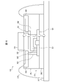
電流制御素子は、VCSEL及びスイッチング素子と直列に電気的に接続される、ことが好ましい。
スイッチング素子又は電流制御素子は、配線電極と、半田ボール、スタッドバンプ、又は、金属片を介して電気的に接続されている、ことが好ましい。
基板は金属製の第2電極として機能し、
VCSELは、表面に配置されるVCSEL第1端子、及び、裏面に配置されるVCSEL第2端子を有し、スイッチング素子は半導体装置内に形成され、
半導体装置は、第1電極及びカソードと接続される第1端子、カソードと接続される第2端子、及び、前記第2電極と接続される第3端子、を有することが好ましい。
第1端子は、第1電極に近接する第1側面に沿った上面の端部に配置され、
第2端子は、上面の中央部に配置され、
第3端子は、第2側面又は第3側面に沿った上面の端部に配置される、ことが好ましい。
監視回路と接続される監視回路用端子は、半導体装置の表面の第4面に沿った端部に配置される、ことが好ましい。
第4端子は、第3端子が配置された第2側面又は第3側面の他方に沿った上面の端部に配置され、
VCSELのカソードから半導体装置内に流入した電流は、第3端子及び第4端子により、半導体装置の左右に分かれて第2電極へ流れる、ことが好ましい。
Claims (13)
- 表面に配置されるVCSEL第1端子、及び、裏面に配置されるVCSEL第2端子を有するVCSELと、
第1側面、前記第1側面に直交する第2側面及び第3側面、前記第1側面と対向する第4側面、上面、及び下面を備える矩形の平板形状を有し且つ前記VCSELの下に配置され、前記VCSEL第2端子と電気的に接続されたVCSEL用のスイッチング素子が内部に形成される半導体装置と、
前記第1側面に沿って配置される金属製の第1電極と、
前記半導体装置の下に配置される金属製の第2電極と、を有し、
前記半導体装置は、
前記第1側面に沿う辺、前記第1側面に直交し且つ前記第1側面に沿う辺よりも短い一対の辺、及び前記第1側面に沿う辺に対向する辺により形成される矩形の平面形状を有し、前記上面の端部に配置され、且つ、第1電極及び前記VCSEL第1端子と接続される第1端子と、
前記上面の中央部に配置され、前記VCSEL第2端子と接続される第2端子と、
前記第2電極と接続される第3端子と、
を更に有する、ことを特徴とするVCSELモジュール。 - 前記半導体装置は、前記VCSELを流れる電流を制御する電流制御素子を有し、前記電流制御素子は、前記第2端子と前記スイッチング素子との間、又は、前記スイッチング素子と前記第3端子との間に接続される、請求項1に記載のVCSELモジュール。
- 前記第3端子は、前記第2側面又は前記第3側面に沿った前記上面の端部に配置される、請求項2に記載のVCSELモジュール。
- 前記第1電極と前記第1端子とは、複数のボンディングワイヤで接続されている、請求項3に記載のVCSELモジュール。
- 前記第2電極と前記第3端子とは、複数のボンディングワイヤで接続されている、請求項3又は4に記載のVCSELモジュール。
- 前記半導体装置は、前記VCSELの温度、前記VCSELを流れる電流、又は、前記VCSELから出射される光の光量を関する監視回路を有し、
前記監視回路と接続される監視回路用端子は、前記半導体装置の表面の前記第4側面に沿った端部に配置される、請求項3~5の何れか一項に記載のVCSELモジュール。 - 前記監視回路用端子と接続される第3電極を更に有する、請求項6に記載のVCSELモジュール。
- 前記第1電極及び前記第2電極の表面の一部、及び、前記第1端子及び第3端子の表面の一部を覆うように形成される樹脂製のフレームを更に有する、請求項2~7の何れか一項に記載のVCSELモジュール。
- 前記フレームは、前記VCSELが視認可能な開口部が形成される支持面を有する、請求項8に記載のVCSELモジュール。
- 前記支持面に支持され、前記VCSELから出射された光を透過する光学素子を更に有する、請求項9記載のVCSELモジュール。
- 前記フレームは、前記光学素子の位置決めをするために、前記支持面の上方で、且つ、当該フレームの外壁から内側に迫り出した凸部を有する、請求項10に記載のVCSELモジュール。
- 前記VCSELからの放熱を前記第2電極へ向けて伝達するための放熱経路が、前記半導体装置において、前記第2端子と前記半導体装置の前記下面との間に形成される、請求項3~11の何れか一項に記載のVCSELモジュール。
- 前記半導体装置は、前記第2電極と接続される第4端子、を有し、
前記第4端子は、前記第3端子が配置された前記第2側面又は前記第3側面の他方に沿った前記上面の端部に配置され、
前記VCSEL第2端子から前記半導体装置内に流入した電流は、前記第3端子及び前記第4端子により、前記半導体装置の左右に分かれて前記第2電極へ流れる、請求項3~12の何れか一項に記載のVCSELモジュール。
Priority Applications (1)
| Application Number | Priority Date | Filing Date | Title |
|---|---|---|---|
| JP2022161135A JP2022179619A (ja) | 2020-06-22 | 2022-10-05 | Vcselモジュール |
Applications Claiming Priority (5)
| Application Number | Priority Date | Filing Date | Title |
|---|---|---|---|
| JP2020107020 | 2020-06-22 | ||
| JP2020107020 | 2020-06-22 | ||
| JP2021052423 | 2021-03-25 | ||
| JP2021052423 | 2021-03-25 | ||
| PCT/JP2021/023664 WO2021261496A1 (ja) | 2020-06-22 | 2021-06-22 | Vcselモジュール |
Related Child Applications (1)
| Application Number | Title | Priority Date | Filing Date |
|---|---|---|---|
| JP2022161135A Division JP2022179619A (ja) | 2020-06-22 | 2022-10-05 | Vcselモジュール |
Publications (3)
| Publication Number | Publication Date |
|---|---|
| JPWO2021261496A1 JPWO2021261496A1 (ja) | 2021-12-30 |
| JPWO2021261496A5 JPWO2021261496A5 (ja) | 2022-06-10 |
| JP7155455B2 true JP7155455B2 (ja) | 2022-10-18 |
Family
ID=79281242
Family Applications (2)
| Application Number | Title | Priority Date | Filing Date |
|---|---|---|---|
| JP2022516276A Active JP7155455B2 (ja) | 2020-06-22 | 2021-06-22 | Vcselモジュール |
| JP2022161135A Pending JP2022179619A (ja) | 2020-06-22 | 2022-10-05 | Vcselモジュール |
Family Applications After (1)
| Application Number | Title | Priority Date | Filing Date |
|---|---|---|---|
| JP2022161135A Pending JP2022179619A (ja) | 2020-06-22 | 2022-10-05 | Vcselモジュール |
Country Status (3)
| Country | Link |
|---|---|
| JP (2) | JP7155455B2 (ja) |
| CN (1) | CN115943533A (ja) |
| WO (1) | WO2021261496A1 (ja) |
Citations (10)
| Publication number | Priority date | Publication date | Assignee | Title |
|---|---|---|---|---|
| JP2010531546A (ja) | 2007-06-27 | 2010-09-24 | コーニンクレッカ フィリップス エレクトロニクス エヌ ヴィ | 光センサ・モジュール及びその製造方法 |
| JP2012037276A (ja) | 2010-08-04 | 2012-02-23 | Sharp Corp | 光学式測距装置 |
| WO2014017256A1 (ja) | 2012-07-24 | 2014-01-30 | シャープ株式会社 | 光学式測距装置および電子機器 |
| WO2018100082A1 (en) | 2016-11-30 | 2018-06-07 | Sony Semiconductor Solutions Corporation | Apparatus and method |
| US20180278011A1 (en) | 2017-03-23 | 2018-09-27 | Infineon Technologies Ag | Laser diode module |
| JP2019158693A (ja) | 2018-03-15 | 2019-09-19 | 株式会社リコー | 受光装置、物体検出装置、距離測定装置、移動体装置、ノイズ計測方法、物体検出方法及び距離測定方法 |
| US20200006271A1 (en) | 2018-07-02 | 2020-01-02 | Taiwan Semiconductor Manufacturing Co., Ltd. | Structures for bonding a group iii-v device to a substrate |
| WO2020044817A1 (ja) | 2018-08-31 | 2020-03-05 | ソニーセミコンダクタソリューションズ株式会社 | 光源装置、検出方法、センシングモジュール |
| WO2020054257A1 (ja) | 2018-09-11 | 2020-03-19 | ソニーセミコンダクタソリューションズ株式会社 | 光源装置、センシングモジュール |
| US20200185875A1 (en) | 2018-12-06 | 2020-06-11 | Finisar Corporation | Optoelectronic assembly |
Family Cites Families (2)
| Publication number | Priority date | Publication date | Assignee | Title |
|---|---|---|---|---|
| JPH06237016A (ja) * | 1993-02-09 | 1994-08-23 | Matsushita Electric Ind Co Ltd | 光ファイバモジュールおよびその製造方法 |
| JP2021114556A (ja) * | 2020-01-20 | 2021-08-05 | ソニーセミコンダクタソリューションズ株式会社 | 発光装置およびその製造方法 |
-
2021
- 2021-06-22 WO PCT/JP2021/023664 patent/WO2021261496A1/ja active Application Filing
- 2021-06-22 JP JP2022516276A patent/JP7155455B2/ja active Active
- 2021-06-22 CN CN202180044387.9A patent/CN115943533A/zh active Pending
-
2022
- 2022-10-05 JP JP2022161135A patent/JP2022179619A/ja active Pending
Patent Citations (10)
| Publication number | Priority date | Publication date | Assignee | Title |
|---|---|---|---|---|
| JP2010531546A (ja) | 2007-06-27 | 2010-09-24 | コーニンクレッカ フィリップス エレクトロニクス エヌ ヴィ | 光センサ・モジュール及びその製造方法 |
| JP2012037276A (ja) | 2010-08-04 | 2012-02-23 | Sharp Corp | 光学式測距装置 |
| WO2014017256A1 (ja) | 2012-07-24 | 2014-01-30 | シャープ株式会社 | 光学式測距装置および電子機器 |
| WO2018100082A1 (en) | 2016-11-30 | 2018-06-07 | Sony Semiconductor Solutions Corporation | Apparatus and method |
| US20180278011A1 (en) | 2017-03-23 | 2018-09-27 | Infineon Technologies Ag | Laser diode module |
| JP2019158693A (ja) | 2018-03-15 | 2019-09-19 | 株式会社リコー | 受光装置、物体検出装置、距離測定装置、移動体装置、ノイズ計測方法、物体検出方法及び距離測定方法 |
| US20200006271A1 (en) | 2018-07-02 | 2020-01-02 | Taiwan Semiconductor Manufacturing Co., Ltd. | Structures for bonding a group iii-v device to a substrate |
| WO2020044817A1 (ja) | 2018-08-31 | 2020-03-05 | ソニーセミコンダクタソリューションズ株式会社 | 光源装置、検出方法、センシングモジュール |
| WO2020054257A1 (ja) | 2018-09-11 | 2020-03-19 | ソニーセミコンダクタソリューションズ株式会社 | 光源装置、センシングモジュール |
| US20200185875A1 (en) | 2018-12-06 | 2020-06-11 | Finisar Corporation | Optoelectronic assembly |
Also Published As
| Publication number | Publication date |
|---|---|
| JPWO2021261496A1 (ja) | 2021-12-30 |
| CN115943533A (zh) | 2023-04-07 |
| JP2022179619A (ja) | 2022-12-02 |
| WO2021261496A1 (ja) | 2021-12-30 |
Similar Documents
| Publication | Publication Date | Title |
|---|---|---|
| US10490722B2 (en) | Light emitting package having a guiding member guiding an optical member | |
| US7586125B2 (en) | Light emitting diode package structure and fabricating method thereof | |
| US7855396B2 (en) | Light emitting diode package structure | |
| JP2003008083A (ja) | 多数チップ半導体ledアセンブリ | |
| JP7155455B2 (ja) | Vcselモジュール | |
| KR101259876B1 (ko) | 열전 소자를 갖는 엘이디 패키지 및 이의 제조 방법 | |
| JP2005294292A (ja) | 発光装置及び発光装置の製造方法 | |
| JP2022167697A (ja) | 発光装置 | |
| JP2022168626A (ja) | 発光装置 | |
| JP2022164487A (ja) | 発光装置 |
Legal Events
| Date | Code | Title | Description |
|---|---|---|---|
| A529 | Written submission of copy of amendment under article 34 pct |
Free format text: JAPANESE INTERMEDIATE CODE: A5211 Effective date: 20220311 |
|
| A621 | Written request for application examination |
Free format text: JAPANESE INTERMEDIATE CODE: A621 Effective date: 20220311 |
|
| A871 | Explanation of circumstances concerning accelerated examination |
Free format text: JAPANESE INTERMEDIATE CODE: A871 Effective date: 20220311 |
|
| A131 | Notification of reasons for refusal |
Free format text: JAPANESE INTERMEDIATE CODE: A131 Effective date: 20220705 |
|
| A521 | Request for written amendment filed |
Free format text: JAPANESE INTERMEDIATE CODE: A523 Effective date: 20220713 |
|
| TRDD | Decision of grant or rejection written | ||
| A01 | Written decision to grant a patent or to grant a registration (utility model) |
Free format text: JAPANESE INTERMEDIATE CODE: A01 Effective date: 20220906 |
|
| A61 | First payment of annual fees (during grant procedure) |
Free format text: JAPANESE INTERMEDIATE CODE: A61 Effective date: 20221005 |
|
| R150 | Certificate of patent or registration of utility model |
Ref document number: 7155455 Country of ref document: JP Free format text: JAPANESE INTERMEDIATE CODE: R150 |