JP7155007B2 - フォトニック集積回路におけるレーザアライメントのための技術 - Google Patents
フォトニック集積回路におけるレーザアライメントのための技術 Download PDFInfo
- Publication number
- JP7155007B2 JP7155007B2 JP2018544056A JP2018544056A JP7155007B2 JP 7155007 B2 JP7155007 B2 JP 7155007B2 JP 2018544056 A JP2018544056 A JP 2018544056A JP 2018544056 A JP2018544056 A JP 2018544056A JP 7155007 B2 JP7155007 B2 JP 7155007B2
- Authority
- JP
- Japan
- Prior art keywords
- laser
- substrate
- pic
- semiconductor laser
- mating surface
- Prior art date
- Legal status (The legal status is an assumption and is not a legal conclusion. Google has not performed a legal analysis and makes no representation as to the accuracy of the status listed.)
- Active
Links
Images


Classifications
-
- H—ELECTRICITY
- H01—ELECTRIC ELEMENTS
- H01S—DEVICES USING THE PROCESS OF LIGHT AMPLIFICATION BY STIMULATED EMISSION OF RADIATION [LASER] TO AMPLIFY OR GENERATE LIGHT; DEVICES USING STIMULATED EMISSION OF ELECTROMAGNETIC RADIATION IN WAVE RANGES OTHER THAN OPTICAL
- H01S5/00—Semiconductor lasers
- H01S5/02—Structural details or components not essential to laser action
- H01S5/022—Mountings; Housings
- H01S5/0233—Mounting configuration of laser chips
-
- G—PHYSICS
- G02—OPTICS
- G02B—OPTICAL ELEMENTS, SYSTEMS OR APPARATUS
- G02B6/00—Light guides; Structural details of arrangements comprising light guides and other optical elements, e.g. couplings
- G02B6/24—Coupling light guides
- G02B6/42—Coupling light guides with opto-electronic elements
-
- G—PHYSICS
- G02—OPTICS
- G02B—OPTICAL ELEMENTS, SYSTEMS OR APPARATUS
- G02B6/00—Light guides; Structural details of arrangements comprising light guides and other optical elements, e.g. couplings
- G02B6/24—Coupling light guides
- G02B6/42—Coupling light guides with opto-electronic elements
- G02B6/4201—Packages, e.g. shape, construction, internal or external details
- G02B6/4219—Mechanical fixtures for holding or positioning the elements relative to each other in the couplings; Alignment methods for the elements, e.g. measuring or observing methods especially used therefor
- G02B6/4228—Passive alignment, i.e. without a detection of the degree of coupling or the position of the elements
- G02B6/423—Passive alignment, i.e. without a detection of the degree of coupling or the position of the elements using guiding surfaces for the alignment
-
- G—PHYSICS
- G02—OPTICS
- G02B—OPTICAL ELEMENTS, SYSTEMS OR APPARATUS
- G02B6/00—Light guides; Structural details of arrangements comprising light guides and other optical elements, e.g. couplings
- G02B6/24—Coupling light guides
- G02B6/42—Coupling light guides with opto-electronic elements
- G02B6/4201—Packages, e.g. shape, construction, internal or external details
- G02B6/4219—Mechanical fixtures for holding or positioning the elements relative to each other in the couplings; Alignment methods for the elements, e.g. measuring or observing methods especially used therefor
- G02B6/4228—Passive alignment, i.e. without a detection of the degree of coupling or the position of the elements
- G02B6/4232—Passive alignment, i.e. without a detection of the degree of coupling or the position of the elements using the surface tension of fluid solder to align the elements, e.g. solder bump techniques
-
- G—PHYSICS
- G02—OPTICS
- G02B—OPTICAL ELEMENTS, SYSTEMS OR APPARATUS
- G02B6/00—Light guides; Structural details of arrangements comprising light guides and other optical elements, e.g. couplings
- G02B6/24—Coupling light guides
- G02B6/42—Coupling light guides with opto-electronic elements
- G02B6/4201—Packages, e.g. shape, construction, internal or external details
- G02B6/4219—Mechanical fixtures for holding or positioning the elements relative to each other in the couplings; Alignment methods for the elements, e.g. measuring or observing methods especially used therefor
- G02B6/4236—Fixing or mounting methods of the aligned elements
- G02B6/4238—Soldering
-
- H—ELECTRICITY
- H01—ELECTRIC ELEMENTS
- H01S—DEVICES USING THE PROCESS OF LIGHT AMPLIFICATION BY STIMULATED EMISSION OF RADIATION [LASER] TO AMPLIFY OR GENERATE LIGHT; DEVICES USING STIMULATED EMISSION OF ELECTROMAGNETIC RADIATION IN WAVE RANGES OTHER THAN OPTICAL
- H01S5/00—Semiconductor lasers
- H01S5/02—Structural details or components not essential to laser action
- H01S5/022—Mountings; Housings
- H01S5/023—Mount members, e.g. sub-mount members
- H01S5/02325—Mechanically integrated components on mount members or optical micro-benches
- H01S5/02326—Arrangements for relative positioning of laser diodes and optical components, e.g. grooves in the mount to fix optical fibres or lenses
-
- H—ELECTRICITY
- H01—ELECTRIC ELEMENTS
- H01S—DEVICES USING THE PROCESS OF LIGHT AMPLIFICATION BY STIMULATED EMISSION OF RADIATION [LASER] TO AMPLIFY OR GENERATE LIGHT; DEVICES USING STIMULATED EMISSION OF ELECTROMAGNETIC RADIATION IN WAVE RANGES OTHER THAN OPTICAL
- H01S5/00—Semiconductor lasers
- H01S5/02—Structural details or components not essential to laser action
- H01S5/022—Mountings; Housings
- H01S5/0233—Mounting configuration of laser chips
- H01S5/02345—Wire-bonding
-
- H—ELECTRICITY
- H01—ELECTRIC ELEMENTS
- H01S—DEVICES USING THE PROCESS OF LIGHT AMPLIFICATION BY STIMULATED EMISSION OF RADIATION [LASER] TO AMPLIFY OR GENERATE LIGHT; DEVICES USING STIMULATED EMISSION OF ELECTROMAGNETIC RADIATION IN WAVE RANGES OTHER THAN OPTICAL
- H01S5/00—Semiconductor lasers
- H01S5/02—Structural details or components not essential to laser action
- H01S5/022—Mountings; Housings
- H01S5/0235—Method for mounting laser chips
- H01S5/02355—Fixing laser chips on mounts
- H01S5/0237—Fixing laser chips on mounts by soldering
-
- H—ELECTRICITY
- H01—ELECTRIC ELEMENTS
- H01S—DEVICES USING THE PROCESS OF LIGHT AMPLIFICATION BY STIMULATED EMISSION OF RADIATION [LASER] TO AMPLIFY OR GENERATE LIGHT; DEVICES USING STIMULATED EMISSION OF ELECTROMAGNETIC RADIATION IN WAVE RANGES OTHER THAN OPTICAL
- H01S5/00—Semiconductor lasers
- H01S5/02—Structural details or components not essential to laser action
- H01S5/022—Mountings; Housings
- H01S5/0235—Method for mounting laser chips
- H01S5/02375—Positioning of the laser chips
-
- H—ELECTRICITY
- H01—ELECTRIC ELEMENTS
- H01S—DEVICES USING THE PROCESS OF LIGHT AMPLIFICATION BY STIMULATED EMISSION OF RADIATION [LASER] TO AMPLIFY OR GENERATE LIGHT; DEVICES USING STIMULATED EMISSION OF ELECTROMAGNETIC RADIATION IN WAVE RANGES OTHER THAN OPTICAL
- H01S5/00—Semiconductor lasers
- H01S5/02—Structural details or components not essential to laser action
- H01S5/026—Monolithically integrated components, e.g. waveguides, monitoring photo-detectors, drivers
-
- H—ELECTRICITY
- H01—ELECTRIC ELEMENTS
- H01S—DEVICES USING THE PROCESS OF LIGHT AMPLIFICATION BY STIMULATED EMISSION OF RADIATION [LASER] TO AMPLIFY OR GENERATE LIGHT; DEVICES USING STIMULATED EMISSION OF ELECTROMAGNETIC RADIATION IN WAVE RANGES OTHER THAN OPTICAL
- H01S5/00—Semiconductor lasers
- H01S5/10—Construction or shape of the optical resonator, e.g. extended or external cavity, coupled cavities, bent-guide, varying width, thickness or composition of the active region
- H01S5/1082—Construction or shape of the optical resonator, e.g. extended or external cavity, coupled cavities, bent-guide, varying width, thickness or composition of the active region with a special facet structure, e.g. structured, non planar, oblique
- H01S5/1085—Oblique facets
-
- H—ELECTRICITY
- H01—ELECTRIC ELEMENTS
- H01S—DEVICES USING THE PROCESS OF LIGHT AMPLIFICATION BY STIMULATED EMISSION OF RADIATION [LASER] TO AMPLIFY OR GENERATE LIGHT; DEVICES USING STIMULATED EMISSION OF ELECTROMAGNETIC RADIATION IN WAVE RANGES OTHER THAN OPTICAL
- H01S5/00—Semiconductor lasers
- H01S5/005—Optical components external to the laser cavity, specially adapted therefor, e.g. for homogenisation or merging of the beams or for manipulating laser pulses, e.g. pulse shaping
-
- H—ELECTRICITY
- H01—ELECTRIC ELEMENTS
- H01S—DEVICES USING THE PROCESS OF LIGHT AMPLIFICATION BY STIMULATED EMISSION OF RADIATION [LASER] TO AMPLIFY OR GENERATE LIGHT; DEVICES USING STIMULATED EMISSION OF ELECTROMAGNETIC RADIATION IN WAVE RANGES OTHER THAN OPTICAL
- H01S5/00—Semiconductor lasers
- H01S5/02—Structural details or components not essential to laser action
- H01S5/022—Mountings; Housings
- H01S5/0233—Mounting configuration of laser chips
- H01S5/0234—Up-side down mountings, e.g. Flip-chip, epi-side down mountings or junction down mountings
-
- H—ELECTRICITY
- H01—ELECTRIC ELEMENTS
- H01S—DEVICES USING THE PROCESS OF LIGHT AMPLIFICATION BY STIMULATED EMISSION OF RADIATION [LASER] TO AMPLIFY OR GENERATE LIGHT; DEVICES USING STIMULATED EMISSION OF ELECTROMAGNETIC RADIATION IN WAVE RANGES OTHER THAN OPTICAL
- H01S5/00—Semiconductor lasers
- H01S5/10—Construction or shape of the optical resonator, e.g. extended or external cavity, coupled cavities, bent-guide, varying width, thickness or composition of the active region
- H01S5/1082—Construction or shape of the optical resonator, e.g. extended or external cavity, coupled cavities, bent-guide, varying width, thickness or composition of the active region with a special facet structure, e.g. structured, non planar, oblique
-
- H—ELECTRICITY
- H01—ELECTRIC ELEMENTS
- H01S—DEVICES USING THE PROCESS OF LIGHT AMPLIFICATION BY STIMULATED EMISSION OF RADIATION [LASER] TO AMPLIFY OR GENERATE LIGHT; DEVICES USING STIMULATED EMISSION OF ELECTROMAGNETIC RADIATION IN WAVE RANGES OTHER THAN OPTICAL
- H01S5/00—Semiconductor lasers
- H01S5/30—Structure or shape of the active region; Materials used for the active region
- H01S5/32—Structure or shape of the active region; Materials used for the active region comprising PN junctions, e.g. hetero- or double- heterostructures
- H01S5/3211—Structure or shape of the active region; Materials used for the active region comprising PN junctions, e.g. hetero- or double- heterostructures characterised by special cladding layers, e.g. details on band-discontinuities
Landscapes
- Physics & Mathematics (AREA)
- General Physics & Mathematics (AREA)
- Optics & Photonics (AREA)
- Condensed Matter Physics & Semiconductors (AREA)
- Electromagnetism (AREA)
- Semiconductor Lasers (AREA)
- Optical Couplings Of Light Guides (AREA)
- Optical Integrated Circuits (AREA)
Description
本願は、2016年2月19日に出願された米国特許仮出願第62/297,735号の優先権主張出願であり、この米国特許仮出願を参照により引用し、この記載内容全体を本明細書の一部とする。
Claims (23)
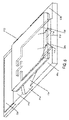
- フォトニック集積回路(PIC)であって、
テーパ付きレーザ合わせ面と、前記テーパ付きレーザ合わせ面の前縁から後退したレーザファセットと、を備えた半導体レーザと、
テーパ付き基板合わせ面と導波路を備えた基板とを有し、
前記半導体レーザが前記基板にアライメントされるときに、前記テーパ付きレーザ合わせ面の前記前縁は、前記テーパ付き基板合わせ面に接触して、前記半導体レーザの前記レーザファセットを出るレーザビームと前記導波路との間のアライメント誤差を減少させるよう構成されている、PIC。 - 前記テーパ付きレーザ合わせ面の形状および前記テーパ付き基板合わせ面の形状は、外力が前記半導体レーザに加えられると、前記半導体レーザを前記基板にアライメントするよう構成されている、請求項1記載のPIC。
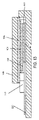
- 前記半導体レーザが前記基板にアライメントされると、前記基板の後壁は、前記半導体レーザの後側部分に接触するよう構成され、前記基板の側壁は、前記半導体レーザの側面に接触するよう構成されている、請求項2記載のPIC。
- 前記半導体レーザの前記側面の一部分は、前記半導体レーザが前記基板にアライメントされると、前記基板の隙間部分の上方に配置されるよう構成されている、請求項3記載のPIC。
- 前記外力は、前記半導体レーザから前記基板に向かう方向に加えられる、請求項2記載のPIC。
- 前記テーパ付きレーザ合わせ面の形状は、三角形または台形である、請求項1記載のPIC。
- 前記テーパ付き基板合わせ面の形状は、三角形、または台形である、請求項1記載のPIC。
- 前記テーパ付きレーザ合わせ面の第1のエッジは、前記テーパ付き基板合わせ面に接触し、前記テーパ付きレーザ合わせ面の第2のエッジは、前記テーパ付き基板合わせ面に接触しない、請求項1記載のPIC。
- 前記テーパ付き基板合わせ面は、湾曲したエッジを有し、前記湾曲したエッジは、前記基板との前記半導体レーザのアライメント中、前記半導体レーザに加えられる外力を分散させるよう構成されている、請求項1記載のPIC。
- 前記導波路は、前記レーザファセットを出た前記レーザビームを受け取るよう構成されている、請求項1記載のPIC。
- 前記レーザファセットは、レーザ光が前記レーザファセットを出る方向に対して角度が付けられ、前記導波路の前縁は、前記レーザファセットと同様に同じ方向に対して角度が付けられ、前記レーザファセットの前記角度および前記導波路の前記前縁の前記角度は、前記導波路から前記レーザファセットへの前記レーザビームの後方反射を減少させるよう構成されている、請求項10記載のPIC。
- 前記レーザファセットと前記導波路の前記前縁は、同一方向に角度が付けられている、請求項11記載のPIC。
- 前記レーザファセットは、レーザ光が前記レーザファセットを出る方向に対して垂直方向または水平方向に角度が付けられている、請求項11記載のPIC。
- 前記半導体レーザは、前記基板との電気接続部を形成するよう構成された接触面を有し、
前記基板は、前記半導体レーザを受け入れるよう構成されたランディング領域を更に有し、前記ランディング領域は、
前記テーパ付き基板合わせ面と、
前記半導体レーザの前記接触面に電気的に結合するよう構成された接触パッドとを有する、請求項1記載のPIC。 - はんだが前記接触パッドと前記半導体レーザの前記接触面との間に施されている、請求項14記載のPIC。
- 前記ランディング領域は、
前記接触パッドに配置されたはんだ層と、
前記接触パッドに配置された前記はんだ層から前記はんだを受け入れるよう構成されたランオフ領域とを更に有する、請求項14記載のPIC。 - 前記ランオフ領域は、前記はんだ層からのはんだを前記接触パッドから引き離すことによってはんだを受け入れるよう構成されている、請求項16記載のPIC。
- 前記ランオフ領域は、前記接触パッドに対して垂直に角度が付けられている、請求項17記載のPIC。
- フォトニック集積回路(PIC)を作製する方法であって、前記方法は、
半導体レーザを基板上に配置するステップを含み、前記半導体レーザは、テーパ付きレーザ合わせ面と、前記テーパ付きレーザ合わせ面の前縁から後退したレーザファセットと、を有し、前記基板は、テーパ付き基板合わせ面と導波路を有し、
前記テーパ付きレーザ合わせ面の前記前縁と前記テーパ付き基板合わせ面との接触を用いて、前記半導体レーザの前記レーザファセットを出るレーザビームと前記導波路との間のアライメント誤差を減少させて、前記半導体レーザを前記基板にアライメントするステップを含む、方法。 - 外力を前記半導体レーザから前記基板に向かう方向で前記半導体レーザに加えるステップを更に含む、請求項19記載の方法。
- 前記テーパ付き基板合わせ面の湾曲したエッジを用いて前記外力を分散させるステップを更に含む、請求項20記載の方法。
- 前記半導体レーザを前記基板上に配置する前記ステップに先立って、はんだを前記半導体レーザの接触面に付着させるステップを更に含み、前記半導体レーザを前記基板上に配置する前記ステップは、前記半導体レーザの前記接触面を前記基板の接触パッドに取り付けるステップを含み、前記はんだは、前記接触面と前記接触パッドの間に配置される、請求項19記載の方法。
- 前記はんだの表面張力が前記テーパ付きレーザ合わせ面を引いて該テーパ付きレーザ合わせ面を前記テーパ付き基板合わせ面に取り付ける、請求項22記載の方法。
Priority Applications (1)
| Application Number | Priority Date | Filing Date | Title |
|---|---|---|---|
| JP2022160918A JP2022189842A (ja) | 2016-02-19 | 2022-10-05 | フォトニック集積回路におけるレーザアライメントのための技術 |
Applications Claiming Priority (3)
| Application Number | Priority Date | Filing Date | Title |
|---|---|---|---|
| US201662297735P | 2016-02-19 | 2016-02-19 | |
| US62/297,735 | 2016-02-19 | ||
| PCT/US2017/018481 WO2017143264A1 (en) | 2016-02-19 | 2017-02-17 | Techniques for laser alignment in photonic integrated circuits |
Related Child Applications (1)
| Application Number | Title | Priority Date | Filing Date |
|---|---|---|---|
| JP2022160918A Division JP2022189842A (ja) | 2016-02-19 | 2022-10-05 | フォトニック集積回路におけるレーザアライメントのための技術 |
Publications (2)
| Publication Number | Publication Date |
|---|---|
| JP2019509635A JP2019509635A (ja) | 2019-04-04 |
| JP7155007B2 true JP7155007B2 (ja) | 2022-10-18 |
Family
ID=59626373
Family Applications (2)
| Application Number | Title | Priority Date | Filing Date |
|---|---|---|---|
| JP2018544056A Active JP7155007B2 (ja) | 2016-02-19 | 2017-02-17 | フォトニック集積回路におけるレーザアライメントのための技術 |
| JP2022160918A Pending JP2022189842A (ja) | 2016-02-19 | 2022-10-05 | フォトニック集積回路におけるレーザアライメントのための技術 |
Family Applications After (1)
| Application Number | Title | Priority Date | Filing Date |
|---|---|---|---|
| JP2022160918A Pending JP2022189842A (ja) | 2016-02-19 | 2022-10-05 | フォトニック集積回路におけるレーザアライメントのための技術 |
Country Status (8)
| Country | Link |
|---|---|
| US (3) | US10027087B2 (ja) |
| EP (3) | EP3447556B1 (ja) |
| JP (2) | JP7155007B2 (ja) |
| KR (1) | KR102545749B1 (ja) |
| CN (2) | CN109075525A (ja) |
| CA (1) | CA3014585C (ja) |
| IL (1) | IL261072B (ja) |
| WO (1) | WO2017143264A1 (ja) |
Families Citing this family (7)
| Publication number | Priority date | Publication date | Assignee | Title |
|---|---|---|---|---|
| WO2020106974A1 (en) * | 2018-11-21 | 2020-05-28 | Skorpios Technologies, Inc. | Etched facet in a multi quantum well structure |
| FR3091932B1 (fr) * | 2019-01-22 | 2021-02-12 | St Microelectronics Crolles 2 Sas | Système photonique et son procédé de fabrication |
| CN110764196B (zh) * | 2019-09-09 | 2020-12-08 | 浙江大学 | 用于光纤阵列与平面光波导耦合的无导销可插拔对准结构 |
| US11888286B2 (en) * | 2020-10-21 | 2024-01-30 | Marvell Asia Pte Ltd | Laser chip for flip-chip bonding on silicon photonics chips |
| TWI786599B (zh) * | 2021-04-15 | 2022-12-11 | 國立高雄科技大學 | 角型反射的高速光二極體結構 |
| WO2023174669A1 (en) * | 2022-03-15 | 2023-09-21 | Ams-Osram International Gmbh | Laser diode component, laser diode apparatus and method for producing a laser diode component |
| CN116338366B (zh) * | 2023-05-29 | 2023-09-29 | 中久光电产业有限公司 | 半导体激光器vbg耦合过程检测设备 |
Citations (6)
| Publication number | Priority date | Publication date | Assignee | Title |
|---|---|---|---|---|
| JP2000105322A (ja) | 1998-09-29 | 2000-04-11 | Nippon Telegr & Teleph Corp <Ntt> | 光部品用実装基板および光部品用実装基板の製造方法 |
| JP2000510256A (ja) | 1996-05-16 | 2000-08-08 | ブッカム テクノロジー リミテッド | 光学部材および光導波路の組立体 |
| JP2002072027A (ja) | 2000-09-01 | 2002-03-12 | Opnext Japan Inc | 光モジュール、光伝送装置及びその製造方法 |
| US20020119588A1 (en) | 1999-03-29 | 2002-08-29 | Bowen Terry Patrick | Method for fabricating fiducials for passive alignment of opto-electronic devices |
| WO2003034115A2 (en) | 2001-10-17 | 2003-04-24 | Bookham Technology Plc | Coupling a semiconducter laser to an optical waveguide |
| JP2015519008A (ja) | 2012-05-08 | 2015-07-06 | ビノプティクス・コーポレイションBinoptics Corporation | ビーム形状の改良を伴うレーザ |
Family Cites Families (22)
| Publication number | Priority date | Publication date | Assignee | Title |
|---|---|---|---|---|
| JP2813780B2 (ja) * | 1990-01-08 | 1998-10-22 | 日本電信電話株式会社 | ハイブリッド型光集積回路 |
| US5023881A (en) * | 1990-06-19 | 1991-06-11 | At&T Bell Laboratories | Photonics module and alignment method |
| JP2762792B2 (ja) * | 1991-08-30 | 1998-06-04 | 日本電気株式会社 | 光半導体装置 |
| WO1993015424A1 (en) * | 1992-01-28 | 1993-08-05 | British Telecommunications Public Limited Company | Alignment of integrated optical components |
| JP2869279B2 (ja) * | 1992-09-16 | 1999-03-10 | 三菱電機株式会社 | 半導体レーザダイオード及びその製造方法並びに半導体レーザダイオードアレイ |
| JP3117107B2 (ja) * | 1993-08-03 | 2000-12-11 | シャープ株式会社 | 光集積回路素子の組立構造 |
| US5376582A (en) * | 1993-10-15 | 1994-12-27 | International Business Machines Corporation | Planar, topology-free, single-mode, high-power semiconductor quantum-well laser with non-absorbing mirrors and current confinement |
| JP3658426B2 (ja) * | 1995-01-23 | 2005-06-08 | 株式会社日立製作所 | 光半導体装置 |
| JP3184440B2 (ja) * | 1995-02-10 | 2001-07-09 | 株式会社リコー | 半導体発光装置 |
| US5838703A (en) * | 1996-09-30 | 1998-11-17 | Motorola, Inc. | Semiconductor laser package with power monitoring system and optical element |
| US6327289B1 (en) * | 1997-09-02 | 2001-12-04 | Matsushita Electric Industrial Co., Ltd. | Wavelength-variable semiconductor laser, optical integrated device utilizing the same, and production method thereof |
| JPH11191643A (ja) * | 1997-12-25 | 1999-07-13 | Kyocera Corp | チップキャリア及びこれを用いた光素子モジュール |
| PL365959A1 (en) * | 1999-07-16 | 2005-01-24 | Hybrid Micro Technologies Aps | Hybrid integration of active and passive optical components on an si-board |
| JP4198867B2 (ja) | 2000-06-23 | 2008-12-17 | 株式会社東芝 | アンテナ装置 |
| WO2003038497A1 (en) * | 2001-10-30 | 2003-05-08 | Xponent Photonics, Inc. | Optical junction apparatus and methods employing optical power transverse-transfer |
| US6993053B2 (en) * | 2002-04-03 | 2006-01-31 | The Australian National University | Thin clad diode laser |
| KR100975521B1 (ko) * | 2003-10-04 | 2010-08-12 | 삼성전자주식회사 | 발광 소자 조립체 |
| JP3987500B2 (ja) * | 2004-02-17 | 2007-10-10 | 浜松ホトニクス株式会社 | 光配線基板および光配線基板の製造方法 |
| KR100637929B1 (ko) * | 2004-11-03 | 2006-10-24 | 한국전자통신연구원 | 하이브리드형 광소자 |
| JP5156502B2 (ja) * | 2007-06-26 | 2013-03-06 | パナソニック株式会社 | 光モジュール |
| US8168939B2 (en) | 2008-07-09 | 2012-05-01 | Luxtera, Inc. | Method and system for a light source assembly supporting direct coupling to an integrated circuit |
| US10176833B1 (en) * | 2016-01-22 | 2019-01-08 | Seagate Technology Llc | Horizontal cavity surface emitting laser integration features for heat assisted magnetic recording |
-
2017
- 2017-02-17 EP EP18194958.7A patent/EP3447556B1/en active Active
- 2017-02-17 EP EP20163531.5A patent/EP3691060B1/en active Active
- 2017-02-17 CN CN201780020561.XA patent/CN109075525A/zh active Pending
- 2017-02-17 CA CA3014585A patent/CA3014585C/en active Active
- 2017-02-17 US US15/436,474 patent/US10027087B2/en active Active
- 2017-02-17 KR KR1020187026725A patent/KR102545749B1/ko active IP Right Grant
- 2017-02-17 WO PCT/US2017/018481 patent/WO2017143264A1/en active Application Filing
- 2017-02-17 EP EP17753975.6A patent/EP3403303B1/en active Active
- 2017-02-17 CN CN202010111899.XA patent/CN111509555B/zh active Active
- 2017-02-17 JP JP2018544056A patent/JP7155007B2/ja active Active
-
2018
- 2018-07-16 US US16/036,454 patent/US11658459B2/en active Active
- 2018-08-09 IL IL261072A patent/IL261072B/en unknown
-
2022
- 2022-10-05 JP JP2022160918A patent/JP2022189842A/ja active Pending
-
2023
- 2023-04-26 US US18/307,362 patent/US20230261432A1/en active Pending
Patent Citations (6)
| Publication number | Priority date | Publication date | Assignee | Title |
|---|---|---|---|---|
| JP2000510256A (ja) | 1996-05-16 | 2000-08-08 | ブッカム テクノロジー リミテッド | 光学部材および光導波路の組立体 |
| JP2000105322A (ja) | 1998-09-29 | 2000-04-11 | Nippon Telegr & Teleph Corp <Ntt> | 光部品用実装基板および光部品用実装基板の製造方法 |
| US20020119588A1 (en) | 1999-03-29 | 2002-08-29 | Bowen Terry Patrick | Method for fabricating fiducials for passive alignment of opto-electronic devices |
| JP2002072027A (ja) | 2000-09-01 | 2002-03-12 | Opnext Japan Inc | 光モジュール、光伝送装置及びその製造方法 |
| WO2003034115A2 (en) | 2001-10-17 | 2003-04-24 | Bookham Technology Plc | Coupling a semiconducter laser to an optical waveguide |
| JP2015519008A (ja) | 2012-05-08 | 2015-07-06 | ビノプティクス・コーポレイションBinoptics Corporation | ビーム形状の改良を伴うレーザ |
Non-Patent Citations (1)
| Title |
|---|
| Etienne E. L. Friedrich, et al.,"Hybrid Integration of Semiconductor Lasers with Si-Based Single-Mode Ridge Waveguides",Journal of Lightwave Technology,1992年05月,Vol.10,No.3,p.336-340 |
Also Published As
| Publication number | Publication date |
|---|---|
| IL261072B (en) | 2022-03-01 |
| EP3691060B1 (en) | 2021-09-08 |
| CN111509555A (zh) | 2020-08-07 |
| EP3691060A1 (en) | 2020-08-05 |
| US20180342851A1 (en) | 2018-11-29 |
| US20230261432A1 (en) | 2023-08-17 |
| JP2019509635A (ja) | 2019-04-04 |
| KR20180115289A (ko) | 2018-10-22 |
| EP3403303B1 (en) | 2020-04-22 |
| IL261072A (en) | 2018-10-31 |
| US11658459B2 (en) | 2023-05-23 |
| CN109075525A (zh) | 2018-12-21 |
| EP3447556A2 (en) | 2019-02-27 |
| JP2022189842A (ja) | 2022-12-22 |
| CA3014585A1 (en) | 2017-08-24 |
| CA3014585C (en) | 2024-03-19 |
| EP3403303A1 (en) | 2018-11-21 |
| WO2017143264A1 (en) | 2017-08-24 |
| EP3403303A4 (en) | 2019-04-03 |
| US20170244216A1 (en) | 2017-08-24 |
| US10027087B2 (en) | 2018-07-17 |
| EP3447556A3 (en) | 2019-03-27 |
| KR102545749B1 (ko) | 2023-06-21 |
| EP3447556B1 (en) | 2020-04-29 |
| CN111509555B (zh) | 2024-02-27 |
Similar Documents
| Publication | Publication Date | Title |
|---|---|---|
| JP7155007B2 (ja) | フォトニック集積回路におけるレーザアライメントのための技術 | |
| US9692202B2 (en) | Lasers with beam shape and beam direction modification | |
| JP3117107B2 (ja) | 光集積回路素子の組立構造 | |
| US7656922B2 (en) | Multi-level integrated photonic devices | |
| US8563342B2 (en) | Method of making semiconductor optical integrated device by alternately arranging spacers with integrated device arrays | |
| JP2008113041A (ja) | 導波管 | |
| JP6730583B2 (ja) | 光半導体装置及びその製造方法 | |
| US20230114532A1 (en) | Alignment of photonic system components using a reference surface | |
| US11888286B2 (en) | Laser chip for flip-chip bonding on silicon photonics chips | |
| JPH0537087A (ja) | 光半導体装置 | |
| Dagenais et al. | Alignment-tolerant lasers and silicon waferboard integration | |
| US11018473B1 (en) | Selective-area growth of III-V materials for integration with silicon photonics | |
| WO2024100782A1 (ja) | 光集積デバイス及び光集積デバイスの製造方法 | |
| JP5957855B2 (ja) | 半導体集積素子 | |
| US20230378716A1 (en) | Optical semiconductor device | |
| JPS6377183A (ja) | 半導体レ−ザ素子 |
Legal Events
| Date | Code | Title | Description |
|---|---|---|---|
| A621 | Written request for application examination |
Free format text: JAPANESE INTERMEDIATE CODE: A621 Effective date: 20200127 |
|
| A977 | Report on retrieval |
Free format text: JAPANESE INTERMEDIATE CODE: A971007 Effective date: 20210129 |
|
| A131 | Notification of reasons for refusal |
Free format text: JAPANESE INTERMEDIATE CODE: A131 Effective date: 20210304 |
|
| A601 | Written request for extension of time |
Free format text: JAPANESE INTERMEDIATE CODE: A601 Effective date: 20210603 |
|
| A601 | Written request for extension of time |
Free format text: JAPANESE INTERMEDIATE CODE: A601 Effective date: 20210804 |
|
| A521 | Request for written amendment filed |
Free format text: JAPANESE INTERMEDIATE CODE: A523 Effective date: 20210906 |
|
| A131 | Notification of reasons for refusal |
Free format text: JAPANESE INTERMEDIATE CODE: A131 Effective date: 20220224 |
|
| A521 | Request for written amendment filed |
Free format text: JAPANESE INTERMEDIATE CODE: A523 Effective date: 20220523 |
|
| TRDD | Decision of grant or rejection written | ||
| A01 | Written decision to grant a patent or to grant a registration (utility model) |
Free format text: JAPANESE INTERMEDIATE CODE: A01 Effective date: 20220905 |
|
| A61 | First payment of annual fees (during grant procedure) |
Free format text: JAPANESE INTERMEDIATE CODE: A61 Effective date: 20221005 |
|
| R150 | Certificate of patent or registration of utility model |
Ref document number: 7155007 Country of ref document: JP Free format text: JAPANESE INTERMEDIATE CODE: R150 |