JP6987871B2 - 封止光半導体デバイスの製造方法 - Google Patents
封止光半導体デバイスの製造方法 Download PDFInfo
- Publication number
- JP6987871B2 JP6987871B2 JP2019540934A JP2019540934A JP6987871B2 JP 6987871 B2 JP6987871 B2 JP 6987871B2 JP 2019540934 A JP2019540934 A JP 2019540934A JP 2019540934 A JP2019540934 A JP 2019540934A JP 6987871 B2 JP6987871 B2 JP 6987871B2
- Authority
- JP
- Japan
- Prior art keywords
- optical semiconductor
- semiconductor device
- sealing film
- semiconductor element
- film
- Prior art date
- Legal status (The legal status is an assumption and is not a legal conclusion. Google has not performed a legal analysis and makes no representation as to the accuracy of the status listed.)
- Active
Links
Images

Classifications
-
- H—ELECTRICITY
- H01—ELECTRIC ELEMENTS
- H01L—SEMICONDUCTOR DEVICES NOT COVERED BY CLASS H10
- H01L33/00—Semiconductor devices with at least one potential-jump barrier or surface barrier specially adapted for light emission; Processes or apparatus specially adapted for the manufacture or treatment thereof or of parts thereof; Details thereof
- H01L33/48—Semiconductor devices with at least one potential-jump barrier or surface barrier specially adapted for light emission; Processes or apparatus specially adapted for the manufacture or treatment thereof or of parts thereof; Details thereof characterised by the semiconductor body packages
- H01L33/52—Encapsulations
-
- H—ELECTRICITY
- H01—ELECTRIC ELEMENTS
- H01L—SEMICONDUCTOR DEVICES NOT COVERED BY CLASS H10
- H01L33/00—Semiconductor devices with at least one potential-jump barrier or surface barrier specially adapted for light emission; Processes or apparatus specially adapted for the manufacture or treatment thereof or of parts thereof; Details thereof
- H01L33/48—Semiconductor devices with at least one potential-jump barrier or surface barrier specially adapted for light emission; Processes or apparatus specially adapted for the manufacture or treatment thereof or of parts thereof; Details thereof characterised by the semiconductor body packages
- H01L33/50—Wavelength conversion elements
-
- H—ELECTRICITY
- H01—ELECTRIC ELEMENTS
- H01L—SEMICONDUCTOR DEVICES NOT COVERED BY CLASS H10
- H01L33/00—Semiconductor devices with at least one potential-jump barrier or surface barrier specially adapted for light emission; Processes or apparatus specially adapted for the manufacture or treatment thereof or of parts thereof; Details thereof
- H01L33/48—Semiconductor devices with at least one potential-jump barrier or surface barrier specially adapted for light emission; Processes or apparatus specially adapted for the manufacture or treatment thereof or of parts thereof; Details thereof characterised by the semiconductor body packages
- H01L33/52—Encapsulations
- H01L33/54—Encapsulations having a particular shape
-
- H—ELECTRICITY
- H01—ELECTRIC ELEMENTS
- H01L—SEMICONDUCTOR DEVICES NOT COVERED BY CLASS H10
- H01L33/00—Semiconductor devices with at least one potential-jump barrier or surface barrier specially adapted for light emission; Processes or apparatus specially adapted for the manufacture or treatment thereof or of parts thereof; Details thereof
- H01L33/48—Semiconductor devices with at least one potential-jump barrier or surface barrier specially adapted for light emission; Processes or apparatus specially adapted for the manufacture or treatment thereof or of parts thereof; Details thereof characterised by the semiconductor body packages
- H01L33/52—Encapsulations
- H01L33/56—Materials, e.g. epoxy or silicone resin
-
- H—ELECTRICITY
- H01—ELECTRIC ELEMENTS
- H01L—SEMICONDUCTOR DEVICES NOT COVERED BY CLASS H10
- H01L2933/00—Details relating to devices covered by the group H01L33/00 but not provided for in its subgroups
- H01L2933/0008—Processes
- H01L2933/0033—Processes relating to semiconductor body packages
- H01L2933/0041—Processes relating to semiconductor body packages relating to wavelength conversion elements
-
- H—ELECTRICITY
- H01—ELECTRIC ELEMENTS
- H01L—SEMICONDUCTOR DEVICES NOT COVERED BY CLASS H10
- H01L2933/00—Details relating to devices covered by the group H01L33/00 but not provided for in its subgroups
- H01L2933/0008—Processes
- H01L2933/0033—Processes relating to semiconductor body packages
- H01L2933/005—Processes relating to semiconductor body packages relating to encapsulations
Landscapes
- Engineering & Computer Science (AREA)
- Microelectronics & Electronic Packaging (AREA)
- Manufacturing & Machinery (AREA)
- Computer Hardware Design (AREA)
- Power Engineering (AREA)
- Led Device Packages (AREA)
- Encapsulation Of And Coatings For Semiconductor Or Solid State Devices (AREA)
- Led Devices (AREA)
Description
本願は、2017年9月8日に、日本に出願された特願2017−172928号に基づき優先権を主張し、その内容をここに援用する。
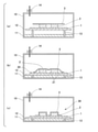
減圧チャンバー内で光半導体素子を搭載する光半導体素子搭載基板上に封止フィルムを載置し、前記減圧チャンバー内を減圧する工程、
前記封止フィルムを加熱して、前記封止フィルムの少なくとも周辺部を前記光半導体素子搭載基板の表面に熱融着させる工程、
前記減圧チャンバー内の減圧を解除して、前記封止フィルムで前記光半導体素子搭載基板を封止する工程を含み、
前記減圧チャンバー内の減圧を解除する時点の前記光半導体素子搭載基板の温度T2が、前記封止フィルムが0.02〜0.15MPaの引張強度及び150〜450%の破断伸度を示す温度であることを特徴にする。
本発明に係る封止光半導体デバイスの製造方法は、
(1) 減圧チャンバー内で光半導体素子を搭載する光半導体素子搭載基板上に封止フィルムを載置して、前記減圧チャンバー内を減圧する工程、
(2) 前記封止フィルムを加熱して、前記封止フィルムの少なくとも周辺部を前記光半導体素子搭載基板の表面に熱融着させる工程、及び、
(3) 前記減圧チャンバー内の減圧を解除して、前記封止フィルムで前記光半導体素子搭載基板を封止する工程を含み、
前記減圧チャンバー内の減圧を解除する時点の前記光半導体素子搭載基板の温度T2が、前記封止フィルムが0.02〜0.15MPaの引張強度及び150〜450%の破断伸度を示す温度であることに特徴がある。
熱硬化性シリコーン組成物(東レ・ダウコーニング株式会社製、商品名LF−1200)に対して、75質量%、及び85質量%の量でYAG系黄色発光蛍光体粒子(Intematix社製、商品名NYAG4454−S、平均粒径8μm)を混合し、厚さ100μmの封止フィルムA(蛍光体粒子75質量%含有)、及び封止フィルムB(蛍光体粒子85質量%含有)を調製した。
光半導体素子搭載基板として、ガラス基板上に、奥行き1mm、幅1mm、高さ0.15mmの直方体状の光半導体素子を、縦に10個、横に10個配置した光半導体素子搭載基板を用いた。光半導体素子間の距離Lは均等に0.15mmであり、光半導体素子の高さTと光半導体素子間の距離Lとのアスペクト比(T/L)は1であった。
封止フィルムA〜Dを用いて、上記半導体素子搭載基板に対して真空ラミネーションを行った。減圧チャンバーとしては、真空ポンプと接続したリフトピン昇降機構を有する真空ラミネータ(日清紡メカトロニクス社製、商品名PVL−0505Sリフトピン機構付き)を用いた。まず、真空ラミネータ内の熱板から離れた位置に配置されたリフトピン昇降機構により昇降可能な中板上に光半導体素子搭載基板を設置し、その上に封止フィルムA、B、C、又はDを載置した。次いで、真空ポンプを駆動させて真空ラミネータ内を133Paまで減圧させた。次いで、中板を下降させて100℃〜180℃に加熱された熱板に接触させた。その後、封止フィルムを3分〜7分間かけて加熱し、光半導体素子搭載基板の温度が所定の温度T2に達した時点で10秒間かけて減圧を大気圧まで戻して、封止光半導体デバイスを得た。

2 光半導体素子
3 封止フィルム
10 真空ラミネータ
11 熱板
12 中板
13 リフトピン
14〜16 開口
20 封止フィルムの周辺部
21 気密空間
30 封止光半導体デバイス
40 ダイアフラム型真空ラミネータ
41 ダイアフラムゴム膜
42 上室
43 下室
50 ラミネーション治具
51 スプリング
52 上枠
Claims (7)
- 減圧チャンバー内で光半導体素子を搭載する光半導体素子搭載基板上に封止フィルムを載置し、前記減圧チャンバー内を減圧する工程、
前記封止フィルムを加熱して、前記封止フィルムの少なくとも周辺部を前記素子搭載基板の表面に熱融着させる工程、及び
前記減圧チャンバー内の減圧を解除して、前記封止フィルムで前記光半導体素子搭載基板を封止する工程を含む、封止光半導体デバイスの製造方法であって、
前記減圧チャンバー内の減圧を解除する時点の前記光半導体素子搭載基板の温度T2は、前記封止フィルムが0.02〜0.15MPaの引張強度及び150〜450%の破断伸度を示す温度である、封止光半導体デバイスの製造方法。 - 前記封止フィルムが、熱硬化性シリコーン樹脂で構成される、請求項1に記載の封止光半導体デバイスの製造方法。
- 前記封止フィルムが、90質量%以下の蛍光体を含む、請求項1又は2に記載の封止光半導体デバイスの製造方法。
- 前記封止フィルムが、10μm以上300μm以下の厚さを有する、請求項1〜3のいずれか一項に記載の封止光半導体デバイスの製造方法。
- 前記温度T2が、70℃以上180℃以下である、請求項1〜3のいずれか一項に記載の封止光半導体デバイスの製造方法。
- 前記光半導体素子搭載基板において、光半導体素子が複数搭載され、前記光半導体素子間の最小距離が、前記封止フィルムの厚さよりも長い、請求項1〜5のいずれか一項に記載の封止光半導体デバイスの製造方法。
- 前記光半導体素子搭載基板において、光半導体素子が複数搭載され、前記光半導体素子の高さTと、隣り合う2つの光半導体素子間の距離Lとのアスペクト比(T/L)が、最大で3以下である、請求項1〜6のいずれか一項に記載の封止光半導体デバイスの製造方法。
Applications Claiming Priority (3)
| Application Number | Priority Date | Filing Date | Title |
|---|---|---|---|
| JP2017172928 | 2017-09-08 | ||
| JP2017172928 | 2017-09-08 | ||
| PCT/JP2018/032432 WO2019049794A1 (ja) | 2017-09-08 | 2018-08-31 | 封止光半導体デバイスの製造方法 |
Publications (2)
| Publication Number | Publication Date |
|---|---|
| JPWO2019049794A1 JPWO2019049794A1 (ja) | 2020-07-27 |
| JP6987871B2 true JP6987871B2 (ja) | 2022-01-05 |
Family
ID=65634136
Family Applications (1)
| Application Number | Title | Priority Date | Filing Date |
|---|---|---|---|
| JP2019540934A Active JP6987871B2 (ja) | 2017-09-08 | 2018-08-31 | 封止光半導体デバイスの製造方法 |
Country Status (7)
| Country | Link |
|---|---|
| US (1) | US11139419B2 (ja) |
| EP (1) | EP3680944B1 (ja) |
| JP (1) | JP6987871B2 (ja) |
| KR (1) | KR102330418B1 (ja) |
| CN (1) | CN111033770B (ja) |
| TW (1) | TWI787326B (ja) |
| WO (1) | WO2019049794A1 (ja) |
Families Citing this family (1)
| Publication number | Priority date | Publication date | Assignee | Title |
|---|---|---|---|---|
| CN115052742A (zh) * | 2019-12-27 | 2022-09-13 | 陶氏东丽株式会社 | 层叠体以及由该层叠体构成的电子零件 |
Family Cites Families (22)
| Publication number | Priority date | Publication date | Assignee | Title |
|---|---|---|---|---|
| JPH05110256A (ja) | 1991-10-21 | 1993-04-30 | Hitachi Chem Co Ltd | 多層プリント板用銅張り積層板の製造方法 |
| JPH06190956A (ja) | 1992-12-25 | 1994-07-12 | Yokohama Rubber Co Ltd:The | ハニカムサンドイッチパネルの製造方法 |
| JP3375217B2 (ja) * | 1994-10-14 | 2003-02-10 | 新日本石油化学株式会社 | 電気電子部品用封止材 |
| JPH08264577A (ja) * | 1995-03-24 | 1996-10-11 | Nitto Denko Corp | 半導体パッケージの製造方法およびこれに用いられる金型 |
| KR101173713B1 (ko) | 2004-04-28 | 2012-08-13 | 니폰 제온 가부시키가이샤 | 적층체, 발광 소자 및 그의 사용 |
| JP4872587B2 (ja) * | 2006-10-12 | 2012-02-08 | 日立化成工業株式会社 | 封止フィルム、及びこれを用いた半導体装置 |
| TW201216526A (en) | 2010-08-20 | 2012-04-16 | Koninkl Philips Electronics Nv | Lamination process for LEDs |
| US8597988B2 (en) | 2010-11-18 | 2013-12-03 | Bridgelux, Inc. | System for flash-free overmolding of led array substrates |
| KR102228997B1 (ko) * | 2012-03-29 | 2021-03-18 | 루미리즈 홀딩 비.브이. | Led 응용들을 위한 무기 바인더 내의 형광체 |
| CN104170101B (zh) | 2012-04-12 | 2018-02-09 | 美国圣戈班性能塑料公司 | 制造发光装置的方法 |
| JP6321910B2 (ja) * | 2013-03-26 | 2018-05-09 | 日東電工株式会社 | 封止シート、半導体装置の製造方法及び封止シート付き基板 |
| KR102092707B1 (ko) | 2013-09-17 | 2020-03-25 | 삼성디스플레이 주식회사 | 플렉서블 디스플레이 장치와, 이의 제조 방법 |
| CN105637660B (zh) | 2013-11-07 | 2018-11-09 | 东丽株式会社 | 层叠体及使用所述层叠体的发光装置的制造方法 |
| US9853193B2 (en) * | 2014-06-04 | 2017-12-26 | Dow Corning Corporation | Imprinting process of hot-melt type curable silicone composition for optical devices |
| CN104212049B (zh) * | 2014-08-26 | 2016-06-01 | 大连欧思特科技有限公司 | 一种热缩管和制备方法以及在led灯丝封装上的应用 |
| JP6245136B2 (ja) * | 2014-10-20 | 2017-12-13 | 信越化学工業株式会社 | 光半導体素子封止用シリコーン樹脂組成物及び光半導体装置 |
| KR102468894B1 (ko) | 2014-10-24 | 2022-11-22 | 다우 실리콘즈 코포레이션 | 순응성으로 코팅된 물품을 형성하기 위한 진공 라미네이션 방법 및 이로부터 형성된 연관된 순응성으로 코팅된 물품 |
| JP2016171314A (ja) | 2015-03-09 | 2016-09-23 | 日東電工株式会社 | 封止シート、封止光半導体素子の製造方法および光半導体装置の製造方法 |
| JP2016171315A (ja) | 2015-03-09 | 2016-09-23 | 日東電工株式会社 | 貼着シート、貼着光半導体素子の製造方法および光半導体装置の製造方法 |
| US10014108B2 (en) | 2015-03-13 | 2018-07-03 | Avx Corporation | Low profile multi-anode assembly |
| CN107995920B (zh) | 2015-09-29 | 2021-03-12 | 东丽株式会社 | 荧光体组合物、荧光体片材及使用它们的形成物、 led芯片、led封装体、发光装置、背光单元 |
| JP6677550B2 (ja) | 2016-03-25 | 2020-04-08 | 東芝キヤリア株式会社 | 冷凍サイクル装置の室外機の保護部材 |
-
2018
- 2018-08-16 TW TW107128570A patent/TWI787326B/zh active
- 2018-08-31 CN CN201880050214.6A patent/CN111033770B/zh active Active
- 2018-08-31 JP JP2019540934A patent/JP6987871B2/ja active Active
- 2018-08-31 EP EP18854322.7A patent/EP3680944B1/en active Active
- 2018-08-31 KR KR1020207003021A patent/KR102330418B1/ko active IP Right Grant
- 2018-08-31 US US16/634,808 patent/US11139419B2/en active Active
- 2018-08-31 WO PCT/JP2018/032432 patent/WO2019049794A1/ja unknown
Also Published As
| Publication number | Publication date |
|---|---|
| CN111033770A (zh) | 2020-04-17 |
| TW201913830A (zh) | 2019-04-01 |
| WO2019049794A1 (ja) | 2019-03-14 |
| EP3680944B1 (en) | 2022-06-15 |
| TWI787326B (zh) | 2022-12-21 |
| US20200373457A1 (en) | 2020-11-26 |
| US11139419B2 (en) | 2021-10-05 |
| KR102330418B1 (ko) | 2021-12-01 |
| KR20200026268A (ko) | 2020-03-10 |
| JPWO2019049794A1 (ja) | 2020-07-27 |
| CN111033770B (zh) | 2023-03-14 |
| EP3680944A4 (en) | 2021-06-02 |
| EP3680944A1 (en) | 2020-07-15 |
Similar Documents
| Publication | Publication Date | Title |
|---|---|---|
| JP6957630B2 (ja) | 封止光半導体デバイスの製造方法 | |
| JP5680210B2 (ja) | 封止層被覆半導体素子および半導体装置の製造方法 | |
| EP2712908A2 (en) | Phosphor adhesive sheet, optical semiconductor element-phosphor layer pressure-sensitive adhesive body, and optical semiconductor device | |
| JP2014096491A (ja) | 蛍光体層被覆半導体素子、その製造方法、半導体装置およびその製造方法 | |
| US9048401B2 (en) | Producing method of semiconductor device | |
| WO2017221606A1 (ja) | 蛍光体層付光半導体素子およびその製造方法 | |
| JP6987871B2 (ja) | 封止光半導体デバイスの製造方法 | |
| WO2015029664A1 (ja) | 封止半導体素子および半導体装置の製造方法 | |
| JP2013206925A (ja) | 半導体基板、半導体装置、および、半導体装置の製造方法 |
Legal Events
| Date | Code | Title | Description |
|---|---|---|---|
| A621 | Written request for application examination |
Free format text: JAPANESE INTERMEDIATE CODE: A621 Effective date: 20200128 |
|
| RD03 | Notification of appointment of power of attorney |
Free format text: JAPANESE INTERMEDIATE CODE: A7423 Effective date: 20200306 |
|
| RD04 | Notification of resignation of power of attorney |
Free format text: JAPANESE INTERMEDIATE CODE: A7424 Effective date: 20200512 |
|
| A131 | Notification of reasons for refusal |
Free format text: JAPANESE INTERMEDIATE CODE: A131 Effective date: 20210301 |
|
| A521 | Request for written amendment filed |
Free format text: JAPANESE INTERMEDIATE CODE: A523 Effective date: 20210601 |
|
| A131 | Notification of reasons for refusal |
Free format text: JAPANESE INTERMEDIATE CODE: A131 Effective date: 20210712 |
|
| A521 | Request for written amendment filed |
Free format text: JAPANESE INTERMEDIATE CODE: A523 Effective date: 20210818 |
|
| TRDD | Decision of grant or rejection written | ||
| A01 | Written decision to grant a patent or to grant a registration (utility model) |
Free format text: JAPANESE INTERMEDIATE CODE: A01 Effective date: 20211108 |
|
| A61 | First payment of annual fees (during grant procedure) |
Free format text: JAPANESE INTERMEDIATE CODE: A61 Effective date: 20211201 |
|
| R150 | Certificate of patent or registration of utility model |
Ref document number: 6987871 Country of ref document: JP Free format text: JAPANESE INTERMEDIATE CODE: R150 |